subject:-digital electronics code –bca-106 unit-i
TRANSCRIPT

SUBJECT:-Digital electronics
CODE –BCA-106
UNIT-I
Logic gates NOT , AND, OR, Universal gates- NAND , NOR. EX-OR and EX-NOR gates.
Diode and Transistor as a switch
Logic Families-RTL,DTL,TTL,ECL,CMOS – (Main features only - without details of circuit
connections and working). Definition of- current and voltage parameters, noise margin, Fan-in,
Fan-out
Boolean Algebra
Basics Laws of Boolean Algebra, Logic Gates, Simplifications of Boolean equations using
K-maps .
UNIT-II
Review of various number systems (Binary, Octal, Hexadecimal), Definition of BCD , Gray
codes and Excess – 3 codes and their application (without design of code convertors)
Parity generation and Checking.
Arithmetic Circuits
Adder, Subtractor, Parallel binary adder/Subtractor, binary multiplier and divider.
Combinational Circuits
Multiplexers, De-Multiplexers, decoders, encoders,.
UNIT-III
Flip-flops
S-R, D, J-K, T, Clocked Flip-flop, Race around condition, Master slave Flip-Flop,
Realisation of one flip-flop using other flip-flop.
Shift Registers
Serial-in-serial-out, serial-in-parallel-out, parallel-in-serial-out and parallel-in-parallel-out,
Bi-directional shift register.
UNIT-IV
Counters
Ripple counter, Synchronous Counter, Modulo Counters, Ring Counter, Twisted Ring Counter.
Memory Devices - RAM, ROM, PAL & PLA .

UNIT -1
Logic Gates
Gates
Logic gates (or simply gates) are the fundamental building blocks of digital circuitry. As
their name implies, they function by “opening” or “closing” to admit or reject the flow of
digital information. Gates implement electronically simple logical operations on boolean
(Bool’s algebra) variables, i.e. variables that can have only one of two states (0/1,
low/high, false/true). In the following figure the accepted electronic symbols for different
gates are shown, along with their corresponding “truth tables” and their symbolic logical
expressions. All variables (X, A, B, …) are booleans.
The basic logic gates are AND, NOT, OR, NAND, NOR, XOR.
The most typical logical operations are implemented by AND and OR gates. The logical expres-
sion for the AND operation is “if A is true AND B is true then X is true”, and for the OR
operation is “if A is true OR B is true then X is true”. The inverted logic AND and OR gates are
commonly known as NAND (Not AND) and NOR (Not OR) gates. A XOR (Exclusive-OR) gate
implements the logical expression “if A is different than B then X is true”, hence sometimes this
gate is called “inequality comparator”.

The buffer and the inverter are not gates but their use is closely associated with them. A
buffer doesn’t change the logic state of its input. It is only occasionally used for increasing the
fan-out, i.e. the capability of the output of one gate to drive a number of other gates. The inverter
is much more important and it is used for inverting a logic state, i.e. for performing the logical
operation of negation (NOT). The logical expressions for a buffer and an inverter are “X is A”
and “X is NOT A”, respectively. AND, OR, NAND and NOR gates can have more than 2 inputs.
The Exclusive-NOR Gate function or Ex-NOR for short, is a digital logic gate that is the reverse
or complementary form of the Exclusive-OR function. The Exclusive-NOR gate is a
combination of the Exclusive-OR gate and the NOT gate but has a truth table similar to the
standard NOR gate in that it has an output that is normally at logic level "1" and goes "LOW" to
logic level "0" when ANY of its inputs are at logic level "1".
Ex-NOR Gate Equivalent
Diode and Transistor as a switch
The transistor is an amplifier, but can be used as a switch by using the transistor in its saturated
region. This can be used to switch a significantly larger current than the input signal. As a switch
the transistor is often used to take a signal from a digital circuit and use it to switch larger loads
than the integrated circuit (IC) can provide.
The circuit below shows a common simple configuration for a transistor switch circuit. It
comprises of one NPN transistor, and depicts two Resistors. The Resistor RL is not normally a
resistor, but represents the resistive value of a device that is being switched. This could be a lamp
or relay or some other device that needs a larger current than the input is able to drive directly.
The resistor at the base Rb is a resistor used to prevent damage at the base of the transistor. This
needs to be large enough to prevent damage to the transistor, but should still allow sufficient
current to ensure the transistor switches on. Details of how to determine the size of the resistor
are explained below.

How the circuit works
For a transistor to act as a switch it needs to be activated as the saturation region. When switched
on in saturation the transistor acts almost as a short circuit allowing current through the load.
If the load being switched is an inductive device, such as a motor, solenoid or relay then a diode
should be connected in the reverse direction across the load to prevent any back EMF from
damaging the transistor.
Logic Families
IC Logic Families:-
Thus far, we have specified the logic level as either 0 or 1, or HIGH or LOW. In circuit
implementation, we will have to specify the actual voltage/current levels that constitute a HIGH
or a LOW. These standardized voltage/current levels are grouped in families of digital ICs so
that ICs belonging to the same family will have the same characteristics.
� The feature to be concerned of IC logic families:
– fan-out
• The no. of standard loads can be connected to the output of the gate
without degrading its normal operation
• Sometimes the term loading is used for Fan out
– Power dissipation
• The power needed by the gate
• Expressed in mW
– Propagation delay
• The average transition-delay time for the signal to propagate from input to
output when the binary signal changes in value
– Noise margin
• The unwanted signals are referred to as noise

• Noise margin is the maximum noise added to an input signal of a digital
circuit that does not cause an undesirable change in the circuit output .
• A fan-in of a logic gate is the number of bits that are input to the gate
� Fan out:-
Fan-out is a term that defines the maximum number of digital inputs that the output of a
single logic gate can feed. Most transistor-transistor logic ( TTL ) gates can feed up to 10
other digital gates or devices. Thus, a typical TTL gate has a fan-out of 10.
Characteristics of Ecl
� Nonsaturated digital logic family
� Propagation rate as low as 1-2ns
� Used mostly in high speed circuits
� Noise immunity and power dissipation is the worst of all logic families.
� High level -0.8V, Low level -1.8V
� Including
– Differential input amplifier
– Internal temperature and voltage compensated bias network
– Emitter-follower outputs
Characteristics of CMOS logic:
1. Dissipates low power: The power dissipation is dependent on the power supply voltage,
frequency, output load, and input rise time. At 1 MHz and 50 pF load, the power dissipation is
typically 10 nW per gate.
2. Short propagation delays: Depending on the power supply, the propagation delays are
usually around 25 nS to 50 nS.
3. Rise and fall times are controlled: The rise and falls are usually ramps instead of step
functions, and they are 20 - 40% longer than the propagation delays.
4. Noise immunity approaches 50% or 45% of the full logic swing.
5. Levels of the logic signal will be essentially equal to the power supplied since the input
impedance is so high.
Characteristics of TTL logic: 1. Power dissipation is usually 10 mW per gate.
2. Propagation delays are 10 nS when driving a 15 pF/400 ohm load.
3. Voltage levels range from 0 to Vcc where Vcc is typically 4.75V - 5.25V. Voltage range
0V - 0.8V creates logic level 0. Voltage range 2V - Vcc creates logic level 1.

CMOS compared to TTL: 1. CMOS components are typically more expensive that TTL equivalents.
2. CMOS circuits do not draw as much power as TTL circuits while at rest. However,
CMOS power consumption increases faster with higher clock speeds than TTL does.
Lower current draw requires less power supply distribution, therefore causing a simpler
and cheaper design.
3. Due to longer rise and fall times, the transmission of digital signals become simpler and
less expensive with CMOS chips.
4. CMOS components are more susceptible to damage from electrostatic discharge than
TTL components.
Resistor-Transistor Logic (RTL) Resistor-Transistor Logic (RTL) was invented around 1956. This type of technology, unlike DL,
uses active devices such as transistors and therefore can provide inversion. The voltage range
goes from 0V for low (0) to 3.5V for high (1). RTL is very inefficient because it dissipates a
great amount of power through heat.
RTL has two variants that attempt to improve some of its aspects:
1. When inputs are directly connected to the gate of the BJT, in order to save space and reduce
fabrication costs, RTL is known as Direct-Coupled Transistor Logic (DCTL).
2. When capacitors are placed in parallel with input resistors, to speed up operation, RTL is
known as Resistor-Capacitor Transistor Logic (RCTL).
Fairchild Semiconductor introduced the first generation of RTL monolithic integrated circuits in
either 1962 or 1963. RTL is an obsolete digital logic family.
Diode-Transistor Logic (DTL):-
Diode-Transistor Logic (DTL) was invented in the 1950s. It is a major improvement over DL
and RTL because it eliminates signal degradation and reduces power dissipation by means of a
transistor which restores digital values and a set of input diodes which replace input resistors.
DTL has two variants that attempt to improve some of its aspects:
1. When a capacitor is placed in parallel with the base resistor and an inductor is placed in series
with the collector resistor, DTL is known as Complemented Transistor Diode Logic (CTDL).

2. When a Zener diode and a single power supply are connected to the base of the transistor,
DTL is known as High-Threshold Logic (HTL).
Signetics introduced the first generation of DTL monolithic integrated circuits in 1962.
DTL was used in the IBM 1401 decimal computer that was delivered in 1959.
Boolean Algebra
The following are a set of basic identities forming a subset of the laws of logic.
Rules of Boolean Algebra
1. A is either 0 or 1
2. Commutative
1. A.B = B.A
2. A+B = B+A
3. Distributive
1. A.(B+C) = A.B + A.C
2. A + B.C = (A+B).(A+C)
4. Identity
1. A + 0 = A
2. A + 1 = 1
3. A.1 = A
4. A.0 = 0
5. Inverse
1. A + not(A) = 1
2. A.not(A) = 0
6. De Morgan's Laws
1. not(A+B) = not(A).not(B)
2. not(A.B) = not(A) + not(B)
Karnaugh Maps
1. A Karnaugh Map (sometimes called K-map) for a Boolean function f(x1,x2,...,xn) is a
rectangular grid of size 2k × 2n-k constructed as follows.
2. k is equal to n/2
3. Rows represent truth assignments for k variables x1,x2,...,xk and are labeled with
conjunction of literals corresponding to the truth assignments for the rows.
4. The Hamming distance between the truth assignments of consecutive rows is always
equal to 1.
5. Columns represent truth assignments for (n-k) variables xk+1,xk+2,...,xn and are labeled
with conjunction of literals corresponding to the truth assignments for the columns.

6. The Hamming distance between the truth assignments of consecutive columns is always
equal to 1.
7. Each cell on a column and a row is 1 if the Boolean function f(x1,x2,...,xn) is equal to 1
for the truth assignment represented by the column and the row. The cell has a symbol
"X" (called "don't care") if a value of the Boolean function doesn't matter. Otherwise, the
cell is empty.
Minimal Sum
A sum of products (SOP) expression such that no SOP expression for Y has fewer
product terms and any SOP expression with the same number of product terms has at
least as many literals.
UNIT -II
NUMBER SYSTEM
A number system of base (also called radix) r is a system, which has r distinct symbols for r
digits. A number is represented by a string of these symbolic digits. To determine the quantity
that the number represents, we multiply the number by an integer power of r depending on the
place it is located and then find the sum of weighted digits.
Binary-coded decimal (BCD) is a digital encoding method for numbers using decimal
notation, with each decimal digit represented by its own binary sequence. In BCD, a numeral is
usually represented by four bits which, in general, represent the decimal range 0 through 9.
Examples:
Convert decimal 4019 to BCD
4 0 1 9
0100 0000 0001 1001
The BCD equivalent of (4019)10 is 0100 0000 0001 1001
Convert BCD number 0001 1001 0000 0111 to decimal
0001 1001 0000 0111

1 9 0 7
The decimal equivalent of BCD Number 0001 1001 0000 0111 is (1907)10. BCD numbers are
useful wherever decimal information is transferred into a computer. The pocket calculator is
one of the best examples for the application of BCD numbers. Other examples of BCD system
are electronic counters, digital voltmeter and digital clocks.
Octal to Binary
Converting from octal to binary is as easy as converting from binary to octal. Simply look up
each octal digit to obtain the equivalent group of three binary digits.
Octal: 0 1 2 3 4 5 6 7
Binary: 000 001 010 011 100 101 110 111
Octal = 3 4 5
Binary = 011 100 101 = 011100101 binary
Octal to Hexadecimal
When converting from octal to hexadecimal, it is often easier to first convert the octal number
into binary and then from binary into hexadecimal. For example, to convert 345 octal into hex:
(from the previous example)
Octal = 3 4 5
Binary = 011 100 101 = 011100101 binary
Drop any leading zeros or pad with leading zeros to get groups of four binary digits (bits):
Binary 011100101 = 1110 0101
Octal to Decimal
Converting octal to decimal can be done with repeated division.

1. Start the decimal result at 0.
2. Remove the most significant octal digit (leftmost) and add it to the result.
3. If all octal digits have been removed, you’re done. Stop.
4. Otherwise, multiply the result by 8.
5. Go to step 2.
Octal Digits Operation Decimal Result Operation Decimal Result
345 +3 3 × 8 24
45 +4 28 × 8 224
5 +5 229 done.
The conversion can also be performed in the conventional mathematical way, by showing each
digit place as an increasing power of 8.
345 octal = (3 * 82) + (4 * 8
1) + (5 * 8
0) = (3 * 64) + (4 * 8) + (5 * 1) = 229 decimal
Hexadecimal to Binary
Converting from hexadecimal to binary is as easy as converting from binary to hexadecimal.
Simply look up each hexadecimal digit to obtain the equivalent group of four binary digits.
Hexadecimal: 0 1 2 3 4 5 6 7
Binary: 0000 0001 0010 0011 0100 0101 0110 0111
Hexadecimal: 8 9 A B C D E F
Binary: 1000 1001 1010 1011 1100 1101 1110 1111
Hexadecimal = A 2 D E
Binary = 1010 0010 1101 1110 = 1010001011011110 binary

Hexadecimal to Octal
When converting from hexadecimal to octal, it is often easier to first convert the hexadecimal
number into binary and then from binary into octal. For example, to convert A2DE hex into
octal:
(from the previous example)
Hexadecimal = A 2 D E
Binary = 1010 0010 1101 1110 = 1010001011011110 binary
Add leading zeros or remove leading zeros to group into sets of three binary digits.
Binary: 1010001011011110 = 001 010 001 011 011 110
Then, look up each group in a table:
Binary: 000 001 010 011 100 101 110 111
Octal: 0 1 2 3 4 5 6 7
Binary = 001 010 001 011 011 110
Octal = 1 2 1 3 3 6 = 121336 octal
Therefore, through a two-step conversion process, hexadecimal A2DE equals binary
1010001011011110 equals octal 121336.
Hexadecimal to Decimal
Converting hexadecimal to decimal can be performed in the conventional mathematical way, by
showing each digit place as an increasing power of 16. Of course, hexadecimal letter values need
to be converted to decimal values before performing the math.
Hexadecimal: 0 1 2 3 4 5 6 7
Decimal: 0 1 2 3 4 5 6 7

Hexadecimal: 8 9 A B C D E F
Decimal: 8 9 10 11 12 13 14 15
A2DE hexadecimal:
= ((A) * 163) + (2 * 16
2) + ((D) * 16
1) + ((E) * 16
0)
= (10 * 163) + (2 * 16
2) + (13 * 16
1) + (14 * 16
0)
= (10 * 4096) + (2 * 256) + (13 * 16) + (14 * 1)
= 40960 + 512 + 208 + 14
= 41694 decimal
EXCESS – 3 CODE:
The Excess-3 code is a decimal code that has been used in older computers. This is an un-
weighted code. Its binary code assignment is obtained from the corresponding BCD
equivalentbinary number after the addition of binary 3 (0011).
DECIMAL BCD
0 0000
1 0001
2 0010
3 0011
4 0100
5 0101
6 0110
7 0111
8 1000
9 1001
10 0001 0000

EXCESS 3 CODE
0011
0100
0101
0110
0111
1000
1001
1010
1011
1100
0100 0011
GRAY CODE
This is a variable weighted code and is cyclic. This means that it is arranged so that every
transition from one value to the next value involves only one bit change. The gray code is
sometimes referred to as reflected binary, because the first eight values compare with those of
the last 8 values, but in reverse order.
Decimal Binary Gray
0 0000 0000
1 0001 0001
2 0010 0011
3 0011 0010
4 0100 0110
5 0101 0111
6 0110 0101
7 0111 0100
8 1000 1100

The gray code is often used in mechanical applications such as shaft
encoders. Arithmetic
This is binary addition with the carry ignored.
Converting Gray Code to Binary A. write down the number in gray code
B. the most significant bit of the binary number is the most significant
bit of the gray code
C. add (using modulo 2) the next significant bit of the binary number to
the next significant bit of the gray coded number to obtain the next
binary bit
D. repeat step C till all bits of the gray coded number have been added modulo 2
the resultant number is the binary equivalent of the gray number
Parity generation and Checking.:-
A parity generator checks the data to be transmitted and outputs a 0(parity bit) if the number of
logic 1's in the data is even, and a logic 0 if the number is odd. So a checker takes the transmitted
data and the parity bit and will compare the two, and if they are both of the same logic then the
you can conclude that the data was received successfully (i.e no bits were lost during
transmission). Parity checker/generator use the exact same devices, but with one comparing
instead of generating.
Half-Adder It computes the sum of two single bits x and y by producing the sum bit s and the carry bit c.
x ---------------------------------------
+ y x y | u v
---- ---------------------------------------
cs 0 0 | 0 0
0 1 | 0 1
1 0 | 0 1
1 1 | 1 0
---------------------------------------
Design
------
c = x y
_ _
s = x y + x y
9 1001 1101
10 1010 1111
11 1011 1110
12 1100 1010
13 1101 1011
14 1110 1001
15 1111 1000

Full-Adder It computes the sum of two single bits x and y and a carry cin from the lower-order bit, by
producing the sum bit s and the carry bit cout to the higher-order bit.
----------------------------------------------
x y c | c s
in out
----------------------------------------------
0 0 0 | 0 0
0 0 1 | 0 1
0 1 0 | 0 1
0 1 1 | 1 0
1 0 0 | 0 1
1 0 1 | 1 0
1 1 0 | 1 0
1 1 1 | 1 1
----------------------------------------------

Subtractor : Subtractor is the one which used to subtract two binary number and provides
Difference and Borrow as a output.basically we have two types of subtractor.
Half Subtractor
Full Subtractor
Half Subtractor :Half Subtractor is used for subtracting one single bit binary number from
another single bit binary number.The truth table of Half Subtractor is shown below.
Difference = A'B+AB'=A B

Borrow=A'B
The logic Diagram of Half Subtractor is shown below.
Full Subtractor : A logic Circuit Which is used for Subtracting Three Single bit Binary numbers
is known as Full Subtractor.The Truth Table of Full Subtractor is Shown Below.
From the Truth Table The Difference and Borrow will written as
Difference=A'B'C+A'BB'+AB'C'+ABC
Reduce it like adder
Then We got
Difference=A B C
Borrow=A'B'C+A'BC'+A'BC+ABC
=A'B'C+A'BC'+A'BC+A'BC+A'BC+ABC ----------> A'BC=A'BC+A'BC+A'BC

=A'C(B'+B)+A'B(C'+C)+BC(A'+A)
Borrow=A'C+A'B+BC
The logic diagram of Full Subtractor is Shown below
Parallel Binary Adder/subtractor
The use of one half-adder or one full-adder alone are great for adding up two binary numbers
with a length of one bit each, but what happens when the computer needs to add up two binary
numbers with a longer length. The fastest way by far is to use the Parallel Binary Adder. The
parallel binary adder uses one half-adder, along with one or more full adders. The number of
total adders needed depends on the length of the largest of the two binary numbers that are to be
added. For example, if we were to add up the binary numbers 1011 and 1, we would need four
adders in total, because the length of the larger number is four. here is a demonstration of how a
four-bit parallel binary adder works, using 1101 and 1011 as the two numbers to add. The
parallel binary subtractor is same as parallel binary adder only the difference is this that in
subtractor we use borrow inspite of giving carry to another bit.

Just like when we add without the computer, in the parallel binary adder, the computer adds from
right to left. Here is a step by step list, showing that what happens in the parallel Binary Adder
1 In the only half-adder, inputs of 1 and 1 give us 0 with a carry of 1.
2 In the first full-adder (going from right to left), the inputs of 1 and 0 plus the carry of 1 from
the half-adder give us a 0 with a carry of 1.
3 In the second full adder, the inputs of 0 and 1 plus the carry of 1 from the previous full-adder
give us a 0 with a carry of 1.
4 In the third and final full adder, the inputs of 1 and 1 plus the carry of 1 from the previous
full-adder give us a 1 with a carry of 1.

5 Since there are no more numbers to add up, and there is still a carry of 1, the carry becomes
the most significant bit.
6 The sum of 1101 and 1011 is 11000.
Parallel Binary Multiplier/ divider:
A binary multiplier is an electronic circuit used in digital electronics, such as a computer, to
multiply two binary numbers. It is built using binary adders. A binary computer does exactly the
same, but with binary numbers. In binary encoding each long number is multiplied by one digit
(either 0 or 1), and that is much easier than in decimal, as the product by 0 or 1 is just 0 or the
same number. Therefore, the multiplication of two binary numbers comes down to calculating
partial products (which are 0 or the first number), shifting them left, and then adding them
together.
A variety of computer arithmetic techniques can be used to implement a digital multiplier. Most
techniques involve computing a set of partial products, and then summing the partial products
together. This process is similar to the method taught to primary schoolchildren for conducting
long multiplication on base-10 integers, but has been modified here for application to a base-2
(binary) numeral system. This is much simpler than in the decimal system, as there is no table of
multiplication to remember: just shifts and adds. This method is mathematically correct and has
the advantage that a small CPU may perform the multiplication by using the shift and add
features of its arithmetic logic unit rather than a specialized circuit. The method is slow,
however, as it involves many intermediate additions. These additions take a lot of time. Faster
multipliers may be engineered in order to do fewer additions; a modern processor can multiply
two 64-bit numbers with 6 additions (rather than 64), and can do several steps in parallel.
The process is same as for Parallel Divider also.

Encoder :-
Encoder is a circuit which converts the analog signal in to the digital signal. An encoder is a
device, circuit, transducer, software program, algorithm or person that converts information from
one format or code to another, for the purposes of standardization, speed, secrecy, security, or
saving space by shrinking size.
Encoder Circuit Diagram
Decoder:-
A decoder is a device which does the reverse operation of an encoder, undoing the encoding so
that the original information can be retrieved. The same method used to encode is usually just
reversed in order to decode. It is a combinational circuit that converts binary information from n
input lines to a maximum of 2n unique output lines. Decoding is necessary in applications such
as data multiplexing, 7 segment display and memory address decoding.

The example decoder circuit would be an AND gate because the output of an AND gate is
"High" (1) only when all its inputs are "High." Such output is called as "active High output". If
instead of AND gate, the NAND gate is connected the output will be "Low" (0) only when all its
inputs are "High". Such output is called as "active low output".
Multiplexers:-
Multiplexer (or MUX) is a device that selects one of several analog or digital input signals and
forwards the selected input into a single line. A multiplexer of 2n inputs has n select lines, which
are used to select which input line to send to the output. Multiplexers are mainly used to increase
the amount of data that can be sent over the network within a certain amount of time and
bandwidth. A multiplexer is also called a data selector. An electronic multiplexer makes it
possible for several signals to share one device or resource, for example one A/D converter or
one communication line, instead of having one device per input signal. On the other hand, a
demultiplexer (or demux) is a device taking a single input signal and selecting one of many
data-output-lines, which is connected to the single input. A multiplexer is often used with a
complementary demultiplexer on the receiving end. An electronic multiplexer can be considered
as a multiple-input, single-output switch, and a demultiplexer as a single-input, multiple-output
switch.

De-Multiplexer:-
The demultiplexer is the inverse of the multiplexer, in that it takes a data input and n address
inputs. It has 2n outputs. The address input determine which data output is going to have the
same value as the data input. The other data outputs will have the value 0.
UNIT-III
Flip Flop:-
A flip-flop or latch is a circuit that has two stable states and can be used to store state
information. The circuit can be made to change state by signals applied to one or more control
inputs and will have one or two outputs. It is the basic storage element in sequential logic. Flip-
flops and latches are a fundamental building block of digital electronics systems used in
computers, communications, and many other types of systems.
Flip-flops and latches are used as data storage elements. Such data storage can be used for
storage of state, and such a circuit is described as sequential logic. When used in a finite-state
machine, the output and next state depend not only on its current input, but also on its current
state (and hence, previous inputs). It can also be used for counting of pulses, and for
synchronizing variably-timed input signals to some reference timing signal.
.
(a) Logic diagram
(b) Truth table
Basic flip-flop circuit with NOR gates

S.R Flip Flop:- When using static gates as building blocks, the most fundamental latch is the
simple SR latch, where S and R stand for set and reset. It can be constructed from a pair of cross-
coupled NOR logic gates. The stored bit is present on the output marked Q.
While the S and R inputs are both low, feedback maintains the Q and Q outputs in a constant
state, with Q the complement of Q. If S (Set) is pulsed high while R (Reset) is held low, then the
Q output is forced high, and stays high when S returns to low; similarly, if R is pulsed high while
S is held low, then the Q output is forced low, and stays low when R returns to low. The R = S =
1 combination is called a restricted combination or a forbidden state because, as both NOR gates
then output zeros, it breaks the logical equation Q = not Q. The combination is also inappropriate
in circuits where both inputs may go low simultaneously (i.e. a transition from restricted to
keep). The output would lock at either 1 or 0 depending on the propagation time relations
between the gates (a race condition). In certain implementations, it could also lead to longer
ringings (damped oscillations) before the output settles, and thereby result in undetermined
values (errors) in high-frequency digital circuits. Although this condition is usually avoided, it
can be useful in some applications.
To overcome the restricted combination, one can add gates to the inputs that would convert (S,R)
= (1,1) to one of the non-restricted combinations. That can be:
• Q = 1 (1,0) – referred to as an S-latch
• Q = 0 (0,1) – referred to as an R-latch
• Keep state (0,0) – referred to as an E-latch
Alternatively, the restricted combination can be made to toggle the output. The result is the JK
latch.
J-K FlipFlop:-
A JK flip-flop is a refinement of the SR flip-flop in that the indeterminate state of the SR type is
defined in the JK type. Inputs J and K behave like inputs S and R to set and clear the flip-flop
(note that in a JK flip-flop, the letter J is for set and the letter K is for clear). When logic 1 inputs
are applied to both J and K simultaneously, the flip-flop switches to its complement state, ie., if
Q=1, it switches to Q=0 and vice versa.

A clocked JK flip-flop is shown in Figure below. Output Q is AND with K and CP inputs so that
the flip-flop is cleared during a clock pulse only if Q was previously 1. Similarly, ouput Q' is
ANDed with J and CP inputs so that the flip-flop is set with a clock pulse only if Q' was
previously 1.
Note that because of the feedback connection in the JK flip-flop, a CP signal which remains a 1
(while J=K=1) after the outputs have been complemented once will cause repeated and
continuous transitions of the outputs. To avoid this, the clock pulses must have a time duration
less than the propagation delay through the flip-flop. The restriction on the pulse width can be
eliminated with a master-slave or edge-triggered construction. The same reasoning also applies
to the T flip-flop presented next.
(a) Logic diagram
(b) Graphical symbol
(c) Transition table

RACE AROUND CONDITION:-
Let us consider a JK Flip Flop (Hereby called FF). The excitation table of this FF is as follows :
J K Qn+1
0 0 Qn
0 1 0
1 0 1
1 1 Qn Bar
~ Complement of Qn
Let us say that a clock of certain frequency is fed to the FF, and consider the case of J=K=1, and
the propagation delay of FF is very very less than the clock pulse time
Then the FF continues complementing the output an unpredictable number of times, thus leading
to anomaly in the final output after the pulse time of the clock is completed
This condition is called Race Around condition and can be avoided by using a Master-Slave
JK FF
T Flip-Flop:-
The T flip-flop is a single input version of the JK flip-flop. As shown in Figure below, the T flip-
flop is obtained from the JK type if both inputs are tied together. The output of the T flip-flop
"toggles" with each clock pulse.
(a) Logic diagram

(b) Graphical symbol
Master-Slave Flip-Flop
A master-slave flip-flop is constructed from two separate flip-flops. One circuit serves as a
master and the other as a slave. The logic diagram of an SR flip-flop is shown in diagram. The
master flip-flop is enabled on the positive edge of the clock pulse CP and the slave flip-flop is
disabled by the inverter. The information at the external R and S inputs is transmitted to the
master flip-flop. When the pulse returns to 0, the master flip-flop is disabled and the slave flip-
flop is enabled. The slave flip-flop then goes to the same state as the master flip-flop.
Logic diagram of a master-slave flip-flop
The timing relationship is shown in diagram and is assumed that the flip-flop is in the clear state
prior to the occurrence of the clock pulse. The output state of the master-slave flip-flop occurs on
the negative transition of the clock pulse. Some master-slave flip-flops change output state on the
positive transition of the clock pulse by having an additional inverter between the CP terminal
and the input of the master.

Timing relationship in a master slave flip-flop
D Flip Flop:-
This latch exploits the fact that in the two active input combinations (01 and 10) of a gated SR
latch R is the complement of S. The input NAND stage converts the two D input states (0 and 1)
to these two input combinations for the next SR latch by inverting the data input signal. The low
state of the enable signal produces the inactive "11" combination. Thus a gated D-latch may be
considered as a one-input synchronous SR latch. This configuration prevents from applying the
restricted combination to the inputs. It is also known as transparent latch, data latch, or
simply gated latch. It has a data input and an enable signal (sometimes named clock, or control).
The word transparent comes from the fact that, when the enable input is on, the signal propagates
directly through the circuit, from the input D to the output Q.
Transparent latches are typically used as I/O ports or in asynchronous systems, or in synchronous
two-phase systems (synchronous systems that use a two-phase clock), where two latches
operating on different clock phases prevent data transparency as in a master–slave flip-flop..
The truth table shows that when
the enable/clock input is 0,
the D input has no effect on the output. When E/C(Enable clock) is high, the output equals D.
Clocked SR Flip-Flop
The clocked SR flip-flop shown in diagram consists of a basic NOR flip-flop and two AND
gates. The outputs of the two AND gates remain at 0 as long as the clock pulse (or CP) is 0,
regardless of the S and R input values. When the clock pulse goes to 1, information from the S
Gated D latch truth table
E/C D
Q Q Comment
0 X Qprev Qprev No change
1 0 0 1 Reset
1 1 1 0 Set

and R inputs passes through to the basic flip-flop. With both S=1 and R=1, the occurrence of a
clock pulse causes both outputs to momentarily go to 0. When the pulse is removed, the state of
the flip-flop is indeterminate, ie., either state may result, depending on whether the set or reset
input of the flip-flop remains a 1 longer than the transition to 0 at the end of the pulse.
(a) Logic diagram
(b) Truth table
Realisation of one flip-flop using other flip-flop.
Any flip-flop can be implemented as combinational logic for the next state function in
conjunction with a flip-flop of another type.
As an example, Figure shows how to implement a D flip-flop with a J-K flip-flop and,
correspondingly, a J-K flip-flop with a D flip-flop.
Consider the leftmost circuit. If D is 1, we place the J-K flip-flop in its set input con\xde guration
(J = 1, K = 0). If D is 0, J-K's inputs are configured for reset (J = 0, K = 1). In the case of the

rightmost circuit, the D flip-flop's input is driven with logic that implements the characteristic
equation for the J-K flip-flop, namely .
General Procedure We can follow a general procedure to map among the different kinds of
flip-flops. It is based on the concept of an excitation table, that is, a table that lists all possible
state transitions and the values of the flip-flop inputs that cause a given transition to take place.
Figure gives excitation tables for R-S, J-K, T, and D flip-flops. If the current state is 0 and the
next state is to be 0 too, then the first row of the table describes the flip-flop input to cause that
state transition to take place. If an R-S latch is being used, it doesn't matter what value is placed
on R as long as S is left unasserted. R = 0, S = 0 holds the current state at 0; R = 1, S = 0 resets
the state to 0. The effect is the same.
If we are using a J-K flip-flop, the transition from 0 to 0 is accomplished by ensuring that J is left
unasserted. The value of K does not matter. If J = 0, K = 0, the current state is held at 0; if J = 0,
K = 1, the state is reset to 0.
If we are using a T flip-flop, the transition does not change the current state, so the input should
be 0. If a D flip-flop is used, we set the input to the desired next state, which is 0 in this case. The
same kind of analysis can be applied to complete the excitation table for the three other cases.
A flip-flop's next state function can be written as a K-map. For example, the next state K-map for
the D flip-flop is shown in Figure (a).

To realize a D flip-flop in terms of a J-K flip-flop, we simply remap the state transitions implied
by the D flip-flop's K-map into equations for the J and K inputs. In other words, we express J and
K as functions of the current state and D.
The procedure works as follows. First we draw K-maps for J and K, as in Figure (b). Then we fill
them in the following manner. When D = 0 and Q = 0, the next state is 0. The excitation table
tells us that the inputs to J and K should be 0 and X, respectively, if we desire a 0-to-0 transition.
These values are placed into corresponding entries of the J and K K-maps. The inputs D = 0, Q =
1 lead to a next state of 0. This is a 1-to-0 transition, and J and K should be X and 1, respectively.
For D = 1, Q = 0, the transition is from 0 to 1, and J must be 1 and K should be X. The final
transition, D = 1, Q = 1, is from 1 to 1, and J and K are X and 0. A quick look at the K-maps
confirms that J = D and K = .
The implementation of a J-K flip- flop by a D flip-flop follows the same procedure. We start
with a K-map to describe the next state in terms of the three variables J, K, and the current state
Q. To obtain the transition from 0 to 0 or 1 to 0 requires that D be 0; similarly, D must be 1 to
implement a 0-to-1 or 1-to-1 transition. In other words, the function for D is identical to the next
state. The equation for D can be read directly from the next state K-map for the J-K flip-flop:
D =
This K-map is shown in Figure.

Applications of Flip Flops
Flip flops are used in digital electronics some of its main applications are described below.
1) Data Storage
A flip flop can store one bit at a time in digital circuit. In order to store more than one bit flip
flop can be connected in series and parallel called registers. A register is simply a data storage
device for a number of bits in which each flip flop store one bit of information (0 or 1). Thus a 4
bit register consists of 4 individual flip flops, each able to store one bit of information at a time.
Figure 1: Bit Binary Register
Figure 1 shows a 4 bit register. Any number from (0000)2 to (1111)2 may be stored in it simply
by setting or resetting the appropriate flip flops. Let us suppose that flip flop one is SET(1) , Flip
flop 2 is RESET(0), flip flop 3 is RESET(0) and flip flop 4 is SET(1), the binary number stored
in this register is (1001)2.
2) Data Transfer

Flip flops can also be used extensively to transfer the data. For this purpose shift register is used.
A shift register is a register which is able to shift or transfer it content within itself without
changing the order of the bits. It may be designed to shift or transfer data either left or right. The
data is shifted or transferred one bit at a time, when a clock pulse is applied. The shift register
can be used for temporary storage of data. The shift register is used for multiplication and
division where bit shifting is required. The shift register can be built using RS, JK or D flip flops.
A four stage shift right register is shown in Figure 2. Input data is applied to store D and shifted
right.
Figure 2: Shift Right Register
Each flip flop is controlled by the output of the proceeding flip flop. Clock signal is applied
simultaneously to all flip flops. With each clock pulse information is transferred to next flip flop
as shown below.
D C B A
0 0 0 0
1011 After 1st Clock
1 0 0 0
1 1 0 0
0 1 1 0
1 0 1 1
In the above four bit shift right the information from input could be transferred to output in four
clock pulses. This is an example of data transfer.
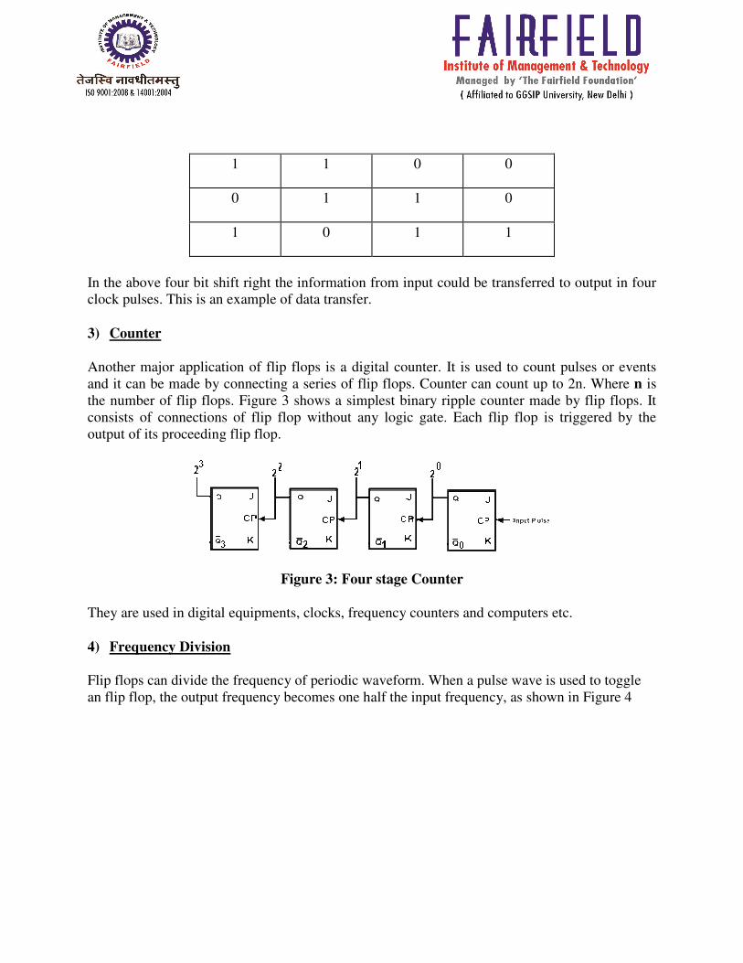
3) Counter
Another major application of flip flops is a digital counter. It is used to count pulses or events
and it can be made by connecting a series of flip flops. Counter can count up to 2n. Where n is
the number of flip flops. Figure 3 shows a simplest binary ripple counter made by flip flops. It
consists of connections of flip flop without any logic gate. Each flip flop is triggered by the
output of its proceeding flip flop.
Figure 3: Four stage Counter
They are used in digital equipments, clocks, frequency counters and computers etc.
4) Frequency Division
Flip flops can divide the frequency of periodic waveform. When a pulse wave is used to toggle
an flip flop, the output frequency becomes one half the input frequency, as shown in Figure 4

Figure 4: JK Flip Flop Used as A Frequency Division
The output of each flip flop is half the frequency of an input. If the input frequency is 160 KHz
then output of each flip flop would be so after first flip flop, 40 after second flip flop and 20 after
third flip flop.
Input frequency 160 KHz
Frequency of first flip flop 80 KHz
Frequency of 2nd flips flop 40 KHz
Frequency of 3rd flips flop 20 KHz
Shift Registers
A register is a device which is used to store information. Flip flops are often used to make a
register. Each flip flop can store 1-bit of information and therefore for storing a n-bit word n-flip-
flops are required in the register for example a computer employing 16-bit word length requires
16 flip-flops to hold the number before it is manipulated. The input to a register or output from it
may be either in serial or parallel form depending upon the requirement. If in these registers the
connection is done in such a way that the output of one of the flip flop forms in input to other, it
is known as a shift register. The data in a shift register is moved serially (one bit at a time). The
shift register can be built using RS, JK or D flip-flops.

Types of Shift Register:-
Serial-In Serial-Out
This configuration allows conversion from serial to Serial format. Data are input serially, and
once the data has been input, it received Serially at the Output.
Serial-In, Parallel-Out
This configuration allows conversion from serial to parallel format. Data are input
serially, and once the data has been input, it may be either read off at each output simultaneously,
or it can be shifted out and replaced.
Parallel-In, Serial-Out
This configuration has the data input in parallel format. To write the data to the
register, the Write/Shift control line must be held LOW. To shift the data, the control line is
brought HIGH and the registers are clocked. As long as the number of clock cycles is not more
than the length of the data-string, the Data Output, Q, will be the parallel data read off in order.
Parallel-In, Parallel-Out
This kind of shift register takes the data from the parallel inputs (D0-D3) and shifts it to the
corresponding output (Q0-Q3) when the registers are clocked. It can be used as a kind of
'history', retaining old information as the input in another part of the system, until ready for new
information, whereupon, the registers are clocked, and the new data are 'let through'

Bidirectional Shift Register
A bidirectional shift register is one which can do both the shift left and shift right operations. The
following steps are controlled by a clock sequentially. The lower register is the one in which the
data being shifted right or left. The upper register is being used as a temporary storage. The steps
are as follows.
1. The contents of the lower register are gated up directly to the upper register, which is
assumed to have been cleared previously. This is a parallel transfer of data and is
achieved by the first pulse or gate up pulse applied as the gate up terminals.
2. All the lower registers are reset i.e. set =0 by giving a pulse at the reset terminals.
3. The contents of the upper register are gate down to the lower register either one position
to the right or to the left as desired. This is again a parallel transfer of data.
4. The upper register is reset for the next shift operation.
UNIT -IV
Counters
COUNTERS
A counter is a device used to count operations, quantities, or periods of time. Counting is
frequently required in digital computers and other digital systems to record the number of events
occurring in a specified interval of time. Normally an electronic counter is used for counting the
number of pulses coming at the input line in a specified time period. The counter must possess
memory since it has to remember its past states. As with other sequential logic circuits counters
can be synchronous or asynchronous. As the name suggests, it is a circuit which counts. The
main purpose of the counter is to record the number of occurrence of some input. There are many
types of counter both binary and decimal. Commonly used counters are
1) Ripple counter
2) Synchronous Counter
3) Modulo Counters
4) Ring Counter
5) Twisted Ring Counter

1) Ripple counter:-
– The first flip-flop is clocked by the external clock pulse, and then each successive
flip-flop is clocked by the Q or Q' output of the previous flip-flop.
– But counters with states less than this number are also possible.
– They are designed to have the number of states in their sequences, which are
called truncated sequences.
– These sequences are achieved by forcing the counter to recycle before going
through all of its normal states.
2) Synchronous Counters - If all flip flops in the counter are triggered by a common clock
pulse, then the counter is called a "synchronous counter” and all memory elements are
simultaneously triggered by the same clock
Ring Counter
The ring counter is the simplest example of a shift register. The simplest counter is called a Ring
counter. The ring counter contains only one logical 1 or 0 which it circulates. The total cycle
length is equal to the number of stages. The ring counter is useful in applications where count
has to be recognized in order to perform some other logical operation. Since only one output is
ever at logic 1 at given time extra logic gates are not required to decode the counts and the flip
flop outputs may be used directly to perform the required operation.
Simple Ring Counter

Counter Truth Table
Clock 01 02 03 04
1 1 0 0 0
2 0 1 0 0
3 0 0 1 0
4 0 0 0 1
5 1 0 0 0
Johnson Counter (Twisted Ring counter)
A Johnson counter is a modified ring counter, where the inverted output from the last flip flop is
connected to the input to the first. The register cycles through a sequence of bit-patterns. The
MOD of the Johnson counter is 2n if n flip-flops are used. The main advantage of the Johnson
counter counter is that it only needs half the number of flip-flops compared to the standard ring
counter for the same MOD.
Modulo Counter:
A counter is a device which stores (and sometimes displays) the number of times a particular
event or process has occurred, often in relationship to a clock signal.
Decade counter ( Modulo Counter)

A circuit diagram of decade counter using JK FlipFlops (74LS112D)
A decade counter is one that counts in decimal digits, rather than binary. A decade counter may
have each digit binary encoded (that is, it may count in binary-coded decimal, as the 7490
integrated circuit did) or other binary encodings (such as the bi-quinary encoding of the 7490
integrated circuit). Alternatively, it may have a "fully decoded" or one-hot output code in which
each output goes high in turn (the 4017 is such a circuit). The latter type of circuit finds
applications in multiplexers and demultiplexers, or wherever a scanning type of behavior is
useful. Similar counters with different numbers of outputs are also common.
The decade counter is also known as a mod-counter when it counts to ten (0, 1, 2, 3, 4, 5, 6, 7, 8,
9). A Mod Counter that counts to 64 stops at 63 because 0 counts as a valid digit.
Primary Storage
RAM Memory
Random Access Memory (RAM) is the best known form of Computer Memory. The Read and
write (R/W) memory of a computer is called RAM. The User can write information to it and read
information from it. The RAM is a volatile memory; it means information written to it can be
accessed as long as power is on. As soon as the power is off, it cannot be accessed..RAM holds
data and processing instructions temporarily until the CPU needs it.
RAM is considered “random access” because we can access any memory cell directly if we
know the row and column that intersect at that cell.
There are two basic types of RAM :
(i) Dynamic Ram
(ii) Static RAM

Dynamic RAM : loses its stored information in a very short time (for milli sec.) even when
power supply is on. D-RAM’s are cheaper & lower.
Static RAM uses a completely different technology. S-RAM retains stored information only as
long as the power supply is on. Static RAM’s are costlier and consume more power. They have
higher speed than D-RAMs.
ROM Memory
Read only memory: Its non volatile memory, i.e, the information stored in it, is not lost even if
the power supply goes off. It’s used for the permanent storage of information. It also posses
random access property. Information can not be written into a ROM by the users/programmers.
In other words the contents of ROMs are decided by the manufactures.
The following types of ROMs an listed below :
(i) PROM : It’s programmable ROM. Its contents are decided by the user. The user can store
permanent programs, data etc in a PROM. The data is fed into it using a PROM programs.
(ii) EPROM : An EPROM is an erasable PROM. The stored data in EPROM’s can be erased by
exposing it to UV light for about 20 min. It’s not easy to erase it because the EPROM IC has to
be removed from the computer and exposed to UV light. The entire data is erased and not
selected portions by the user. EPROM’s are cheap and reliable.
(iii) EEPROM (Electrically Erasable PROM) : The chip can be erased & reprogrammed on
the board easily byte by byte. It can be erased with in a few milliseconds. There is a limit on the
number of times the EEPROM’s can be reprogrammed, i.e.; usually around 10,000 times.
Flash Memory : Its an electrically erasable & programmable permanent type memory. It uses
one transistor memory all resulting in high packing density, low power consumption, lower cost
& higher reliability. Its used in all power, digital cameras, MP3 players etc.
Programmable logic array (PLA):-

A programmable logic array (PLA) is a kind of programmable logic device used to implement
combinational logic circuits. The PLA has a set of programmable AND gate planes, which link
to a set of programmable OR gate planes, which can then be conditionally complemented to
produce an output.
Programmable Array Logic (PAL) is a family of programmable logic device semiconductors
used to implement logic functions in digital circuits introduced by Monolithic Memories. PAL
devices consisted of a small PROM (programmable read-only memory) core and additional
output logic used to implement particular desired logic functions with few components
References:-
1. www.ece.gmu.edu
2. www.uotechnology.edu
3. www.verticalhorizons.in
4. Morris Mano “Digital electronics”
5. R.P Jain “Modern Digital electronics”