subject-basic electronics engineering topic …
TRANSCRIPT

SUBJECT-BASIC ELECTRONICS ENGINEERING
TOPIC-SEMICONDUCTOR DIODE
Prepared by Mr. Bikash Meher
Assistant Professor
Department-EE
Topic includes
Construction and operation of p-n Junction Diode
Construction and operation Rectifier

2
Semiconductor Diode and Its Applications
1. P-N JUNCTION DIODE
A p-n junction is formed by joining p-type and n-type semiconductors together in very close
contact. The term junction refers to the boundary interface where the two regions of the
semiconductor meet. If they were constructed of two separate pieces this would introduce a
grain boundary, so p-n junctions are created in a single crystal of semiconductor by doping, for
example, by ion implantation, diffusion of dopants, or by epitaxy (growing a layer of crystal
doped with one type of dopant on top of a layer of crystal doped with another type of dopant).
p-n junctions are elementary “building blocks” of almost all semiconductor electronic devices
such as diodes, transistors, solar cells, LEDs, and integrated circuits. The regions near by the
p-n interfaces lose their neutrality and become charged, forming the space charge region or
depletion layer
Fig.1. A p-n junction in thermal equilibrium with zero bias voltage applied
The electric field created by the space charge region opposes the diffusion process for both
electrons and holes. There are two concurrent phenomena: the diffusion process that tends to
generate more space charge, and the electric field generated by the space charge that tends to
counteract the diffusion. The carrier concentration profile at equilibrium is shown in Fig.1. The
space charge region is a zone with a net charge provided by the fixed ions (donors or acceptors)
that have been left uncovered by majority carrier diffusion. When equilibrium is reached, the
charge density is approximated by the displayed step function. In fact, the region is completely
depleted of majority carriers (leaving a charge density equal to the net doping level), and the

3
Semiconductor Diode and Its Applications
edge between the space charge region and the neutral region is quite sharp. The space charge
region has the same charge on both sides of the p-n interfaces, thus it extends farther on the
less doped side.
2. FORWARD BIASING AND REVERSE BIASING
Forward Biasing:
When external voltage applied to the junction is in such a direction that it cancels the potential barrier, thus
permitting current flow is called forward biasing. To apply forward bias, connect +ve terminal of the battery
to p-type and –ve terminal to n-type as shown in Fig. 2. The applied forward potential establishes the electric
field which acts against the field due to potential barrier. Therefore, the resultant field is weakened and the
barrier height is reduced at the junction as shown in Fig. 2.2. Since the potential barrier voltage is very small,
a small forward voltage is sufficient to completely eliminatethe barrier. Once the potential barrier is
eliminated by the forward voltage, junction resistance becomes almost zero and a low resistance path is
established for the entire circuit. Therefore, current flows in the circuit. This is called forward current.
Fig. 2. Forward biasing of p-n junction
Reverse Biasing
When the external voltage applied to the junction is in such a direction the potential barrier is increased it is
called reverse biasing. To apply reverse bias, connect –ve terminal of the battery to p-type and +ve terminal
to n-type as shown in Fig.3. The applied reverse voltage establishes an electric field which acts in the same
direction as the field due to potential barrier. Therefore, the resultant field at the junction is strengthened and
the barrier height is increased as shown in Fig.3. The increased potential barrier prevents the flow of charge
carriers across the junction. Thus, a high resistance path is established for the entire circuit and hence current
does not flow.

4
Semiconductor Diode and Its Applications
Fig. 3. Reverse biasing of p-n junction
3. VOLT-AMPERE (V-I ) CHARACTERISTICS OF P-N JUNCTION
DIODE The V-I characteristics of a semiconductor diode can be obtained with the help of the circuit
shown in Fig. 4 (i). The supply voltage V is a regulated power supply, the diode is forward
biased in the circuit shown. The resistor R is a current limiting resistor. The voltage across the
diode is measured with the help of voltmeter and the current is recorded using an ammeter. By
varying the supply voltage different sets of voltage and currents are obtained. By plotting these
values on a graph, the forward characteristics can be obtained. It can be noted from the graph
the current remains zero till the diode voltage attains the barrier potential. For silicon diode,
the barrier potential is 0.7 V and for germanium diode, it is 0.3 V. The barrier potential is also
called knee voltage or cut-in voltage. The reverse characteristics can be obtained by reverse
biasing the diode. It can be noted that at a particular reverse voltage, the reverse current
increases rapidly. This voltage is called breakdown voltage.

5
Semiconductor Diode and Its Applications
Fig. 4 V-I characteristics of p-n junction diode (i) circuit diagram; (ii) charactristics
4. DIODE CURRENT EQUATION

6
Semiconductor Diode and Its Applications
5. DIODE EQUIVALENT CIRCUIT
Fig. 5. Diode equivalent circuit. (i) Symbol (ii) equivalent circuit
The forward current If flowing through the diode causes a voltage drop in its internal resistance,
rf. Therefore, the forward voltage VF applied across the actual diode has to overcome
1. potential barrier Vo
2. internal drop If rf
Vf = Vo + If rf
For silicon diode Vo = 0.7 V whereas for germanium diode Vo = 0.3 V.
For ideal diode rf = 0.
Basic Definitions
Knee Voltage or Cut-in Voltage
It is the forward voltage at which the diode starts conducting.
Breakdown Voltage
It is the reverse voltage at which the diode (p-n junction) breaks down with a sudden rise in
reverse current.
Peak-inverse Voltage (PIV)
It is the maximum reverse voltage that can be applied to a p-n junction without causing damage
to the junction. If the reverse voltage across the junction exceeds its peak inverse voltage, then
the junction exceeds its peak-inverse voltage, and the junction gets destroyed because of
excessive heat.

7
Semiconductor Diode and Its Applications
Maximum Forward Current
It is the maximum instantaneous forward current that a p-n junction can conduct without
damaging the junction. If the forward current is more than the specified rating then the junction
gets destroyed due to overheating.
6. VOLT-AMPERE (V-I) C HARACTERISTICS OF IDEAL DIODE
Diode permits only unidirectional conduction. It conducts well in forward direction and poorly
in reverse direction. It would have been ideal if a diode acted as a perfect conductor (with zero
voltage across it) when forward-biased, and as a perfect insulator (with no current through it)
when reverse-biased. The V-I characteristics of such an ideal diode would be as shown in Fig.
6. An ideal diode acts like an automatic switch. When the current tries to flow in the forward
direction, the switch is closed. On the other hand, when the current tries to flow in the reverse
direction, the switch is open.
Fig. 6.
7. STATIC AND DYNAMIC RESISTANCE OF A DIODE
DC or Static Resistance
When diode is forward biased, it offers a definite resistance in the circuit. This resistance is known as dc
resistance or static resistance (RF). It is simply the ratio of the dc voltage (VD) across the diode to the dc
current (ID) flowing through it as shown in Fig.7.

8
Semiconductor Diode and Its Applications
Fig. 7. Determination of dc resistance of a diode at a specific operating point
AC or Dynamic Resistance
The ac or dynamic resistance of a diode, at a particular dc voltage, is equal to the reciprocal of the slope of
the characteristics at that point, as shown in Fig. 8.
ΔVD= change in voltage
ΔID= change in current

9
Semiconductor Diode and Its Applications
Fig. 8. Determination of ac resistance of a diode at a specific operating point

10
Semiconductor Diode and Its Applications
8. HALF-WAVE RECTIFIER The circuit diagram of a half-wave rectifier is shown in Fig. 9 along with the I/P and O/P
waveforms.
Fig. 9
The transformer is employed in order to step-down the supply voltage and also to prevent from
shocks. The diode is used to rectify the ac signal while the pulsating dc is taken across the load
resistor RL. During the +ve half-cycle, the end X of the secondary is +ve and end Y is –ve.
Thus, forward biasing the diode. As the diode is forward biased, the current flows through the
load RL and a voltage is developed across it. During the –ve half-cycle the end Y is +ve and
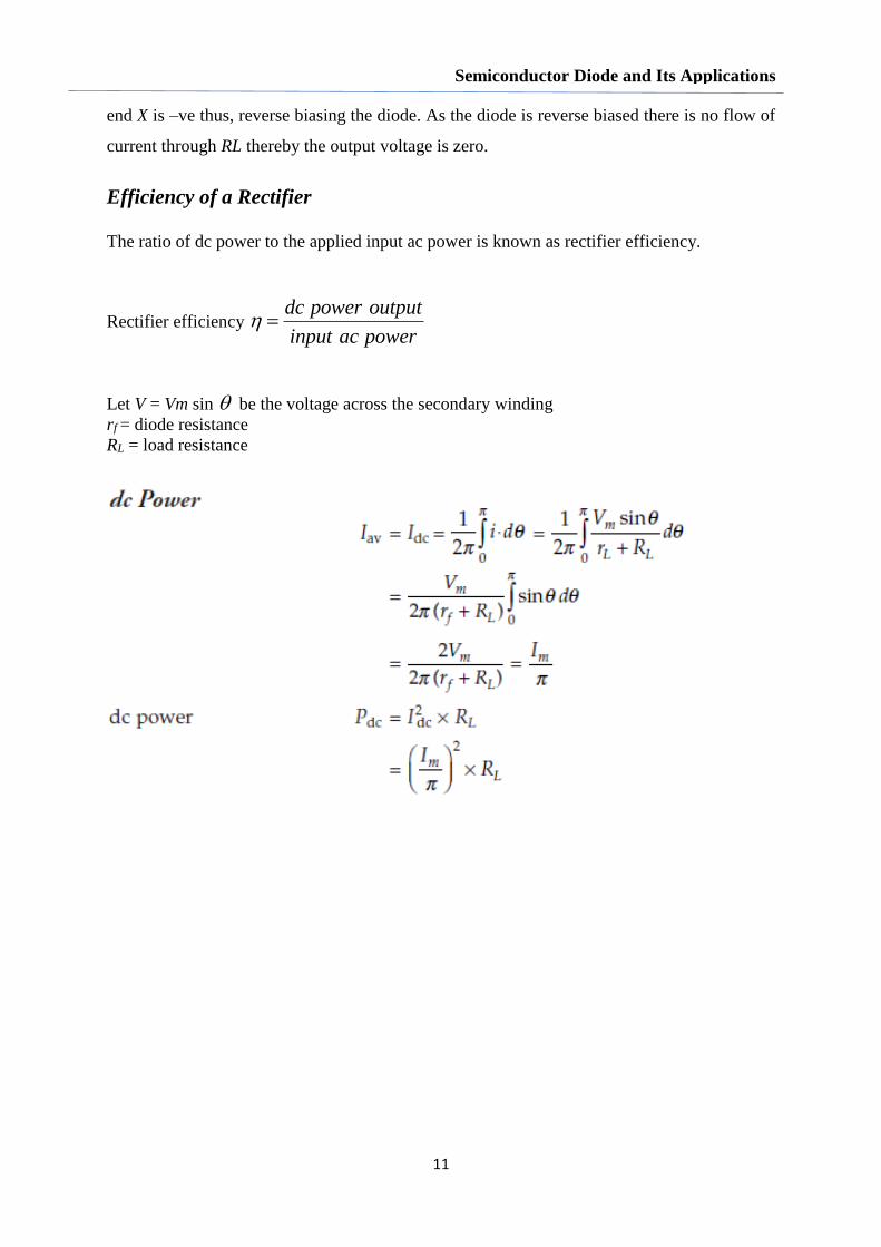
11
Semiconductor Diode and Its Applications
end X is –ve thus, reverse biasing the diode. As the diode is reverse biased there is no flow of
current through RL thereby the output voltage is zero.
Efficiency of a Rectifier The ratio of dc power to the applied input ac power is known as rectifier efficiency.
Rectifier efficiency dc power output
input ac power
Let V = Vm sin be the voltage across the secondary winding
rf = diode resistance
RL = load resistance

12
Semiconductor Diode and Its Applications
9. FULL-WAVE RECTIFIER
Full wave Rectifier of two types
(i) Centre tapped full-wave rectifier
(ii) Bridge fullwave rectifier
(i) Centre tapped full-wave rectifier
The circuit diagram of a centre tapped full-wave rectifier is shown in Fig. 10. It employs two
diodes and a centre tap transformer. The ac signal to be rectified is applied to the primary of
the transformer and the dc output is taken across the load, RL. During the +ve half-cycle end X
is +ve and end Y is –ve. This makes diode D1 forward biased and thus a current i1 flows through

13
Semiconductor Diode and Its Applications
it and load resistor RL. Diode D2 is reverse biased and the current i2 is zero. During the –ve
half-cycle end Y is +ve and end X is –ve. Now diode D2 is forward biased and thus a current i2
flows through it and load resistor RL. Diode D1 is reversed and the current i1 = 0.
Fig.10. Centre tapped full-wave rectifier (i) circuit diagram; (ii) input and output waveforms
(ii) Bridge rectifier
The circuit diagram of a bridge rectifier is shown in Fig. 11. It uses four diodes and one
transformer.
During the +ve half-cycle, end A is +ve and end B is –ve thus diodes D1 and D3 are forward
bias while diodes D2 and D4 are reverse biased thus a current flows through diode D1, load RL
(C to D) and diode D3.
During the –ve half-cycle, end B is +ve and end A is –ve thus diodes D2 and D4 are forward
biased while the diodes D1 and D3 are reverse biased. Now the flow of current is through diode
D4 load RL (D to C) and diode D2. Thus, the waveform is same as in the case of centre-tapped
full-wave rectifier.

14
Semiconductor Diode and Its Applications
(ii)
Fig. 11. Centre tapped full-wave rectifier (i) circuit diagram; (ii) output waveform
Efficiency of full-wave rectifier

15
Semiconductor Diode and Its Applications
The efficiency will be maximum if rf is negligible as compared to RL.
Hence, maximum efficiency = 81.2%
This is double the efficiency due to half-wave rectifier. Therefore, a full-wave rectifier is
twice as effective as a half-wave rectifier.

16
Semiconductor Diode and Its Applications
Ripple Factor
The pulsating output of a rectifier consists of dc component and ac component (also known as
ripple). The effectiveness of a rectifier depends on the magnitude of ac component in the output
: the smaller this component, the more effective is the rectifier.
Ripple factor (r) is defined as it is the ratio of rms value of ac component to the dc component
in the rectifier output.
ac
dc
Ir
I
Ripple Factor for halfwave rectifier
By definition the effective (i.e., rms) value of total load current is given by
2 2 2
ac dcrmsI I I
2 2
ac dcrmsI I I
where Idc = value of dc component
Iac = rms value of ac component
Divide both RHS and LHS by Idc, we get
2 21acrms dc
dc dc
II I
I I
2
1rms
dc
Ir
I
For half-wave rectification, 2
mrms
II and m
dc
II
So, the ripple factor (r) of half-wave rectifier is 1.21.
Ripple Factor for Full-wave Rectification
For full-wave rectification,
2
mrms
II and
2 mdc
II
So, the ripple factor (r) of full-wave rectifier is 0.48.

17
Semiconductor Diode and Its Applications
10. COMPARISON OF RECTIFIERS


SUBJECT-BASIC ELECTRONICS ENGINEERING
TOPIC-BIPOLAR JUNCTION TRANSISTOR
Prepared by Mr. Bikash Meher
Assistant Professor
Department-EE

2
Bipolar Junction Transistor
Bipolar Junction Transistor
(BJT)
A bipolar junction transistor is a three layer semiconductor device which is consisting of two
P layer and a N layer or two N layer with a P layer. A N layer is sandwiched between two P
layer known as PNP transistor and similarly, if a P layer is sandwich between two N layer
called as NPN transistor. The BJT consists of three terminal named as base (B), emitter (E) and
collector (C).
Fig.1. PNP and NPN transistor.
Fig. 2. Symbol of BJT: (a) PNP; (b) NPN.
The width and doping level of the base, emitter and collector are compares as:
Width: Base < Emitter < Collector
Doping : Emitter > Collecor > Base
The width of the collector layer is large as compared to based and emitter and the doping is
high in emitter layer as compared to other two . The abbreviation BJT, from bipolar junction
transistor, is often applied to this three-terminal device. The term bipolar reflects the fact that
holes and electrons participate in the injection process into the oppositely polarized material.

3
Bipolar Junction Transistor
TRANSISTOR OPERATION
The basic arrangement with different bias volatge for npn and pnp transistor is shown in Fig.
4. Now, we will describe the operation of the pnp transistor as per the diagram depicted in Fig.
4a .The operation of the npn transistor is exactly the same if the roles played by the electron
and hole are interchanged. In Fig.5a the pnp transistor has been redrawn without the base-to
collector bias. This is similar to the forward biasing of p-n junction diode. The depletion region
has been reduced in width due to the applied bias, resulting in a heavy flow of majority carriers
from the p - to the n -type material.
Let us now remove the base-to-emitter bias of the pnp transistor of Fig. 4a as shown in Fig. 5b
. This is similar to the forward biasing of p-n junction diode. The depletion region has been
expand in width due to the reverse bias voltage. The flow of majority carriers is zero, resulting
in only a minority carriers flow.
Fig. 4. Types of transistor: (a) pnp; (b) npn
+
+
+
-
+-
+-
+
- +
+ - +
+-
-
-
-
-
-
E
B
C
VEE
Depletion
region
Majority carriers
+ -
+
+
+-
+ -
+ -
+
-+
+-
+
+-
-
-
-
-
-
E
B
C
Minority carriers
+ -
+
+
+ +
Depletion
region
+ -VCC
p n
np
+
+
+
-
+-
+-
+
- +
+ - +
+-
-
-
-
-
-
E
B
C
VEE
Depletion
region
Majority carriers
+ -
+
+
+-
+ -
+ -
+
-+
+-
+
+-
-
-
-
-
-
E
B
C
Minority carriers
+ -
+
+
+ +
Depletion
region
+ -VCC
p n
np
(a) (b)
Fig. 5. Biasing of a transistor: (a) forward biased; (b) reverse biased.

4
Bipolar Junction Transistor
Fig. 6. Majority and minority carrier flow of a pnp transistor.
In Fig.6 both biasing potentials have been applied to a pnp transistor, with the resulting
majority- and minority-carrier flows indicated. As indicated in Fig.6 , a large number of
majority carriers will diffuse across the forward biased p–n junction into the n -type material.
Since the sandwiched n -type material is very thin and has a low conductivity, a very small
number of these carriers will take this path of high resistance to the base terminal. The
magnitude of thebase current is typically on the order of microamperes, as compared to
milliamperes for theemitter and collector currents. The larger number of these majority carriers
will diffuse acrossthe reverse-biased junction into the p -type material connected to the
collector terminal as indicatedin Fig.6 . All the minority carriers in the depletion region will
cross the reverse-biased junction of a diode accounts for the flow indicated in Fig.6 .
Applying Kirchhoff’s current law to the transistor of Fig.6 as if it were a single
node,we obtain
IE = IC + IB
So, emitter current is the sum of the collector and base currents.
The collector current, however, comprises two components–the majority and the minority
carriers as indicated in Fig. 6 . The minority-current component is called the leakage current
and is given the symbol ICO (IC current with emitter terminal open). The collector current,
therefore, is determined in total by
IC = ICmajority + ICOminority
IC is measured in milliamperes and ICO is measured in microamperes or nanoamperes. ICO ,
like Is for a reverse-biased diode.

5
Bipolar Junction Transistor
COMMON-BASE CONFIGURATION
The common base configuration with pnp and npn transistors is shown in Fig. 7. The common-
base terminology is derived from the fact that the base is common to both the input and output
sides of the configuration. In addition, the base is usually the terminal closest to, or at, ground
potential. The arrow in the graphic symbol defines the direction of emitter current
(conventional flow) through the device.
Fig. 7. Common base configuration: (a) pnp transistor; (b) npn transistor
Input Characteristics
The input charactristics of the common base transistor configuration is depicted in Fig.8. The
input set for the common-base amplifier as shown in Fig. 8 relates an input current (IE) to an
input voltage (VBE) for various levels of output voltage (VCB). The input characteristics of Fig.8
reveal that for fixed values of collector voltage (VCB), as the base-to-emitter voltage increases,
the emitter current increases in a manner that closely resembles the diode characteristics. In
fact, increasing levels of VCB have such a small effect on the characteristics that as a first
approximation the change due to changes in VCB can be ignored. once a transistor is in the “on”
state, the base-to-emitter voltage will be assumed to be the following:
0.7BEV V

6
Bipolar Junction Transistor
Fig. 8. Input characteristics of common base silicon amplifier.
Output Characteristics
The output set relates an output current (IC) to an output voltage (VCB) for various levels of
input current (IE) as shown in Fig. 9 . The output or collector set of characteristics has three
basic regions of interest, as indicated in Fig. 9 : the active , cutoff , and saturation regions. The
active region is the region normally employed for linear (undistorted) amplifiers.
Fig. 9. Output characteristics of common base silicon amplifier.

7
Bipolar Junction Transistor
In particular:
In the active region the base–emitter junction is forward-biased, whereas the collector base
junction is reverse-biased.
The active region is defined by the biasing arrangements of Fig. 7. At the lower end of the
active region the emitter current (IE) is zero, and the collector current is simply that due to the
reverse saturation current ICO , as indicated in Fig.10. The current ICO is so small
(microamperes) in magnitude compared to the vertical scale of IC (milliamperes) that it appears
on virtually the same horizontal line as IC = 0. The circuit conditions that exist when IE =0 for
the common-base configuration are shown in Fig.10.
Fig. 10. Reverse saturation current
From the Fig. 9, it is seen that as the emitter current increases above zero, the collector current
increases to a magnitude essentially equal to that of the emitter current as determined by the
basic transistor-current relations. Note also the almost negligible effect of VCB on the collector
current for the active region. The curves clearly indicate that a first approximation to the
relationship between IE and IC in the active region is given by
C EI I
As inferred by its name, the cutoff region is defined as that region where the collector current
is 0 A, as revealed on Fig. 9 . In addition:
In the cutoff region the base–emitter and collector–base junctions of a transistor are both
reverse-biased.
The saturation region is defined as that region of the characteristics to the left of VCB = 0 V.
The horizontal scale in this region was expanded to clearly show the dramatic change in

8
Bipolar Junction Transistor
characteristics in this region. Note the exponential increase in collector current as the voltage
VCB increases toward 0 V.
In the saturation region the base–emitter and collector–base junctions are forward-biased.
Alpha (α)
DC Mode In the dc mode the levels of IC and IE due to the majority carriers are related by a
quantity called alpha and defined by the following equation: where IC and IE are the levels of
current at the point of operation.
COMMON-EMITTER CONFIGURATION
The common emitter configuration is shown in Fig.11. It is called the common-emitter
configuration because the emitter is common to both the input and output terminals (in this
case common to both the base and collector terminals).
Input Characteristics
The input characteristics of the common-emitter configuration is shown in Fig. 12b. In common
base that the input set of characteristics was approximated by a straight-line equivalent that
resulted in VBE =0.7 V for any level of IE greater than 0 mA. For the common-emitter
configuration the same approach can be taken,resulting in the approximate equivalent of Fig.
12b. The result supports our earlier conclusion that for a transistor in the “on” or active region
the base-to-emitter voltage is 0.7 V. In this case the voltage is fixed for any level of base
current.

9
Bipolar Junction Transistor
Fig.11. Notation and symbols used with the common-emitter configuration: (a) npn
transistor; (b) pnp transistor.
Fig. 12. Characteristics of a silicon transistor in the common-emitter configuration: (a) output
characteristics; (b) input characteristics.

10
Bipolar Junction Transistor
Output Characteristics
For the common-emitter configuration the output characteristics are a plot of the output current
(IC) versus output voltage (VCE) for a range of values of input current (IB). The input
characteristics are a plot of the input current (IB) versus the input voltage (VBE) for a range of
values of output voltage (VCE). The output characteristics of common-emitter is illustrated in
Fig. 12a.
The active region for the common-emitter configuration is that portion of the upper-right
quadrant that has the greatest linearity, that is, that region in which the curves for IB are nearly
straight and equally spaced. In Fig. 12a this region exists to the right of the vertical dashed line
at V CE sat and above the curve for IB equal to zero. The region to the left of VCE sat is called the
saturation region.
In the active region of a common-emitter amplifier, the base–emitter junction is forward-
biased, whereas the collector–base junction is reverse-biased.
The cutoff region for the common-emitter configuration is not as well defined as for the
common-base configuration. Note on the collector characteristics of Fig.12a that IC is not equal
to zero when IB is zero. A small current exist even if the IB = 0 as illustarated in Fig.13. For the
common-base configuration, when the input current IE was equal to zero, the collector current
was equal only to the reverse saturation current ICO , so that the curve IE =0 and the voltage
axis were, for all practical purposes, one.
Fig.13 Circuit condition related to ICEO.
From the common base characteristics
11
Bipolar Junction Transistor
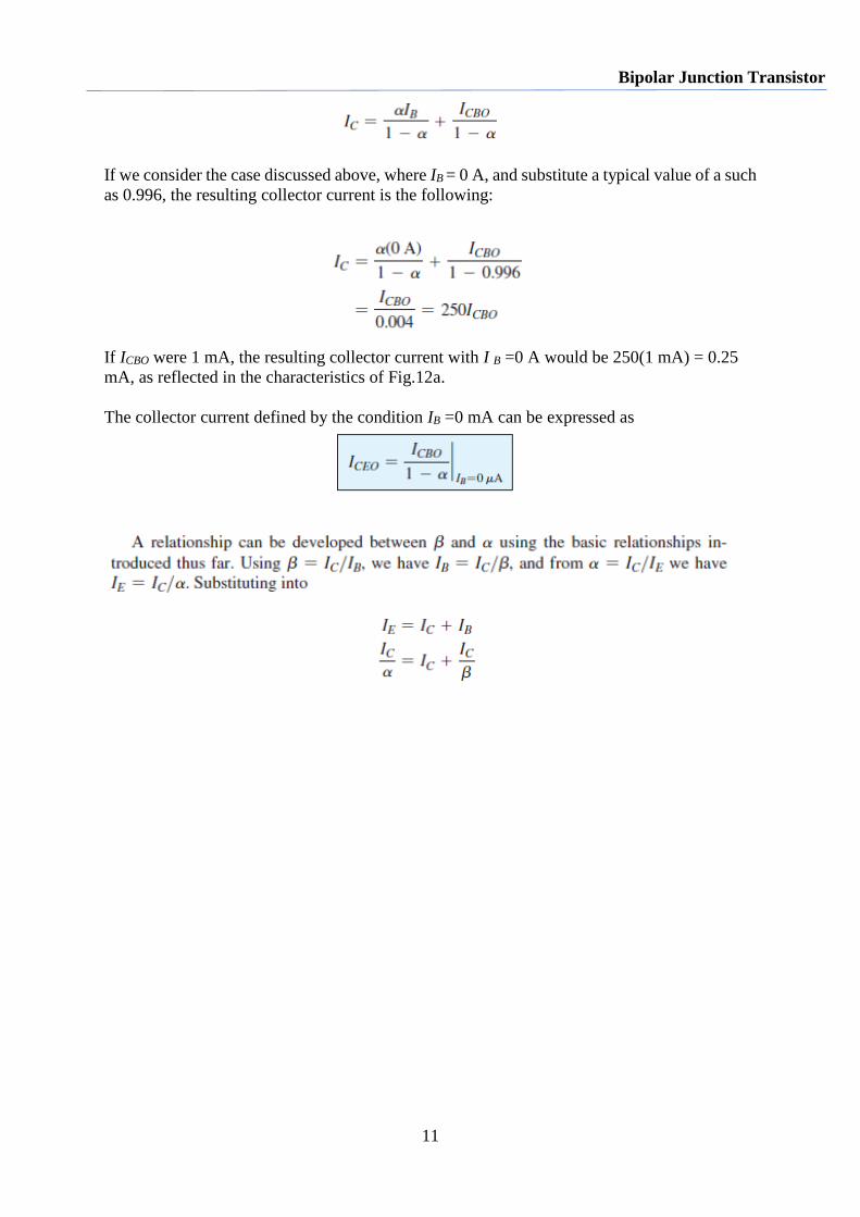
If we consider the case discussed above, where IB = 0 A, and substitute a typical value of a such
as 0.996, the resulting collector current is the following:
If ICBO were 1 mA, the resulting collector current with I B =0 A would be 250(1 mA) = 0.25
mA, as reflected in the characteristics of Fig.12a.
The collector current defined by the condition IB =0 mA can be expressed as

12
Bipolar Junction Transistor
`
Equations

13
Bipolar Junction Transistor

SUBJECT-BASIC ELECTRONICS ENGINEERING
TOPIC-FIELD EFFECT TRANSISTOR
Prepared by Mr. Bikash Meher
Assistant Professor
Department-EE
Topic includes
Construction and operation of JFET
Construction and operation of D-MOSFET
Construction and operation of E-MOSFET

2
Field Effect Transistor
FIELD EFFECT TRANSISTOR (FET)
There are three types of FETs: JFETs, MOSFETs, and MESFETs. Further, MOSFETs are
classified into depletion type and enhancement-type (D-MOSFET and E-MOSFET).
1. JUNCTION FIELD-EFFECT TRANSISTOR (JFET)
The field-effect transistor (FET) is a three-terminal device.The three terminals are gate(G),
source (S) and Ddrain (D).The FET is voltage controlled device. Just as there are npn and pnp
bipolar transistors, there are n-channel and p-channel field effect transistors.
The term field effect in the name deserves some explanation. For the FET an electric
field is established by the charges present, which controls the conduction path of the output
circuit without the need for direct contact between the controlling and controlled quantities.
FETs are of three types : the junction field-effect transistor (JFET), the metal–oxide–
semiconductor field-effect transistor (MOSFET), and the metal – semiconductor field-effect
transistor (MESFET). The MOSFET category is further broken down into depletion and
enhancement ( i.e. D-MOSFET and E=MOSFET).
Difference between BJT and FET
BJT FET
Current controlled device Voltage controlled device
Bipolar (current conduction due to flow of
holes and electrons)
Uniploar (current conduction due to flow of
majority charge carriers)
Low input impedance as compared to FET High input impedance
Ac voltage gain is high Ac voltage gain is low
Less temperature stable More temperature stable
Larger in size Smaller in size
Construction and Characteristics of JFET

3
Field Effect Transistor
The basic construction of the n -channel JFET is shown in Fig.1. major part of the structure is
the n -type material, which forms the channel between the embedded layers of p -type material.
The top of the n -type channel is connected through an ohmic contact to a terminal referred to
as the drain (D) , whereas the lower end of the same material is connected through an ohmic
contact to a terminal referred to as the source (S). The two p -type materials are connected
together and to the gate (G) terminal. In essence, therefore, the drain and the source are
connected to the ends of the n -type channel and the gate to the two layers of p -type material.
Operation of JFET
In the absence of any applied potentials the JFET has two p – n junctions under no-bias
conditions. The result is a depletion region at each junction, as shown in Fig. 1 , that resembles
the same region of a diode under no-bias conditions. So, depletion region is void of free carriers
and is therefore unable to support conduction.
Fig 1. Junction field effect transistor (JFET)
VGS = 0 V, VDS Some Positive Value
In Fig. 2 , a positive voltage VDS is applied across the channel and the gate is connected directly
to the source to establish the condition VGS = 0 V. The result is a gate and a source terminal at
the same potential and a depletion region in the low end of each p –material similar to the

4
Field Effect Transistor
distribution of the no-bias conditions of Fig. 1 . The instant the voltage VDD (=VDS) is applied,
the electrons are drawn to the drain terminal, establishing the conventional current ID with the
defined direction of Fig. 2 . The path of charge flow clearly reveals that the drain and source
currents are equivalent (ID = IS). Under the conditions in Fig. 2 , the flow of charge is relatively
uninhibited and is limited solely by the resistance of the n -channel between drain and source.
It is seen that the depletion region is wider near the top of both p –type materials. The
reason for the change in width of the region is best described through the help of Fig. 3 .
Assuming a uniform resistance in the n -channel, we can break down
Fig. 2. JFET at VGS=0V and VDS>0V Fig.3 Varying reverse-bias potential across the
p-n juction of an n-channel JFET
the resistance of the channel into the divisions appearing in Fig. 3 . The current ID will establish
the voltage levels through the channel as indicated on the same figure. The result is that the
upper region of the p -type material will be reverse-biased by about 1.5 V, with the lower region
only reverse-biased by 0.5 V. The greater the applied reverse bias, the wider is the depletion
region—hence the distribution of the depletion region as shown in Fig. 3 . The fact thatthe p –
n junction is reversebiased for the length of the channel results in a gate current of zero amperes,
as shown in the same figure.
As the voltage VDS is increased from 0 V to a few volts, the current will increase as
determined by Ohm’s law and the plot of ID versus VDS will appear as shown in Fig. 4 .

5
Field Effect Transistor
Fig. 4. ID versus VDS for VGS=0V
The relative straightness of the plot reveals that for the region of low values of VDS , the
resistance is essentially constant. As VDS increases and approaches a level referred to as VP in
Fig. 4 , the depletion regions of Fig. 2 will widen, causing a noticeable reduction in the channel
width. The reduced path of conduction causes the resistance to increase and the curve in the
graph of Fig. 4 to occur. The more horizontal the curve, the higher the resistance, suggesting
that the resistance is approaching “infinite” ohms in the horizontal region. If VDS is increased
to a level where it appears that the two depletion regions would “touch” as shown in Fig. 5 , a
condition referred to as pinch-off will result. The level of VDS that establishes this condition is
referred to as the pinch-off voltage and is denoted by VP , as shown in Fig. 4 .

6
Field Effect Transistor
Fig. 5. Pinch-off (VGS=0V, VDS=VP)
In actuality, the term pinch-off is a misnomer in that it suggests the current ID is pinched off
and drops to 0 A. As shown in Fig.4, however, this is hardly the case – ID maintains a saturation
level defined as IDSS in Fig. 4 . In reality a very small channel still exists, with a current of very
high density. The fact that ID does not drop off at pinch-off and maintains the saturation level
indicated in Fig. 4 is verified by the following fact: The absence of a drain current would
remove the possibility of different potential levels through the n - channel material to establish
the varying levels of reverse bias along the p – n junction. The result would be a loss of the
depletion region distribution that caused pinch-off in the first place.
As VDS is increased beyond VP , the region of close encounter between the two depletion
regions increases in length along the channel, but the level of ID remains essentially the same.
In essence, therefore, once VDS > VP , the JFET has the characteristics of a current source. As
shown in Fig. 6 , the current is fixed at ID = IDSS, but the voltage VDS (for levels >VP ) is
determined by the applied load.

7
Field Effect Transistor
Fig.6 Current source equivalent for VGS=0V, VDS>VP.
The choice of notation IDSS is derived from the fact that it is the drain-to- source current with a
short-circuit connection from gate to source. As we continue to investigate the characteristics
of the device we will find that:
IDSS is the maximum drain current for a JFET and is defined by the conditions VGS = 0 V
and VDS >|VP|.
V GS < 0 V
The voltage from gate to source, denoted VGS, is the controlling voltage of the JFET. Just as
various curves for IC versus VCE were established for different levels of IB for the BJT transistor,
curves of ID versus VDS for various levels of V GS can be developed for the JFET. For the n -
channel device the controlling voltage VGS is made more and more negative from its VGS = 0 V
level. In other words, the gate terminal will be set at lower and lower potential levels as
compared to the source.

8
Field Effect Transistor
Fig.7. Application of anegative voltage to the gate of a JFET.
In Fig. 7 a negative voltage of –1 V is applied between the gate and source terminals for a low
level of VDS . The effect of the applied negative-bias VGS is to establish depletion regions similar
to those obtained with V GS = 0 V, but at lower levels of VDS . Therefore, the result of applying
a negative bias to the gate is to reach the saturation level at a lower level of VDS , as shown in
Fig. 8 for VGS = -1 V.

9
Field Effect Transistor
Fig. 8.n- Channel JFET charactristics with IDSS=8mA and VP=–4 V.
The resulting saturation level for ID has been reduced and in fact will continue to decrease as
VGS is made more and more negative. The pinch-off voltage continues to drop in a parabolic
manner as VGS becomes more and more negative. Eventually, VGS when VGS = -VP will be
sufficiently negative to establish a saturation level that is essentially 0 mA, and the device has
been “turned off.”
The level of VGS that results in ID = 0 mA is defined by VGS =VP, with VP being a negative
voltage for n-channel devices and a positive voltage for p-channel JFETs.
Fig. 9. JFET symbols: (a)n-channel; (b)p-channel.

10
Field Effect Transistor
2. MOSFET
MOSFET stands for metal – oxide – emiconductor field – effect transistor. MOSFETs are
further broken down into depletion type and enhancement type. The terms depletion and
enhancement define their basic mode of operation.
2.1 DEPLETION-TYPE MOSFET (D-MOSFET)
Basic Construction
The basic construction of the n -channel depletion-type MOSFET is provided in Fig. 10. A slab
of p -type material is formed from a silicon base and is referred to as the substrate. It is the
foundation on which the device is constructed. In some cases the substrate is internally
connected to the source terminal. However, many discrete devices provide an additional
terminal labeled SS , resulting in a four-terminal device. The source and drain terminals are
connected through metallic contacts to n -doped regions linked by an n -channel as shown in
the figure. The gate is also connected to a metal contact surface but remains insulated from the
n -channel by a very thin silicon dioxide (SiO2 ) layer. SiO2 is a type of insulator referred to as
a dielectric , which sets up opposing (as indicated by the prefix di -) electric fields within the
dielectric when exposed to an externally applied field. The fact that the SiO2 layer is an
insulating layer means that:
There is no direct electrical connection between the gate terminal and the channel of a
MOSFET.

11
Field Effect Transistor
Fig.10. n-Channel depletion type MOSFET.
In addition:
It is the insulating layer of SiO 2 in the MOSFET construction that accounts for the very
desirable high input impedance of the device.
The reason for the label metal–oxide–semiconductor FET is now fairly obvious: metal for the
drain, source, and gate connections; oxide for the silicon dioxide insulating layer; and
semiconductor for the basic structure on which the n - and p -type regions are diffused.

12
Field Effect Transistor
Basic Operation and Characteristics
In Fig. 11, the gate-to-source voltage is set to 0 V by the direct connection from one terminal
to the other, and a voltage VDD is applied across the drain-to-source terminals. The result is an
attraction of the free electrons of the n-channel for the positive voltage at the drain. The result
is a current similar to that flowing in the channel of the JFET. In fact, the resulting current with
VGS =0 V continues to be labeled IDSS , as shown in Fig. 12 .
Fig. 11. N-channel depletion type MOSFET with VGS=0V and applied voltage VDD.
In Fig. 12 , VGS is set at a negative voltage such as –1 V. The negative potential at the gate will
tend to pressure electrons toward the p -type substrate (like charges repel) and attract holes
from the p -type substrate (opposite charges attract) as shown in Fig. 12 . Depending on the
magnitude of the negative bias established by VGS , a level of recombination between electrons
and holes will occur that will reduce the number of free electrons in the n -channel available
forconduction. The more negative the bias, the higher is the rate of recombination.

13
Field Effect Transistor
Fig. 12. Reduction in free carriers in a channel due to a negative potential
at the gate terminal.
The resulting level of drain current is therefore reduced with increasing negative bias for VGS ,
as shown in Fig. 13 for VGS = -1 V, -2 V, and so on, to the pinch-off level of -6 V. The resulting
levels of drain current and the plotting of the transfer curve proceed exactly as described for
the JFET.
Fig. 13. Drain and transfer characteristics for an n-channel depletion type MOSFET.

14
Field Effect Transistor
For positive values of VGS , the positive gate will draw additional electrons (free carriers) from
the p -type substrate due to the reverse leakage current and establish new carriers through the
collisions resulting between accelerating particles. As the gate-to-source voltage continues to
increase in the positive direction, Fig.13 reveals that the drain current will increase at a rapid
rate for the reasons listed above. The vertical spacing between the VGS =0 V and VGS = +1 V
curves of Fig. 13 is a clear indication of how much the current has increased for the 1-V change
in VGS . Due to the rapid rise, the user must be aware of the maximum drain current rating since
it could be exceeded with a positive gate voltage. That is, for the device of Fig. 13, the
application of a voltage VGS = +4 V would result in a drain current of 22.2 mA, which could
possibly exceed the maximum rating (current or power) for the device. As revealed above, the
application of a positive gate-to-source voltage has “enhanced” the level of free carriers in the
channel compared to that encountered with VGS = 0 V. For this reason the region of positive
gate voltages on the drain or transfer characteristics is often referred to as the enhancement
region , with the region between cutoff and the saturation level of IDSS referred to as the
depletion region.
2.2 ENHANCEMENT-TYPE MOSFET
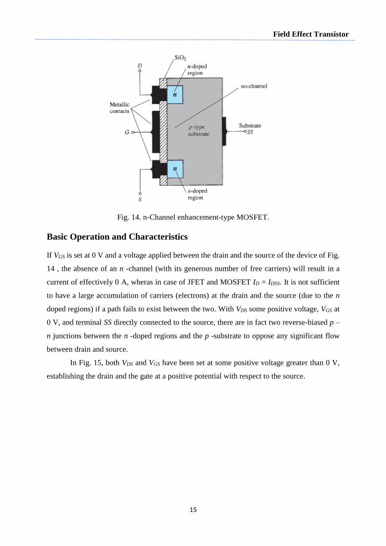
Basic Construction The basic construction of the n -channel enhancement-type MOSFET is provided in Fig. 14 .
A slab of p -type material is formed from a silicon base and is again referred to as the substrate.
As with the depletion-type MOSFET, the substrate is sometimes internally connected to the
source terminal, whereas in other cases a fourth lead (labeled SS) is made available for external
control of its potential level. The source and drain terminals are again connected through
metallic contacts to n -doped regions, but in Fig. 6.32 the absence of a channel between the two
n -doped regions. This is the primary difference between the construction of depletion-type and
enhancement-type MOSFETs—the absence of a channel as a constructed component of the
device. The SiO2 layer is still present to isolate the gate metallic platform from the region
between the drain and source, but now it is simply separated from a section of the p-type
material. Therefore, we can say that the construction of an enhancement-type MOSFET is quite
similar to that of the depletion-type MOSFET, except for the absence of a channel between the
drain and source terminals.
15
Field Effect Transistor
Fig. 14. n-Channel enhancement-type MOSFET.
Basic Operation and Characteristics If VGS is set at 0 V and a voltage applied between the drain and the source of the device of Fig.
14 , the absence of an n -channel (with its generous number of free carriers) will result in a
current of effectively 0 A, wheras in case of JFET and MOSFET ID = IDSS. It is not sufficient
to have a large accumulation of carriers (electrons) at the drain and the source (due to the n
doped regions) if a path fails to exist between the two. With VDS some positive voltage, VGS at
0 V, and terminal SS directly connected to the source, there are in fact two reverse-biased p –
n junctions between the n -doped regions and the p -substrate to oppose any significant flow
between drain and source.
In Fig. 15, both VDS and VGS have been set at some positive voltage greater than 0 V,
establishing the drain and the gate at a positive potential with respect to the source.

16
Field Effect Transistor
Fig. 15. Channel formation in the n-channel enhancement-type MOSFET.
The positive potential at the gate will pressure the holes (since like charges repel) in the p -
substrate along the edge of the SiO2 layer to leave the area and enter deeper regions of the p -
substrate, as shown in the figure. The result is a depletion region near the SiO2 insulating layer
void of holes. However, the electrons in the p-substrate (the minority carriers of the material)
will be attracted to the positive gate and accumulate in the region near the surface of the SiO2
layer. The SiO2 layer and its insulating qualities will prevent the negative carriers from being
absorbed at the gate terminal. As VGS increases in magnitude, the concentration of electrons
near the SiO2 surface increases until eventually the induced n-type region can support a
measurable flow between drain and source. The level of VGS that results in the significant
increase in drain current is called the threshold voltage and is given the symbol VT . On
specification sheets it is referred to as VGS(Th), although VT is less unwieldy and will be used in
the analysis to follow. Since the channel is nonexistent with VGS =0 V and “enhanced” by the
application of a positive gate-to-source voltage, this type of MOSFET is called an
enhancement-type MOSFET. Both depletion- and enhancement-type MOSFETs have

17
Field Effect Transistor
enhancement-type regions, but the label was applied to the latter since it is its only mode of
operation.
As VGS is increased beyond the threshold level, the density of free carriers in the induced
channel will increase, resulting in an increased level of drain current. However, if we hold VGS
constant and increase the level of VDS , the drain current will eventually reach a saturation level
as occurred for the JFET and depletion-type MOSFET. The leveling off of ID is due to a
pinching-off process depicted by the narrower channel at the drain end of the induced channel
as shown in Fig. 16.
Fig.16. Change in channel and depletion region with increasing level of VDS for a fixed value
of VGS.
Applying Kirchhoff’s voltage law to the terminal voltages of the MOSFET of Fig. 16., we find
that
DG DS GSV V V (1)
If VGS is held fixed at some value such as 8 V and VDS is increased from 2 V to 5 V, the voltage
VDG (by Eq.(1)) will increase from –6 V to –3 V and the gate will become less and less positive
with respect to the drain. This reduction in gate-to-drain voltage will in turn reduce the
attractive forces for free carriers (electrons) in this region of the induced channel, causing a
reduction in the effective channel width. Eventually, the channel will be reduced to the point

18
Field Effect Transistor
of pinch-off and a saturation condition will be established as happen in the JFET and depletion-
type MOSFET. In other words, any further increase in VDS at the fixed value of VGS will not
affect the saturation level of ID until breakdown conditions are encountered.
The drain characteristics of Fig. 17 reveal that for the device of Fig. 14 with VGS = 8 V,
saturation occurs at a level of VDS = 6 V. In fact, the saturation level for VDS is related to the
level of applied VGS by
satDS GS TV V V (2)
Obviously, therefore, for a fixed value of VT , the higher the level of VGS , the greater is the
saturation level for VDS , as shown in Fig. 14 by the locus of saturation levels.
Fig. 17. Drain characteristics of an n-channel enhancement-type MOSFET with VT =2V and 3 20.278 10k A V
For values of V GS less than the threshold level, the drain current of an enhancement-type
MOSFET is 0 mA.
Figure 17 clearly reveals that as the level of VGS increases from VT to 8 V, the resulting
saturation level for ID also increases from a level of 0 mA to 10 mA. In addition, it is quite
noticeable that the spacing between the levels of VGS increases as the magnitude of VGS
increases, resulting in ever-increasing increments in drain current. For levels of VGS >VT, the
drain current is related to the applied gate-to-source voltage by the following nonlinear
relationship:

19
Field Effect Transistor
2
D GS TI k V V (3)
The equation (3) shows a nonlinear (curved) relationship between ID and VGS . The k term is a
constant that is a function of the construction of the device. The value of k can be determined
from the equation (4),where onDI and VGS(on) are the values for each at a particular point on the
characteristics of the device.
2
( )
onD
GS on T
Ik
V V
(4)
Fig. 18. Sketching the transfer characteristics for an n- channel enhancement-type MOSFET
from the drain characteristics.