sub-micron indium pillar fabrications
TRANSCRIPT
Sub-Micron Indium
Pillar
Fabrications
by
Pantea Pervissian
A thesis
presented to the University of Waterloo
in fulfillment of the
thesis requirement for the degree of
Master of Applied Science
in
Chemical Engineering
Waterloo, Ontario, Canada, 2009
© Pantea Pervissian 2009

ii
Author’s Declaration
I hereby declare that I am the sole author of this thesis. This is a true copy of the thesis, including
any required final revisions, as accepted by my examiners.
I understand that my thesis may be made electronically available to the public.
Pantea Pervissian

iii
Abstract
The laws of classical mechanics show that mechanical properties are independent of
sample sizes. However, based on extensive theoretical work and experimentation, it is believed
that reducing the size of materials to the submicron scale can result in different mechanical
properties than those found in bulk quantities. This size effect was explained by the strain
gradient. Atomic simulations have shown that yield stress depends on size even in the absence of
the strain gradient. All of the experiments done on material creep behaviour, reported in the
literature, have been conducted in the presence of strain gradient.
This thesis focuses on the fabrication methods of freestanding indium pillar samples
created by two unique methods; focused ion beam (FIB) and the micro-fabrication approach. The
low melting point indium metal limits the application of FIB to form the sub-micron pillars. As a
result, two different micro-lithography techniques, ultra-violet radiation and electron-beam
lithography, were developed to fabricate these nano-pillars. In order to monitor the creep
mechanism, which was dominant in this testing, the samples were then divided into two groups:
polycrystalline and single-crystal pillars, each in different sizes. These pillars will later be
compressed by a nano-indenter using a flat punch. Compressive stress, strain, and stiffness of the
pillars will be measured to verify if the indium mechanical behavior deviates from the bulk in the
absence of strong strain gradient.

iv
Acknowledgements
I would like to express my sincere gratitude to my supervisor, Dr. Ting Y. Tsui, for the
opportunity that he has given me and for his guidance, inspiration, and insight throughout this
work and my studies.
I would also like to thank Arash Tajik for his invaluable suggestions throughout this work
and also Gyuhyon Lee for his endless help through the experiments. I am just as grateful to Dr.
Todd Simpson of the Nanofabrication Laboratory of the University of Western Ontario. His
knowledge and insight in this work is appreciable.
Special thanks are due to Dr. Mark Pritzker for lending us his lab to perform our
experiments and also to Jorge Vazquez for his patience during our time in the lab.
Above all, I am grateful to my parents and my sister for their endless love and continuous
support in every single moment of my life.

v
Table of Contents
List of Tables………………………………………………………………………………………...viii
List of Figures………………………………………………………………………………………....ix
List of Symbols ………………………………………………………………………………………xii
List of Glossary……………………………………………………………………………………….xv
Chapter 1 Introduction ........................................................................................................................... 1
1.1 Theory .......................................................................................................................................... 1
1.1.1 Material Strength................................................................................................................... 1
1.1.2 Elastic-Plastic Behaviour ...................................................................................................... 1
1.1.3 Average Stress–Strain ........................................................................................................... 2
1.1.4 Types of Stress-Strain ........................................................................................................... 3
1.1.5 Tensile Deformation in Ductile Metals ................................................................................. 3
1.1.6 Mechanical Failure ................................................................................................................ 5
1.1.6.1 Excessive Elastic Deformation ...................................................................................... 5
1.1.6.2 Yielding .......................................................................................................................... 5
1.1.6.3 Fracture .......................................................................................................................... 5
1.1.7 Plastic Deformation of Single Crystals ................................................................................. 6
1.1.8 Crystal Geometry Concepts .................................................................................................. 6
1.1.9 Lattice Defect ........................................................................................................................ 9
1.1.9.1 Point Defect ................................................................................................................... 9
1.1.9.2 Dislocation ..................................................................................................................... 9
1.1.9.2.1 Burger Vector ........................................................................................................ 10
1.1.9.2.2 Dislocation Line .................................................................................................... 10
1.1.9.2.3 Edge Dislocation ................................................................................................... 10
1.1.9.2.4 Screw Dislocation ................................................................................................. 11
1.1.10 Creep ................................................................................................................................. 11
1.1.10.1 Creep Curve ............................................................................................................... 12
1.1.10.2 Types of Creep ........................................................................................................... 13
1.1.10.2.1 Nabarro-Herring Creep ....................................................................................... 14
1.1.10.2.2 Coble Creep......................................................................................................... 14

vi
1.1.10.2.3 Creep Activation Energy ..................................................................................... 14
1.2 Motivation of Size-Dependent Creep Behaviour of Materials................................................... 16
1.2.1 Indium Creep Behaviour ..................................................................................................... 18
1.2.2 Indium ................................................................................................................................. 18
1.2.3 Indentation Size Effect ........................................................................................................ 21
1.3 Objective of the Work ................................................................................................................ 22
Chapter 2 Sample Design ..................................................................................................................... 23
2.1 Introduction ................................................................................................................................ 23
2.2 Sample Design ........................................................................................................................... 23
2.3 Fabrication Techniques .............................................................................................................. 25
2.3.1 Focus Ion Beam Instrument ................................................................................................ 26
2.3.1.1 The Stage ..................................................................................................................... 28
2.3.1.2 Imaging Detector.......................................................................................................... 29
2.3.1.3 Gas Injectors ................................................................................................................ 29
2.3.2 Microlithography ................................................................................................................ 30
2.3.2.1 Micro- Mold Fabrication .............................................................................................. 31
2.3.2.1.1 Micro-Mold Chips Design .................................................................................... 31
2.3.2.1.2 Micro-Mold Fabrication Process........................................................................... 33
2.3.2.2 Electro-Depositing ....................................................................................................... 34
2.3.2.2.1 Principal of Electroplating Process ....................................................................... 35
2.3.2.2.2 Current Density ..................................................................................................... 36
2.3.2.3 Revealing the Pillars .................................................................................................... 37
Chapter 3 Sample Fabrication .............................................................................................................. 39
3.1 Introduction ................................................................................................................................ 39
3.2 Sample Fabrication .................................................................................................................... 39
3.2.1 Sample Fabrication using the Focused Ion Beam (FIB) ..................................................... 40
3.2.2 Focus Ion Beam Fabrication Results................................................................................... 41
3.2.3 Sample Fabrication using Microlithography ....................................................................... 45
3.2.3.1 Substrate ....................................................................................................................... 45
3.2.3.2 Gold & Chromium Deposition ..................................................................................... 46
3.2.3.2.1 E-beam Evaporation Deposition ........................................................................... 47

vii
3.2.3.3 Types of Microlithography .......................................................................................... 49
3.2.3.3.1 Ultraviolet Lithography ......................................................................................... 50
3.2.3.3.1.1 Spin Coating SU-8 ......................................................................................... 52
3.2.3.3.1.2 SU-8 Soft Bake .............................................................................................. 53
3.2.3.3.1.3 Chromium Photo Mask .................................................................................. 53
3.2.3.3.1.4 Ultraviolet Exposure on SU-8 Resist ............................................................. 56
3.2.3.3.1.5 SU-8 Post-exposure Baking ........................................................................... 57
3.2.3.3.1.6 Developing SU-8 ............................................................................................ 58
3.2.3.3.2 E-beam Lithography ............................................................................................. 60
3.2.3.3.2.1 Emulsion Photo Mask .................................................................................... 63
3.2.3.3.2.2 Coating Gold Chips AZ Photo Resist ............................................................ 67
3.2.3.3.2.3 Oxygen Plasma Etch ...................................................................................... 70
3.2.3.3.2.4 PMMA Photo Resist Coating ......................................................................... 70
3.2.3.3.2.5 E-Beam Writing on PMMA ........................................................................... 71
3.2.3.3.2.6 Developing PMMA ........................................................................................ 72
3.2.3.3.2.7 Oxygen Plasma Etching ................................................................................. 75
3.2.3.4 Electroplating ............................................................................................................... 77
3.2.3.5 Stripping Photo Resist .................................................................................................. 79
3.3 Some of the Fabricated Pillars ................................................................................................... 81
Chapter 4 Result of Micro-Lithography Fabrication ........................................................................... 85
4.1 Introduction ................................................................................................................................ 85
4.2 Effect of Ultraviolet Dosage ...................................................................................................... 85
4.3 Effect of Air Gap between the Photo Mask and Photo Resist ................................................. 90
4.4 Pulse Plating............................................................................................................................... 96
4.5 Oxygen Plasma Etch ................................................................................................................ 101
Chapter 5 Summary ........................................................................................................................... 104
5.1 Recommendations .................................................................................................................... 105
REFERENCES……………………………………………………………………………….106
APPENDIX A: Best Known Method for Fabricating 0.25μm Pillars………………………………115

viii
List of Tables
Table 1.1 Atomic density (No. atoms/
A3), crystallographic directions in indium, reproduced from [53] 19
Table 1.2. Atomic density (No. atoms/
A3), crystallographic directions in indium, reproduced from [53] 20
Table 3.1 Milling condition of 10 μm pillar with FIB ................................................................................ 42
Table 3.2 Milling condition for 3 μm with FIB .......................................................................................... 43
Table 3.3 Cr/Au deposition conditions ....................................................................................................... 48
Table 3.4 Supplementary conditions for Cr/Au deposition ........................................................................ 49
Table 3.5 Omni coat spin coating conditions .............................................................................................. 51
Table 3.6 SU-8 Spin coating conditions ..................................................................................................... 52
Table 3.7 SU-8 soft bake Conditions .......................................................................................................... 53
Table 3.8 SU-8 post exposure bake conditions ........................................................................................... 57
Table 3.9 Plating condition for the UV-10μm micro-mold ....................................................................... 81
Table 3.10 Plating condition of the E-Beam-500nm micro-mold .............................................................. 82
Table 3.11 Plating condition for E-Beam-250nm micro-mold ................................................................... 83
Table 3.12 Plating condition for E-beam-250 micro-mold ......................................................................... 84
Table 4.1 PMMA etching rates corresponding to the applied .................................................................. 102
Table 5.1 Oxygen etch condition for removing AZ residues .................................................................... 118
Table 5.2 Oxygen Etch condition for removing PMMA residues ............................................................ 120

ix
List of Figures
Figure 1.1 Tension stress-strain curve .......................................................................................................... 4
Figure 1.2 Simple cubic structure ................................................................................................................. 7
Figure 1.3 (a) Body-Centered cubic structure (b) Face-Centered cubic structure ........................................ 8
Figure 2.1 Schematic of sample overall design .......................................................................................... 24
Figure 2.2 Summery of sample design........................................................................................................ 25
Figure 2.3 Basic Focus Ion Beam instrument, reproduced from [54] ......................................................... 27
Figure 2.4 General steps in fabrication of pillars via microlithography: (1) micro- mold fabrication (2)
indium deposition (3) revealing the pillars ................................................................................................. 30
Figure 2.5 (a) Overall view of the Micro Mold chip (b) SEM image of the controlling surface side wall (c)
SEM image of the patterned area side wall ................................................................................................. 32
Figure 2.6 Steps for fabrication of micro-mold ......................................................................................... 34
Figure 2.7 Schematic of plating bath .......................................................................................................... 35
Figure 2.8 SEM image of fabricated pillars via micro lithography ............................................................ 38
Figure 3.1 I-Beam image of 10 μm pillars. Crater size is 30 μm. Current was 2000 pA, and dosage was
500 μC /cm² ................................................................................................................................................ 42
Figure 3.2 Top view I-beam image of 30μm crater and 5 μm island .......................................................... 43
Figure 3.3 I-beam image of FIB fabricated pillar having a diameter of 2.85 μm ....................................... 44
Figure 3.4 Schematic over view design of chromium mask fabricated at University of Alberta ............... 54
Figure 3.5 (a) Schematic of 0.5 μm photo mask on chromium mask (b) batch of 0.5 μm circular pattern
(c) controlling surface pattern ..................................................................................................................... 55
Figure 3.6 SEM image of a SU-8 holes side wall, developed for less than 6 min ...................................... 58
Figure 3.7 SEM image a SU-8 holes side wall, developed for 6 min ......................................................... 58
Figure 3.8 (a-b) SEM image of controlling surface side wall on a UV-micro-mold chip .......................... 59
Figure 3.9 (a-b) SEM image of holes side wall on a UV Micro–mold chip ............................................... 60
Figure 3.10 (a-e) Steps for patterning the controlling area using an emulsion mask a) blank gold chip b)
AZ-photo resist coating c) patterning controlling area d) gold and chrome etch e) striping the resist to
reveal the gold surface for the next step. .................................................................................................... 62
Figure 3.11 Schematic steps in fabrication of pillar growth site: a) tapping the controlling surface, b) spin
coating PMMA, c) writing the patterned area with E-beam ....................................................................... 63

x
Figure 3.12 Schematic of emulsion mask ................................................................................................... 64
Figure 3.13 Schematic of mylar design ...................................................................................................... 65
Figure 3.14 Schematic of categorized area using the UV lithography........................................................ 68
Figure 3.15 Schematic design of the pillar growth site ............................................................................... 71
Figure 3.16 E-Beam write map with the applied dosage in each location. ................................................. 72
Figure 3.17 Schematic of overall design of the E-beam micro – mold chip ............................................... 73
Figure 3.18 (a-b) SEM image of processed E-Beam micro-mold chip: (a) Pillar growing site (b)
controlling surface ...................................................................................................................................... 74
Figure 3.19 Schematic of the side wall mold design .................................................................................. 74
Figure 3.20 Schematic of DC circuit .......................................................................................................... 77
Figure 3.21 SEM image of one of the pillar site batches in E- beam micro-mold chip samples ................ 79
Figure 3.22 SEM images of 10μm pillars ................................................................................................... 81
Figure 3.23 SEM image of plated pillar diameter 0.5 μm height of 1.5 μm ............................................... 82
Figure 3.24 SEM image of the 0.5 μm plated indium. [10min deposition time was high so the over
plating indium forms these mushrooms ...................................................................................................... 82
Figure 3.25 SEM image of 250 nm indium pillar ....................................................................................... 83
Figure 3.26 SEM images of 250nm fabricated pillars ................................................................................ 84
Figure 4.1 Different film thicknesses of SU-8 absorbance vs. UV wavelength, reproduced from [65] ..... 86
Figure 4.2 ((a)-(d)) SEM image of fabricated mold (a) – (b) dosage 1000 mJ/cm2, (c)-(d) dosage 1800 mJ
/cm2 ............................................................................................................................................................. 87
Figure 4.3 SEM image of the side wall as well as the holes on the micro-mold chip according to the
applied condition ......................................................................................................................................... 88
Figure 4.4 SEM image of the side wall as well as the holes on the micro-mold chip according to the
applied condition ......................................................................................................................................... 89
Figure 4.5 SEM image of the side wall as well as the holes on the micro-mold chip according to the
applied condition ......................................................................................................................................... 89
Figure 4.6 SEM image of developed 10 μm chip after post exposure bake................................................ 90
Figure 4.7 Schematic illustration of UV-light deviation due to the air gap ................................................ 91
Figure 4.8 Schematic illustration of photo resist exposed and unexposed area under photo-mask black
patterns ........................................................................................................................................................ 92

xi
Figure 4.9 Intensity distribution of Fresnel diffraction for different air gap thickness: L fx Fresnel
diffraction intensity, L inc intensity of incident vs. the photo mask distance from photo resist surface,
reproduced from [69] .................................................................................................................................. 93
Figure 4.10 Intensity distribution of Fresnel diffraction before and after injecting Glycerol: L fx Fresnel
diffraction intensity, L inc intensity of incident vs. the photo mask distance from photo resist surface,
reproduced from [69] .................................................................................................................................. 94
Figure 4.11 SEM image of developed micro-mold side wall after Glycerol inject .................................... 94
Figure 4.12 SEM image of micro-mold side wall corresponding to the applied condition, before Glycerol
inject ............................................................................................................................................................ 95
Figure 4.13 SEM image of micro-mold side wall corresponding to the applied condition, after Glycerol
inject ............................................................................................................................................................ 95
Figure 4.14 Applied pulse plating wave form current density vs. time ...................................................... 97
Figure 4.15 Favored wave form for plating the micro-mold chips using potentiostat current density vs.
time ............................................................................................................................................................. 98
Figure 4.16 SEM image of plated 250 nm micro-mold chip using potentiostat by applying 0.2 second 10.4
mA /cm² and 10 min of 1.04 mA/ cm² current density. ............................................................................. 99
Figure 4.17 The applied wave form using Dc Power supply, current density mA /mm² vs. time(s). ....... 100
Figure 4.18 SEM images of 250 nm pillars using Dc Power supply with 3.5 second 10.4 mA/cm² current
density and 10 min of 1.04 mA/cm² current density. ................................................................................ 101
Figure 4.19 SEM images of 250 nm pillars using Dc Power supply with 3.5 second 10.4 mA/cm² current
density and 10 min of 1.04 mA /cm² current density and oxygen plasma etch ........................................ 103
Figure 5.1 E-Beam write map with the applied dosage in each section.................................................... 119

xii
List of Symbols
.
Creep rate
Angle change
A Current
a Distance between the planes
A Area
b Creep mechanism exponent
C Constant depending on the material
D Grain size
E Young’s module
F Faraday constant
h Height
H Hardness
i Current density
k Boltzmann’s constant
L Length
L1 Initial length

xiii
Lfx Fresnel diffraction intensity
Linc Intensity of incident
m Transferred mass from the anode to cathode
M Molecular weight
m Creep mechanism exponent
n Number of transferred electrons
P Load
Q Creep activation energy
R Gas constant
t Time period
T Temperature
V Voltage
γ Shear strain
δ Length change
ε Average strain
η Efficiency
ρ Density

xiv
ζ Average stress
η Shear stress

xv
List of Glossary
Climb: Motion of dislocation to the slip plane
Cross Slipping: transfer of glide of a screw dislocation from one slip plane to another during
deformation or thermal recovery.
Dielectric Constant: degree of polarization or charge storage capability of a material when
subjected to an electric field.
Dislocation Line: the intersection of the extra half-plane of atoms with the slip plane.
Dislocation Starvation: a state at which the crystal structure is free of dislocations
Dislocation: a linier crystalline defect.
Elastic Limit: stress at which the material starts to behave in a non-elastic manner.
Eucentric Position: eucentric implies, in specimen stage, that tilting the specimen can be
achieved without the field of view moving. This is a highly desirable attribute of a
microscope stage.
Failure: when a material loses its ability to satisfy the original design function.
Fresnel Diffraction: a process of diffraction which occurs when a wave passes through an
aperture and diffracts in the near field.
Glide: motion of dislocations on the slip plane
xvi
Grain Boundary: zone formed at the junction of individual crystals in a polycrystalline
material.
Hardness: resistance of materials surface to abrasion, scratching and indentation.
Jog: a step of atomic dimensions in a dislocation line. The Jog that lays in the glide plane of
the dislocation known as a kink. Jogs may be formed by thermal activation at high
temperatures and may also be formed at low temperatures by the intersection of dislocations.
Lattice: a lattice is the set of points upon which a crystal may be built by placing an identical
basis, in the same orientation, on each of the lattice points.
Melting Point: temperature at which a material turns suddenly from solid to liquid.
Microstructure: the structural features of an alloy that is subject to observation under a
microscope.
Necking: reducing the cross sectional area of the metal in an area by stretching.
Notches: V-shaped cut.
Perfect Crystal: crystal contains no defect.
Pinning: dislocations may get pin at points along their length by various objects including
particles, grain boundaries and intersecting dislocations. Once pinned, a dislocation cannot
glide.
Poisson’s Ratio: negative ratio of the thickness decrease divided by the length increase as a
result of a tensile stress applied to a material.

xvii
RCA Clean: standard wafer cleaning steps.
Real Crystal: crystal contains no defect.
Resistivity: intrinsic materials property that describes the ability of a material to resist, or
oppose, the transport of electrical charge in response to an external electric field
Shear Modulus: ratio of shear stress divided by the shear strain in the elastic region. It can
also be referred to as modulus of rigidity or torsion modulus.
Slip Displacement: the process which allows plastic flow to occur in metals, where the
crystal planes slide past one another.
Slip Line: one part of the crystal slide as a unit across the neighboring side part along the slip
direction on the surface of the plane, the line intersection of this surface with the outer
surface of the crystal is called slip line.
Taylor Cone: cone observed in electro spinning and electro spraying process
Tensile Strength: maximum tensile stress a material can withstand before failure.
Thermal Expansion: term used to describe the change in dimensions that occurs with most
materials as the temperature is increased or decreased
Un slipped Area: area where no planed have been slipped.
Young's Modulus: the proportionality constant of solids between elastic stress and elastic
strain and describes the inherent stiffness of a material.

1
Chapter 1
Introduction
1.1 Theory
1.1.1 Material Strength
Material strength is expressed as the relationship between the internal forces, external
load, and deformation in the material. The internal forces are defined as the stress acting over a
certain area and are equal to the integral of the stress multiplied by the differential area upon
which the stress acts. Since stress distribution cannot be physically measured, it can be
substituted by strain distribution because these two qualities are proportional to each other.
1.1.2 Elastic-Plastic Behaviour
All solid materials deform when subjected to external loads. When the applied load is
small, a solid will recover to its original shape after the load is removed. This behaviour is called
elastic deformation and the limit beyond which the material no longer behaves elastically is
called the elastic limit. If the load exceeds the elastic limit of a material, the deformation will be
permanent. This permanent deformation is also known as plastic deformation. For most
materials, deformation is linearly proportional to the load within the elastic limit. This
relationship is expressed by Hook’s Law but and is more commonly referred to as the stress-
strain relationship [1].

2
1.1.3 Average Stress–Strain
As an example of how average stress-strain is expressed, consider a uniform cylindrical
bar of a certain gage length (L1) subjected to an axial tensile load. The average strain (ε) is the
ratio of the changes in the bar length relative to its initial length.
ε 1
1
1 L
LL
L
1-1
Strain is dimensionless since both L and δ are measured in unite of length. The load (P) being
applied to the bar is balanced by the internal resisting force ( Ad ):
P= Ad 1-2
Where P is the load, ζ is the stress and A is the area upon which the stress is acting. Although the
stress is not uniformly distributed over the surface, the average stress is defined as:
A
P
1-3
Hook’s Law can then represent the strain and stress relationship as follows:
E 1-4
E is known as the module of elasticity, or Young’s module.

3
1.1.4 Types of Stress-Strain
The stress acting upon a surface can be divided into two components: the nominal stress
(ζ) which is perpendicular to the surface and shear stress ( ) which is parallel to the surface:
sin
cos
A
P
A
P
1-5
Therefore, shear stress and normal stress can be defined for any plane. The strain can be divided
in two elements for the acting force: the natural strain (ε) and the shear strain ( ). Natural strain
is defined as the change in a linear dimension divided by the instantaneous value of the
dimension.
1
ln
1L
L
L
dLL
L
1-6
Shear strain is the angle of rotation. If the angular change is assumed to be , the displacement
due to shear stress must be equal to a and the distance between the planes be h, The shear strain
will then be the ratio of a/h or the tangent of angle change :
tanh
a 1-7
1.1.5 Tensile Deformation in Ductile Metals
In tension tests, specimens are subjected to an increasing load until they fracture. This
process allows the basic mechanical property of materials to be determined. Load and elongation

4
are measured at frequent intervals during the test. The average stress and the average strain are
plotted in a stress-strain diagram.
Str
ess σ
Strain e
s Y
k
σm
ax
fra
ctu
re
0
Fig.1 Tension stress-strain curve (reproduced from[1])
Figure 1.1 Tension stress-strain curve
The curve OS in Figure 1.1 is the elastic region in which Hook’s Law is obeyed. Point S is the
elastic limit. The slope of this curve gives the elastic module E. Point Y is the yield stress which
will produce a small amount of permanent deformation. The permanent strain (O-k)
corresponding to this stress is about 0.01-0.02 percent of the initial length. At the stress beyond
the yield point, plastic deformation increases and metals become stronger so that the load
required for deforming the specimen increases. The flow stress will reach a maximum value and

5
is called the ultimate tensile strength. The diameter of the specimen will decrease from this point
while the stress required for further deformation will decrease until the specimen fractures.
1.1.6 Mechanical Failure
Mechanical failures may be categorized into three areas: (1) excessive elastic deformation, (2)
yielding, and (3) fracture.
1.1.6.1 Excessive Elastic Deformation
Materials can experience excessive elastic deformation under conditions of equilibrium
when a load is gradually applied, or under the conditions of unstable equilibrium. Excessive
elastic deformation can result in fracture for brittle materials such as glass.
1.1.6.2 Yielding
Yielding is a permanent deformation at which point the elastic limit is exceeded. Due to
strain-hardening at room temperature or under constant loading, yielding rarely results in
fracture. Metals deforms continually under a constant stress at higher temperatures, and do not
show a strain hardening. This time-dependent yielding is called creep. Failure prediction is
complicated by the fact that a mechanical property of a material can change during loading, and
also that stress at this point is not proportional to strain.
1.1.6.3 Fracture
Fracture can occur in three general ways: (1) brittle fracture, (2) fatigue, (3) delayed
fracture.

6
(1) Fracture will occur in brittle materials when the applied stress is greater than their
elastic limit. Decreases in temperature, increases in load rate, or the presence of notches may
cause ductile metals to experience brittle fracture.
(2) Fatigue occurs in metals when the applied load is smaller than the yield stress and the
applied load fluctuates or is alternating. Minute cracks will progress gradually until catastrophic
failure.
(3) Delayed fracture will occur when a constant load is applied to a part for a long period
of time. Fracture can occur without any significant sign of yielding, depending upon the
temperature and the stress that is being applied.
1.1.7 Plastic Deformation of Single Crystals
Many experiments have been conducted on metallic crystals since the discovery of X-
rays, to reveal the relationship between plastic behaviour and the atomic structure of metals. To
investigate this relationship in the absence of the effect of the grain boundaries and neighboring
grain boundaries, most of these studies have been carried out on single-crystal specimens.
1.1.8 Crystal Geometry Concepts
The atoms in metal crystals have a regular, repeated three-dimensional pattern. This
arrangement appears as a crystal lattice in which the atoms are placed in a particular location.
The crystallographic plane and direction are used to address the atoms in the crystals more
easily. For example, the atoms in a simple cubic lattice crystal structure are located at the edge of
the cubic lattice, as illustrated in Figure 1.2.

7
:
A
B
D
C
E
F
G
H
Z
X
y
Fig 2. Simple cubic structure
Figure 1.2 Simple cubic structure
After specifying the three axes (x, y, and z) through one corner of the crystal, the
crystallographic plane and directions can be defined with respect to these axes. The plane BCDE
in Figure 1.2 is parallel to the y and z axes and intersects with the x axis, so it will be designed as
(100). There are six crystallographic planes to a cubic crystal: (010), (001), (100), (100), (010),
and (001). The bar indicates the plane’s interaction with the axes in the negative direction.
Crystallographic direction (110) represents the direction of HD, as this direction is obtained by
moving from H to C and from C to D.
Many metal crystals have either a body-centered cubic (BCC) structure or a face-centered
structure (FCC). As shown in Figure 1.3, the body-centered cubic structure has one atom in the

8
body of the crystal, and 8 atoms in each corner. Each atom is surrounded by eight atoms, so the
number of atoms per crystal structure will be two: (8/8+1) = 2. In face-centered crystals, there is
an atom in the center of each cubic face in addition to the corner atoms, making four atoms per
structure. This is because the atoms in the center of the cubic face belong to two units: (8/8+6/2)
= 4. In order to modify the planes and directions in the hexagonal close-packed structure (HCP),
four axes should be used. Plastic deformation in this case is mainly limited to low-index planes
that have a higher atom density.
:
A
B
D
C
E
F
G
H
Z
X
y
Fig 3. a) body center cubic structure b) face center cubic structure
:
A
B
D
C
E
F
G
H
Z
X
y
(a)(b)
Figure 1.3 (a) Body-Centered cubic structure (b) Face-Centered cubic structure
9
1.1.9 Lattice Defect
As is to be expected, the arrangement of real crystals is imperfect. Instead, their
structures deviate from perfect crystals due to the presence of some defects. Studying lattice
defects is crucial because they directly affect the mechanical behaviour of materials. Any
deviation from the ordinary crystal structure is called a defect. When this deviation is related to
only a few atoms it is called a point defect. However, when defects increase they can be divided
into three different categories: line, surface, and plane defects.
1.1.9.1 Point Defect
There are three types of point defects:
I. Vacancy defects occur when an atom is missing from the normal lattice; these can be
created by thermal excitation. Bombardment by high-energy particles can also result in
increasing vacancy concentration [1]. If the density of vacancies increases they will
cluster together and voids may be formed.
II. Interstitial defects are the results of an atom being trapped inside the normal lattice. This
type of point defect is the result of bombardment with high-energy particles rather than
thermal activation.
III. The presence of impurities at the interstitial positions or in the lattice positions is another
type of point defect.
1.1.9.2 Dislocation
The most important line defects are dislocations, which are responsible for the slip
phenomenon. Dislocations can also be defined by the line that separates the slipped and
10
unslipped areas in the crystals. Dislocations can move through the crystal in the absence of
obstacles in response to the applied load, and the slips occur in the area over which they move.
This can explain why real crystals deform much more easily compared to perfect crystals. The
existence of dislocations can also clarify plastic deformation (strain hardening). Understanding
dislocation is important not only for explaining the slip of crystals but also for studying all
mechanical behaviour.
1.1.9.2.1 Burger Vector
The Burger vector is a vector whose magnitude is equal to the magnitude of the slip
displacement and its direction, thus giving the direction of the slip. It can also be defined by the
Burger circuit, which is a circuit that starts at one atomic position and traverses the same number
of atoms on each side of the lattice until it reaches the starting point once again. If the circuit
fails to close itself, the closure defect is called the Burger vector.
1.1.9.2.2 Dislocation Line
The plane that contains the dislocation is called the slip plane, and the dislocation line is
the line that separates the slipped from the unslipped region. It never ends in the crystal unless it
reaches the surface, forms a loop, or joins the other dislocation lines.
1.1.9.2.3 Edge Dislocation
Edge dislocation is one of two types of dislocations. This defect is usually a half-plane of
atoms inserted into a portion of crystal as a response to an applied stress; thus, the Burger vector
will be perpendicular to the dislocation line for edge dislocation. The climb of the edge

11
dislocation can occur due to the existence of vacancies. The vacancies change the atomic
position so that the dislocation will climb the dislocation line and a jog will form at that point.
Applying stress in a certain direction which is not in the direction of jog dislocations will pine
the dislocation at the jog locations and the stress will bow them out in the form of loops. These
loops can no longer be characterized as the edge dislocation and are called either screw or mix
dislocations.
1.1.9.2.4 Screw Dislocation
The slip in the screw dislocation occurs while the top and bottom of the crystals are being
subjected to shear stress. The upper half of the crystal is displaced with respect to the bottom half
in a helical motion. The Burger vector and dislocation line are parallel. The slip plane is different
in every type of the crystals. For example, in face-centered cubic metals the slip occurs on the
111 planes since their vertical separation distance is great and they are also the densest planes.
The slip direction is <110> type direction. Screw dislocation can overcome this obstacle in
crystals by cross slipping.
In reality, crystal dislocations are not straight lines and do not lie in a single crystal
plane. However the character of most of the dislocations is formed partly of edge dislocations
and partly of screw dislocations, which is called the mix dislocation [2].
1.1.10 Creep
Creep is defined as a plastic deformation that occurs under a constant load at high
temperature during a long period of time. Industry seems to be having difficulty successfully
using metals at elevated temperatures because the strength of metal decreases as temperature

12
increases. The deformation mechanisms of metals change at high temperature and have a strong
effect on the dislocation mobility, equilibrium concentration of vacancies, slip systems, grain
boundary deformation, as well as other important factors [2]. Thus, it is important to investigate
the mechanical properties of materials at elevated temperatures.
The duration that materials bear stress also plays an important role in determining their
strength at the high temperatures. The creep test measures the dimensional change of material
with respect to time. Some other high-temperature tests such as stress-rupture, relaxation, and
thermal-shock resistance tests can be used to measure some other special properties of materials
[2].
1.1.10.1 Creep Curve
Applying a constant stress greater than the elastic limit, materials show three stages of
creep deformation, as illustrated in the creep curve in Figure 1.4. The primary stage of the creep,
in which the strain rate decreases, can be the result of the dislocation climb, thermally-activated
atom mobility, or additional slip plane, all of which enhance the deformation mechanism. The
secondary stage, in which the strain rate is constant, can result from the balance between the
increment of the slip plane and the increment of resistance to this increment due to the buildup of
dislocations and other micro-structural barriers. In the final stage, the strain rate increases due to
necking or internal cracking.
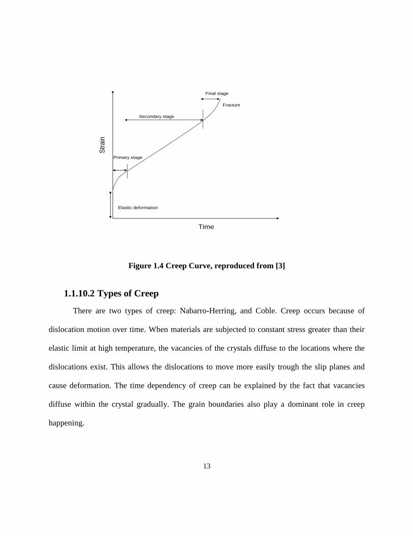
13
Elastic deformation
Time
Str
ain
Primary stage
Secondary stage
Final stage
Fracture
Figure 1.4 Creep Curve, reproduced from [3]
1.1.10.2 Types of Creep
There are two types of creep: Nabarro-Herring, and Coble. Creep occurs because of
dislocation motion over time. When materials are subjected to constant stress greater than their
elastic limit at high temperature, the vacancies of the crystals diffuse to the locations where the
dislocations exist. This allows the dislocations to move more easily trough the slip planes and
cause deformation. The time dependency of creep can be explained by the fact that vacancies
diffuse within the crystal gradually. The grain boundaries also play a dominant role in creep
happening.

14
1.1.10.2.1 Nabarro-Herring Creep
In Nabarro-Herring creep, atoms diffuse throughout the lattice. This kind of creep
depends strongly on temperature but not on grain size. For lattice diffusion of atoms to occur,
there should be free sites in the crystals. The atoms must also overcome the barrier energy to
move from their current site to the neighboring site. At temperatures near the melting point,
vacancy concentration and thermal energy of atoms increase, which promotes this type of plastic
deformation [2].
1.1.10.2.2 Coble Creep
Coble creep is dominated by grain boundary atomic diffusions. This kind of plastic
deformation depends strongly on grain size rather than on temperature and can occur at the low
temperatures. Since the number of boundaries along the surface of the grain is limited, the
generation of the vacancies becomes less significant.
1.1.10.2.3 Creep Activation Energy
Creep activation energy (Q) can be extracted from the slope of the ln (.
) versus 1/T, as
shown in Figure 1.5, where .
is the secondary stage creep rate, T is the absolute temperature,
and R is the gas constant.

15
Figure 1.5 Plot of ln.
versus 1/T where .
is the strain rate, T is the absolute temperature, Q is
creep activation energy, reproduced from [3]
Creep rate can be expressed by the following equation:
1-8
Creep strain is represent by ε while C is a constant dependent on the material, m and b are
exponents dependent on the creep mechanism, Q is the activation energy of the creep
mechanism, ζ is the applied stress, k is the Boltzmann's constant, D is the grain size of the
material, and t is the time period [3].
High temperature data
ln(
.
)
R
Q
kT
Qt
b
m
eD
C
dt
d
)(
)(10001 1 kT

16
1.2 Motivation of Size-Dependent Creep Behaviour of Materials
Although the laws of classic mechanics seem to be applicable to predicting the
mechanical behaviour of materials in all dimensions, many investigations during the past decade
at the micron and sub-micron scales indicate that materials behave differently in their bulk than
when they are broken down to a certain characteristic length scale [4-8]. An example of this
divergence between the mechanical behaviours at the bulk and sub-micron scales was
demonstrated in the work of researchers at Penn State University who created carving patterns on
brittle materials such as glass and ceramics. They have affirmed that these brittle materials can
be cut smoothly at the micron level because they behave like malleable materials [9].
While the dependency of material strength on dimension was neglected in studies of
microscopic structures, many investigations indicate that size plays a central role in the strength
of submicron-scale materials. The work done by Fleck et al [10] on a series of copper wires
indicates that the diameter of the copper wires affects their flow stress during torsion testing. The
smaller-diameter wires experience higher flow stress.
In order to understand the possible differences in the mechanical behaviour of micron-
scale and bulk-size materials, the mechanical behaviour and properties of sub-micron materials
must be directly measured rather than interpreted from the results of the bulk material.
Device size is a limiting factor in many current technologies. For example, micro-
machined accelerometers constantly find more applications in vehicle airbags. In medical
applications, using micron-sensors seems to be more efficient, less time-consuming, and less
invasive for patients when compared with larger-scale traditional devices. Applying micro-

17
fluidic pumps in drug delivery appears to be safer and easier to administer than syringe methods
[11-12].
Solar cell research is another area where reducing the scale of devices is crucial. The
solar panels available today only convert 6% of the sun’s radiant energy to electricity. Utilizing
nanostructures, such as quantum dots made with semiconductor crystals, can capture a wider
spectrum of light [13].
These applications of micron and nano devices in industry imply a great demand for
understanding the physical properties of materials at the sub-micron scale. This understanding
will have a direct impact on the efficacy and applicability of materials and can result in tuning
the devices for specific applications. There is a great scientific motivation for studying the effect
of length-scale at the sub-micron scale on creep behaviour, as this is one of the main mechanical
behaviours of materials and is related to device lifetime.
Testing the creep behaviour of materials at the submicron scale has its own challenges.
Conventional indentation testing cannot be used for probing the mechanical behaviour of
materials at the submicron scale [14]. A new depth-sensing indentation technique must be
applied with displacement resolution measured in nanometers and load resolution at the micron-
Newton scale [15]. Material properties, such as hardness and elastic modulus, can be obtained by
analyzing the depth–load data collected during the experiment [16]. Time-dependent tests done
by depth-sensing indentation can be performed by pushing the micron-size indenter tip against
the sample surface at a constant loading rate. Once the indenter reaches a pre-set load, the
hardness of the sample can be calculated from the applied load and contact depth.

18
The stress exponent for the creep is then calculated from the slope of the plot ln .
versus ln H
where .
is the strain rate and H is the hardness for each loading rate and depth [17-21].
The other method of determining time-dependent plasticity is to ramp at a constant
loading rate on the sample and then monitor the displacement of the indenter as the indenter tip
penetrates the sample [17-21].
1.2.1 Indium Creep Behaviour
Testing the creep behaviour of materials with a sharp indenter tip presents the problem of
flow stress, which causes creep to decrease as the experiment progresses. Therefore, no steady-
state loading can be achieved. To avoid this problem, Chu and Li substitute the sharp indenter
with a flat cylindrical tip [22-24]. The problem associated with this method is that the radius of
the indenter tip defines the volume of the deformed material. In order to limit the plastically-
deformed volume to a shallow depth, the tip size has to be reduced, which magnitudes the errors
associated with the contact area of the punch and the sample [25-26].
1.2.2 Indium
Indium is the forty-ninth element of the periodic table. It has a face-centered tetragonal
crystal structure with a melting point of 156.6 C [27]. Its hardness is 0.9 HB, and at 20C has
elastic module of 12.74 Mpa in tension, a Poisson ratio of 0.4498, and density of 7.31g /cm3
[28]. The lattice parameter of indium at room temperature is a=4.5993 A and c=4.9507 A, which
deviates slightly from the FCC structure. Like other metallic crystals, the plastic deformation of

19
indium occurs along the densest atomic row. Some of the atomic density crystallography
directions of indium were measured as indicated in Table 1.1.
Direction Atomic density Relative Atomic density
[110]
[101]
[100]
[001]
[211]
[112]
0.30791
0.29685
0.21780
0.20260
0.17556
0.16935
1
0.9640
0.7073
0.6579
0.5701
0.5499
Table 1.1 Atomic density (No. atoms/
A 3), crystallographic directions in indium, reproduced from
[53]
The glide plane which passes through the glide direction has also been observed to be the plane
with the highest atomic density. Table 1.2 lists the relative and absolute atomic densities of some
crystallographic planes in indium.
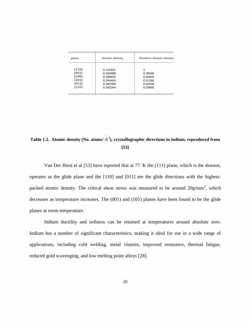
20
plane Atomic density Relative Atomic density
(110)
(001)
(100)
(101)
(012)
(110)
0.10431
0.09488
0.08830
0.06464
0.06269
0.06244
1
0.9606
0.8465
0.6196
0.6009
0.5985
Table 1.2. Atomic density (No. atoms/
A 3), crystallographic directions in indium, reproduced from
[53]
Van Der Biest et al [53] have reported that at 77 K the (111) plane, which is the densest,
operates as the glide plane and the [110] and [011] are the glide directions with the highest-
packed atomic density. The critical shear stress was measured to be around 20g/mm2, which
decreases as temperature increases. The (001) and (101) planes have been found to be the glide
planes at room temperature.
Indium ductility and softness can be retained at temperatures around absolute zero.
Indium has a number of significant characteristics, making it ideal for use in a wide range of
applications, including cold welding, metal vitamin, improved resistance, thermal fatigue,
reduced gold scavenging, and low melting point alloys [28].
21
1.2.3 Indentation Size Effect
A possible explanation of the indentation size effect (ISE) in materials was introduced by
Nix and Gao [29]. They declared that due to the strong strain gradient, which can either be
caused by loading geometry or inhomogeneous deformation in materials themselves, the
“geometrically necessary” dislocation density will be more pronounced in smaller-sized
materials [30]. Their model for strengthening smaller-sized materials was on the continuum basis
and could not predict the discrete displacement burst of materials at the very initial stage (less
than 100nm) of indentation depth sensing [31-36].
Constraining effects were present in most of the research that was conducted on the effect
of size on either bulk or thin film materials [36-41]. In order to exclude the constraining effect,
Greer et al [42] prepared some unconstrained freestanding gold pillars on which they conducted
a compression test. Using a uniaxial compression test in which a flat indenter tip was substituted
with the sharp Berkovich tip in the depth-sensing equipment, they were able to study strain
hardening in micro-pillars without the presence of a strong strain gradient. As a result, they have
stated that material strengthens inversely to its size even in the absence of a strong strain
gradient. In their approach they have related this strengthening to the dislocation starvation
condition, which is limited to small-volume samples. The nucleation of new dislocation seems to
be the most challenging for plastic mechanisms after the dislocation starvation condition [42-45].
Some other compression tests have been conducted on micro pillars of Ni, Al, Ni3AL, Cu, and
Mo alloy, all of which stated that the yield strength of material increased with decreasing in
pillar diameters [46-52].

22
Although the “dislocation starvation” theory explains the existence of discrete
displacements at the first stage of the indentation test, there is no unified theory that can explain
this size effect [42-45]. For example, while dislocation starvation seems to be the dominant
mechanism for plasticity in the FCC single crystals, it cannot be the central mechanism for the
BCC single crystals [51] or in metallic glasses, where size effect plasticity is also observed even
though they do not contain any dislocations [52].
1.3 Objective of the Work
Unlike most of the research that was limited to the study of monotonic deformation in
materials, the present work intends to investigate the effect of size on the creep behaviour of
materials at the submicron scale in the absence of strong strain gradient and the constrain effect.
To conduct ambient temperature compression testing, and skip the small displacement
associated with elevated temperatures, and also to reduce the testing time of the time-dependent
creep phenomenon, indium was selected as the testing metal.
Samples have been fabricated by two different methods in order to account for the effect
of fabrication method. To monitor the creep mechanism that is dominant in our testing, samples
have been characterized in two general ways: as single crystalline and polycrystalline samples.
The polycrystalline samples have been differentiated in such a way that they contain different
grain boundary sizes.
Further more to observe the creep behaviour of materials in the absence of strain gradient
plasticity a compression test was chosen in which the sharp Berkovich tip was substituted by a
flat diamond tip.

23
Chapter 2
Sample Design
2.1 Introduction
In order to gain insight into the deformation mechanism that leads to plasticity at the
micron and submicron scales, the present work developed the submicron indium samples to test
their creep behaviour in the absence of a strong strain gradient. The test methodology consisted
of fabricating the single-crystalline and poly-crystalline freestanding indium cylinders at
submicron dimensions. This chapter will introduce the sample design and also the techniques
that have been applied for fabricating the samples.
2.2 Sample Design
As mentioned above, the present work fabricates submicron-scale indium samples to test
their creep behaviour in the absence of strain gradient plasticity. To fulfill the objectives of the
mentioned topic, the sample design should satisfy three essential criteria outlined below.
First, the sample design should provide unconstrained geometry with a flat top. This
minimizes the effect of the strain gradients in the compression test. Based on this fact, the overall
view of the samples should be a flat top cylindrical unconstrained shape. Compared to other
shape features, cylinders have less strain gradient deformation during compression testing. A
schematic overall view of the sample was illustrated in Figure 2.1.

24
indium
substrate
Figure 2.1 Schematic of sample overall design
The second parameter is sample diameter. A reasonable range of diameters provides a
more realistic analysis of the effect of size in creep behaviour. For this reason, a range of
diameters from 100nm-10μm have been considered to provide reasonable data.
The third factor for categorizing the samples was the creep mechanism. The dominant
creep mechanism is dissimilar in single crystals and poly-crystals, so each sample size was
categorized into these two major groups. The poly-crystal pillars have also been grouped by
different grain boundary sizes in order to gain insight into their effect on creep behaviour at the
submicron scale. Figure 2.2 summarized the sample categorization based on the aforementioned
factors.

25
Single
crystal
105210.50.250.1
D(μm)
Crystal
Poly
crystals
3000
500
50
Single
crystal
Figure 2.2 Summery of sample design
2.3 Fabrication Techniques
Having the samples designed, the most difficult challenge is to then fabricate them. Many
researchers use focus ion beam (FIB) in their studies to fabricate freestanding submicron pillars
[42-52], meaning that the FIB is used as the first approach. This instrument is equipped with a
focused Ga + ion beam and a high-resolution field emission scanning electron column; both of
these features propagate a submicron precision etch on the sample surface.

26
Unfortunately, fabricating the indium submicron pillars using the FIB was not an
appropriate technique in this project because the indium metal was melted away by high-energy
Ga+ ions before forming the submicron diameter pillars. Therefore, the low melting point indium
metal limited the application of the FIB.
As a result, the microlithography and electroplating approach that is widely used in the
industrial fabrication of integrated circuits (ICs) was applied. A large number of indium pillars
with a predesigned diameter can be fabricated on a silicon substrate by this technique.
2.3.1 Focus Ion Beam Instrument
The focus ion beam (FIB) instrument resembles the secondary electron microscope
(SEM), with one major difference. In FIB, the ion beam is applied for analysis whereas an
electron beam is applied in SEM.
The main parts of the Focus Ion Beam instrument consist of liquid metal ions, an ion
column, a gas injector, and a sample stage, as illustrated schematically in Figure 2.3.

27
sample
Sample stage
Gas injector
Ion chamber
detector
Figure 2.3 Basic Focus Ion Beam instrument, reproduced from [54]
The main parts of the FIB instrument are the column ion and liquid metal ion source
(LMIS), where a gallium metal is attached to a tungsten needle and then heated. The gallium can
be replaced by different metals. However, some of the characteristics of gallium make it the best
choice for the LMIS. Some of these characteristics are [54]:
i) Low liquid volatility, which preserves the chamber longer
ii) Low melting point (29.8ºC) and low free-surface tension, which facilitate the formation
of the Taylor cone at the tungsten needle
iii) Low vapor pressure, which ensures the formation of a pure form of vapor rather than the
alloy component

28
The gallium ion is emitted through two steps; first, the gallium is heated and wets the tungsten
needle with a typical tip radius of 2-5 μm; second, an electric field of 108V/cm at the tip causes
the molten gallium to form a 2-5nm diameter Taylor cone. Once the electrostatic and surface
tension forces are in balance, the extraction voltage pulls the gallium off the needle and ionizes it
at the cone end. Once the Ga+ has left the tip, it will accelerate through the potential down the
ion column. The continuation of this process will increase the current density. A typical
accelerating voltage is about 5-50 kv.
The ion column consists of two lenses; (1) a condenser lens, which is probe-forming, and
(2) an objective lens, which focuses the ion beam onto the target (sample surface). The current
range can be varied from a few pA to 20-30 nA for various applications by various diameter
apertures in the ion column.
When the Ga+ strikes the sample surface, many species will be generated, including
sputtered atoms, molecules, secondary electrons, and secondary ions [54].
2.3.1.1 The Stage
The sample stage has the ability to move in five axis directions. It is important to ensure
that the large stage (>300mm samples) is thermally stable and that no heat will be generated
because of its mechanical motion. This will avoid thermal drift in the sample during FIB imaging
or deposition.

29
2.3.1.2 Imaging Detector
Two types of detectors are used for imaging the sample surface. One is a multichannel
plate and the other is a multiplier that can be set for detecting either the secondary electrons or
the secondary positive ions.
2.3.1.3 Gas Injectors
The FIB instrument can also be applied to micromachining applications and thin-film
deposition. This ability of FIB systems was facilitated by the existence of gas injectors. Gas
direction will be applied in conjunction with ion beams to produce a specified site for material
deposition or insulator to enhance etching capability. Additionally, the sputtering rate can be
facilitated by introducing specific species to the chamber [54].
Commercial FIB systems are equipped with some other analytical equipment such as the
secondary ion beam (SIB), energy dispersive spectrum (EDS), integrating electron backscatter
diffraction (EBSD) and secondary ion mass spectrometer (SIMS) and secondary electron microscope
(SEM). The FIB/SEM is the most common dual platform out of all the aforementioned equipments
[54].
30
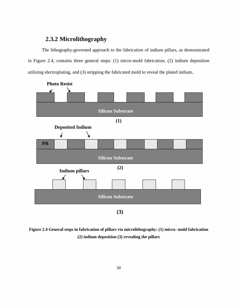
2.3.2 Microlithography
The lithography-governed approach to the fabrication of indium pillars, as demonstrated
in Figure 2.4, contains three general steps: (1) micro-mold fabrication, (2) indium deposition
utilizing electroplating, and (3) stripping the fabricated mold to reveal the plated indium.
Figure 2.4 General steps in fabrication of pillars via microlithography: (1) micro- mold fabrication
(2) indium deposition (3) revealing the pillars
(1)
PR
(2)
Silicon Substrate
Silicon Substrate
Silicon Substrate
Deposited Indium
Indium pillars
Photo Resist
(3)

31
2.3.2.1 Micro- Mold Fabrication
The first step in the fabrication of micro-mold chips is to design the mold pattern,
followed by the development of a fabrication process for the desired pattern.
2.3.2.1.1 Micro-Mold Chips Design
The design pattern of micro-mold chips consists of a patterned mold with a controlling
surface and a conductive surface. The patterned mold section consists of circular shape features
whose diameters correspond to the diameters of the pillar samples. A fixed controlling surface
was considered for the chips in order to provide a steady-state current density during the
electroplating deposition process. The controlling surface was arranged in an array form having
sub-micron width, which is in approximate with the indium growing pillars diameter. This
improves current distribution during the plating process. A conductive surface was designed for
the chips in order to pass the current to the indium deposition sites during the electrodepositing
process. The size of the mold-chip was chosen 2.54 x 2.54 cm in accordance with the available
photo-masks. The bottom surface of all the mentioned patterns must be coated with a good
conductor, such as gold, in order to pass the current for indium deposition. The overall design of
the mold is illustrated in Figure 2.5.
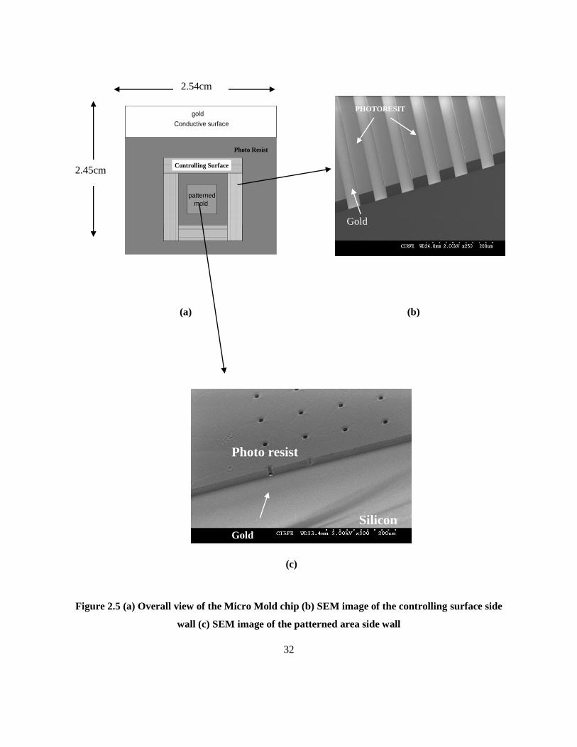
32
patterned
mold
Conductive surface
Photo Resist
Controlling Surface
gold
(a) (b)
(c)
Figure 2.5 (a) Overall view of the Micro Mold chip (b) SEM image of the controlling surface side
wall (c) SEM image of the patterned area side wall
PHOTORESIT
Silicon
Silicon
2.45cm
2.54cm
Gold
Gold
Photo resist

33
2.3.2.1.2 Micro-Mold Fabrication Process
The micro-mold is a shaped mold upon which the indium is filled. Photolithography is
applied to project the designed pattern onto the chip surface. In this process, a light-sensitive
material known as a photo resist, usually in liquid form, is spun on the wafer surface by spin
coating. Spinning the photo resist will form a film whose thickness depends directly on the spin
speed and the duration of spinning. The wafers are heated through a process, known as the soft
bake. The soft bake step drives the solvent off of the photo resist and leaves a solid photo resist
layer on the wafer. The wafer is then exposed to an appropriate dosage of ultraviolet (UV) light,
or electron-beam for higher resolution patterning. The exposure process causes a chemical
reaction in the photo resist which alters its solubility in the developer. The photo resist can either
be positive or negative. Chemical reactions cause the negative photo resist to become less
soluble in the developer while they make the positive photo resist become more soluble in the
developer. The wafer is then developed, and the unwanted resist is removed while the desired
patterns remain.
The main steps for fabricating the mold are:
1. Coating the substrate with gold as the conductor medium
2. Spin coating the chrome/gold surface with a photo resist
3. Lithographically patterning the photo resist
4. Developing the photo resist in a developer

34
1.substrate
2.Coating chrome/ gold
3.Coating photo resist
4.Patterning with lithography
5.Developing the photo resist
Substrate
Chrome/Gold
seed layer
Photo resist
Not-exposed PR
Exposed PR
Indium
deposition
site
Figure 2.6 Steps for fabrication of micro-mold
The detailed procedure of micro-mold fabrication will be discussed in the next chapter.
2.3.2.2 Electro-Depositing
Electroplating, which is widely used in microelectromechanical systems (MEMS)
fabrications, was applied for indium deposition. Electroplating was chosen for use in the
deposition process because it provides excellent characteristics such as refined grain structure,
smoothness and low residual stress, to the deposited material [55-60]. In addition to the quality
of the plating, the ability to coat thin layers using low-cost procedures means that electroplating
is preferred over other methods of deposition [59].
35
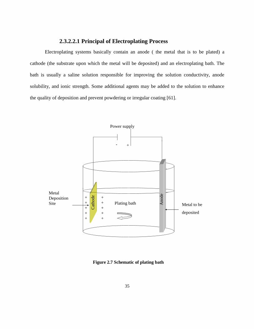
2.3.2.2.1 Principal of Electroplating Process
Electroplating systems basically contain an anode ( the metal that is to be plated) a
cathode (the substrate upon which the metal will be deposited) and an electroplating bath. The
bath is usually a saline solution responsible for improving the solution conductivity, anode
solubility, and ionic strength. Some additional agents may be added to the solution to enhance
the quality of deposition and prevent powdering or irregular coating [61].
Cat
ho
de
An
od
e
Plating bath
+
+
+
+
+
- +
Power supply
+
+
+
+
+
Metal
Deposition
Site Metal to be
deposited
Figure 2.7 Schematic of plating bath
36
During electroplating, some variables such as current density, agitation, temperature, and
pH affect the physical characteristics of the deposited material and also the deposition rate of the
plating [61].
2.3.2.2.2 Current Density
Current density, which is the amount of current passing through 1cm2
of
area, can be
examined from two points of view: (1) diffusion control, or (2) cathode potential [61].
1) Diffusion control refers to the movement of ions in the solution as a result of
concentration gradient. Diffusion is the consequence of random molecular motions which
distribute the various specimens uniformly throughout the solution. Depletion ions in the
anode will produce ion gradient concentration in the solution, resulting in the movement
of these specimens from the anode towards the cathode.
2) Potential control is established when both the anode and cathode are connected to an
external power supply and an electric field is established in the bath. This field will lead
the ions, having a positive charge, towards the cathode. The electrical current will then
reduce the anode and coat the material on a conductive object (cathode) in the form of a
thin layer.
The effect of current density on the deposition rate is very much dependent on the plating
system, and can be altered by agitation, changing the pH, temperature, and some other factors.
Therefore, there is no universal rule for measuring its influence on the deposition rate.
Indium was applied as the anode in the plating system and the micro-mold chip as the
cathode. A range of different values for the current density was tested and the optimal current
37
density which satisfies the high-quality deposition for the plating system chosen. Deposition
rates can be calculated from the deposited thickness and the duration of plating.
Using the Faraday’s Law equation [62], thickness can be estimated by the current density
applied and the duration of the plating process. Faraday’s equation is:
nF
AtMm 2-1
Where m is the transferred mass from the anode to cathode (g), A is current (A), M is molecular
weight (g), n is the number of the transferred electron, F is Faraday constant and η is efficiency.
2.3.2.3 Revealing the Pillars
After plating the indium, the next step is to remove the sacrificial layer to reveal the
pillars. In this step, depending on the kind of resist that was applied, a resist remover is chosen to
strip unwanted surfaces. Freestanding indium pillars will be released during this step. Figure 2.8
illustrates some of the pillars fabricated using the microlithography approach.

38
D=257nm
Indium
Gold
Indium deposition site
Indium pillar
D=369nm
h=777.9nm
Indium
GoldD=359.2nm
h=758nm
Indium
Gold
Figure 2.8 SEM image of fabricated pillars via micro lithography
39
Chapter 3
Sample Fabrication
3.1 Introduction
Sample preparation is one of the greatest challenges in this work because a versatile
sample diameter and category must be considered. Equipment availability was also a limiting
parameter. The fabrication procedure was conducted in the MEMS facility of the Centre for
Integrated RF Engineering (CIRFE) at the University of Waterloo. Fabrication of the designed
samples was performed based on the available equipment and facilities.
Although the micro-fabrication method was widely applied during the past decade, there
is no unified procedure to be followed in the fabrication of each sample design. As a result,
processes need to specifically develop for each design.
This chapter shares invaluable experience that was achieved during the development of a
microlithography process for making freestanding submicron pillars. The process is based on
using indium as our testing metal. This chapter will also cover the results and the detailed
development procedure and the related characterizations in fabrication of different pillar
diameter.
3.2 Sample Fabrication
As mentioned in section 2.3, the first approach to FIB was applied in the fabrication of
the pillars. The low melting point of indium limited its fabrication using FIB therefore

40
microlithography was developed. The following two sections will present the results of the two
fabrication techniques.
3.2.1 Sample Fabrication using the Focused Ion Beam (FIB)
To fabricate the patterns of interest, a Leo/Zeiss 1540XB SEM/FIB Crossbeam at the
Nanofabrication Laboratory of the University of Western Ontario was used. The ion dose,
expressed in μC/cm2, controlled the amount of material sputtering from the surface. A deeper
mill can be achieved by employing a higher dose of beam, which irradiates a larger number of
high-energy ions onto the sample surface. This will cause more ions to sputter from the surface.
The ion current (C/sec) controls the rate at which the required dose of ions are transmitted to the
specimen. Although a higher current gives faster milling which requires less time and lower
operating costs, it causes less focus in the beam by adding a tail to it which decreases the
precision in the milled area. The applied accelerating voltage and beam angle are based on
previous experience in the lab and were not changed. The applied accelerating voltage was 30kV
and the beam angle was 90º throughout the experiment.
The FIB process was conducted on well-annealed single-crystal indium. The indium slab
was first annealed at 100C for two hours in an oven and polished by electro-polishing.
The applied electropolishing solution was a 3:1 mix of methanol and nitric acid with a
voltage of 32v at 0C [24]. The anode was a 3.8 x 2.54 cm indium slab with the thickness of ~2
mm and the cathode was a 14 cm x 3 cm graphite bar.
For any further polishing, another solution with a lower voltage and better quality of
surface polishing was applied. This polishing condition was based on the work of Schoeller and

41
Cho. With a 1:3 mix of nitric acid and ethanol and a voltage of 4v [63], Based on this recipe, the
polishing rate was calculated to be 100nm/sec.
3.2.2 Focus Ion Beam Fabrication Results
The first step in the fabrication process was selecting an appropriate section of the sample
for machining. It is important to ensure that the selected surface has very few particles and is
smooth, as any surface roughness will result in non-uniform etching.
In the FIB instrument, the stage and sample are adjusted to the eucentric position, where
the ion beam and the electron beam are focused with the same working distance that usually
equals 6mm. The sample is then tilted to 52.7 with respect to the electron detector.
When milling the surface to the desired geometry, it is required that the pillars be
surrounded by a crater. As a result, the crater is milled first and then the pillar is created in its
centre by sequential etching of concentric circles with smaller and smaller inner diameters.
Having the pillar in the crater helps to prevent the indenter tip from misaligning and coming into
contact with other features, such as the edges, during the compression test [52].
Current of Ga+ ion of 2000 pA with 500 μC/cm² dosages was applied to mill out the 30
μm crater in the material and then leave a 10 μm diameter pillar in the center, as illustrated in
Figure 3.1.

42
Table 3.1 Milling condition of 10 μm pillar with FIB
Current
PA
Voltage
Kv
Crater diameter
μm
Tilt angle Diameter
μm
Dosage
μC/cm²
2000 30 30 52.7 10 500
D=11.64μm
Indium
Indium
Figure 3.1 I-Beam image of 10 μm pillars. Crater size is 30 μm. Current was 2000 pA, and dosage
was 500 μC /cm²
During fabrication of the smaller-diameter samples, two sets of dosages were applied;
first, from 30 μm to 5μm diameter, a dosage of 500 μC/cm² with 1000 pA ion current was
applied, and then from 5 μm to 3μm a lower dosage of 100 μC/cm² with 1000 pA Ion current
was used.
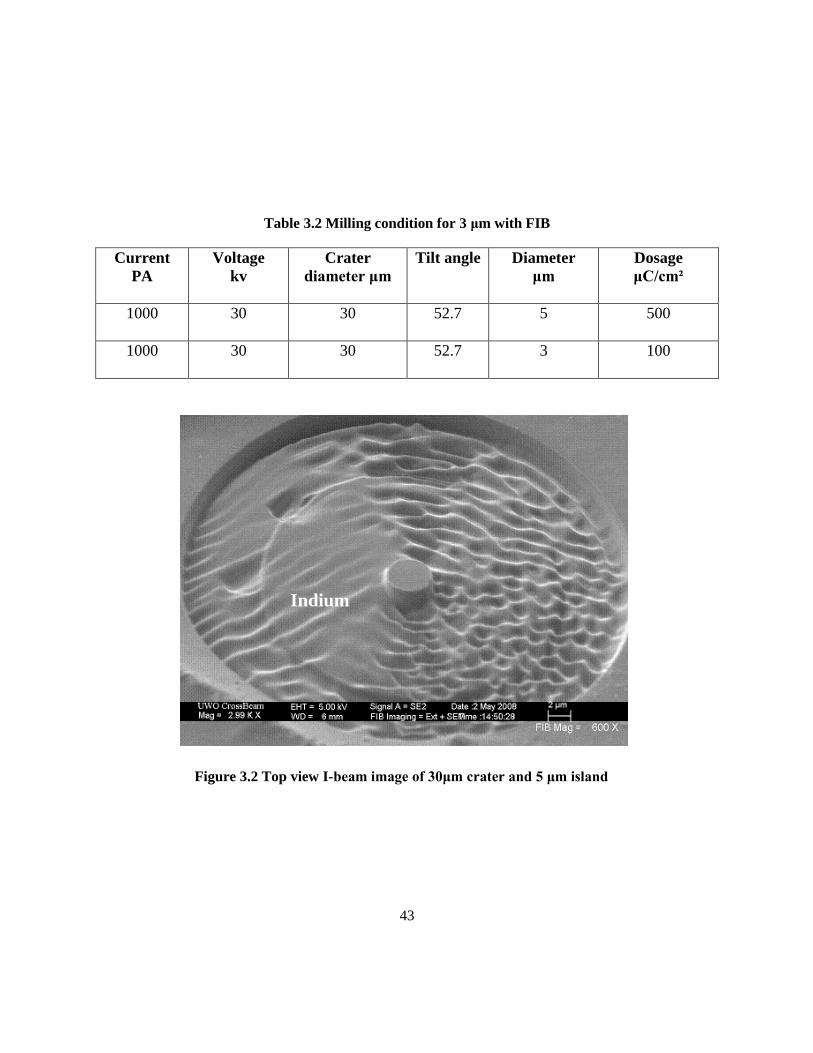
43
Table 3.2 Milling condition for 3 μm with FIB
Current
PA
Voltage
kv
Crater
diameter μm
Tilt angle
Diameter
μm
Dosage
μC/cm²
1000 30 30 52.7 5 500
1000 30 30 52.7 3 100
Figure 3.2 Top view I-beam image of 30μm crater and 5 μm island
Indium

44
Figure 3.3 I-beam image of FIB fabricated pillar having a diameter of 2.85 μm
As can be seen in Figure 3.3, during the fabrication of finer feature samples even a low
dosage of Ga+ will melt away the indium metal before forming it, which is due to the low
melting point of indium. Some other challenges were also observed, such as base trench
formation, pillar tapering, and also possible Ga+ implantation into the indium samples. As the
diameter of the concentric circles becomes smaller, the pillars become more tapered. This
tapering is mainly due to the I-beam imaging that causes some inevitable etching which is
negligible for larger features but becomes an important concern for the smaller-diameter pillars
(<3μm). Although applying a set of different currents and dosages may improve the structure of
the formed pillars, the cost of fabrication and the unavailability of these facilities on campus
limited led the use of an alternative technique which is essentially based on lithographic micro
fabrication.
Melted area
Indium
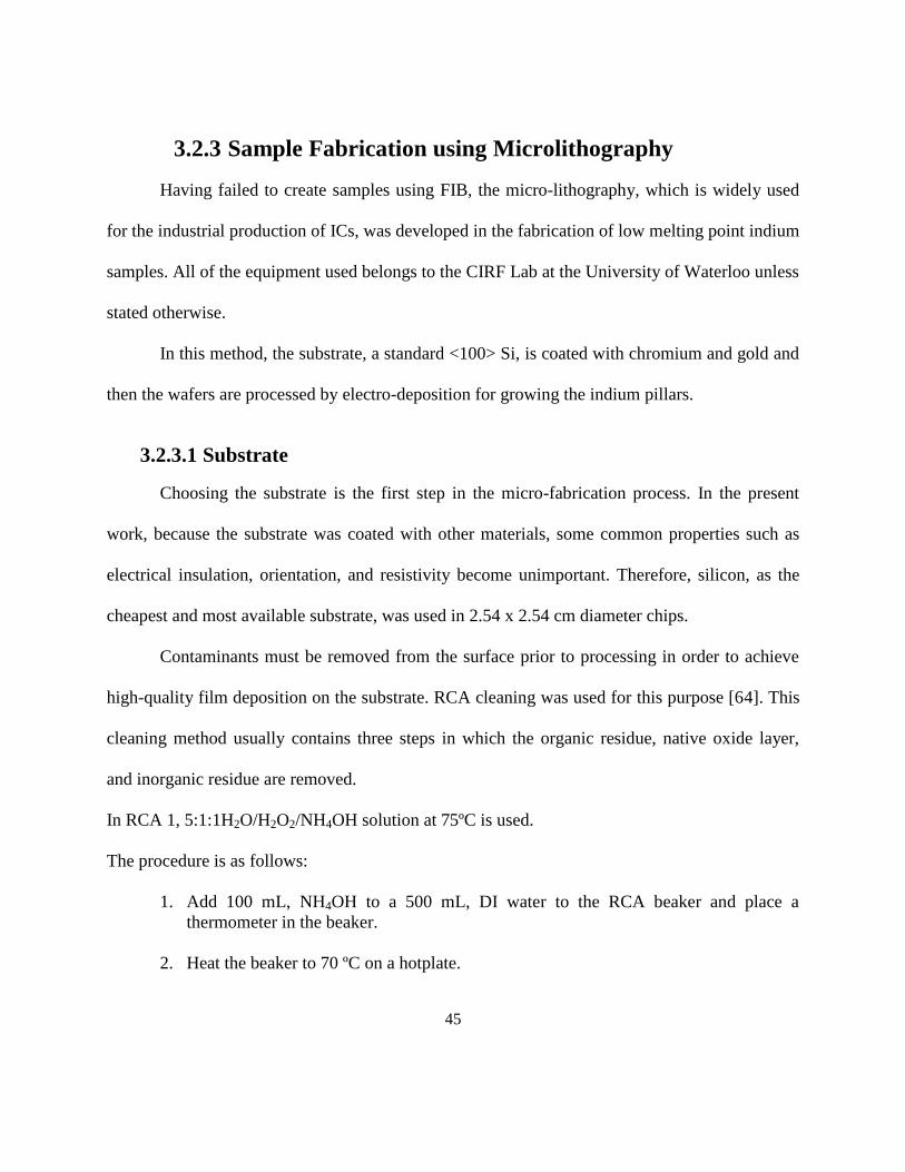
45
3.2.3 Sample Fabrication using Microlithography
Having failed to create samples using FIB, the micro-lithography, which is widely used
for the industrial production of ICs, was developed in the fabrication of low melting point indium
samples. All of the equipment used belongs to the CIRF Lab at the University of Waterloo unless
stated otherwise.
In this method, the substrate, a standard <100> Si, is coated with chromium and gold and
then the wafers are processed by electro-deposition for growing the indium pillars.
3.2.3.1 Substrate
Choosing the substrate is the first step in the micro-fabrication process. In the present
work, because the substrate was coated with other materials, some common properties such as
electrical insulation, orientation, and resistivity become unimportant. Therefore, silicon, as the
cheapest and most available substrate, was used in 2.54 x 2.54 cm diameter chips.
Contaminants must be removed from the surface prior to processing in order to achieve
high-quality film deposition on the substrate. RCA cleaning was used for this purpose [64]. This
cleaning method usually contains three steps in which the organic residue, native oxide layer,
and inorganic residue are removed.
In RCA 1, 5:1:1H2O/H2O2/NH4OH solution at 75ºC is used.
The procedure is as follows:
1. Add 100 mL, NH4OH to a 500 mL, DI water to the RCA beaker and place a
thermometer in the beaker.
2. Heat the beaker to 70 ºC on a hotplate.

46
3. Clean the sample wafers with DI water and/or acetone and dry them with a nitrogen
gas gun. Place them in a wafer holder.
4. At 70 ºC, pour 100 mL of hydrogen peroxide into the solution while a magnetic stirrer
is stirring it.
5. Submerge the wafer with a wafer holder in to the beaker and heat it for 15 minutes.
6. Prepare 700ml of DI water in the hot water bath beaker and heat it to ~ 80-90ºC on a
separate hotplate. Cover the beaker with a lid.
7. After 15 minutes, remove the wafer holder. put it in a hot bath beaker, and heat it for
another 15 minutes.
8. Wash the beaker under running DI water.
9. Blow dry the wafer with nitrogen gas.
In the RCA1, heating the wafers in a high-pH solution will remove organic contaminants
by oxidative dissolution while heavy metals dissolve, form a complex, and are rinsed away with
DI water. In the RCA2, the inorganic contaminants can be removed in the low-pH solution using
H2O/H2O2/HCL. In the RCA3, submerging the silicon wafers in the dilute HF solution will
remove the thin oxide layer. As the effect of inorganic contaminants and the oxide layer are
negligible, only RCA1 was applied.
3.2.3.2 Gold & Chromium Deposition
The next step is to coat the substrate with a highly conductive metal. Gold was chosen as
a conductive medium because it does not adhere to silicon. Silicon must be the first to be
deposited, with chromium as a middle layer, followed by gold. The thickness of each layer must
be large enough to give a uniform surface.

47
The Cr/Au deposition took place in a NanochromeTM
DC sputtering system (Intelvac,
Canada). In this vacuum sputter chamber, the E-beam gun, having a power range from 6 to 208
kW, focuses and accelerates the E-beam towards the target (the metal). A certain percentage of
the kinetic energy from the E-bean is converted into thermal energy, which melts the metal ingot.
Since the chamber is under a highly-vacuum the metal will evaporate and be deposited on the
substrate. Following deposition, a shutter blocks the E-beam gun and the metal cools to room
temperature, which takes approximately ten to fifteen minutes.
3.2.3.2.1 E-beam Evaporation Deposition
Substrate
Substrates are fixed manually in the substrate holder at six spots. The maximum size of
the substrate should be less than five inches in diameter. The substrate face on which deposition
is being performed should face down.
Material deposition
The materials that get deposited are placed in a copper crucible in the form of an ingot. A
pocket controller controls a shaft and places the metal under the E-Beam gun. It is important to
mix the ingot before each deposition to bring up the fresh metals from the underneath
Vacuum chamber
Cryogenic pump is used to create the vacuum in the chamber by using helium as a
refrigerant. The cryogenic temperature has to reach 10.9K and the vacuum pressure must be at
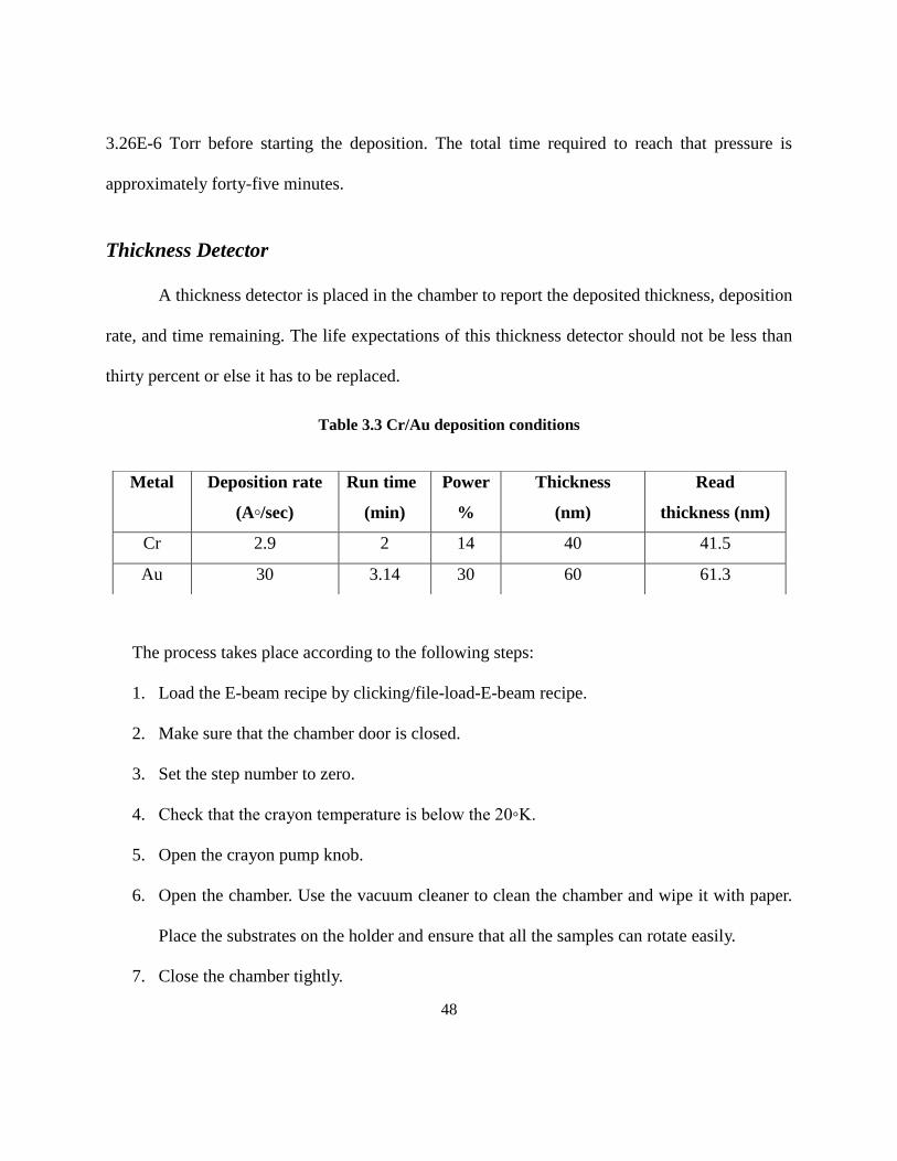
48
3.26E-6 Torr before starting the deposition. The total time required to reach that pressure is
approximately forty-five minutes.
Thickness Detector
A thickness detector is placed in the chamber to report the deposited thickness, deposition
rate, and time remaining. The life expectations of this thickness detector should not be less than
thirty percent or else it has to be replaced.
Table 3.3 Cr/Au deposition conditions
The process takes place according to the following steps:
1. Load the E-beam recipe by clicking/file-load-E-beam recipe.
2. Make sure that the chamber door is closed.
3. Set the step number to zero.
4. Check that the crayon temperature is below the 20K.
5. Open the crayon pump knob.
6. Open the chamber. Use the vacuum cleaner to clean the chamber and wipe it with paper.
Place the substrates on the holder and ensure that all the samples can rotate easily.
7. Close the chamber tightly.
Metal Deposition rate
(A/sec)
Run time
(min)
Power
%
Thickness
(nm)
Read
thickness (nm)
Cr 2.9 2 14 40 41.5
Au 30 3.14 30 60 61.3

49
8. Press the pump command in the software. Wait for approximately forty minutes for the
chamber to be vacuumed.
9. On the chamber machine, press menu-review-process, go to edit-change to change steps,
thickness, and depositing material. Correspondingly set step 1, thickness: 40nm, material:
chromium and step 2, thickness of 60nm, material: gold.
10. Press status to check the life of the thickness detector, it should be more than thirty
percent.
11. If the pressure is around 3.26E-6 torr and the crayon temperature is around 10.9K. Turn
on the power supply and then press the on (green) button so that the deposition will start.
12. After the deposition is complete, wait for approximately fifteen minutes for the material
to cool down and then remove the samples.
.
Table 3.4 Supplementary conditions for Cr/Au deposition
3.2.3.3 Types of Microlithography
As discussed earlier, the samples of the present work were characterized by diameter. As
sample diameters decrease, the resolution and accuracy of the process become more crucial and
directly affect the developing process. From this point, the samples have been fabricated by two
Life of
thickness
detector
Chamber pressure
(Torr)
Vacuum
time (min)
Crayon temperature
(K)
69% 6.26E-6 45 11.2
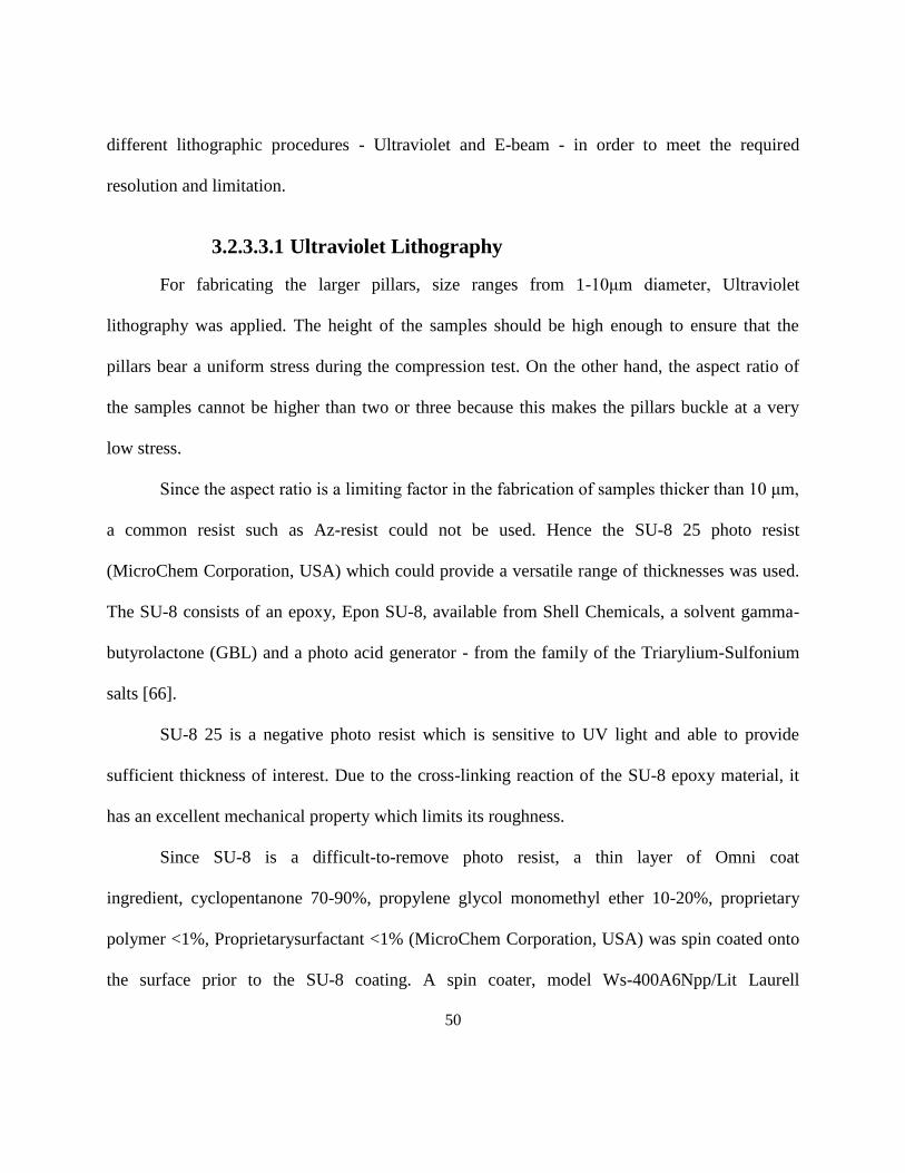
50
different lithographic procedures - Ultraviolet and E-beam - in order to meet the required
resolution and limitation.
3.2.3.3.1 Ultraviolet Lithography
For fabricating the larger pillars, size ranges from 1-10μm diameter, Ultraviolet
lithography was applied. The height of the samples should be high enough to ensure that the
pillars bear a uniform stress during the compression test. On the other hand, the aspect ratio of
the samples cannot be higher than two or three because this makes the pillars buckle at a very
low stress.
Since the aspect ratio is a limiting factor in the fabrication of samples thicker than 10 μm,
a common resist such as Az-resist could not be used. Hence the SU-8 25 photo resist
(MicroChem Corporation, USA) which could provide a versatile range of thicknesses was used.
The SU-8 consists of an epoxy, Epon SU-8, available from Shell Chemicals, a solvent gamma-
butyrolactone (GBL) and a photo acid generator - from the family of the Triarylium-Sulfonium
salts [66].
SU-8 25 is a negative photo resist which is sensitive to UV light and able to provide
sufficient thickness of interest. Due to the cross-linking reaction of the SU-8 epoxy material, it
has an excellent mechanical property which limits its roughness.
Since SU-8 is a difficult-to-remove photo resist, a thin layer of Omni coat
ingredient, cyclopentanone 70-90%, propylene glycol monomethyl ether 10-20%, proprietary
polymer <1%, Proprietarysurfactant <1% (MicroChem Corporation, USA) was spin coated onto
the surface prior to the SU-8 coating. A spin coater, model Ws-400A6Npp/Lit Laurell

51
Technologies Corporation, USA) was applied for spin coating the Omni coat. After this process,
the wafers were heated for three minutes at 200C in a Lindberg/blue Man Del High Temperature
Bake Oven (Thermal Product Solution (TPS) Company, USA). This allows for the fast and easy
removal of SU-8 during the developing process.
Here are the steps for coating the wafers with Omni coat:
1. Shake the Omni coat solution.
2. Clean the spin coater and holder as well as all the edges.
3. Clean the chips in a dilute acetone, blowing nitrogen gas to dry them. Hold the chips tight.
4. Place the silicon wafer on the chip holder.
5. Press the vacuum button to vacuum hold the wafers.
6. Place 3-4 droplets of Omni coat onto the wafers with a 10 mL syringe.
7. Based on previous experiments in which the device setting could coat 17nm thickness at
4000rpm/sec speed and twenty-second duration. A spin speed of 2000 rpm and duration of
twenty seconds should take in approximately 30nm of thickness.
Table 3.5 Omni coat spin coating conditions
Acceleration
rate(rpm/sec)
Time
(s)
Thickness
(nm)
Speed
(rpm)
1215 20 30 2000
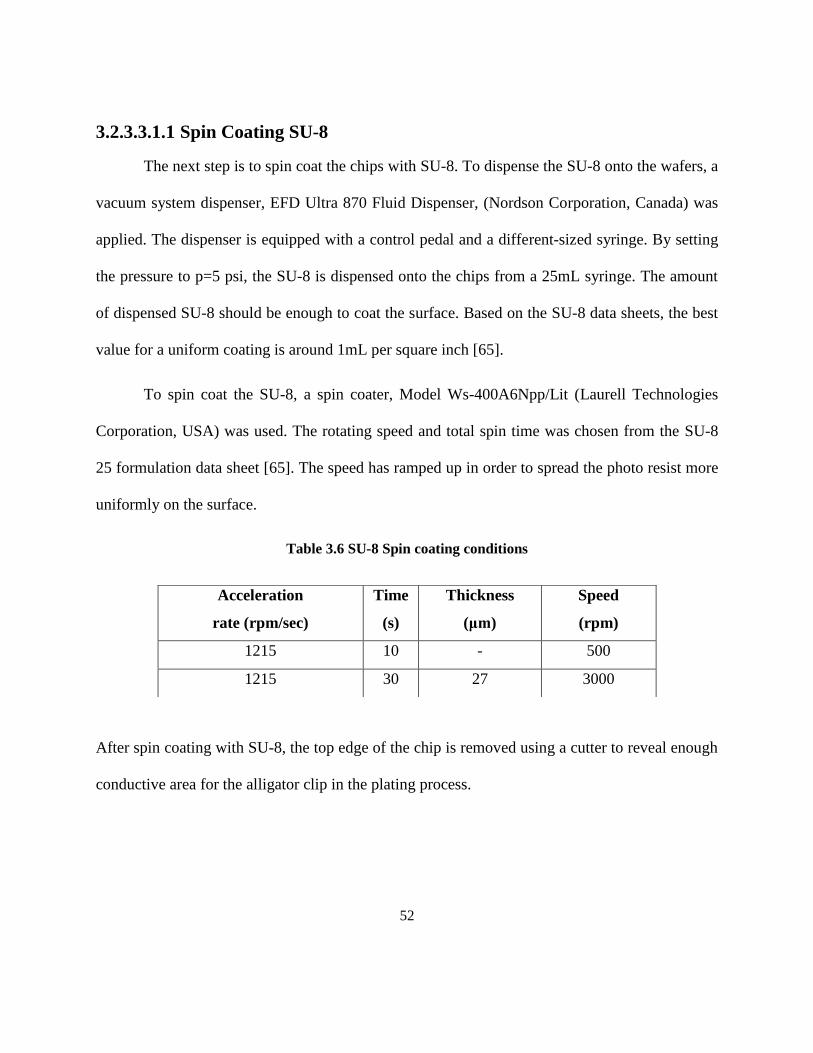
52
3.2.3.3.1.1 Spin Coating SU-8
The next step is to spin coat the chips with SU-8. To dispense the SU-8 onto the wafers, a
vacuum system dispenser, EFD Ultra 870 Fluid Dispenser, (Nordson Corporation, Canada) was
applied. The dispenser is equipped with a control pedal and a different-sized syringe. By setting
the pressure to p=5 psi, the SU-8 is dispensed onto the chips from a 25mL syringe. The amount
of dispensed SU-8 should be enough to coat the surface. Based on the SU-8 data sheets, the best
value for a uniform coating is around 1mL per square inch [65].
To spin coat the SU-8, a spin coater, Model Ws-400A6Npp/Lit (Laurell Technologies
Corporation, USA) was used. The rotating speed and total spin time was chosen from the SU-8
25 formulation data sheet [65]. The speed has ramped up in order to spread the photo resist more
uniformly on the surface.
Table 3.6 SU-8 Spin coating conditions
After spin coating with SU-8, the top edge of the chip is removed using a cutter to reveal enough
conductive area for the alligator clip in the plating process.
Acceleration
rate (rpm/sec)
Time
(s)
Thickness
(μm)
Speed
(rpm)
1215 10 - 500
1215 30 27 3000

53
3.2.3.3.1.2 SU-8 Soft Bake
The chips are heated up to 95C using a hotplate1000-1 (Electronic Micro System Ltd,
UK). The soft baking process lets the solvent of the SU-8 evaporate at the surface. As a result,
the SU-8 becomes more sensitive to the UV light and also makes the SU-8 stick firmly to the
substrate. Over-baking the samples will stiffen the SU-8 in such a way that developing it
becomes difficult.
Baking SU-8 on the hotplate is important because the heat will increase from bottom to
top, in contrast with the oven where a firm surface layer will form prior to the bottom parts
therefore the solvent cannot escape at the surface. The temperature ramp will slow down the
solvent evaporation, which improves the quality of surface and resists adhesion [65].
Table 3.7 SU-8 soft bake Conditions
3.2.3.3.1.3 Chromium Photo Mask
To pattern the SU-8 resist, its surface is exposed to Ultraviolet light through a photo
mask. Because the black-and-white spectrum of opaque material in the chromium mask gives a
superior patterning resolution when compared with an emulsion mask, the chromium photo mask
Temperature (C) Time (min)
65 3.30
95 5.30

54
was preferred over the emulsion photo mask, even though its fabrication equipment was
unavailable at UW.
The original pattern of the mask was designed using the Corel Draw software and then
sent out to the University of Alberta for fabrication. Figure 3.4 illustrates the design pattern of
chromium mask ranging from 1-40 μm diameter size, corresponding to the size of the pillars.
20 μm 40μm
2 μm 5μm
3 μm
5 μm1μm
8μm10 μm8 μm
15 μm 12 μm
Figure 3.4 Schematic over view design of chromium mask fabricated at University of Alberta
Chromium Photo Mask Batches
Each of the illustrated black patterns on the chromium mask contains circular shape
patterns whose diameter corresponds with the diameter of the pillars and the controlling surface
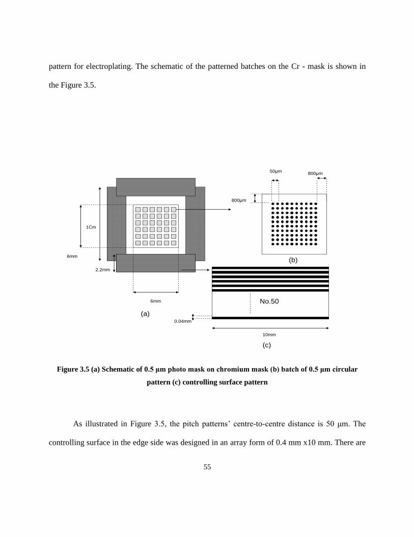
55
pattern for electroplating. The schematic of the patterned batches on the Cr - mask is shown in
the Figure 3.5.
6mm
(c)
1Cm
2.2mm
6mm
0.04mm
(a)
50μm
(b)
800μm
800μm
10mm
No.50
Figure 3.5 (a) Schematic of 0.5 μm photo mask on chromium mask (b) batch of 0.5 μm circular
pattern (c) controlling surface pattern
As illustrated in Figure 3.5, the pitch patterns’ centre-to-centre distance is 50 μm. The
controlling surface in the edge side was designed in an array form of 0.4 mm x10 mm. There are

56
fifty arrays each side. The total number of circular pattern batches is thirty-six, each of which
have one hundred circular patterns.
3.2.3.3.1.4 Ultraviolet Exposure on SU-8 Resist
SU-8 is patterned by exposing Ultraviolet light through a chromium photo mask. In SU-8
as a negative photo resist, the exposed parts will be insoluble in the SU-8 developer.
An Oriel mask aligner (Newport Corporation, USA) was used for exposing Ultraviolet
light. This aligner is equipped with a 500W ultra-filtered mercury lamp with 41 mW/cm2
intensity. The optimized dosage of 1800 mJ/cm2 was discovered experimentally through trial-
and-error. During this process, glycerol was injected into the gap between the photo mask and
the wafers to improve the quality of patterning. A brief explanation of its effect will be provided
in the following chapter.
Here are the steps for exposing the UV light in the aligner:
1. Place the Cr mask in the photo mask holder and fasten it.
2. Cut a piece of a blank Mylar and place it on the substrate wafer holder where the chips will
be placed; this will prevent vacuum leakage.
3. Place the chip in a manner to be aligned with the desired pattern on the chromium mask.
This can be done either manually or by the aligner adjustments.
4. Dispense four or five drops of glycerol with a 3 ml syringe.
5. Adjust the mask on the chips. Fasten it firmly until the glycerol spread on chip surfaces.
6. Vacuum the mask with a vacuum pressure of ~5 inHg.
7. Place the mask holder under the UV lamp.
8. Place i/liner filters to filter the wavelength below 360 nm.

57
9. Set dosage to 1800 mJ/cm2 and expose UV light
.
10. Spin coat chips in the spin coater at 2500 rpm for twenty seconds to remove the glycerol
from the SU-8 surface.
3.2.3.3.1.5 SU-8 Post-exposure Baking
Post-exposure baking on a hot plate will promote a cross-linking reaction in the SU-8
polymer resin. Since SU-8 is a negative photo resist, the cross-linking polymers will not be
soluble in the SU-8 developer. The temperature ramp is preferred in order to reduce stress and
cracking [65].
Table 3.8 SU-8 post exposure bake conditions
Temperature (C) Time (s)
65 3.5
95 6.5
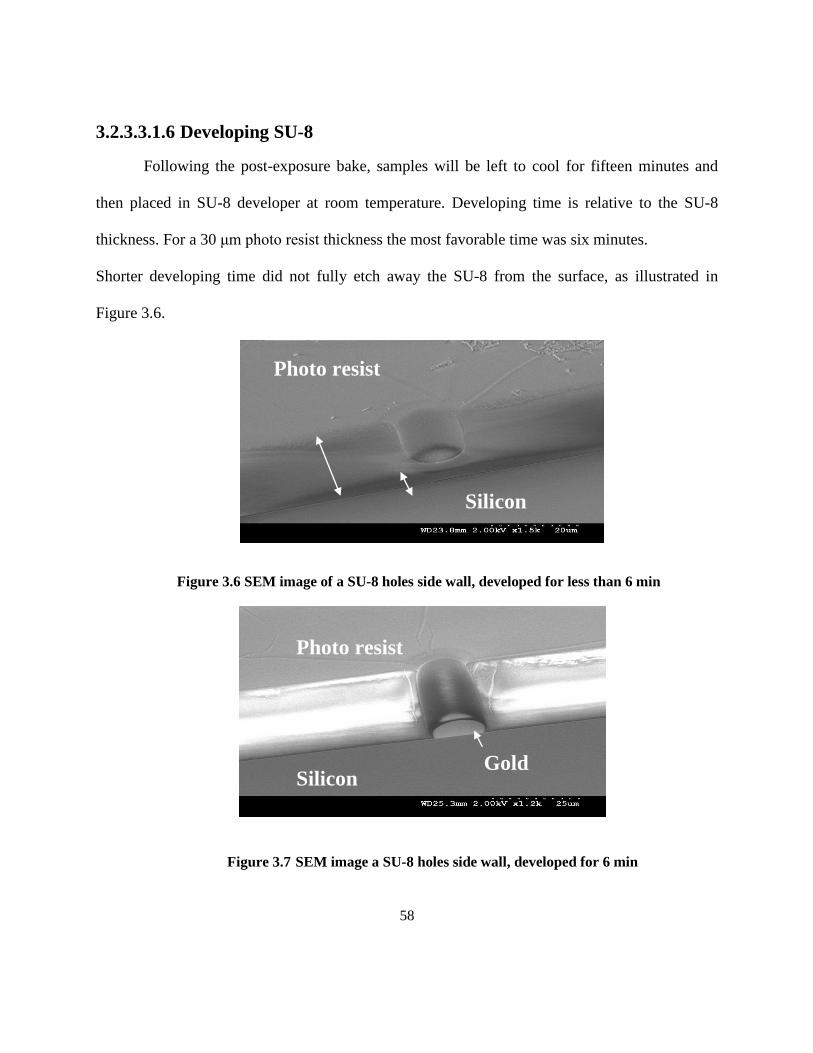
58
3.2.3.3.1.6 Developing SU-8
Following the post-exposure bake, samples will be left to cool for fifteen minutes and
then placed in SU-8 developer at room temperature. Developing time is relative to the SU-8
thickness. For a 30 μm photo resist thickness the most favorable time was six minutes.
Shorter developing time did not fully etch away the SU-8 from the surface, as illustrated in
Figure 3.6.
Figure 3.6 SEM image of a SU-8 holes side wall, developed for less than 6 min
Figure 3.7 SEM image a SU-8 holes side wall, developed for 6 min
Silicon
Gold
Photo resist
Silicon
Photo resist

59
After patterning the SU-8, the Omni-coat was etched from the surface by oxygen plasma
etching using a Trion Orion plasma-enhance chemical vapor deposition (PECVD) system (Trion
Technology, USA). The total applied time was sixty to ninety seconds at inductive coupled
plasma (ICP) of 20 watts, reactive ion etch (RIE) of 20 watts, pressure of 20mtorr, oxygen flow
of 40 sccm, and RIE reflect of 3 watts.
Figure 3.8 illustrates the SEM image of the controlling surface and Figure 3.9 illustrates
the patterned area in the UV lithography micro-mold chips.
Silicon
Photo R
esist
Gold
Silicon
Gold
Photo R
esist
(a) (b)
Figure 3.8 (a-b) SEM image of controlling surface side wall on a UV-micro-mold chip
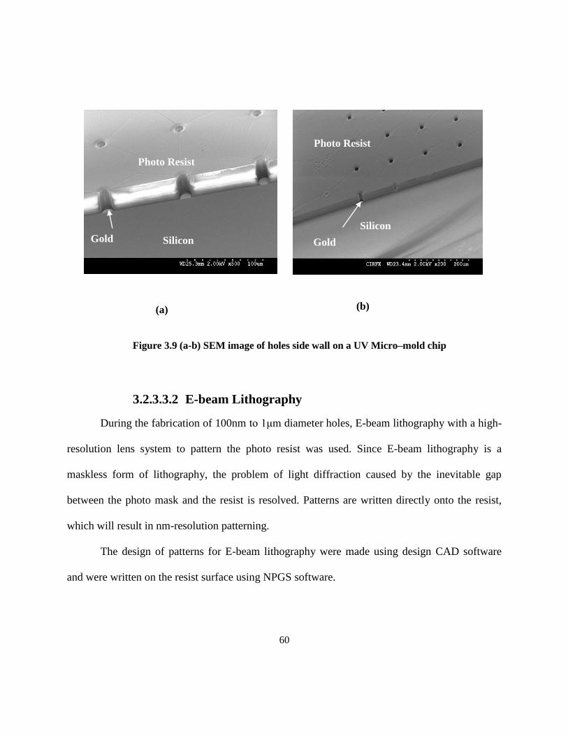
60
Figure 3.9 (a-b) SEM image of holes side wall on a UV Micro–mold chip
3.2.3.3.2 E-beam Lithography
During the fabrication of 100nm to 1μm diameter holes, E-beam lithography with a high-
resolution lens system to pattern the photo resist was used. Since E-beam lithography is a
maskless form of lithography, the problem of light diffraction caused by the inevitable gap
between the photo mask and the resist is resolved. Patterns are written directly onto the resist,
which will result in nm-resolution patterning.
The design of patterns for E-beam lithography were made using design CAD software
and were written on the resist surface using NPGS software.
Silicon
Gold
Photo Resist
Silicon
Photo Resist
Gold Silicon
Photo Resist
Gold
(a) (b)

61
To fabricate the E-beam samples, the fabrication process was divided into two steps: (A)
patterning the controlling surface, and (B) patterning the pillar growth section.
1. Patterning the Controlling Surface
As the controlling surface can be patterned easily via simple lithography procedure, the
E-beam micro-mold chips were first designed with controlling surfaces and were then processed
with E-beam writing. Here are the overall steps in patterning the controlling surface of E-beam
micro-mold chips:
1. Coat the gold chips with photo resist
2. Pattern the photo resist using photolithography through an emulsion photo mask
3. Develop the photo resist
4. Etch the gold/chromium
5. Strip the photo resist
Figure 3.10 shows these steps schematically.
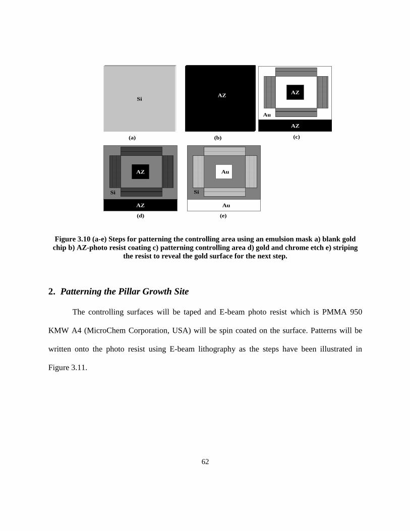
62
(a) (b)
Si
(e)
AZ
AZ
AZ
Au
AZ
AZ
Si
Au
AuAZ
AZ
Si
(c)
(d)
Figure 3.10 (a-e) Steps for patterning the controlling area using an emulsion mask a) blank gold
chip b) AZ-photo resist coating c) patterning controlling area d) gold and chrome etch e) striping
the resist to reveal the gold surface for the next step.
2. Patterning the Pillar Growth Site
The controlling surfaces will be taped and E-beam photo resist which is PMMA 950
KMW A4 (MicroChem Corporation, USA) will be spin coated on the surface. Patterns will be
written onto the photo resist using E-beam lithography as the steps have been illustrated in
Figure 3.11.

63
Figure 3.11 Schematic steps in fabrication of pillar growth site: a) tapping the controlling surface,
b) spin coating PMMA, c) writing the patterned area with E-beam
3.2.3.3.2.1 Emulsion Photo Mask
In order to pattern the controlling surface wafers, an emulsion mask was utilized instead
of a chromium mask since fabrication facilities were available on campus and because the array
pattern was large enough that the emulsion mask resolution provided good-quality patterning.
The original design of the mask was designed using the Corel Draw software and contained the
controlling surface with a diameter similar to those of the chromium mask, 0.4 x 10 mm. The
only difference was that the number of total arrays was sixty instead of fifty. Figure 3.12
illustrates a schematic of the emulsion mask.
AZ
AZ
Si
Au
Au
Tape
AZ
Si
Au
Tape
AZ
Si
Au
PMMA PMMA
(a) (b) (c)

64
Figure 3.12 Schematic of emulsion mask
The emulsion mask, an AGHD high-definition photo plate mask, with a high-contrast
silver halide, (Micro Chrome Technology, USA) was patterned using a 10x Mylar sheet. The
schematic design of the Mylar sheet is illustrated in Figure 3.13.
2.54 cm
10 mm 6 mm
# 60
2.54 cm
cninch

65
Figure 3.13 Schematic of mylar design
Emulsion Mask Fabrication
White light was exposed through the Mylar sheet in the UW dark room. A twelve second
exposure time was controlled by the equipment timer. Since the emulsion masks are highly-
sensitive to white light, it is important to ensure that there is no white light contamination during
the procedure. The procedure for fabricating the emulsion mask was as follows:
1. Place the Mylar sheet on the bottom holder.
25.4 cm
25.4 cm
100 mm
60 mm

66
2. Prepare the developing solution in 4:1 mixture of de-ionized water/developer solution
(640 ml DI water/160 ml developer)
3. Prepare the fixer solution in a 4:1 mixture of DI water/fixer (640 ml de-ionized water
/160 ml of fixer solution)
4. Ensure that there is no white light contamination and remove the emulsion mask
5. Place the emulsion mask in a photo mask holder
6. Expose to light for 12 seconds
7. Develop the mask for 3 minutes and 30 second with 5 seconds of dry time for every 25
seconds of developing
8. Rinse the mask with DI water for 3 minutes
9. Submerge the mask in the fixer solution for 3.5 minutes with 5 seconds of dry time for
every 25 seconds of fixing.
10. Rinsing the mask with DI water
Both the developer and fixer solutions are from Micro Chrome Technology, USA. Agitation was
applied during the developing and fixing process and the entire procedure was carried out at
room temperature.

67
3.2.3.3.2.2 Coating Gold Chips AZ Photo Resist
For patterning the controlling area with the emulsion mask, an AZ 3330 positive photo
resist (AZ Electronic Materials, USA) was dispensed onto chips using an Ultra 870series EFD
dispenser (Nordson Corporation, Canada). This resist is thermally stable up to 125ºC and coats
the surface smoothly. AZ photo resists are widely used in industry. The resist was spin coated in
a Model Ws-400A-6Npp/Lit spin coater (Laurell Technologies Corporation, USA) at 4000 rpm
for 45 seconds to take in 2.3μm thickness. The samples are then soft-baked at 90ºC for 5 minutes
on an EMS Precision Electronic Hot Plate Model 1000-1 (Electronic micro system ,UK)
followed by exposure through the emulsion photo mask to the UV light in the Oriel mask aligner
(Newport Corporation, USA) with a 500W unfiltered mercury lamp with a nominal 41 mW /cm2
power density.
The exposure time of twenty seconds, based on previous research experience in the lab,
was applied. The samples received post-exposure to improve the cross-linking reaction in the
photo resist, thus increasing its resistance to higher temperatures from reflowing. The optimum
post-exposure baking time for the samples was one minute at 110C.
An AZ 300 MIF developer (AZ Electronic Materials, USA) was used to develop the
resist. The developing time was found through a trial-and-error process. Although sixty seconds
of developing time is sufficient for a fresh developer solution, it was found that older developers
may require developing times up to ninety seconds.
The AZ photo resist in this step basically covers the gold surfaces on the controlling area
where the indium will be deposited on the gold surface of the pillar growth site (middle part),

68
and also the edge part of the chips where the alligator clip will conduct the electricity during the
plating procedure, as shown in Figure 3.14. The remaining chromium/gold surface was etched
away until the silicon substrate was revealed.
For etching the Cr/Au surface, chips are submerged in the gold etchant, type TFA
(Transene Company, USA), for ten seconds and then the wafer is submerged in the Chromium
Etchant Type 1020 (Transene Company, USA) for another 20-25 seconds. The native silicon
oxide will form on the silicon substrate at room temperature and will act as a resist for indium
deposition during the electro-deposition process. Having patterned the chip surface with AZ
photo resist, the chips are submerged in AZ-Stripper, Kwik stripper (AZ Electronic Materials,
USA) for at least fifteen minutes. The covered gold surface was then exposed for the next
process, as shown in Figure 3.14.
Gold GoldGold
Silicon
Figure 3.14 Schematic of categorized area using the UV lithography

69
The steps for patterning the controlling surfaces are as follows:
1. Place a needle on top of the AZ (3330) photo resist syringe and fill the needle with the
pedal of the resist dispenser to expel any bubbles.
2. Mount the wafer and the press vacuum in the spin coater.
3. Gently apply the resist to the wafers and close the lid.
4. Set the spin coater to 4000 rpm and spin coat the sample for 45 seconds at a 1215 rpm/sec
acceleration rate.
5. Bake the sample on the hotplate at 90°C for 5 minutes.
6. Change the mask aligner (holder) and/or the wafer holder, if necessary.
7. Mount the mask. Turn on the mask vacuum to hold it securely.
8. Align the sample and close the lid. Ensure that they are in good contact. Turn on the
chamber vacuum and place the sample under the shutter.
9. Set the timer to 20 seconds at 41mW2/m
2 intensity
10. Turn off the chamber vacuum
11. Bake the patterned samples on the hotplate at 110°C for 1 minute.
12. Use AZ MIF 300 developer to develop. Pour the developer into the labeled beaker and
prepare DI water. Place the samples into the developer for approximately 70-80 seconds
and then into DI water for 5-10 seconds. Wash them with DI water and dry them.
13. Check the samples under a microscope to verify whether or not the AZ has been fully
developed.
14. Place gold and chromium etchant into designated beakers and DI water into a DI water
beaker. Place the samples in the gold etchant for about 10 seconds, then into the DI water,
then the chromium etchant for 25 seconds and finally into the DI water.
15. Dry the samples and examine them under the microscope to ensure that the gold and
chromium have been fully etched away from the arrays.

70
16. Place the wafers in warm (60°C) Kwik stripper for ~15 minutes.
17. Wash the samples with DI water.
18. Blow dry the samples with nitrogen gas.
3.2.3.3.2.3 Oxygen Plasma Etch
After stripping the AZ photo resist from the surface, the wafers are oxygen plasma etched
to remove any possible AZ residue. A Trion Orion PECVD System (Trion Technology, USA)
was used with RIE power of 50 watts, ICP power of 50 watts, pressure of 20mtorr, oxygen flow
of 40 sccm, and RIE and ICP reflect of 4 watts. The detailed procedure for performing the
oxygen plasma etches with different conditions is discussed below
3.2.3.3.2.4 PMMA Photo Resist Coating
E-beam lithography was applied for higher-resolution patterning. Poly methyl
methacrylate (PMMA) 950 KMW A4 (MicroChem Corporation, USA) was applied as E-beam
resist. PMMA is a positive resist that contains a special poly methyl methacrylate grade to
provide high-contrast and high-resolution patterns in the processes [67]. Since fabrication
facilities for E-beam lithography were not available on campus, the chips were sent to the
University of Western Ontario to be processed there. The wafers were spin coated for 3 seconds
at 500 rpm and the speed was then ramped up to 1500 rpm and spun for an additional 1 minute.
The sample was then vacuum baked at 50C for 10min. The second layer of PMMA was spin
coated similarly. The thickness of the resist for creating 250 nm pillars is measured to be
750nm.

71
3.2.3.3.2.5 E-Beam Writing on PMMA
The pillar site was written on the resist using NPGS software and an appropriate E-beam
dosage. Pillar site design is illustrated in Figure 3.15, which shows that the total number of pillar
batches was 225, upon each of which 16 pillar growing sites were situated. Each of these batches
was identified by an address according to its location. The diameter corresponded with the pillar
diameters. The center-to-center distance of the cavities was 50 μm.
Figure 3.15 Schematic design of the pillar growth site
A range of E-beam dosages from 50% to 254% were applied in 0.9% increments of 500 μC /cm2.
Writing started at the (1,1) location with the lowest dose and followed a serpentine path to
(1,14), (1,15), (2,15), ( 2,14), (2,13), and so on. The size of the circular pattern was 250 nm, as
demonstrated in Figure 3.16.
#15
55
#X15 #Y01
#15
50 μm
50 μm
μm

72
50% of 500mC/cm²In
cres
cen
t of
0.9
%of
50
0m
C/c
m²
Dosage:
Dosage:
254% of 500mC/cm²
D=250nm
#X15#Y01
Figure 3.16 E-Beam write map with the applied dosage in each location.
Having the pattern written on the PMMA, the tapes were removed and the wafers were baked at
180C for 90 seconds.
3.2.3.3.2.6 Developing PMMA
PMMA was developed in three steps. While the wafers were spun at 500 rpm, the resist
was developed in a 1:3 mixture of methyl isobutyl ketone (MIBK) and isopropyl alcohol (IPA)
in an atomized spray developer for 90 seconds before being rinsed with IPA spray for sixty
seconds, and then blown dry with nitrogen gas.

73
PMMA
Gold
Silicon
Gold
Figure 3.17 Schematic of overall design of the E-beam micro – mold chip

74
(a) ( b)
Figure 3.18 (a-b) SEM image of processed E-Beam micro-mold chip: (a) Pillar growing site (b)
controlling surface
Figure 3.19 Schematic of the side wall mold design
PMMA Holes
Batch Address
Silicon
Gold

75
3.2.3.3.2.7 Oxygen Plasma Etching
The fabricated micro-mold chips were etched with oxygen plasma to ensure that the
PMMA residues were fully removed from the gold surface. It is important to use an appropriate
etching rate to ensure that the written photo resist is not etched in the process. By testing a range
of etching rates under different conditions, the best etching rate was calculated to be
approximately 100 nm /min. The samples were etched for fifteen seconds in 20 watt RIE and 0
watt ICP with 102 mtorr pressure and 40 sccm oxygen flows.
The steps of the etching process were as follows:
1. Prepare isopropyl alcohol and acetone in glass Petri dishes.
2. Use a cotton swab to clean the edge of the gold chip where it is patterned to control
the current. This is an important process to eliminate residues that were created from
tapes prior to spin coating.
3. First, apply acetone on a cotton swab and then carefully wipe one edge of the pattern.
Do this for the other three edges. Then use isopropyl alcohol to wipe the edges. This
process requires extreme caution because it is easy for either of the solutions to
contaminate the pillar growing site and remove the patterned PMMA.
4. Before placing the gold chip into the Trion Phantom Reactive Ion Etcher (RIE)
machine, the chamber must be cleaned with oxygen.
5. Click on “Cancel” when the screen is on “Stand By” mode.
6. Press the “Manual Process Control” button on the screen.
7. Turn the vacuum on. After 5 minutes, set the pressure to 20 m Torr RIE power to 50
watts, ICP power to 50 watts, and gas flow of oxygen to 40 sccm. Turn on the
pressure.
8. After 20 seconds, turn on the gas.
9. When the pressure and the gas flow are stabilized, turn on the plasma (RIE and ICP).

76
10. Use the knobs on the bottom of the machine to adjust RIE reflected power. Attempt
to reduce the reflected power to less than 10% of the applied power.
11. Adjust the ICP reflected power using the knobs on top of the machine. Also try to
make it less than 10% of the applied ICP power.
12. When the ICP and RIE powers are settled, increase the ICP power by 50 watts and
wait until it is settled. Increase it again by 50 watts to 200 watts.
13. Apply the mentioned conditions for about 300 seconds and then turn off the plasma.
Wait 30 seconds.
14. Turn off the gas. After 30 seconds, turn off the pressure.
15. The pressure to 102mtorr, ICP to 0watts, and RIE to 20 watts for a 100nm/min
etching rate.
16. Turn on the pressure and repeat steps 8 to 11. Leave it for 30 seconds.
17. Turn off the plasma and then the gas. Wait 30 seconds. Turn off pressure and
vacuum.
18. Exit from manual process control and click on “Vent Chamber.”
19. When the chamber lid opens, use a paper towel to clean the edge of the chamber.
Place the sample on the middle.
20. Press “Close Lid” on the screen.
21. Go to manual process control then turn on the vacuum and the pressure.
22. Repeat steps 8 and 9.
23. Ensure that the reflected RIE and ICP power are low and then apply 15 seconds for
etching.
24. Repeat steps 16 to 18 to turn off the machine.
25. When the chamber lid opens, carefully remove the sample.
26. Press “Close Lid” and then “Stand-by Mode” on the screen.
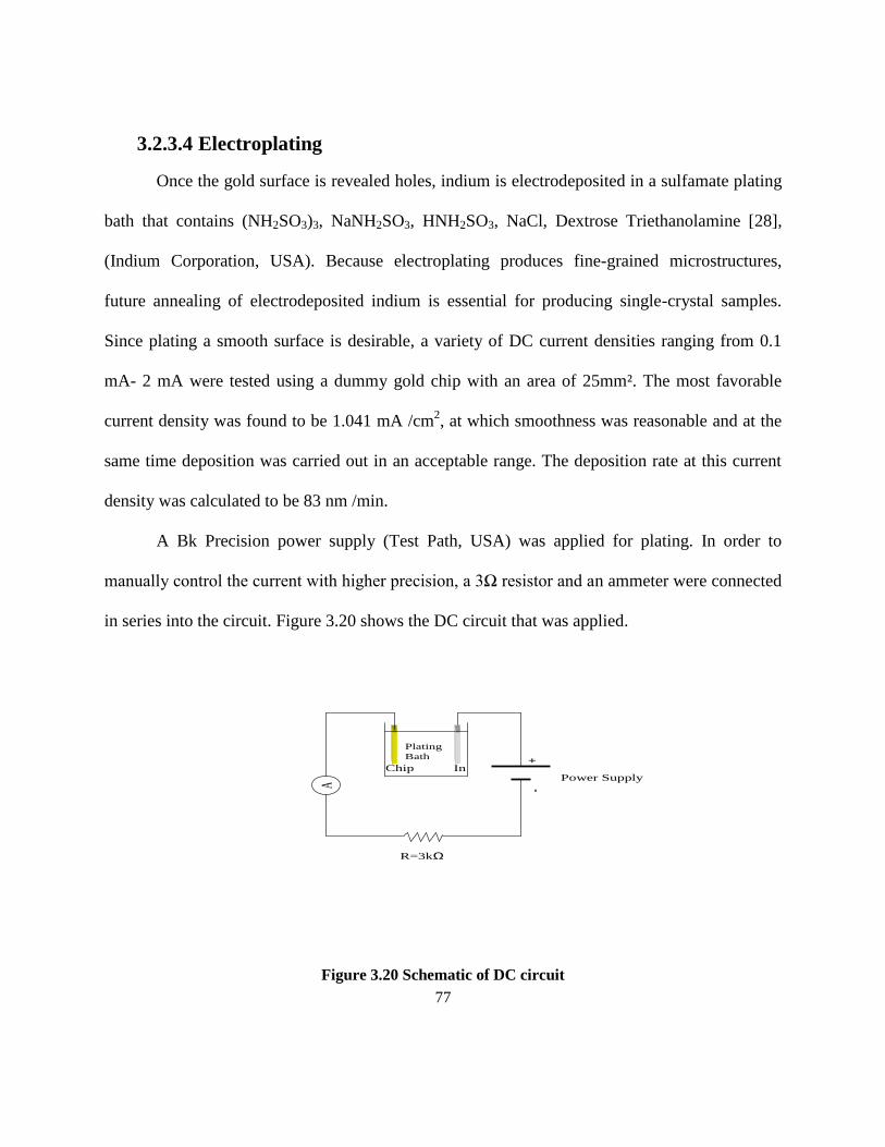
77
3.2.3.4 Electroplating
Once the gold surface is revealed holes, indium is electrodeposited in a sulfamate plating
bath that contains (NH2SO3)3, NaNH2SO3, HNH2SO3, NaCl, Dextrose Triethanolamine [28],
(Indium Corporation, USA). Because electroplating produces fine-grained microstructures,
future annealing of electrodeposited indium is essential for producing single-crystal samples.
Since plating a smooth surface is desirable, a variety of DC current densities ranging from 0.1
mA- 2 mA were tested using a dummy gold chip with an area of 25mm². The most favorable
current density was found to be 1.041 mA /cm2, at which smoothness was reasonable and at the
same time deposition was carried out in an acceptable range. The deposition rate at this current
density was calculated to be 83 nm /min.
A Bk Precision power supply (Test Path, USA) was applied for plating. In order to
manually control the current with higher precision, a 3Ω resistor and an ammeter were connected
in series into the circuit. Figure 3.20 shows the DC circuit that was applied.
R=3kΩ
Power Supply
-+
A
Plating
Bath
Chip In
Figure 3.20 Schematic of DC circuit

78
The anode is an indium bar sized 4 cm x 15 cm and the cathode is a micro-mold chip
sized 2.54 cm x 2.54 cm. The chip plating was carried out at room temperature according to the
following process:
1. Pour 200ml of indium plating solution into a 250 mL beaker and use a magnetic
stirrer to stir the bath at a constant speed.
2. Connect the gold chip as the cathode and indium bar as the anode.
3. To verify whether or not plating actually occurs and also if all of the connections are
stable, a current density of 1.041mA/cm2
is applied to a dummy gold chip for 2 to 3
minutes.
4. Connect an alligator clip to the bottom of the gold chip where the gold surface is
revealed. Place the gold chip into the solution and ensure that only the gold pad and
patterned edges are in the solution.
5. Use the sonication machine to insert the indium plating solution into the patterns.
This process is critical to ensure that plating occurs inside the pattern. Do this for at
least 3 minutes while also agitating the chip in the solution during sonication.
6. Connect the gold chip to the cathode side of the power supply and connect the indium
as the anode.
7. Apply the appropriate time of plating.
8. Turn off the DC power supply and magnetic stirrer. Pour de-ionized water into a Petri
dish and insert the gold chip sample for 5 minutes.
9. Remove and blow dry the sample.
10. Inspect the gold chip under a microscope to see if it is well-plated.

79
Figure 3.21 SEM image of one of the pillar site batches in E- beam micro-mold chip samples
3.2.3.5 Stripping Photo Resist
The photo resist will be stripped away from the surface after growing the indium pillar.
The total time taken for stripping the samples should be sufficient to fully remove the photo
resist; three days was found to be enough. A NanoTm
Remover PG (MicroChem Corporation,
USA) was used for stripping the SU-8 and a Kwik stripper (AZ Electronic Materials, USA), was
used for stripping the PMMA.
The steps for stripping the photo resist after plating are as follows:
Plated Indium
PMMA

80
Stripping the SU-8 from the UV-lithography samples:
1. Pour the PG remover solution into a beaker.
2. Place the UV-lithography-processed chip into a holder.
3. Heat the beaker to 60C in a sonicator.
4. Place the holder in the beaker.
5. Leave it for 48 hours.
6. Using extreme caution, remove the gold chip using tweezers. This must be done very
carefully since the pillars are very fragile and even a small amount of quick movement
can break them.
7. Pour isopropyl alcohol (99.7%) into a Petri dish and place the sample in very carefully.
Leave it in there for at least 5 minutes.
8. Remove the gold chip very carefully and use the Kim wipes to dry the edges of the gold
chips and let the gold pad where pillars are air dry.
Stripping PMMA from E-Beam lithography samples:
1. Pour the Kwik Strip solution into a Petri dish and insert the sample. Close the lid and
leave it for at least 48 hours.
2. Using extreme caution, remove the gold chip using tweezers. This must be done very
carefully because pillars are very fragile and even a little bit of quick movement can
break them.
3. Pour isopropyl alcohol (99.7%) into a Petri dish and insert the sample very carefully.
Leave it in there for at least 5 minutes.
4. Remove the chip very carefully and use the Kim wipe to dry the edges of the gold chips
and let the gold pad where pillars are air dry.

81
3.3 Some of the Fabricated Pillars
The following section lists some of the fabricated pillars with their corresponding plating
conditions.
Table 3.9 Plating condition for the UV-10μm micro-mold
Current
(mA)
Area
(mm2)
Voltage
(v)
Duration
(min)
Deposition rate
(nm/min)
Height
μm
0.5 44 1.56 240 83 20
Figure 3.22 SEM images of 10μm pillars
Indium pillar
Gold Gold
Indium pillar Indium pillar

82
Table 3.10 Plating condition of the E-Beam-500nm micro-mold
Figure 3.23 SEM image of plated pillar diameter 0.5 μm height of 1.5 μm
Figure 3.24 SEM image of the 0.5 μm plated indium. [10min deposition time was high so the over
plating indium forms these mushrooms
Current
(mA)
Area
(mm2)
Voltage
(v)
Duration
(min)
Deposition rate
(nm/min)
Height
μm
0.5 48 1.56 10 83 1.5
Gold
Indium
Gold
Indium
Gold
Indium

83
Table 3.11 Plating condition for E-Beam-250nm micro-mold
Current
(mA)
Area
(mm2)
Voltage
(V)
Duration
(min)
Deposition rate
(nm/min)
Height
(μm)
0.5 48 1.56 6.5 83 0.75
Figure 3.25 SEM image of 250 nm indium pillar
As can be seen in the Figure 3.25, the deposition duration was far higher than that
required, and the samples were over-deposited. On the other hand, giving a lower deposition
time prevented any plating from occurring on the chips. The application of a high current density
of 10.41 mA /cm² for 3.5 seconds improved indium pillar formation. The result of the applied
condition is illustrated in Figure 3.26.
D=281.1nm D=240.4nm
Indium Indium
D=258.6nm
Indium
Indium
Gold
n Gold

84
Table 3.12 Plating condition for E-beam-250 micro-mold
Figure 3.26 SEM images of 250nm fabricated pillars
Current
(mA)
Area
(mm2)
Voltage
(v)
Duration
(s)
Height
(μm)
1.5 48 4.52 3.5 -
0.5 48 1.5 510 0.75
95
254.nm
h=652nm
D=
Indium
Indium
Gold
Gold

85
Chapter 4
Result of Micro-Lithography Fabrication
4.1 Introduction
Two basic techniques for fabricating submicron-size indium pillars were discussed in the
previous chapter. The current chapter will present the scope of fabrication results and the effects
of various factors on process development. The best-known method of fabricating 250 nm pillar
samples will be presented also.
4.2 Effect of Ultraviolet Dosage
SU-8 is transparent photos resist which is not sensitive to UV light above 400 nm,
however, it absorbs wave lengths below 350 nm. Figure 4.1 shows the absorbance of different
SU-8 thicknesses ranging from 10-50 μm.
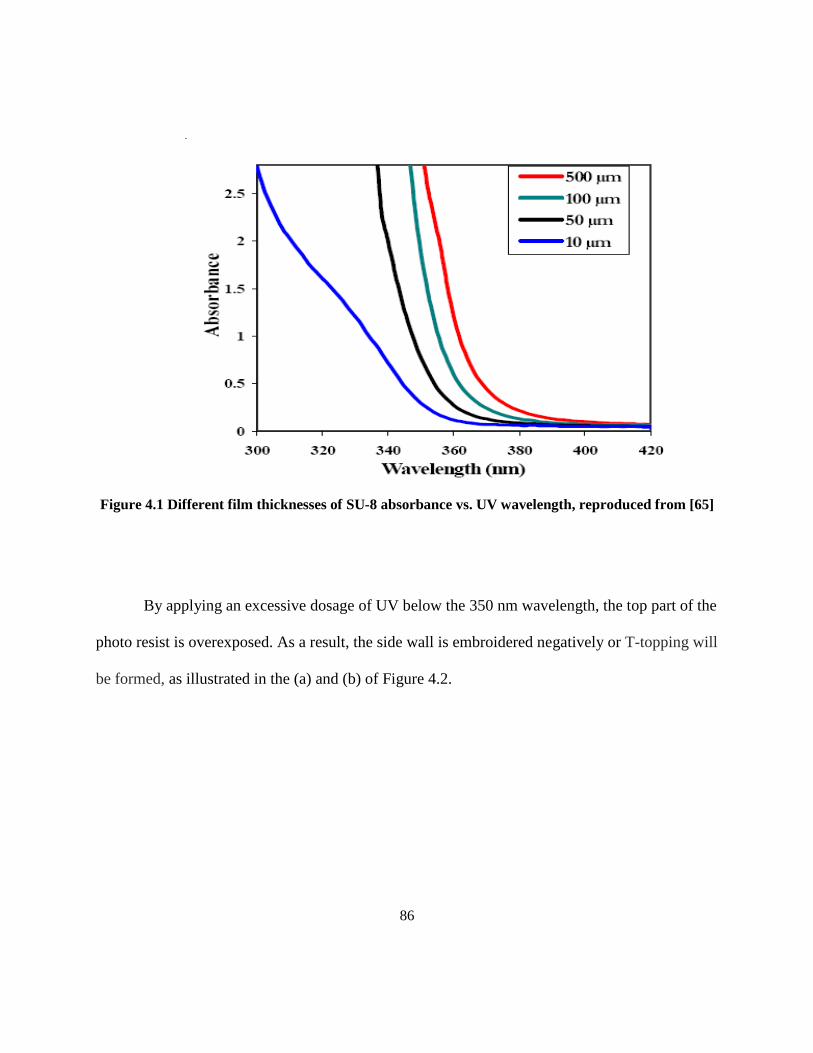
86
Figure 4.1 Different film thicknesses of SU-8 absorbance vs. UV wavelength, reproduced from [65]
By applying an excessive dosage of UV below the 350 nm wavelength, the top part of the
photo resist is overexposed. As a result, the side wall is embroidered negatively or T-topping will
be formed, as illustrated in the (a) and (b) of Figure 4.2.

87
Figure 4.2 ((a)-(d)) SEM image of fabricated mold (a) – (b) dosage 1000 mJ/cm2, (c)-(d) dosage
1800 mJ /cm2
By testing a range of dosages and exposure times as well as by using an i /liner filter
which filters out UV light below 360 nm, the T-topping was resolved as illustrated in the (c) and
(d) of Figure 4.2.
PHOTORESIST
GOLD
GOLD
Photo resist
GOLD
Silicon Silicon
Silicon Silicon
PHOTORESIST
Photo resist
(a) (c)
(d) (b)
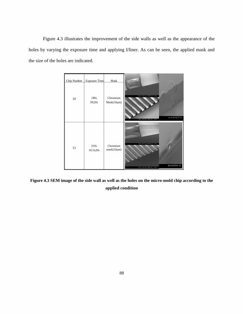
88
Figure 4.3 illustrates the improvement of the side walls as well as the appearance of the
holes by varying the exposure time and applying I/liner. As can be seen, the applied mask and
the size of the holes are indicated.
Chromium
Mask(10μm)
Chromium
mask(10μm)
180s
9X20s
210s
10.5x20s
10
11
MaskExposure TimeChip Number
Figure 4.3 SEM image of the side wall as well as the holes on the micro-mold chip according to the
applied condition
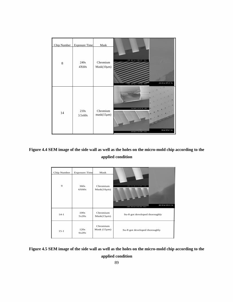
89
Chromium
Mask(10μm)
Chromium
mask(15μm)
240s
4X60s
210s
3.5x60s
8
14
MaskExposure Time Chip Number
Figure 4.4 SEM image of the side wall as well as the holes on the micro-mold chip according to the
applied condition
360s
6X60s
100s
5x20s
120s
6x20s
9 Chromium
Mask(10μm)
Chromium
Mask(15μm)
Chromium
Mask (15μm)
MaskExposure Time Chip Number
14-1
15-1
Su-8 got developed thoroughly
Su-8 got developed thoroughly
Figure 4.5 SEM image of the side wall as well as the holes on the micro-mold chip according to the
applied condition

90
The clean room’s alignment failed to operate during the development process and a new
aligner had to be used. This device was equipped with a set-up for dosage and so future
experiments were followed by varying dosages. A series of dosages from 1000 to 2000 mJ/cm2
were tested and the optimum dosage was found to be 1800 mJ /cm2.
4.3 Effect of Air Gap between the Photo Mask and Photo
Resist
As illustrated in Figure 4.6, the photo resist was bumped on top of the holes after being
developed in the developer during the initial attempts at the fabrication of micro-molds.
Figure 4.6 SEM image of developed 10 μm chip after post exposure bake
SILICON
SU-8 Photo resist
CR-Gold seed layer
LAYER
Photo Resist
Bump
PR

91
The appearance of bumpy surfaces can be explained by the inevitable air gap between the
photo mask and thick photo resists. The uneven thickness of the photo resist surface introduces
air gaps between the photo mask and resist, which result in pattern deformation. Thick photo
resists usually suffer from uneven thickness due either to beading at the border of the wafers
during spin coating or surface tension variation along the surface, which causes non-uniformity
during the soft bake process. The air gap causes Fresnel diffraction, which is the key
phenomenon in side wall enlarging during UV lithography printing [69]. The air gap causes the
angle of the exposed UV light to deviate to the unwanted area that was covered by a black
pattern on the photo mask, as illustrated in Figure 4.7, so some cross-linking reaction takes place
on these surfaces.
Dark pattern
Photo resist
Gap
White pattern
Exposed UV light
Figure 4.7 Schematic illustration of UV-light deviation due to the air gap

92
Some problems arise during the post-exposure bake since the exposed and unexposed
areas have different thermal expansion coefficients; the area with the higher expansion
coefficient will expand more in correspondence with the deeper unexposed photo resist during
the post-exposure bake and the photo resist will take on a bumpy-shaped form. The exposed and
unexposed parts are shown in Figure 4.8.
Exposed area
Unexposed area
Photo resist
Figure 4.8 Schematic illustration of photo resist exposed and unexposed area under photo-mask
black patterns
As illustrated in Figure 4.9, reducing the air gap between the photo mask and the resist
will cause the intensity distribution of the Fresnel diffraction to get closer to the intensity

93
distribution of the perfect contact. This will directly improve the UV light exposure process and
the straightness of the side walls [69]. L
fx/l
inc
Position (m)
Slit width 15um
With 100 um air gap
----------- Slit width 15um
With 30um air gap
Figure 4.9 Intensity distribution of Fresnel diffraction for different air gap thickness: L fx Fresnel
diffraction intensity, L inc intensity of incident vs. the photo mask distance from photo resist surface,
reproduced from [69]
To reduce the gap between the resist and the photo mask, the gap was filled with a
glycerol (C3H8O3). As glycerol has a reflection index of 1.4729 at 20°C, which is close to the
mask glass reflection index of 1.474 at 20°C, it will fill the air gap and improve side wall
patterning. Figure 4.10 shows that the Fresnel diffraction has improved by injecting the glycerol
into the gap.
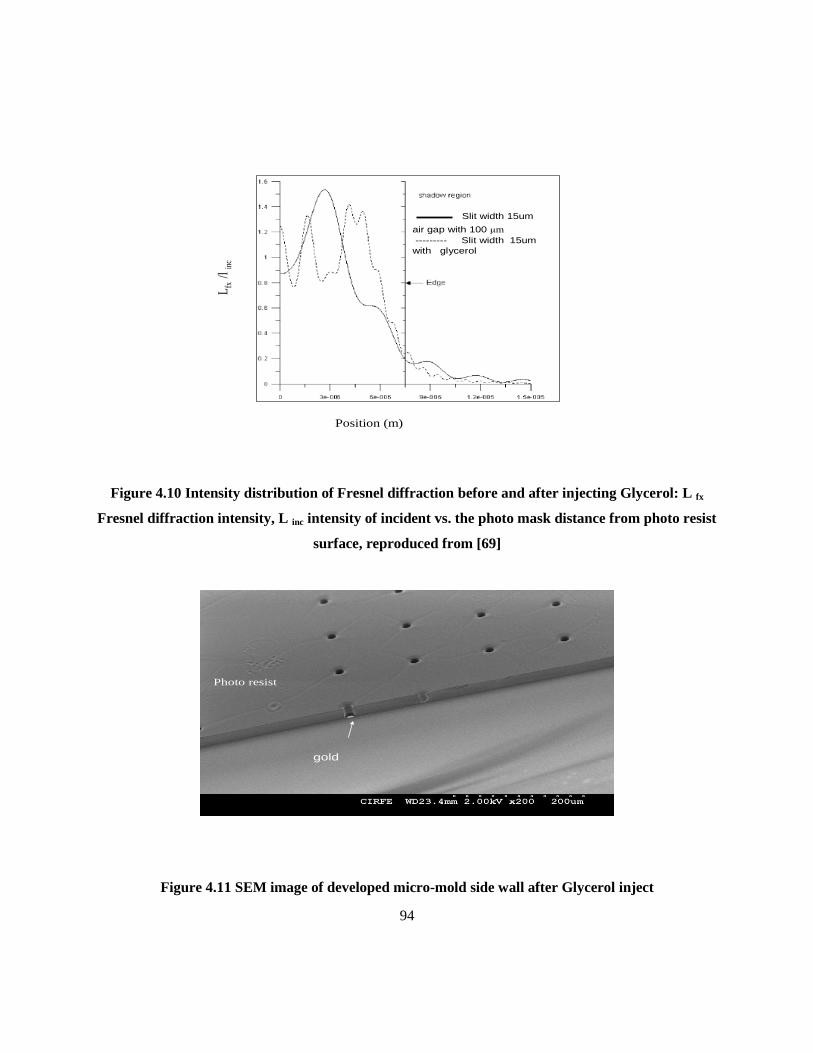
94
Lfx
/l in
c
Position (m)
Slit width 15um
air gap with 100 μm
--------- Slit width 15um
with glycerol
Figure 4.10 Intensity distribution of Fresnel diffraction before and after injecting Glycerol: L fx
Fresnel diffraction intensity, L inc intensity of incident vs. the photo mask distance from photo resist
surface, reproduced from [69]
gold
Photo resist
Figure 4.11 SEM image of developed micro-mold side wall after Glycerol inject

95
Chromium
Mask(10μm)
Chromium
mask(10μm)
1200
1400
23
24
MaskDosage mJ/cm2
Chip
Number
Figure 4.12 SEM image of micro-mold side wall corresponding to the applied condition, before
Glycerol inject
Chromium
Mask(10μm)
Chromium
mask(10μm)
1400
1800
28
30
MaskDosage
mJ/cm2
Chip
Number
30
Figure 4.13 SEM image of micro-mold side wall corresponding to the applied condition, after
Glycerol inject

96
4.4 Pulse Plating
Pulse plating experiments were conducted during the plating process. As indicated in
many experiments [55-59], the morphology of the deposited material can be improved by using
pulse plating. Pulse plating improves mass transport, which has an important influence on
deposition rate and deposition properties. By applying the pulses during pulse plating, the ion
concentration in the solution is controlled more efficiently than in DC plating. During the period
in which the cathode current is applied, the reactant ions are plated onto the cathode due to the
reduction reaction. During the off period, or anodic current, the plated ion species are refilled
either by the transport phenomena that convey more ions from the bulk solution or by dissolution
of the dendrites which have low stability in the solution [68].
The Potentiostat model EPP4000 (Princeton applied research, USA) was used. In
conventional DC plating, only current density is a changeable variable, while in pulse plating at
least three different parameters, such as the on-time, off-time, and peak current density, can be
changed.
There are basically two types of wave form that have been tested by potentiostat. The
first approach was to give a negative and positive pulse and the second was to just give a peak
pulse in order to nucleate the deposition followed by application of a constant current.
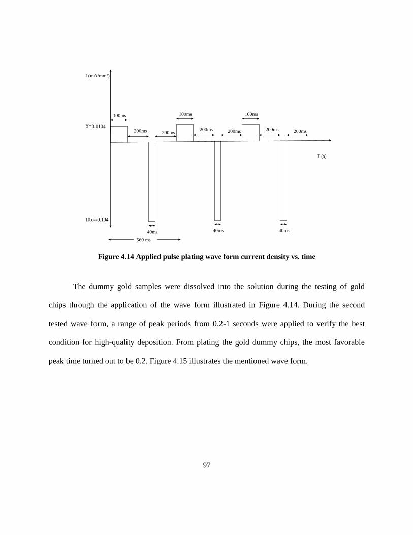
97
100ms
200ms
40ms
200ms
100ms
200ms
40ms
200ms
100ms
200ms
40ms
200ms
T (s)
I (mA/mm2)
X=0.0104
560 ms
10x=-0.104
Figure 4.14 Applied pulse plating wave form current density vs. time
The dummy gold samples were dissolved into the solution during the testing of gold
chips through the application of the wave form illustrated in Figure 4.14. During the second
tested wave form, a range of peak periods from 0.2-1 seconds were applied to verify the best
condition for high-quality deposition. From plating the gold dummy chips, the most favorable
peak time turned out to be 0.2. Figure 4.15 illustrates the mentioned wave form.

98
Figure 4.15 Favored wave form for plating the micro-mold chips using potentiostat current density
vs. time
10x=0.104
x=0.0104
0.2s 600s
i (mA/mm2)
t (s)

99
Figure 4.16 SEM image of plated 250 nm micro-mold chip using potentiostat by applying 0.2 second
10.4 mA /cm² and 10 min of 1.04 mA/ cm² current density.
As shown in Figure 4.16, using the potentiostat did not improve the formation of the
indium pillars; thus, conventional DC plating was used again. A current density of 10.04 mA/cm²
was applied for 3.5 seconds in order to achieve deposition nucleation, as illustrated in Figure
4.16. Applying this wave form has improved the formation of the pillars, as demonstrated in
Figure 4.17.
Indium pillar
Gold
Indium pillar
Gold
D=804.9nm
D=770.0nm
Indium
Gold Gold Indium

100
Figure 4.17 The applied wave form using Dc Power supply, current density mA /mm² vs. time(s).
10x=0.104
x=0.0104
3.5s 600s
i (mA/mm2)
t (s)
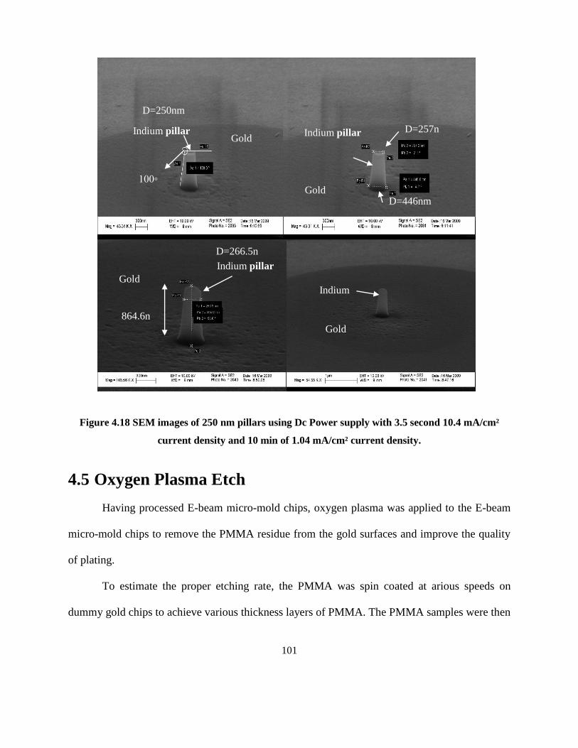
101
Figure 4.18 SEM images of 250 nm pillars using Dc Power supply with 3.5 second 10.4 mA/cm²
current density and 10 min of 1.04 mA/cm² current density.
4.5 Oxygen Plasma Etch
Having processed E-beam micro-mold chips, oxygen plasma was applied to the E-beam
micro-mold chips to remove the PMMA residue from the gold surfaces and improve the quality
of plating.
To estimate the proper etching rate, the PMMA was spin coated at arious speeds on
dummy gold chips to achieve various thickness layers of PMMA. The PMMA samples were then
Indium pillar Gold
D=250nm
100
Indium pillar
Gold
D n
Gold
Gold
Indium
pillar
Indium pillar
D=257n
m
D=446nm
D=266.5n
m
864.6n
m

102
etched by applying oxygen plasma with different amount of RIE, an ICP, and pressure.
Correspondingly, the condition that supplied an appropriate etching was chosen. Table 4.1
illustrates the applied condition and resultant etch rate of PMMA. The favored condition was
applying 20 watts, RIE 0 watts, ICP and 102mtorr of pressure, and 40 sccm oxygen flow.
Under the aforementioned conditions, an etching rate of 1.6667 nm /sec was calculated to
be reasonable for etching. The total applied time for etching was 15 seconds for 250 nm-E-beam
micro-molds.
Table 4.1 PMMA etching rates corresponding to the applied
etching condition, units of pressure is mTorr, RIE power is Watt, ICP Power is Watt and oxygen
flow is sccm.
Set
Pressure
Pressure
Read
RIE
Power
RIE
Read
RIE
Ref
ICP
Power
ICP
Read
ICP
Ref
Oxygen
Flow
Oxygen
Read
Rate
(nm/s)
22 19~20 50 52 2 0 1 2 40 39 5.988456
22 19~20 25 26~27 3 25 26~27 2 40 39 5.3663
22 19~20 10 10 3 20 21~22 2~3 40 39 1.95448
22 19~20 20 22 2 0 1 2 40 39 1.6667
102 99~100 50 52 4 0 1 2 40 39 6.61187
102 99~100 20 22 1 0 2 1~2 40 39 1.6667

103
Figure 4.19 SEM images of 250 nm pillars using Dc Power supply with 3.5 second 10.4 mA/cm²
current density and 10 min of 1.04 mA /cm² current density and oxygen plasma etch
95
254.nm
h=652n
m
D=
Indium
Indium
Gold
Gold

104
Chapter 5
Summary
In the present research, a process was developed for fabricating submicron-scale indium
samples for use in compression tests. The FIB was used during the process to mill the pillar
samples to the desired diameter. However, the low melting point of indium limited its application
for fabricating the sub-micron pillars. As a result, an alternative technique known as micro-
lithography was used for fabrication. As the fabrication of finer-diameter pillars required a
higher resolution patterning, E-beam lithography was employed. Versatile micro fabrication
techniques were applied during the micro-mold fabrication process in order to improve the
quality of features such as side wall straightness and smoothness. Pulse plating was applied for
growing indium pillars; however, the result was not favorable over DC plating. The pillar was
characterized by SEM and it can be seen that fabricated pillars satisfy the criteria of performing
the compression test.

105
5.1 Recommendations
The following recommendations are made for future work:
1. Developing the E-beam lithography techniques to fabricate sub-100 nm diameter indium
pillars.
2. Manufacture different grain sizes pillar samples by annealing them or improving the
plating process to grow finer grains.
3. Test the creep relaxation behaviours of sub-micron pillars using the compression test to
verify if the indium mechanical behavior deviates from the bulk.
4. Depositing other materials, such as cobalt and nickel, in the micro-mold chips via
electroplating to create sub-micron pillar samples for compression test.

106
REFERENCES
[1] Dieter, G. E. 1988. Mechanical metallurgy. 6th ed. New York: McGraw-Hill.
[2] Courtney, Thomas H. 1990. Mechanical behavior of materials. New York; Montreal:
McGraw-Hill.
[3] Shackelford, James F. 2005. Introduction to materials science for engineers. 6th ed. Upper
Saddle River, NJ: Pearson Education Inc.
[4] Nix, William D., and Huajian Gao. 1998. Indentation size effects in crystalline materials: A
law for strain gradient plasticity. Journal of the Mechanics and Physics of Solids 46, (3) (3): 411-
25.
[5] Ma, Q., Clarke. D.R., 1995. Size-Dependent Hardness Of Silver Single-Crystals. Journal Of.
Materials Research, 10 (4), 853-863
[6] Poole, W. J., M. F. Ashby, and N. A. Fleck. 1996. Micro-hardness of annealed and work-
hardened copper polycrystals. Scripta Materialia 34, (4, pp. 559-564): February.
[7] Gerberich, W. W., N. I. Tymiak, J. C. Grunlan, M. F. Horstemeyer, and M. I. Baskes. 2002.
Interpretations of indentation size effects. Journal of Applied Mechanics 69, (4): 433 (10) - 443.
[8] Atkinson, M. 1995. Further analysis of the size effect in indentation hardness tests of some
metals. Journal of Materials Research 10, (11) (11): 2908-15.
[9] Penn state Innovation Report: “Tiny Tools Carve Glass.” Report 2004; 35711.

107
[10] Fleck, N. A., G. M. Muller, M. F. Ashby, and J. W. Hutchinson. 1994. Strain gradient
plasticity: Theory and experiment. Acta Metallurgica Et Materialia 42, (2) (02): 475-87.
[11] Voskerician, Gabriela(1), Matthew S. (1) Shive, Rebecca S. (2) Shawgo, Horst von(3)
Recum, James M. (1) Anderson, Michael J. (2) Cima, and Robert(4) Langer. 2003.
Biocompatibility and biofouling of MEMS drug delivery devices. Biomaterials 24, (11): 1959-
67.
[12] McAllister, D. V., M. G. Allen, and M. R. Prausnitz. 2000. Microfabricated microneedles
for gene and drug delivery. Annual Review of Biomedical Engineering 2, : 289-313.
[13] Huynh, Wendy U., Janke J. Dittmer, and A. Paul Alivisatos. 2002. Hybrid nanorod-polymer solar
cells. Science 295, (5564) (March 29): 2425-7.
[14] Tabor, D. 1951. The hardness of metals. Oxford, London; UK: Clarendon Press.
[15] Pethica, J. B., R. Hutchings, and W. C. Oliver. 1983. Hardness measurement at penetration
depths as small as 20 nm. Philosophical Magazine A: Physics of Condensed Matter 48, (4): 593-
606.
[16] Doucet, L., and G. Carlotti. 1995. Elastic properties of silicate glass and spin-on glass thin
films. Paper presented at Proceedings of the 1994 MRS Fall Meeting, start date 19941128-
enddate 19941201.
[17] Atkins, A. G., A. Silvero, and D. Tabor. 1966. Indentation hardness and the creep of solids.
Inst Metals J 94, (1) (Nov.): 369-78.
[18] Mayo, M. J., and W. D. Nix. 1988. A micro-indentation study of super plasticity in Pb, Sn,
and Sn-38 wt% pb. Acta Metallurgica 36, (8, pp. 2183-2192): August.

108
[19] Lucas, B. N., W. C. Oliver, G. M. Pharr, and J. -L Loubet. 1996. Time dependent
deformation during indentation testing. Paper presented at Materials Research Society
Symposium - Proceedings, vol. 436, 1996; Proceedings of the 1996 MRS Spring Meeting, start
date 19960408-enddate 19960412.
[20] Baker, S. P., W. D. Nix, and T. W. Jr Barbee. 1992. Time-dependent deformation in room-
temperature indentation experiments using a nanoindenter. Paper presented at Thin Films:
Stresses and Mechanical Properties. III; Boston, Massachusetts; USA; 2-5 Dec. 1991; Thin
Films: Stresses and Mechanical Properties. III, Boston, Massachusetts; USA.
[21] Yoder, K. B., D. S. Stone, J. C. Lin, and R. A. Hoffman. 1995. Indentation creep of
molybdenum: Comparison between thin film and bulk material. Paper presented at Thin Films:
Stresses and Mechanical Properties V; Boston, MA; USA; 28 Nov.-2 Dec. 1994; Thin Films:
Stresses and Mechanical Properties V, Boston, MA; USA.
[22] Chu, S .N. G and Li, J .C .M .1977. Impression creep, new creep tests J. Mater. Sci. 12
2200–8.
[23] Chu, S. N. G., and J. C. M. Li. 1979. Impression creep of β-tin single crystals. Materials
Science and Engineering 39, (1, pp. 1-10): July.
[24] Feng, G., and A. H. W. Ngan. 2001. Creep and strain burst in indium and aluminum during
nanoindentation. Scripta Materialia 45, (8, pp. 971-976): October.
[25] Lucas, B. N., and W. C. Oliver. 1995. Time dependent indentation testing at non-ambient
temperatures utilizing the high temperature mechanical properties microprobe. Paper presented
at Proceedings of the 1994 MRS Fall Meeting, start date 19941128-enddate 19941201.

109
[26] Syed Asif, S. A., and J. B. Pethica. 1997. Nanoindentation creep of single-crystal tungsten
and gallium arsenide. Philosophical Magazine A (Physics of Condensed Matter: Structure 76, (6)
(12): 1105-18.
[27] Alfantazi, A. M., and R. R. Moskalyk. 2003. Processing of indium: A review. Minerals
Engineering 16, (8): 687-94.
[28] Indium Corporation, solder and solder paste. Retrieved Feb 20, 2008, from Web site:
http://www.indium.com/
[29] Swadener, J.G., E.P. George, and G.M. Pharr, 2002. The correlation of the indentation size
effect measured with indenters of various shapes. Journal of the Mechanics and Physics of
Solids, 50:681:694.
[30] Ashby, M. F. (1). 1970. The deformation of plastically non-homogeneous materials.
Philosophical Magazine 21, (170) (02): 399-424.
[31] Page, T. F., W. C. Oliver, and C. J. McHargue. 1992. The deformation behavior of ceramic
crystals subjected to very low load (nano) indentations. Journal of Materials Research 7, (2)
(02): 450-73.
[32] Gerberich, W. W., N. I. Tymiak, J. C. Grunlan, M. F. Horstemeyer, and M. I. Baskes. 2002.
Interpretations of indentation size effects. Journal of Applied Mechanics 69, (4): 433(10) - 443.
[33] Mann, A. B., and J. B. Pethica. 1996. Dislocation nucleation and multiplication during
nanoindentation testing. Paper presented at Materials Research Society Symposium-
Proceedings, vol. 436, 1996; Proceedings of the 1996 MRS Spring Meeting, start date 19960408-
enddate 19960412.

110
[34] Corcoran, S. G. (1), R. J. (1) Colton, E. T. Lilleodden, and W. W. Gerberich. 1997.
Anomalous plastic deformation at surfaces: Nanoindentation of gold single crystals. Physical
Review B (Condensed Matter) 55, (24) (06): R16057-60.
[35] Jarausch, K. F., J. D. Kiely, J. E. Houston, and P. E. Russell. 2000. Defect-dependent
elasticity: Nanoindentation as a probe of stress state. Journal of Materials Research 15, (8):
1693-701.
[36] Suresh, S., T. G. Nieh, and B. W. Choi -. 1999. Nano-indentation of copper thin films on
silicon substrates. Scripta Materialia (USA) 41, (9) (8 Oct.): 951-7.
[37] Van der Merwe, J. H., and F. C. Frank. 1949. Misfitting monolayers. Proceedings of the
Physical Society. Section A 62, (May): 315-6.
[38] Matthews, J. W. (1), and A. E. (1) Blakeslee. 1975. Defects in epitaxial multilayers: II.
Dislocation pile-ups, threading dislocations, slip lines and cracks. Journal of Crystal Growth 29,
(3): 273-80.
[39] Matthews, J. W., and A. E. Blakeslee. 1974. Defects in epitaxial multilayers. Journal of
Crystal Growth 27: 118-25.
[40] Freund, L. B. (1). 1987. The stability of a dislocation threading a strained layer on a
substrate. Transactions of the ASME. Journal of Applied Mechanics 54, (3) (09): 553-7.
[41] Nix, W. D. 1998. Yielding and strain hardening of thin metal films on substrates. Paper
presented at Scripta Materialia, vol.39, no.4-5, pp.545-554, 4 Aug. 1998; Defects in Crystals: A
Symposium Honoring the Contributions of John P Hirth. Held at the TMS Annual Meeting,
16-19 Feb. 1998, San Antonio, TX, USA. TMS,

111
[42] Greer, J. R. (1), and W. D. (1) Nix. 2005. Size dependence of mechanical properties of gold
at the sub-micron scale. Applied Physics A (Materials Science Processing) A80, (8) (05): 1625
[43] Greer, J. R., W. C. Oliver, and W. D. Nix. 2005. Size dependence of mechanical properties of gold
at the micron scale in the absence of strain gradients. Acta Materialia 53, (6): 1821-30.
[44] Greer, J. R., W. C. Oliver, and W. D. Nix. 2006. Corrigendum to "size dependence in
mechanical properties of gold at the micron scale in the absence of strain gradients" [acta mater
53 (6) (2005) 1821-1830]. Acta Materialia 54, (6) (Apr): 1705.
[45] Greer, J. R. (1), and W. D. (1) Nix. 2006. Nanoscale gold pillars strengthened through
dislocation starvation. Physical Review B (Condensed Matter and Materials Physics) 73, (24)
(06): 245410, 2451-6.
[46] Uchic, M. D. (1), D. M. (1) Dimiduk, J. N. Florando, and W. D. Nix. 2004. Sample
dimensions influence strength and crystal plasticity. Science 305, (5686) (08): 986-9.
[47] Uchic, M. D. (1), and D. M. (1) Dimiduk. 2005. A methodology to investigate size scale
effects in crystalline plasticity using uniaxial compression testing. Materials Science &
Engineering A (Structural Materials: Properties 400-401, (07): 268-78.
[48] Dimiduk, D. M., M. D. Uchic, and T. A. Parthasarathy. 2005. Size-affected single-slip
behavior of pure nickel microcrystals. Acta Materialia 53, (15) (09): 4065-77.
[49] Dimiduk, D. M., C. Woodward, R. Lesar, and M. D. Uchic. 2006. Scale-free intermittent
flow in crystal plasticity. Science 312, (5777) (05): 1188-90.
[50] Volkert, C. A., and E. T. Lilleodden. 2006. Size effects in the deformation of sub-micron au
columns. Philosophical Magazine 86, (33-35) (11): 5567-79.
112
[51] Brinckmann, S., Ju-Young Kim, and J. R. Greer. 2008. Fundamental differences in
mechanical behavior between two types of crystals at the nano scale. Physical Review Letters
100, (15) (04): 155502, 1551-4.
[52] Shan, Z. W., J. Li, Y. Q. Cheng, A. M. Minor, S. A. S. Asif, O. L. Warren, and E. Ma. 2008.
Plastic flow and failure resistance of metallic glass: Insight from in situ compression of
nanopillars.
[53] Van Der Biest, O., and J. Van Der Planken. 1973. The plastic deformation of indium single
crystals. Acta Metallurgica 21, (12, pp. 1629-1639): December..
[54] Giannuzzi, L. A. and Stevie, F. A.2005, “Introduction to Focused Ion Beams:
Instrumentation, Theory, Techniques and Practice”, Springer, New York.
[55] Andricacos, P. C., and M. Datta. 1987. [Theory and practice of pulse plating (book review)].
Plating and Surface Finishing 74, (March): 80-1.
[56] Tang, Peter Torben, Henrik Dylmer, and Per Mo slashedller. Electroplating method of
forming platings of nickel. Patent USA 6036833.
[57] Jernstedt, G. W. 1947. PR plating, a new tool for electroplaters. Westinghouse Engineer 7,
(May): 89-92.
[58] Sverdlov, Y., Y. Rosenberg, Y. I. Rozenberg, R. Zmood, R. Erlich, S. Natan, and Y.
Shacham-Diamand. 2004. The electrodeposition of cobalt-nickel-iron high aspect ratio thick film
structures for magnetic MEMS applications. Microelectronic Engineering 76, (1-4): 258-65.

113
[59] Gomez, E., E. Pellicer, and E. Valles. 2005. Electrodeposition of cobalt based alloys for
MEMS applications. Transactions of the Institute of Metal Finishing 83, (5): 248-54.
[60] Gomez, E., E. Pellicer, and E. Valles. 2005. Electrodeposition of cobalt based alloys for
MEMS applications. Transactions of the Institute of Metal Finishing 83, (5): 248-54
[61] Brener, A. 1965. Electrodeposition of alloys, past, present, and future. Plating 52, (12)
(Dec.): 1249-57.
[62] Bard.A.J., and Faulkner.L.R. 2001. Electrochemical Methods: Fundamentals and
Applications. 2nd ed., John Wiley & Sons, New York.
[63] Kim, J., H. Schoeller, J. Cho, and S. Park. 2008. Effect of oxidation on indium solders
ability.
[64] Kern, W., and Puotinen D. A. 1970. Cleaning solutions based on hydrogen peroxide for use
in silicon semiconductor technology, RCA Review, vol. 31, 187.
[65] MicroChem Corpotation,. Data sheet SU-8 2-25. Retrieved May 20, 2008, from
Photoresistes formulations SU-8 2-25
Website:http://mems.gatech.edu/msmawebsite/members/processes/processes_files/SU8/Data%2
0Sheet%202-25.pdf
[66] MicroChem Corporation, SU-8-material data sheet. Retrieved July 6, 2008, from Material
Saftey Data Sheet Web site: http://www.bioeng.nus.edu.sg/biofluids/intranet/MSDS/su-8-dev.pdf
[67] MicroChem Corporation, Newton, Ma, PMMA product information sheet. Retrieved Sep,
2008, from PMMA &Copolymer Web site: “PMMA product information sheet “MicroChem

114
Corporation, Newton, Ma, [online]
Available:http://www.microchem.com/products/pdf/PMMA_Data_Sheet.pdf.
[68] Popov, K. I., M. D. Maksimović, B. M. Ocokoljić, and B. J. Lazarević. 1980. Fundamental
aspects of pulsating current metal electrodeposition I: The effect of the pulsating current on the
surface roughness and the porosity of metal deposits. Surface Technology 11, (2): 99-109.
[69] Chuang, Y. J, F.G Tseng, and W. -K Lin. 2002. Reduction of diffraction effect of UV
exposure on SU-8 negative thick photoresist by air gap elimination. Microsystem Technologies 8,
(4-5): 308-13.

115
Appendix A
Best Known Method for Fabricating 0.25μm Pillars

116
1. Cleaning Silicon wafers (Section3.2.3.1, Page 46)
Dice the samples to 2.54 x 2.54 cm
Solution: 5:1:1H2O/H2O2/NH4OH solution at 75ºC
Time: submerge the wafers for 15 minutes
Solution: 700ml of DI water at 80-90 ºC hot water
Time: submerge the wafer for 15 minutes in hot water
Wash the wafer under running DI water and dry with nitrogen gas
2. Cr/Au Deposition (Section3.2.3.2, Page 47)
Instrument: Nanochrome TM
DC sputtering system (Intelvac, Canada)
Vacuum chamber for 45 minutes to reach 3.26E-6 Torr pressure
Chamber temperature: 10.9K
Set chromium thickness: 40nm
Set gold thickness: 60nm
3. AZ Photo Resist Coating (Section 3.2.3.3.2.2, Page 67)
Photo resist type: AZ 3330 positive photo resist, ( AZ Electronic Materials, USA)
Instrument: Ws-400A-6Npp/Lit Spin coater (Laurell Technologies Corporation,
USA)
Spin speed: 4000 rpm
Acceleration rate: 1215 ramp/sec
Time: 45 seconds
Soft-baked at 90ºC for 5 minutes on EMS Precision Electronic Hot Plate

117
4. Patterning with Emulsion Mask (Section 3.2.3.3.2.2, Page 70)
Instrument: Oriel mask aligner (Newport Corporation, USA)
Power density: 41mW/Cm²
Expose time: 20 second
Post exposure bake at 110C for 1 min on EMS Precision Electronic Hot Plate
5. Developing AZ–Photo Resist (Section 3.2.3.3.2.2, Page 70)
Developer: AZ MIF 300 developer ( AZ Electronic Materials, USA)
Developing time 80-90 seconds
Submerge in DI water for 5-10 seconds
6. Gold Etch (Section 3.2.3.3.2.2, Page 70)
Etchant: Gold etchant type TFA (Transene Company, USA)
Time: ~10 second.
Temperature: room temperature
Submerge in DI water for 5-10 seconds
7. Chromium Etch (Section 3.2.3.3.2.2, Page 70)
Chromium Etchant Type 1020 (Transene Company, USA)
Time:~ 20-25 seconds
Temperature: room temperature
Submerge in DI water for 5-10 seconds

118
8. Stripping AZ resist (Section 3.2.3.3.2.2, Page 70)
AZ stripper: Kwik stripper (AZ Electronic Materials, USA)
Time: ~15 minutes
Temperature: 60°C
DI water washing / nitrogen blow drying
9. Oxygen Plasma Etch the Wafers (Section 3.2.3.3.2.3, Page 70)
Instrument: Trion Orion Plasma-Enhance Chemical Vapor Deposition (PECVD)
System (Trion Technology, USA)
Conditions:
Table 5.1 Oxygen etch condition for removing AZ residues
Time: 3 minutes
Tape the controlling area surface
10. PMMA Coating (Section 3.2.3.3.2.3, Page 70)
Photo resists: Poly methyl methacrylate (PMMA) 950KMW A4 (MicroChem
Corporation, USA)
Spin coating the second layer of PMMA, Speed: 500rpm for 3 seconds, speed ramp to
1500 rpm and hold for 1 minute
Set
P
(mT)
Read
P(mT)
RIE
(W)
RIE
Read(w)
RIE
Ref
ICP
(W)
ICP
Read(w)
ICP
Ref
Oxygen
Flow(sccm)
20 19~20 50 52 4 50 52 4 40

119
Soft bake at 50C for 10 minutes on vacuum hotplate
Spin coating second layer of PMMA, Speed: 500 rpm for 3 seconds, speed ramp to
1500 rpm and hold for 1 minute
Soft bake at 50C for 10 minutes on vacuum hotplate
PMMA Thickness: 750nm
11. E-Beam Lithography (Section 3.2.3.3.2.4, Page 71)
Applied dosage for fabricating the 250 nm pillar site in 15 x15 regions, was 50%-
254% of 500 mC /cm² with increment of 0.9% in the serpentine pattern. As it is
demonstrated in Figure 4.19.
50% of 500mC/cm²
Incr
esce
nt
of
0.9
%o
f 5
00
mC
/cm
²
Dosage:
Dosage:
254% of 500mC/cm²
D=250nm
#X15#Y01
Figure 5.1 E-Beam write map with the applied dosage in each section.
Remove tapes
Wafers baked at 180 C for 90 seconds

120
12. Developing PMMA (Section 3.2.3.3.2.4, Page 72)
PMMA was developed in three steps: while the wafers were spun at 500 rpm, the
resist was developed in 1:3 MIBK:IPA in an atomized spray developer for 90
seconds, rinsed with IPA spray for 60 seconds, and then blow dried with nitrogen gas
13. Cleaning the Controlling Surface (Section 3.2.3.3.2.4, Page 74)
Use a cotton swab to clean the edges and eliminate any tape residue.
First, apply acetone on a cotton swab and clean all four controlling surfaces.
Second, apply isopropyl alcohol on cotton swab and clean all four controlling
surfaces
14. Oxygen Plasma Etch (Section 3.2.3.3.2.5, Page 75)
Instrument: Trion Orion Plasma-Enhance Chemical Vapor Deposition (PECVD)
System (Trion Technology, USA)
Conditions:
Table 5.2 Oxygen Etch condition for removing PMMA residues
Time: 15 seconds
Set P
(mT)
Read
P(mT)
RIE
(W)
RIE
Read(w)
RIE
Ref(W)
ICP
(W)
ICP
Read(W)
ICP
Ref(W)
Oxygen
Flow(sccm)
102 100 20
22 1 0
1 2 40

121
15. Electroplating (Section 3.2.3.3.2.6, Page 77)
Solution: 200 ml Indium sulfamate solution (Indium Corporation, USA).
Instrument: Bk Precision power supply (Test Path, USA)
Place the indium solution beaker while the chip is inside it into a sonicator and apply
sonication at least for 5 minutes
Plating conditions:
- Voltage: 1.56 V
- Current density: 1.041 mA/cm²
- Anode: indium bar size 4 cm x15 cm
- Cathode: micro-mold chip size 2.54 cm x 2.54 cm
- Duration: 3.5 seconds At 10.41 mA/cm² current density
- Duration: 8.5 minutes 1.041 mA/cm² current density
- Deposition rate: 83 nm/minute
- Place the sample in water for 5 minutes and then blow dry it
16. Stripping PMMA photo Resist (Section 3.2.3.3.2.7, Page 80)
PMMA stripper: Kwik stripper ( AZ Electronic Materials, CA)
Pour solution into Petri dish and leave the samples in it for 48 hours
Temperature: room temperature
Pour isopropyl alcohol into a Petri dish and place the sample into it very carefully.
Leave it there for at least 5 minutes.
Remove the sample carefully and allow it to air dry.