studying chemical vapor deposition processes with ...714031/fulltext01.pdfstudying chemical vapor...
TRANSCRIPT
Studying chemical vapor deposition processes
with theoretical chemistry
Henrik Pedersen and Simon D. Elliott
Linköping University Post Print
N.B.: When citing this work, cite the original article.
The original publication is available at www.springerlink.com:
Henrik Pedersen and Simon D. Elliott, Studying chemical vapor deposition processes with
theoretical chemistry, 2014, Theoretical Chemistry accounts, (133), 5, 1476.
http://dx.doi.org/10.1007/s00214-014-1476-7
Copyright: Springer Verlag (Germany)
http://www.springerlink.com/?MUD=MP
Postprint available at: Linköping University Electronic Press
http://urn.kb.se/resolve?urn=urn:nbn:se:liu:diva-106134
1
Studying chemical vapor deposition processes with
theoretical chemistry
Henrik Pedersen1 and Simon D. Elliott2
1Department of Physics, Chemistry and Biology, Linköping University, SE-581 83 Linköping, Sweden
2Tyndall National Institute, University College Cork, Lee Maltings, Cork, Ireland

2
Abstract
In a chemical vapor deposition (CVD) process, a thin film of some material is deposited onto a surface
via the chemical reactions of gaseous molecules that contain the atoms needed for the film material.
These chemical reactions take place on the surface and in many cases also in the gas phase. To fully
understand the chemistry in the process and thereby also have the best starting point for optimizing
the process, theoretical chemical modeling is an invaluable tool for providing atomic-scale detail on
surface and gas phase chemistry. This overview briefly introduces to the non-expert the main
concepts, history and application of CVD, including the pulsed CVD variant known as atomic layer
deposition (ALD), and put into perspective the use of theoretical chemistry in modeling these
processes.
Keywords
Chemical Vapor Deposition, Atomic Layer Deposition, Thin Films, Surface Chemistry, Gas Phase
Chemistry, Theoretical Chemistry
3
1. An introduction to vapor-phase deposition techniques
Thin films are layers of materials with thicknesses ranging from less than one nanometer (a few
atomic layers) to hundreds of micrometers (for reference, a human hair is about 75 µm thick) [1]. The
importance of thin films in today’s society is enormous and thin films can be found everywhere; from
low friction coatings in a car engine to the anti-reflecting coating on the lenses of spectacles, as well
as the decorative coating on their frames. Most metal objects around us have been machined by
cutting tools that are coated with a hard, wear-resistant thin film. Replacement parts for the human
body, such as hip-joints, are often coated with a thin film to make them more bio-compatible.
Furthermore, today’s nanoelectronic devices are built up very precisely from stacks of thin films of
various materials with different electrical properties, with some of the films as thin as one atomic
layer. Technologically important thin films can be amorphous, polycrystalline or epitaxially-grown
single crystals and the properties of the materials can often be tuned with great precision to suit
various applications.
To coat an object (the “substrate”) with a thin film, it is often preferred to start from atoms or
molecules in a vapor phase and place the object(s) to be coated in that vapor, letting atoms and/or
molecules from the vapor build up a thin film on the surface of the object. These vapor-based thin
film synthesis methods are classified as either physical vapor deposition (PVD) or chemical vapor
deposition (CVD), depending on whether the film deposition process is driven by physical impacts or
by chemical reactions, respectively. Generating the vapor in the reactor is of course straightforward
when the desired element is available in gaseous form, e.g. O2, but this is not the case for most
elements. Therefore, in PVD, a solid sample containing the target elements is subjected to substantial
energy, often in the form of a plasma or an electric discharge, thereby ejecting atoms and producing
a vapor, which can then condense onto the substrate [2]. In CVD, target elements are delivered in
the form of volatile molecules, denoted as precursors, and the film is built up via a series of chemical
reactions between precursors, precursor fragments and the substrate. In the general case, such
4
reactions can take place both in the gas phase and on the substrate surface. However, a form of CVD
named atomic layer deposition (ALD) uses only surface chemical reactions to build up thin films with
great precision [3,4].
The precursor molecules are often diluted in a carrier gas that makes up the main part of the gas
volume in the process, analogous to the solvent in liquid-phase chemical reactions. The carrier gas in
CVD is most often hydrogen, nitrogen or argon, or mixtures of these. The majority of CVD processes
are thermally activated by applying temperatures typically in the range 200-2000°C, although there
are examples of CVD and ALD processes at lower temperatures, even down to room temperature,
and at higher temperatures up to 2500°C. There are also CVD and ALD processes that use a plasma to
activate the chemistry by opening up new reaction pathways, by electron impact collisions [5] and by
the generation of ions and radicals, and these processes are referred to as Plasma Enhanced CVD
(PECVD) or alternatively Plasma Assisted CVD (PACVD). The gas phase chemistry can also be activated
by photons from a laser, referred to as Laser Enhanced CVD (LECVD) or Photo Assisted CVD [6].
CVD may indeed be regarded as a chemical process that spans many traditional disciplines: chemical
physics of gases and plasmas, surface science, solid-state chemistry of inorganic materials and
organometallic or organic chemistry for precursor synthesis. The field of CVD has been the subject of
a number of books and book chapters [7, 8, 9, 10, 11] and several review articles on CVD [12, 13, 14,
15, 16, 17] and ALD [3, 4, 18, 19, 20, 21, 22] have been published over the last years, providing both a
detailed background to the processes and overviews of the current research frontier. The scope of
this paper is limited to a brief overview of CVD, so as to put into perspective the use of theoretical
studies, including those featured in this special collection of papers on theoretical chemistry for CVD.
5
2. A brief history of CVD
In the history of CVD, J.M. Blocher is often mentioned as a father of modern CVD, since he suggested
that thin film deposition processes based on chemical reactions should be distinguished from those
based on physical processes. He proposed this at the symposium of the Electrochemical Society (ECS)
1960 in Houston and since then the terms CVD and PVD are used [23]. Blocher also significantly
developed the understanding of CVD, notably by summarizing the factors for
structure/property/process relationships for CVD films [24]. Refs. 23, 25 and 26 provide a more
complete account of the history of CVD.
The first CVD processes were reported and patented in the late 19th century and were used for the
production of carbon powder for color pigment and of carbon fibers for filaments in early versions of
the electrical lamp. CVD of metals was also reported in the mid and late 19th century; one of the
earliest examples is the deposition of tungsten from WCl6 in a hydrogen atmosphere reported by
Wöhler in 1855 [27]. Some years later, the famous Mond process for deposition of Ni was reported
[28,29]. This process was developed to purify nickel ore by transforming it to nickel tetracarbonyl
(Ni(CO)4) at low temperatures and from this molecule deposit a film of nickel on a substrate at a
higher temperature.
As early as 1909, CVD of silicon was reported from SiCl4 in hydrogen [30]. This process is still used to
produce pure silicon for industry, although somewhat refined to allow for greater control in the
process. This is the first example of CVD being used to deposit a film of a semiconducting material
and looking back in time it is clear that the microelectronics industry and CVD processes have
developed hand-in-hand. The electronics boom, and associated drive towards miniaturization, has
been pushing the development of CVD processes towards higher quality films over larger areas with
better run-to-run reproducibility and uniformity. An important advance for the CVD of electronic
materials was the development in the late 1960s of metal-organic CVD (MOCVD), where a metal is
rendered volatile by surrounding it with organic ligands. The first MOCVD process was used to
6
deposit GaAs and was reported in 1968 [31]. The use of metal-organic precursors such as
trimethylgallium (Ga(CH3)3, also known as TMG) has thus been a key factor in the development of
GaAs and other III-V based electronics, and forms today a cornerstone of III-nitride technology.
The latest major breakthrough in the field of CVD is the development of ALD, which was first
patented by Suntola in 1977 [32], although it should be pointed out that significant work was done
prior to this in the former USSR (for more details on ALD history see ref 20). The first commercial
application of ALD was in thin film electroluminescent displays (TFELs), where ALD was shown to
produce films for the luminescent and protective layers with superior quality compared to the state
of the art thin film synthesis techniques of the 1970’s [33]. Nevertheless, research into ALD remained
at a low level until the late 1990’s, when it was identified as a possible process solution for high-
permittivity (“high-k”) thin films in the electronics industry, specifically in memory devices and
transistors. Recently, Intel stated that the use of ALD was a key factor for the successful
development of the high-k metal gate transistors that allowed further downscaling of the size of
integrated circuit chips [34]. Spurred on by this success, ALD is now becoming a widespread
nanofabrication technique and being applied in a wide variety of industrial sectors.
3. Some applications of CVD
The applications of CVD are numerous and their impact on today’s society is enormous. Here a few
important examples of CVD applications are described to provide a flavor of the impact of CVD on
our everyday lives.
7
Hard coatings
Metal objects can be found everywhere and most of them are machined by some cutting operation
e.g. turning, milling or drilling. As an example, if one considers the amount of machined parts in an
ordinary car and then considers how many cars are produced worldwide, it is obvious that metal
cutting is of great importance for our society. Almost all cutting tools use exchangeable edges,
referred to as inserts, made of cemented carbide. The great majority of inserts are coated with a
hard, wear-resistant thin film that prolongs their lifetime by several orders of magnitude. Although
PVD processes, especially for depositing hard nitride compounds, are emerging, CVD still is the work-
horse for coating cutting tools. A typical CVD coating for a cutting tool is a multilayer structure
consisting mainly of some of the following materials: TiN, TiC, TiC1-xNx, α-Al2O3 and κ-Al2O3. These film
stacks are deposited in a single deposition process, typically at around 50 mbar and 1000°C, and a
coating batch consists of several thousands of cutting inserts. Importantly, the properties of the
individual films can be controlled with great precision [35].
Functional coatings on glass
Considering total area of deposited film, the largest application of CVD is to coat window glass. One
of the most important reasons for coating a window is to prevent heat passing through, reducing the
need for cooling down or warming up buildings, and thus reducing energy consumption. Typically
films of transparent SnO2:F are used for this application. To alter the darkness of the window via
electrochromism or thermochromism, films of WO3 or VO2 respectively are used. The coating can
also reflect some of the incoming light and for this, TiN films are employed. These films are deposited
on the glass as a final production step by an atmospheric pressure CVD technique mounted on the
float glass production line. The technique was developed by Pilkington in the mid 1980’s. A recent
development is to coat window glass with transparent TiO2, making the window self-cleaning by
breaking down dirt via photocatalysis with sunlight. [36]
8
Microelectronics
It is fair to say that without CVD we would not have the electronics that we take for granted today.
All sorts of electronic devices are constructed from stacks of thin layers with highly controlled
electrical properties and CVD is often the method of choice for depositing these thin layers. High
process temperature is often not an issue for Si or III-V materials that form the bedrock of most of
our everyday electronics devices, as well as for the emerging high frequency and high power
electronics and light-emitting diodes based on SiC and III-nitrides. Therefore CVD processes with
process temperatures above 1000°C can be used; these processes are carried out close to
thermodynamic equilibrium and do not suffer from particle bombardment. The film quality is
therefore generally very high, with few defects in the films. The alternative to CVD would be PVD
which is done further from thermodynamic equilibrium and often with a substantial amount of
particle bombardment which gives rise to crystal defects. As mentioned above, ALD-grown high-k
dielectric films have proven to be vital for a new generation of nanometer-scale transistors [34],
where standard CVD is unable to deliver the required quality and uniformity at the thickness scale of
just a few nanometers. Now that the utility of ALD in the semiconductor industry has been proven, it
is being targeted for the deposition of a variety of materials in ultra-thin layers, particularly as
interface control and three-dimensional structures become more important with continued down-
scaling.
Gas-permeation barriers
Amongst all deposition techniques, ALD is unique in enabling nanometer-thin, pinhole-free films that
are conformal over features at all length scales. By a happy coincidence, one of the most successful
ALD processes across a wide temperature range is that of Al2O3, which is highly impermeable to
9
oxygen gas and water vapor. It is therefore possible to use ALD to coat a variety of objects with an
Al2O3 coating that is impermeable to these gases, while also being so thin (on the order of 10
nanometers) that the optical and mechanical properties of the object are almost unaffected.
Examples include reduced CO2 permeability through ALD-coated PET bottles [37] and
moisture/oxygen diffusion barriers for organic light-emitting diodes in flexible display technology
[38].
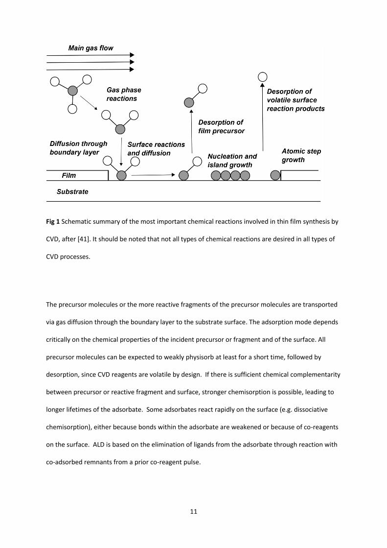
4. Chemical processes in CVD
Thin film growth by CVD is the result of a complex sequence of chemical reactions. All CVD processes
involve surface chemical processes and most CVD processes, with the exception of pure ALD
processes, involve also gas phase chemical reactions. The types of chemical reactions that have been
recognized as playing a role in CVD are schematically summarized in Fig. 1. Such a conceptual
scheme is generally the starting point for building theoretical models of the process. It is therefore
important to test the relative importance of these chemical processes in the deposition of a given
material system.
An important feature of CVD is that a boundary layer develops above the substrate surface, also
known as stagnant boundary layer. The development of this layer is a consequence of the fluid
dynamics when flowing a gas mixture above the surface [11]. In the boundary layer the velocity of
species in the flow direction is significantly lower than that in the main gas stream and the
concentration of species differs substantially compared to the main body of the gas stream. It is
generally considered that all chemistry of importance to the CVD process takes place in the boundary
layer and on the substrate surface.
In most, but not all, CVD processes the precursors undergo gas phase chemical reactions that result
in the formation of more reactive species. The reactions may be activated thermally or by an external
10
source of energy, e.g. application of a plasma. Generally these more reactive species are smaller
fragments of the original molecule and when a plasma is used to activate the chemistry the
molecular fragments can even be radicals or ions. One should bear in mind here that many CVD
processes are done at low pressures and high temperatures, allowing a significant lifetime of very
reactive species, compared to many other chemical reaction environments in e.g. a liquid solution. It
should be mentioned that for some CVD chemistries, the gas phase chemistry produces larger
complexes of several precursor molecules that after some molecular re-arrangements are the species
active in film deposition [39]. When hydrogen is used as carrier gas it often takes part in the gas
phase reactions, but even relatively inert nitrogen gas can in some thermally activated CVD processes
function as both carrier gas and film precursor. A mixture of hydrogen and nitrogen is then used as
carrier gas and only a very small fraction of the nitrogen molecules react to form the film.
The use of a plasma to activate the gas phase chemistry, as in PECVD, opens up several new reaction
paths at significantly lower temperatures, mainly by electron impact collisions but also by collisions
between plasma ions and precursor molecules, and by ions or radicals reaching the surface [5]. The
effect of the plasma is therefore often controlled by the distance between plasma and substrate in
the reactor; if the substrate is placed in the plasma or very close to the plasma (“direct PECVD”), ionic
species will significantly contribute to the chemistry, both in the gas phase and on the surface. A
longer distance between plasma and substrate (“remote PECVD”) leads to more significant
contribution from radical species rather than ions. It should be noted also that the power supplied to
the plasma discharge will change the amount of ions in the plasma and thereby also the ionic
contribution to the film growth chemistry [40]. In PECVD, dinitrogen gas is often used as nitrogen
precursor since the molecule rather easily dissociates in the plasma.
11
Fig 1 Schematic summary of the most important chemical reactions involved in thin film synthesis by
CVD, after [41]. It should be noted that not all types of chemical reactions are desired in all types of
CVD processes.
The precursor molecules or the more reactive fragments of the precursor molecules are transported
via gas diffusion through the boundary layer to the substrate surface. The adsorption mode depends
critically on the chemical properties of the incident precursor or fragment and of the surface. All
precursor molecules can be expected to weakly physisorb at least for a short time, followed by
desorption, since CVD reagents are volatile by design. If there is sufficient chemical complementarity
between precursor or reactive fragment and surface, stronger chemisorption is possible, leading to
longer lifetimes of the adsorbate. Some adsorbates react rapidly on the surface (e.g. dissociative
chemisorption), either because bonds within the adsorbate are weakened or because of co-reagents
on the surface. ALD is based on the elimination of ligands from the adsorbate through reaction with
co-adsorbed remnants from a prior co-reagent pulse.
12
Adsorbate molecules or fragments may be mobile on the surface and may sample a variety of surface
sites via diffusion, which again may lead to reactions. In general, surface diffusion is the process that
leads ultimately to formation of a film of the target material. Finding the optimum adsorption site
via diffusion is particularly important in the growth of epitaxial thin films for electronics since the
crystalline quality of the film determines the performance of the final device. Finding optimum sites
is facilitated by a strong energetic driving force towards forming the target material from the
reagents. In ALD this has been described as ‘densification’, whereby the coordination number of the
constituent atoms increases from the low value of molecular precursors to the high value of the solid
product [42, 43].
An important aspect of thin film deposition is the growth mode of the film on a given substrate.
Fragments may aggregate into nuclei or islands, or may attach to an atomic step, or may favor a
uniform coating. Roughness will increase if subsequent growth is favored at islands. By contrast,
well-behaved ALD processes give conformal films that exactly follow the roughness of the substrate.
Ultimately the growth processes combine and dictate the larger-scale morphology of the as-grown
film (epitaxial crystal, polycrystalline or amorphous) but the factors determining this are not in
general well understood [4].
The parts of the precursor molecule (e.g. the ligands) that do not constitute the target material
should then desorb from the film surface as by-products. These by-products can be simple molecules
formed by the chemical reactions on the surface, e.g. H2, CO2 or Cl2, or can be large molecules
derived from the ligands. For example, a protonated ligand is the by-product in thermal ALD of metal
oxides using H2O as co-reagent. In any case it is of great importance to all CVD processes that these
by-products desorb cleanly from the film surface and are not incorporated as impurities in the film.
13
5. The use of theoretical studies development and understanding of CVD processes
The main motivation for theoretical chemical studies of CVD processes is obtaining a detailed
understanding of the chemical reactions summarized in Fig. 1. There are various outcomes from
obtaining this understanding, as shown in the following examples.
A better understanding of established CVD processes
Thermochemical modeling of the gas phase chemistry in CVD is a convenient approach for
understanding the gas chemistry, given that not many experimental techniques are available.
Spectroscopic technique e.g. Raman or FT-IR spectroscopy could in principle be used but this requires
that all molecules in the gas phase can be detected by these techniques and that the CVD reactor can
be fitted with viewports of a material that is both transparent for the excitation light and at the same
time not affected by the CVD gases and process temperatures. A mass spectrometer measuring the
gas flow could also be used to study the process chemistry; the problem with this is that only the
stable molecules are detected while all unstable intermediates are lost. An example of a CVD process
where much understanding has been provided by thermochemical modeling is CVD of electronic
grade SiC. Significant effort has been directed towards understanding the process and a gas-phase
and surface reaction model has been proposed [44]. By using this model, the CVD process can be
discussed based on the gas phase and surface chemistry, rather than susceptor design and gas flow
patterns. Modeling can then be used to predict growth rate, etching rate, surface morphology and
doping, all key aspects when doing CVD of electronic device structures. Detailed gas phase chemistry
models can also be obtained by quantum chemical calculations, an example is the gas chemistry
model for CVD of boron carbide from BCl3 and C3H8 involving 16 intermediates presented in ref 45.
Consider the CVD of Al2O3 from AlCl3 and CO2, which has mainly been developed by research
departments in the hard coatings industry. CO2 forms H2O and CO together with the hydrogen carrier
14
gas in a gas phase reaction in the reactor and H2O then acts as the oxygen precursor in the formation
of Al2O3. The catalytic effect of H2S in this process has been known for many years. The addition of
H2S leads to a higher deposition rate and more surface controlled deposition process as evidenced by
more uniform coating thickness on complex substrate geometries [46]. But since this process was
mainly developed in industry, where detailed understanding often has low priority, it was only lately
that a surface chemical model supported by careful theoretical chemistry modeling could be
presented [47]. It was suggested that H2S acts as a true surface catalyst by facilitating first the
removal of adsorbed chlorine from the surface and then the adsorption of H2O. Another example
where modeling has been able to explain details in CVD of hard coatings is the observation that thin
films of titanium carbide grow along the (111) direction when aromatic hydrocarbons such as
benzene are used, while aliphatic hydrocarbons, e.g. methane, produce growth in the (100) direction.
This is of interest since (111) TiC performs better in cutting operations [48] and since control of the
preferred TiC growth direction enables control of the preferred growth direction of alumina
deposited on top of the TiC layer [49]. The explanation for the change in preferred growth direction
with aromatic hydrocarbons, provided by quantum chemical calculations, was that benzene
chemisorbs significantly more strongly on the (111) surface compared to the (100) surface and
reduces the surface energy of the (111) surface. [50] Methane did not show any significant
preference for either surface, so the lower surface energy of the (100) surface controls the growth
direction when aliphatic hydrocarbons are used. Although these findings on the surface chemistry
are not likely to change the well-established and optimized CVD process for industrially-used hard
coatings, such deeper understanding of the chemistry can serve as a guide for design of future CVD
processes.
15
Using modelling for designing new CVD processes
Theoretical studies of CVD surface chemistry that is more directed towards designing a new CVD
process for a material are the theoretical studies of CVD of cubic boron nitride (c-BN) onto diamond
surfaces. Models are developed of both the initial growth stage onto a diamond surface [51], and of
the subsequent growth of c-BN onto c-BN [52, 53], including surface reconstructions induced by
adsorption of precursor molecules onto c-BN [54,55]. The authors of these studies boil down their
results to a suggested ALD chemistry for deposition of c-BN [52], although it remains to be seen if it
will be tested given the large amount of HF produced as by-product.
When developing precursors for new CVD processes, modeling can give a better understanding of
the behavior of the molecules. It is especially important to understand how the molecules behave
upon vaporization and in the vapor phase. One such example is the development of CVD precursors
for metal boride films of the actinides and lanthanides [56, 57], where DFT modeling provided a
better understanding of why the same type of organometallic molecule works as CVD precursor for
Sm, Pr and Er but decomposes instead of subliming for U. [58]
Approaches exist for the simulation of gas-liquid equilibria for small molecules [59], which allow the
vapor pressure to be predicted. Extending these to metalorganic molecules requires accurate
estimation of both metal-ligand bonding and intermolecular interaction, and therefore requires an
approach beyond standard density functional theory. Simulating hundreds of molecules at such a
high level is currently beyond routine computational capacity.
ALD development and understanding
Given its great importance for the electronics industry, ALD is today the field of CVD where perhaps
the largest amount of effort is being directed towards increased understanding of the process
chemistry. Research on ALD is somewhat simplified by the surface controlled nature of the process –
16
at least in the ideal case – so that growth should be independent of other factors such as gas phase
chemistry and gas flow in the reactor. However the stringent and partially contradictory
requirements for achieving ALD make it very difficult to design a new process, even when theory and
experiment work closely together.
Since the earliest days of ALD research, atomic-scale models have been made of the underlying
chemistry. Pioneering calculations were carried out on the zinc sulfide system by T. Pakkanen and M.
Lindblad in the 1980’s [60,61]. Over 150 publications modelling ALD have followed since then, mostly
carrying out quantum chemistry on the reactions of precursors with model substrates and many of
these concerned with high-permittivity dielectrics on silicon. The state of the art to 2012 is
summarized in ref 62. Since then, our most recent atomic-scale simulations have revealed new
details of the mechanism of oxide ALD [43], have accounted for the stoichiometry of ternary oxides
[63], have assessed precursor ligands for alkaline earth metal oxides [64] and for copper metal [65]
and have developed kinetic Monte Carlo models of film growth [66].
The ALD process is manifest across many length scales. The pulsed flow of gases into meter-scale
reactors, around millimetre-scaled geometries, leads to chemical reactions between atoms, which
grow into nanometre-thick films and coat micron-scaled pores or particles. It is clearly impossible to
describe explicitly all of these length scales in one model, and most simulations are ‘multi-scale’
insofar as they involve coupling between selected length scales according to the property of interest.
The problem of timescale in ALD is perhaps even more acute than that of length scale, since a
combination of fast (ps-ns) and slow reactions (s-ms) contribute to film growth, and gases are
pulsed and purged over second-long timescales. Well-behaved ALD processes are independent of
reactor conditions, and so modelling ALD chemistry exclusively at the atomic scale can in fact explain
many features of film growth, without reference to reactor conditions. Nevertheless, explaining
ALD’s unique selling point – conformal and uniform growth regardless of the size and shape of the
17
substrate – requires modelling at higher length scales, ideally incorporating information about the
reaction chemistry from the atomic scale.
6. An overview of the special collection of papers on CVD and ALD modelling
This overview strives to aid readers with little or no experience in CVD and ALD and to put this special
collection of papers on CVD and ALD modelling into a broader perspective. The special collection has
been edited by the authors of this overview who also invited well known researchers in the field of
CVD/ALD modelling to submit original research manuscripts for the special collection. The collection
consists of nine papers on both CVD and ALD modelling, summarized below.
Two papers strive to shine light on the CVD process for epitaxial film growth of silicon carbide (SiC)
for manufacturing of high power electronic devices. The first paper by Danielsson et al. points to
several weaknesses of the thermo chemical modelling of SiC CVD heavily used in process
development today [67]. One of the main weaknesses is the suggested underestimation of the
surface reactivity of hydrocarbons in today’s modelling. Also, the great influence the quality of the
molecular data used has on the continuous flow dynamics (CFD) simulations is pointed out by using
state of the art quantum chemical calculations to provide more accurate molecular data. The other
paper on SiC CVD is a quantum chemical approach by Kalered et al. to better understand the effect of
using a chlorinated growth chemistry in SiC CVD [68]. The use of chlorinated growth chemistry also
for electronic grade SiC has enabled growth rates of 100 µm/h or higher [69], but the effect on the
surface chemistry when adding the chlorine has not been investigated before. It is shown in the
paper that SiCl2, the main Si species for a chlorinated chemistry, once chemisorbed has a higher
energy barrier for desorption compared to SiH2, the main Si species for the standard chemistry. It is
therefore suggested that the chlorinated chemistry can bring a more favorable surface chemistry to
SiC CVD.
18
An industrial CVD process where chlorinated chemistry is well established is CVD of α-Al2O3 for hard
coatings, C. Århammar et al. used a combination of thermochemistry and first principles modelling to
study possible point defects incorporated in the α-alumina films from the CVD gas mixture [70].
Besides Al and O, the gas mixture for alumina CVD contains H, C, Cl and S, but little is known on the
solubility of the possible point defects that can be created from these atoms. It is found that
especially interstitial hydrogen and chlorine have the lowest formation energies and are thus likely to
form, whereas sulfur from H2S, which act as catalyst in the process [47], is not likely to incorporate in
α-alumina.
R. Boichot et al. used thermochemical modelling to better understand a newly developed high
temperature CVD process for aluminum nitride (AlN) [71]. Of especial interest to model where
conditions in the boundary layer and close to the surface – parameters very hard to extract from
experiments. The modelling results were used to design validation experiments presented in the
paper. Even though the authors can deduce some experimental parameters needed for deposition of
high quality AlN and further reactor development, they also state that the modelling used fail to give
the whole picture since surface diffusion mechanisms are not included.
CVD is the standard technique for synthesizing thin films of diamond, a topic studied by Z. Yiming et
al. using DFT [72]. Particularly, the authors study the experimentally reported significant increase in
growth rate of diamond when adding nitrogen to the CVD gas mixture, however, from experiments it
is not clear if it is nitrogen incorporated into the diamond lattice or nitrogen, in the form of N, NH or
NH2, chemisorbed to the diamond surface that leads to the higher growth rate. The authors
conclude from their studies that nitrogen incorporated into the diamond lattice one or two atomic
layers beneath the surface gives a higher surface reactivity leading to a higher growth rate. The
authors estimate that the growth rate on the (100) surface of diamond will increase with a factor of
3.7 which is well in agreement with experimental findings.
19
J.-M. Lin and A. V. Teplyakov used density functional theory to explore the reactions of two
representative precursors with silicon surfaces terminated with various functionalities (Si-H, Si-N, Si-
O), yielding an impressive comparison across 32 reaction pathways [73]. The use of small Si clusters
as substrate models is discussed. The results for the trimethylaluminum precursor illustrate how
relatively simple C–Al and C–H dissociation processes are affected by the silicon termination.
Extending this to tetrakis(dimethylamido)titanium introduces more complex chemistry and provides
an opportunity to decouple electronic and steric factors. Molecular adsorption is seen to depend
strongly on the electron-donating properties of the substrate, consistent with frontier orbital
analysis. For proton transfer from substrate to ligand (the dominant ALD reaction), all activation
energies relative to molecular adsorption are computed to be greater than 50 kJ/mol, with the
exception of three pathways involving the Ti precursor and an O-terminated silicon surface.
The reaction kinetics of atomic layer deposition are described analytically and numerically in this
issue by C. D. Travis and R. A. Adomaitis [74]. Taking alumina deposition from trimethylaluminum
(TMA) as the sample system, a model describing the reaction kinetics and surface species dynamics
for the TMA half-reaction is developed. Four TMA reactions are included, accounting for TMA
adsorption and subsequent reaction on a range of growth surfaces spanning bare to fully
hydroxylated states. Published reaction energetics for these reactions from quantum chemical
studies are converted into kinetic parameters using statistical thermodynamics and absolute reaction
rate theory. The cyclic nature of ALD can be exploited to determine the overall growth rate from the
concentrations of surface species. Interestingly, the model reveals that substantial growth of alumina
is possible regardless of the level of hydroxylation of the substrate, as there are two competing
pathways with favourable kinetics. The reaction rate expressions developed here can be
implemented into reactor-scale simulations, which can guide the optimization of commercial ALD
processes.
20
An approach towards precursor design from first principles is outlined by G. Dey and S. D. Elliott in
this issue [75]. The subject is the ALD of metallic copper, where of course the precursor combination
must provide both copper cations and electrons for reduction to the metal. Here it is proposed that
the electron source should also contain copper, thus removing the chance of contamination by other
metals, but that this is pulsed alternately with a ‘standard’ copper source in 2-step or 3-step ALD. The
hydride anion is proposed as the reducing agent, as this may provide both electrons for reduction
and protons for elimination of ligands from the standard copper precursor. A copper carbene
complex is computed to yield maximal activation of the hydride and lead to volatile by-products, and
so the proposed precursor is 1,3-diphenyl-4,5-imidazolidinedithione copper hydride.
The paper in this issue by Yangas-Gil and Elam [76]highlights that simple first-order Langmuir kinetics
is sometimes insufficient to capture the complexities of ALD surface chemistry, especially when
precursor exposure is high, but that understanding such non-ideal cases is crucial for optimization
and reliability of commercial ALD processes. The authors’ approach is to cast gas transport inside
nanostructures as a single particle discrete Markov chain process, decoupled from reaction
mechanisms that can include branching and non-ideal surface kinetics as needed. This description of
surface chemistry is applicable generally to all types of CVD, not just ALD. A link is established
between ballistic models, kinetic Monte Carlo simulations, and continuous models based on the use
of the diffusion equation under Knudsen conditions. The calculations confirm that ALD coverage
depends solely on total exposure as long as reaction probabilities are pressure-independent.
7. Concluding remarks
There is substantial variation in our level of understanding of CVD and ALD processes: some
processes are investigated in great detail and are well understood, while others have been tuned to
perfection over many years of development and/or commercialization, without much understanding
of the details. In this overview, we have tried to point out the effectiveness and versatility of
21
theoretical chemistry as a tool to obtain a deeper understanding without experiments that require
highly complex equipment and conditions far from what is used in the actual deposition process. The
importance of CVD and ALD processes for our everyday lives is enormous and the continuing
development of e.g. electronics require constantly better CVD and ALD processes.Theoretical
chemistry modeling will play a key part in this development.
Acknowledgements
S. D. Elliott would like to acknowledge financial support from Science Foundation Ireland under the
ALDesign project, 09/IN.1/I2628, http://www.tyndall.ie/aldesign .
References
[1] Ohring M (2006) Materials Science of Thin Films 2nd ed. Elsevier, Singapore
[2] Martin PM (2010) Handbook of Deposition Technologies for Films and Coatings 3rd ed. Elsevier,
Amsterdam
[3] George SM (2010) Atomic Layer Deposition: An overview. Chem. Rev. 110:111-131
[4] Miikkulainen V, Leskelä M, Ritala M, Puurunen RL (2013) Crystallinity of inorganic films grown by
atomic layer deposition: Overview and general trends. J. Appl. Phys. 113:021301
[5] Hess W, Graves DB (1993) In: Hitchman ML and Jensen KF (eds.) Chemical Vapor Deposition:
Principles and Applications. Academic Press, San Diego
[6] Irvine SJC, Lamb D (2009) In: Jones AC and Hitchman ML (eds.) Chemical Vapour Deposition:
Precursors, Processes and Applications. Royal Society of Chemistry, Cambridge
[7] Hitchman ML and Jensen KF (eds.) (1993) Chemical Vapor Deposition: Principles and Applications.
Academic Press, San Diego
22
[8] Jones AC and Hitchman ML (eds.) (2009) Chemical Vapour Deposition: Precursors, Processes and
Applications. Royal Society of Chemistry, Cambridge
[9] Xu Y, Yan XT (2010) Chemical Vapour Deposition: An Intergrated Engineering Design for Advanced
Materials. Springer, London
[10] Dobkin DM, Zuraw MK (2003) Principles of Chemical Vapor Deposition: What’s Going on Inside
the Reactor. Kluwer Academic Publishers, Dordrecht
[11] Carlsson JO, Martin PM (2010) In: Martin PM (ed.) Handbook of Deposition Technologies for
Films and Coatings 3rd ed. Elsevier, Amsterdam
[12] Choy KL (2003) Chemical vapour deposition of coatings. Prog. Mater. Sci. 48:57-170
[13] Gates SM (1996) Surface chemistry in the chemical vapor deposition of electronic materials.
Chem. Rev. 96:1519-1532
[14] Carlsson JO, Jansson U (1993) Progress in chemical vapor deposition. Prog. Solid St. Chem.
22:237-292
[15] Stringfellow GB (2001) Fundamental aspects of organometallic vapor phase epitaxy. Mater. Sci.
Eng. B 87:97-116
[16] Kafizas A, Carmalt C J, Parkin I P (2013) CVD and precursor chemistry of transition metal nitrides.
Coord. Chem. Rev. 257:2073-2119
[17] Coordination Chemistry Reviews vol 257, issue 23-24, pp 3153-3384 (2013) contains 11 invited
reviews on CVD and ALD under the title ”Chemical Vapor Deposition and Atomic Layer Deposition:
Precursor Design and Application”
[18] Leskelä M, Ritala M (2002) Atomic layer deposition (ALD): from precursors to thin film
structures. Thin Solid Films 409:138-146
[19] Leskelä M, Ritala M (2003) Atomic Layer Deposition Chemistry: Recent Developments and Future
Challanges. Angew. Chem. Int. Ed. 42:5548-5554
[20] Puurunen RL (2005) Surface chemistry of atomic layer deposition: A case study for the
trimethylaluminum/water process. J. Appl. Phys. 97:121301

23
[21] Profijt HB, Potts SE, van de Sanden MCM, Kessels WMM (2011) Plasma-Assisted Atomic Layer
Deposition: Basics, Opportunities and Challanges. J. Vac. Sci. Tech. A 29:050801
[22] Zaera F (2012) The Surface Chemistry of Atomic Layer Depositions of Solid Thin Films. J. Phys.
Chem. Lett. 3:1301-1309
[23] Blocher JM (1997) Recollections of CVD conferences. Chem. Vap. Deposition 3:161-166
[24] Blocher JM (1974) Structure/property/process relationships in chemical vapor deposition CVD. J.
Vac. Sci. Tech. 11:680-686
[25] Jones AC, Hitchman ML (2009) In: Jones AC and Hitchman ML (eds.) (2009) Chemical Vapour
Deposition: Precursors, Processes and Applications. Royal Society of Chemistry, Cambridge
[26] Allendorf M (1998) From Bunsen to VLSI. The Electrochemical Society Interface 7:36-39
[27] Wöhler F, Uslar L (1855) Über metallisches Wolfram und Molybdän. Just. Lieb. Ann. Chem.
94:255-259
[28] Mond L, Langer C, Quincke F (1890) Action of Carbon Monoxide on Nickel. J. Chem. Soc. 57:749-
753
[29] Mond L (1891) Process of depositing nickel. U.S. Patent 455,230
[30] Pring JN, Fielding W (1909) The Preparation at High Temperatures of some Refractory Metals
from their Chlorides. J. Chem. Soc.95:1497-1506
[31] Manasevit HM (1968) Singel-Crystal Gallium Arsenide on Insulating Substrates. Appl. Phys. Lett.
12:156-159
[32] Suntola T, Antson J (1977) Method for producing compound thin films. U.S. Patent 4,058,430
[33] Ritala M, Niinistö J (2009) In: Jones AC and Hitchman ML (eds.) Chemical Vapour Deposition:
Precursors, Processes and Applications. Royal Society of Chemistry, Cambridge
[34] Bohr MT, Chau RS, Ghani T, Mistry K (2007) The high-k solution. IEEE Spectrum 44:29-35
[35] Ruppi S (2008) Enhanced performance of α-Al2O3 coatings by control of crystal orientation. Surf.
Coat. Technol. 202:4257-4269
24
[36] Parkin IP, Palgrave RG (2009) In: Jones AC and Hitchman ML (eds.) Chemical Vapour Deposition:
Precursors, Processes and Applications. Royal Society of Chemistry, Cambridge
[37] Groner MD, Fabreguette FH, Elam JW and George SM (2004) Low-Temperature Al2O3 Atomic
Layer Deposition. Chem. Mater. 16:639–645.
[38] Park JS, Chae H, Chung HK and Lee SI (2011) Thin film encapsulation for flexible AM-OLED: a
review. Semicond. Sci. Technol. 26:034001.
[39] Kakanakova-Georgieva A, Gueorguiev G, Stafström S, Hultman L, Janzén E (2006) AlGaInN metal-
organic-chemical-vapor-deposition gas-phase chemistry in hydrogen and nitrogen dilutents: First-
principles calculations. Chem. Phys. Lett. 431:346-351
[40] Pedersen H, Larsson P, Aijaz A, Jensen J, Lundin D (2012) A novel high-power pulse PECVD
method. Surf. Coat. Technol. 206:4562-4566
[41] Jensen KF (1993) In: Hitchman ML and Jensen KF (eds.) Chemical Vapor Deposition: Principles
and Applications. Academic Press, San Diego
[42] livier S, Duc r -M, Mastail C, Landa G, Est ve A, D afari Rouhani M (2008), Insights into
Crystalline Preorganization of Gas-Phase Precursors: Densification Mechanisms. Chem. Mater.
20:1555-1560
[43] Shirazi M, Elliott S D (2013) Multiple Proton Diffusion and Film Densification in Atomic Layer
Deposition Modeled by Density Functional Theory. Chem. Mater. 25:878–889
[44] Nishizawa S, Pons M (2006) Growth and doping modeling of SiC-CVD in a horizontal hot-wall
reactor. Chem. Vapor Deposition 12:561-522
[45] Jing X, Su K, Wang X, Wang Y, Liu Y, Zeng Q, Cheng L, Zhang L (2010) An investigation of the
lowest reaction pathway of propene + BCl3 decomposition in chemical vapor deposition process.
Theo. Chem. Acc. 127:519-538
[46] Mårtensson P (2006) Influence of the concentration of ZrCl4 on texture, morphology and growth
rate of CVD grown α-Al2O3 coatings deposited by the AlCl3/ZrCl4/H2/CO2/H2S process. Surf. Coat.
Technol. 200:3626-3632

25
[47] Blomqvist A, Århammar C, Pedersen H, Silvearv F, Norgren S, Ahuja R (2011) Understanding the
catalytical effects of H2S on CVD-growth of α-alumina: Thermodynamic gas-phase simulations and
density functional theory. Surf. Coat. Technol. 206:1771-1779
[48] Leonhardt A, Wolf E (1996) Influence of different hydrocarbons on the structure of CVD- and
PACVD-TiCx hard layers. Mater. Sci. Eng. A 209:389-393
[49] Canovic S, Ljungberg B, Halvarsson M (2011) CVD TiC/alumina mulitlayers grown on sapphire
single crystals. Micron 42:808-818
[50] Pedersen H, Lin CC, Ojamäe L (2013) On the change of preferential growth orientation in
chemical vapor deposition of titanium carbide by aromatic hydrocarbon precursors. J. Vac. Sci. Tech.
A 31:021507
[51] Pallas A, Larsson K (2010) Initial Growth of BN on Diamond Substrates: A Theoretical Approach.
J. Phys. Chem. C 114:11448-11455
[52] Karlsson J, Larsson K (2011) Adsorption of Growth Species on the c-BN (100) Surface. J. Phys.
Chem. C 115:16977-16983
[53] Karlsson J, Larsson K (2013) Kinetic considerations of gas-phase abstraction of H and F from the
c-BN (100) surface. Thin Solid Films 548:280-287
[54] Karlsson J, Larsson K (2010) Hydrogen-Induced De/Reconstruction of the c-BN (100) Surface. J.
Phys. Chem. C 114:3516-3521
[55] Karlsson J, Larsson K (2011) Halogen-Induced Reconstructionof the c-BN (100) Surface. J. Phys.
Chem. C 115:22910-22916
[56] Daly SR, Kim DY, Yang Y, Abelson JR, Girolami GS (2010) Lanthanide N,N-
dimethylaminodiboranates: highly volatile precursors for the deposition of lanthanide-containing
thin films. J. Amer. Chem. Soc. 132:2106-2107
[57] Daly SR, Kim DY, Girolami GS (2012) Lanthanide N,N-dimethylaminodiboranates as a new class of
highly volatile chemical vapor deposition precursors. Inorg. Chem. 51:7050-7065
26
[58] Vlaisavljevich B, Miró P, Koballa D, Todorova T, Daly SR, Girolami GS, Cramer CJ, Gagliardi L
(2012) Volatilities of Actinide and Lanthanide N , N -Dimethylaminodiboranate Chemical Vapor
Deposition Precursors: A DFT Study. J. Phys. Chem. C 116:23194-23200
[59] McGrath M J, Kuo I-F W, Ghogomu J N, Mundy C J, Siepmann J I (2011) Vapor-liquid coexistence
curves for methanol and methane using dispersion corrected density functional theory. J. Phys.
Chem. B 115:11688-11692
[60] Pakkanen T, Lindblad M, Nevalainen V (1984) Quantum chemical studies of the formation of zinc
sulfide surface by the ALE technique. First Symposium on Atomic Layer Epitaxy, VTT Symposium 54,
Espoo, Finland, 13-14 December
[61] Lindblad M, Pakkanen T A (1988) Surface model for ZnS thin films: ZnS clusters and
chemisorption of ZnCl2 on ZnS surface. J. Comp. Chem. 9:581-590
[62] Elliott S D (2012) Atomic-scale simulation of ALD chemistry. Semicond. Sci. Technol. 27:074008
[63] Murray C, Elliott S D (2013) Density Functional Theory Predictions of the Composition of ALD-
grown Ternary Oxides. ACS Appl. Mater. Interfaces 5:3704–3715
[64] Kazadojev I, Otway D J, Elliott S D (2013) Modeling of Precursors for Atomic Layer Deposition of
Magnesium and Calcium Oxide. Chem. Vap. Depos. 19:117–124
[65] Dey G, Elliott S D (2012) Mechanism for the atomic layer deposition of copper using diethylzinc
as the reducing agent: a density functional theory study using gas-phase molecules as a model. J.
Phys. Chem. A 116:8893–8901
[66] Shirazi M, Elliott S D (2014) Atomistic kinetic Monte Carlo study of atomic layer deposition
derived from density functional theory. J. Comp. Chem. 35:244259
[67] Danielsson Ö, Sukkaew P, Ojamäe L, Kordina O, Janzén E (2013) Shortcomings of CVD modelling
of SiC today. Theo. Chem. Acc. 132:1398
[68] Kalered E, Pedersen H, Janzén E, Ojamäe L (2013) Adsorption and surface diffusion of silicon
growth species in silicon carbide chemical vapour deposition processes studied by quantum-chemical
computations. Theo. Chem. Acc. 132:1403

27
[69] Pedersen H, Leone S, Kordina O, Henry A, Nishizawa S, Koshka Y, Janzén E (2012) Chloride-based
growth of silicon carbide for electronic applications. Chem. Rev. 112:2434-2453
[70] Århammar C, Silvearv F, Bergman A, Norgren S, Pedersen H, Ahjua R (2014) A theoretical study
of possible point defects incorporated into α-alumina deposited by chemical vapor deposition. Theo.
Chem. Acc. 133:1433
[71] Boichot R, Coudurier N, Mercier F, Claudel A, Baccar N, Milet A, Blanquet E, Pons M (2014) CFD
modeling of the high-temperature HVPE growth of aluminum nitride layers on c-plane sapphire: from
theoretical chemistry to process evaluation. Theo. Chem. Acc. 133:1419
[72] Yiming Z, Karlsson F, Larsson K (2014) Effect of CVD diamond growth by doping with nitrogen.
Theo. Chem. Acc. 133:1432
[73] Lin J-M, Teplyakov A V (2013) Computational investigation of surface reactivity of functionalized
silicon surfaces in deposition processes. Theo. Chem. Acc. 132:1404
[74] Travis C D, Adomaitis R A (2014) Modeling alumina atomic layer deposition reaction kinetics
during the trimethylaluminum exposure. Theo. Chem. Acc. 133:1414
[75] Dey G, Elliott S D (2014) Copper(I) carbene hydride complexes acting both as reducing agent and
precursor for Cu ALD: a study through density functional theory. Theo. Chem. Acc. 133:1416
[76]Yanguas-Gil A, Elam J W (2014) A Markov chain approach to simulate Atomic Layer Deposition
chemistry and transport inside nanostructured substrates. Theo. Chem. Acc. 133:1465