study of the interface microstructures of cvd diamond films by tem
TRANSCRIPT

Study of the Interface Microstructures of CVD Diamond Films by TEM
Alexander G. Fitzgerald1;�, Yongchang Fan1, Phillip John2, Clare E. Troupe2, John I. B. Wilson3,
Anthony O. Tooke1, and Brian E. Storey1
1 Department of Applied Physics and Electronic & Mechanical Engineering, University of Dundee, Dundee DD1 4HN, UK2 Department of Chemistry, Heriot-Watt University, Edinburgh EH14 4AS, UK3 Department of Physics, Heriot-Watt University, Edinburgh EH14 4AS, UK
Abstract. The characteristics of the interface micro-
structures between a CVD diamond ®lm and the silicon
substrate have been studied by transmission electron
microscopy and electron energy loss spectroscopy. The
investigations are performed on plan-view TEM speci-
mens which were intentionally thinned only from the
®lm surface side allowing the overall microstructural
features of the interface to be studied. A prominent
interfacial layer with amorphous-like features has been
directly observed for CVD diamond ®lms that shows a
highly twinned defective diamond surface morphol-
ogy. Similar interfacial layers have also been observed
on ®lms with a h100i growth texture but having the
{100} crystal faces randomly oriented on the silicon
substrate. These interfacial layers have been unam-
biguously identi®ed as diamond phase carbon by both
electron diffraction and electron energy loss spectros-
copy. For the CVD diamond ®lms that exhibit hetero-
epitaxial growth features, with the {100} crystal faces
aligned crystallographically on the silicon substrate,
such an interfacial layer was not observed. This is
consistent with the expectation that the epitaxial
growth of CVD diamond ®lms requires diamond crys-
tals to directly nucleate and grow on the substrate
surface or on an epitaxial interface layer that has a
small lattice mis®t to both the substrate and the thin
®lm material.
Key words: CVD diamond ®lms; interface microstructure; trans-mission electron microscopy; electron energy loss spectroscopy.
A particularly useful application of the transmission
electron microscope (TEM) in CVD diamond ®lm
studies is in the investigation of the characteristics of
the interface between the diamond ®lm and the
associated substrate. Information on interface micro-
structural properties of the ®lms is usually obtained by
cross-sectional TEM (XTEM) observations. In a few
cases, epitaxial growth of CVD diamond ®lms directly
onto certain kinds of substrates such as single crystal
Pt (111) and cubic boron nitride has been con®rmed
by TEM observations [1 ± 2]. However, in the majority
of XTEM investigations, the diamond crystal grains
were not found to be in direct contact with the
substrate. There is an interfacial layer between the
substrate and the diamond crystal, and the structure of
the interfacial layer is strongly in¯uenced by the
deposition conditions.
In some situations, the interfacial layer that exists
between the diamond ®lm and the silicon substrate
has been identi®ed as epitaxial silicon carbide [3 ± 5].
However, in many cases, the microstructures observed
at the interface were found to be more complicated
and the interfacial layer on which the diamond
crystallite can nucleate and grow cannot be simply
classi®ed as silicon carbide [6]. Diamond ®lms have
also been observed to grow on amorphous silicon
carbide [5], amorphous carbon [4] and on `diamond-
like' carbon [7] interfacial layers.
The microstructural information on the interface
between a silicon substrate and a diamond ®lm has
been obtained exclusively by cross-sectional TEM
observations. This type of observation is not easily
performed in practice because of the dif®culties
Mikrochim. Acta 132, 315±321 (2000)
� To whom correspondence should be addressed

involved in the preparation of cross-sectional TEM
specimens. In many cases, the composition and phase
of the observed layer cannot be identi®ed by electron
diffraction or electron energy loss spectroscopy
because of the small cross-sectional dimensions of
the interface layers. Also, the overall microstructural
properties of the interface layer usually cannot be
obtained by cross-sectional TEM observations.
In this paper, we report on microstructural studies
of the interface by plan-view TEM observations. In
these studies, some plan-view TEM specimens were
intentionally thinned only from the ®lm surface side
allowing the overall microstructural features of the
interface to be directly observed. In these investiga-
tions, special attention has been focused on the
correlation of the ®lm growth textures with the
microstructural properties of the interface.
Experimental
The diamond ®lms investigated in this work were prepared on asilicon (100) substrate by a three stage process i.e. carburisation,biasing nucleation and growth in a UHV compatible depositionsystem which has been constructed for the growth of diamond by2.45 GHz microwave plasma enhanced chemical vapour deposition[8 ± 10]. The prepared CVD diamond ®lms can be visualised to beroughly composed of two distinct growth regions i.e. a centralgrowth region with a diameter of about 4 ± 6 mm that has a deepdark colour and an annular ring region with a band width of 4 to5 mm that has a shiny grey colour. AFM observations show that the®lms deposited in these two regions have a different growthtexture. Also, the surface morphology changes greatly with theposition along radial directions within each growth region.
By fracturing the diamond film and substrate, some pieces offree-standing diamond film could be obtained. For plan-view TEMobservations, specimens from these pieces of free-standingdiamond film were sandwiched in a folding copper electronmicroscope grid and then thinned by ion milling with a 5 keVargon ion beam, at 20� incidence until perforation. The free-standing diamond films for TEM specimen preparation wereintentionally chosen respectively from the central growth regionand the annular ring region to enable correlation of themicrostructural properties of the film with corresponding morpho-logical features. Some of the plan-view TEM specimens werethinned by ion etching only from the thin film surface side and thisenabled the microstructure in regions near to the diamond-siliconinterface to be studied. The TEM investigations were performed ona JEOL 200CX transmission electron microscope which wasoperated at 200 kV.
Results and Discussion
Diamond Films with a Highly Twinned
Defective Surface Morphology
Specimen I was taken from the central growth region
in a CVD diamond ®lm. Atomic force microscopy
(AFM) observations showed that the ®lm deposited in
this central region was mainly composed of randomly
oriented microcrystallites (Fig. 1a), and the ®lm
usually showed a highly twinned defective diamond
surface morphology. The corresponding microstruc-
tural features near to the interface for this ®lm are
shown in Fig. 1b and Fig. 1c. An intermediate layer
can be observed to exist in between the silicon
substrate and the ®ne diamond crystal grains. By
observation of the spherical-like appearance of the
deposits in this region, the interfacial layer appears
more likely to be amorphous than crystalline. From
the high magni®cation micrograph shown in Fig. 1c,
the larger round-shaped lumps with a size from a few
tens to several hundreds of nanometres appear to be
aggregated from much smaller clusters or blisters.
Electron diffraction analysis (see Fig. 1d) indicates
that the ®lm that initially grew at the interface region
was in fact polycrystalline diamond in nature. The
®rst four prominent diffraction rings in the electron
diffraction pattern have been indexed as due to
diffraction respectively from the cubic diamond
{111}, {220}, {311} and {222} lattice planes.
Diamond Films with a Predominant
h100i Growth Texture
Specimen II was taken close to the annular ring region
in a CVD diamond ®lm. The ®lm grown in this region
had a predominant h100i growth texture as illustrated
in Fig. 2a. The majority of the diamond crystal grains
formed in this region exhibited square or rectangular
(100) crystal faces which were approximately parallel
to the substrate surface. The existence of an inter-
mediate layer between the well-developed diamond
crystal grains and the silicon substrate can be seen
more clearly in this sample as shown in Fig. 2b to Fig.
2d. From these TEM micrographs, the observed dark
intermediate layer has an amorphous appearance.
However, subsequent electron diffraction and electron
energy loss spectroscopy (EELS) analysis indicated
that this intermediate layer was also mainly composed
of the polycrystalline diamond-phase carbon material.
From these TEM micrographs it can also be seen
that the specimen is not completely covered with this
intermediate layer. For this sample, whether or not the
interfacial layer can be observed in TEM images
seems to depend on whether or not this layer is
attached to the free-standing ®lm or is left on the
substrate during the diamond ®lm-substrate separation
316 A. G. Fitzgerald et al.

Fig. 1. Surface morphology andinterface microstructures for dia-mond ®lm specimen I, the diamond®lm thickness is about 12mm. (a)AFM topographic image of the ®lmsurface, (b and c) TEM micrographstaken from the interface, (d) elec-tron diffraction pattern taken fromthe area shown in (c)
Fig. 2. Surface morphology andinterface microstructures for dia-mond ®lm specimen II, the diamond®lm thickness is about 12mm. (a)AFM topographic image of the ®lmsurface, (b, c and d) TEM micro-graphs taken from the interfaceregion
Study of the Interface Microstructures of CVD Diamond Films by TEM 317

process. This speculation has been con®rmed by AFM
observations on the surface of the detached ®lm which
was in contact with the substrate and the substrate
surface from which the ®lm had been detached. When
the diamond ®lm was separated from the substrate, in
some areas, the interfacial layer is left on the
substrate, in other areas, the interfacial layer is
attached to the separated free-standing ®lm. For just
this reason, the interfacial layer without a diamond
®lm superimposed on it and the diamond layer
without the interfacial layer attached to it can be
observed and studied simultaneously on single TEM
plan-view specimen.
When an area that was not covered with this
intermediate layer was examined at high magni®ca-
tion, some large grain-like areas were observed as
illustrated in Fig. 3a. All of the large grain-like areas
consisted of several fan-shaped growth sections and
the fan-shaped growth sections in each grain-like area
emerged from a common centre within the grain.
Similar growth features near to the interface have also
been observed in other cross-sectional TEM investi-
gations [1, 2, 6]. Since the defects are generated
because of the growth species sitting at improper
lattice sites during the deposition process, the defect
lines in the fan-shaped growth section actually re¯ect
the trace of crystal growth. These observed features
imply that each diamond grain nucleates from a single
site and the diamond crystal grows in three-dimen-
sions [6]. The polycrystalline diamond nature of these
larger grain-like areas has been con®rmed from the
well-de®ned electron diffraction pattern obtained
from these grains shown in Fig. 3b.
For comparison, a high magni®cation TEM image
and corresponding electron diffraction pattern taken
from the intermediate layer are illustrated respectively
in Fig. 3c and Fig. 3d. The diffraction pattern taken
from the intermediate layer (Fig. 3d) is the same as
the pattern taken from diamond crystal grains
(Fig. 3b). So it can be inferred that the sp3 bonded
diamond phase is the main ingredient in the
intermediate layer.
The diamond nature of the intermediate layer has
been further con®rmed by electron energy loss
spectroscopy. The plasmon loss spectra taken from
the intermediate layer is exactly the same as that taken
Fig. 3. TEM micrographs and elec-tron diffraction patterns taken fromspecimen II, (a and b) from grain-like areas, (c and d) from the inter-facial layer
318 A. G. Fitzgerald et al.

from diamond crystal grains as shown in Fig. 4. The
characteristic loss peak at 34 eV, which is unique to
diamond and caused by bulk plasmon resonance of
valence electrons [11] can be observed to appear in
the spectra from both the diamond grain and the
interfacial layer. The peaks at around 65 eV and 99 eV
are also characteristic of diamond and are due to the
excitation of second and third plasmons. A similar
loss feature has also been observed on the carbon K-
edge electron energy loss spectra. The intermediate
layer that existed at the diamond-silicon interface can
therefore be unambiguously identi®ed as diamond
phase material.
Diamond Films with an Epitaxial
h100i Growth Features
Specimen III was also taken from the annular ring
region in a CVD diamond ®lm but the difference is
that this ®lm exhibited superior epitaxial growth as
shown in Fig. 5a and Fig. 5b. Most of the square-
shaped diamond crystal grains can be seen to be well
Fig. 4. Electron energy-loss spectra in the low energy loss regionof 0 to 150 eV, (a) taken from a large diamond crystal grain, (b)taken from the interfacial layer
Fig. 5. AFM images taken fromspecimen III, the diamond ®lmthickness is about 25 mm. (a and b)Images taken from the ®lm surface,(c and d) images taken from theinterface side of the ®lm, image scansize: (a) 30mm, (b) 10mm, (c) 40 mm,(d) 6.5 mm
Study of the Interface Microstructures of CVD Diamond Films by TEM 319

aligned with each other with their crystal edges
running in two predominant directions. These features
indicate that the diamond crystal grains, in this case,
grow epitaxially on the silicon substrate. The interface
side of the ®lm i.e. the surface that was in contact with
the silicon substrate before being detached was also
observed by AFM and the representative AFM images
are illustrated in Fig. 5c and Fig. 5d. From these AFM
images it can be seen very clearly that circle-like
marks appear at the centre on each of the large
diamond crystal grains. Each crystal grain is com-
posed of several fan-shaped growth sections that
radiate outward from the centres of the circles. It is
easy to speculate that these large diamond crystal
grains initially nucleate as a spherical cluster and then
grow in three dimensions outward until coalescence
occurs with the adjacent diamond crystal grains.
Two types of distinctive structural features were
observed at the interface in specimen III as shown in
Fig. 6. The TEM image in Fig. 6a was taken at low
magni®cation and shows the overall structural fea-
tures. In the central area of this image, some crystal
grains with fan-shaped contrast can be observed.
However, in peripheral areas the crystal grains have
been masked by some round-shaped clusters or
blisters. The details of the clusters or blisters are
illustrated in Fig. 6b which was taken from the
peripheral areas at an increased magni®cation. Even
though these features have an amorphous-like appear-
ance, electron diffraction analysis, however, showed
that these clusters were polycrystalline diamond. It
can be inferred therefore that these nanoscale blisters
or clusters are diamond phase.
Fig. 6c and Fig. 6d show typical TEM micrographs
taken from the majority of the areas in specimen III.
From these images, the diamond crystal grains and the
fan-shaped growth sections within the crystal grains
can be seen more clearly. These growth features
observed by TEM for diamond crystals close to the
interface are very similar to those that have been
observed by AFM. The difference is that in the AFM
observations, the image contrast was caused by the
surface roughness, while here in the TEM observa-
tions, the image contrast is produced by structural
defects.
From these TEM images it is proposed that
diamond phase material initially nucleates randomly
on the substrate surface forming tiny clusters. In the
Fig. 6 (a±d). TEM micrographstaken from specimen III showingthe interface microstructures of anepitaxial CVD diamond ®lm
320 A. G. Fitzgerald et al.
subsequent deposition process, these clusters develop
into large ball-like features by the continuous addition
of the deposited diamond component to these clusters.
With increase in the size of these ball-like features,
crystal facets gradually develop in certain favoured
directions. Because there is no con®nement of the
diamond crystal growth before coalescence, a high
density of defects will be accommodated within the
crystal grains. This is indeed true as all the electron
diffraction patterns taken from the crystal grain show
similar polycrystalline diamond diffraction patterns.
All of the diffraction rings can be identi®ed as
originating from diamond cubic lattice planes and no
other phases can be identi®ed.
Here, it should be emphasised that a prominent
intermediate layer has not been observed in this ®lm
although some cluster or blister-like features have
been observed on detached ®lms near to the interface.
There are some substantial morphological differences
between the diamond ®lm specimens III and II. The
crystal grains in specimen II are randomly oriented
while, the crystal grains in specimen III are well
aligned with each other showing typical epitaxial
growth features. From these considerations it seems
that a thick intermediate diamond phase carbon layer
does not exist in specimen III. It is highly improbable
that epitaxial diamond grains could grow on a
polycrystalline intermediate layer. Previous work
[12] has demonstrated the role of � silicon carbide
at the interface of diamond and silicon substrate.
Conclusions
In the TEM studies discussed here, some plan-view
TEM specimens have been prepared by ion thinning
only from the ®lm surface side to enable investigation
of the microstructural properties of the ®lm near to the
interface. The overall in-plan structural features of the
interfacial layer existing between the silicon and
diamond crystal grains was directly observed by this
plan-view TEM investigation. The polycrystaline
interfacial layer has been unambiguously identi®ed
as diamond phase carbon by both electron diffraction
and electron energy loss spectroscopy. These observa-
tions have con®rmed that the diamond crystal grains
in a diamond ®lm are not in direct contact with the
silicon substrate but instead form and grow on this
diamond phase carbon intermediate layer.
For the CVD diamond ®lm with epitaxial growth
features, no obvious interfacial intermediate layer was
observed. Epitaxial growth of the CVD diamond ®lm
required diamond crystals to nucleate directly and
grow on the substrate surface or on an epitaxial
interface layer which has a small lattice mis®t to both
the substrate and the thin ®lm material. Obviously, if
the interfacial layer is amorphous or polycrystalline in
nature, a crystallographic relation cannot be expected
between the diamond ®lm and the substrate. It can be
concluded that the elimination of the amorphous-like
interfacial layer at the earliest stage of deposition is
crucial to the heteroepitaxial growth of CVD diamond
®lms.
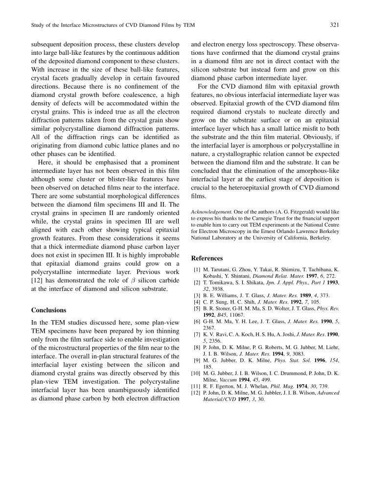
Acknowledgement. One of the authors (A. G. Fitzgerald) would liketo express his thanks to the Carnegie Trust for the ®nancial supportto enable him to carry out TEM experiments at the National Centrefor Electron Microscopy in the Ernest Orlando Lawrence BerkeleyNational Laboratory at the University of California, Berkeley.
References
[1] M. Tarutani, G. Zhou, Y. Takai, R. Shimizu, T. Tachibana, K.Kobashi, Y. Shintani, Diamond Relat. Mater. 1997, 6, 272.
[2] T. Tomikawa, S. I. Shikata, Jpn. J. Appl. Phys., Part 1 1993,32, 3938.
[3] B. E. Williams, J. T. Glass, J. Mater. Res. 1989, 4, 373.[4] C. P. Sung, H. C. Shih, J. Mater. Res. 1992, 7, 105.[5] B. R. Stoner, G-H. M. Ma, S. D. Wolter, J. T. Glass, Phys. Rev.
1992, B45, 11067.[6] G-H. M. Ma, Y. H. Lee, J. T. Glass, J. Mater. Res. 1990, 5,
2367.[7] K. V. Ravi, C. A. Koch, H. S. Hu, A. Joshi, J. Mater. Res. 1990,
5, 2356.[8] P. John, D. K. Milne, P. G. Roberts, M. G. Jubber, M. Liehr,
J. I. B. Wilson, J. Mater. Res. 1994, 9, 3083.[9] M. G. Jubber, D. K. Milne, Phys. Stat. Sol. 1996, 154,
185.[10] M. G. Jubber, J. I. B. Wilson, I. C. Drummond, P. John, D. K.
Milne, Vaccum 1994, 45, 499.[11] R. F. Egerton, M. J. Whelan, Phil. Mag. 1974, 30, 739.[12] P. John, D. K. Milne, M. G. Jubbler, J. I. B. Wilson, Advanced
Material/CVD 1997, 3, 30.
Study of the Interface Microstructures of CVD Diamond Films by TEM 321