study of bad block management and wear leveling in nand flash memories
TRANSCRIPT

IJRET: International Journal of Research in Engineering and Technology eISSN: 2319-1163 | pISSN: 2321-7308
__________________________________________________________________________________________
Volume: 02 Issue: 10 | Oct-2013, Available @ http://www.ijret.org 284
STUDY OF BAD BLOCK MANAGEMENT AND WEAR LEVELING IN
NAND FLASH MEMORIES
Supriya Kulkarni P1, Jisha P
2
1Student,
2Assistant Professor, Electronics & Communication Dept, MVJ College of Engineering, Bangalore, India
[email protected], [email protected]
Abstract NAND Flash devices have become preferred choice in high density, low cost and high read and write operations where in very large
sequential data has to repeatedly written and read at higher rate. However it is hindered by a character called “Lifetime”. Typically
NAND Flash devices wear out providing around 10,000 to 100,000 life cycles. In this paper we are concerned to discuss about the
techniques called Bad-Block Management (BBM) and Wear-leveling to increase the Lifetime of the NAND Flash memories.
Keywords: NAND Flash memory, BBM, Wear-leveling, Lifetime.
---------------------------------------------------------------------***------------------------------------------------------------------------
1. INTRODUCTION
FLASH memories are electronic nonvolatile storage devices
that can be electrically erased and reprogrammed. There are
two types of Flash memories: NOR Flash memory and NAND
Flash memory. Embedded systems have traditionally utilized
NOR devices. However, high density, low cost and high speed
READ/WRITE operations has moved the trend towards
NAND Flash device.
1.1 NOR Versus NAND Technology
There are specific advantages and disadvantages to in using
NAND Flash or NOR Flash in embedded systems. NAND
Flash is best suited for file or sequential-data applications;
NOR Flash is best suited for random access. The comparison
is tabulated in Table1. Even though NAND Flash devices has
disadvantages of Slow random access and Byte WRITEs
difficult, the real benefits of NAND Flash are faster
PROGRAM and ERASE times, as NAND Flash delivers
sustained WRITE performance exceeding 5 MB/s. Block erase
times are an impressive 2ms for NAND Flash compared with
750ms for NOR Flash. Clearly, NAND Flash offers several
compelling advantages
Table1. NOR versus NAND flash memories
As the quest continues for lower-power, lighter, more robust
products, NAND Flash will prove to be an ideal solution for a
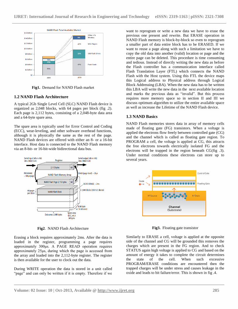
wider range of applications. Fig .1 shows how demand for
NAND Flash has been driven by three major markets-digital
camera media cards, USB flash drives, and MP3 players.
NAND Flash is better suited to meet the storage requirements
of many consumer audio and video products, especially low-
capacity applications (4GB or less).
NAND NOR
Advantages
Fast WRITEs Random access
Fast ERASEs Byte WRITEs
possible
Disadvantages
Slow random
access Slow WRITEs
Byte WRITEs
difficult Slow ERASEs
Applications
File (disk)
applications
Replacement of
EPROM
Voice, data,
video recorder
Execute directly
from nonvolatile
memory
IJRET: International Journal of Research in Engineering and Technology eISSN: 2319-1163 | pISSN: 2321-7308
__________________________________________________________________________________________
Volume: 02 Issue: 10 | Oct-2013, Available @ http://www.ijret.org 285
Fig1. Demand for NAND Flash market
1.2 NAND Flash Architecture
A typical 2Gb Single Level Cell (SLC) NAND Flash device is
organized as 2,048 blocks, with 64 pages per block (fig .2).
Each page is 2,112 bytes, consisting of a 2,048-byte data area
and a 64-byte spare area.
The spare area is typically used for Error Control and Coding
(ECC), wear-leveling, and other software overhead functions,
although it is physically the same as the rest of the page.
NAND Flash devices are offered with either an 8- or a 16-bit
interface. Host data is connected to the NAND Flash memory
via an 8-bit- or 16-bit-wide bidirectional data bus.
Fig2. NAND Flash Architecture
Erasing a block requires approximately 2ms. After the data is
loaded in the register, programming a page requires
approximately 300μs. A PAGE READ operation requires
approximately 25μs, during which the page is accessed from
the array and loaded into the 2,112-byte register. The register
is then available for the user to clock out the data.
During WRITE operation the data is stored in a unit called
“page” and can only be written if it is empty. Therefore if we
want to reprogram or write a new data we have to erase the
previous one present and rewrite. But ERASE operation in
NAND Flash memory is block-by-block so even to reprogram
a smaller part of data entire block has to be ERASED. If we
want to reuse a page along with such a limitation we have to
copy the old data into another (valid) location or page and the
entire page can be deleted. This procedure is time consuming
and tedious. Instead of directly writing the new data as before
the Flash controller has a communication interface called
Flash Translation Layer (FTL) which connects the NAND
Flash with the Host system. Using this FTL the device maps
this Logical address to Physical address through Logical
Block Addressing (LBA). When the new data has to be written
this LBA will write the new data in the next available location
and marks the previous data as “invalid”. But this process
requires more memory space so in section II and III we
discuss optimum algorithm to utilize the entire available space
as well as increase the Lifetime of the NAND Flash device.
1.3 NAND Basics
NAND Flash memories stores data in array of memory cells
made of floating gate (FG) transistors. When a voltage is
applied the electrons flow freely between controlled gate (CG)
and the channel which is called as floating gate region. To
PROGRAM a cell, the voltage is applied at CG, this attracts
the free electrons towards electrically isolated FG and the
electrons will be trapped in the region beneath CG(fig .3).
Under normal conditions these electrons can store up to
several years.
Fig3. Floating gate transistor
Similarly to ERASE a cell, voltage is applied at the opposite
side of the channel and CG will be grounded this removes the
charges which are present in the FG region. And to check
STATUS again high voltage is applied to CG and based on the
amount of energy it takes to complete the circuit determines
the state of the cell. When such excessive
PROGRAM/ERASE conditions are encountered then the
trapped charges will be under stress and causes leakage in the
oxide and leads to bit failure/error. This is shown in fig .4.

IJRET: International Journal of Research in Engineering and Technology eISSN: 2319-1163 | pISSN: 2321-7308
__________________________________________________________________________________________
Volume: 02 Issue: 10 | Oct-2013, Available @ http://www.ijret.org 286
Fig4. Stress and leakage in NAND Flash devices
Source: Disturb Testing in Flash Memories
1.4 Lifetime of Flash Devices
For systems that have a file allocation table (FAT) based file
system, the FAT table is always stored in the same logical
blocks. Frequent FAT table updates are required during data a
WRITE operation, which implies frequent erase cycles on the
same physical blocks, hence a reduced NAND Flash lifetime.
The following example calculates how many times a FAT
table (cluster size of 2KB) is updated when writing a 10MB
file to a NAND Flash memory with a physical erase unit of
16KB (NAND small page device).
To write a file of 10MB, 5KB entries in FAT and 5KB clusters
in the file system are required. This corresponds to 640
physical NAND Flash blocks.
This means that the file can be written at the same location 20
times:
20× 5120 = 102400
This is greater than the maximum number of program/erase
cycles.
The expected NAND Flash lifetime can be calculated as
follows:
Expected lifetime =Size of NAND Flas h×FAT over head
bytes written per day
This means that if the application writes at 3KB/s, the
expected lifetime of the NAND blocks is:
Expected lifetime =10Mbyte × 20 × 0.7
(3Kbyte/s) × 24 × 60 × 60= 0.55 days
In a NAND Flash, when logical blocks are mapped to the
same physical blocks, the lifetime of the device is significantly
reduced, independently of its size. In sections further we shall
see different techniques to increase the life span and efficient
utilization of the NAND flash memory.
2. Bad Block Management
With use, memory cells that forms blocks of the NAND Flash
memory array can wear out. Most of the NAND Flash devices
contain some initial bad blocks within the memory array.
These blocks are typically marked as bad by the manufacturer,
indicating that they should not be used in any system. NAND
Flash device data sheets provide the location of bad-block
markings. Factory testing is performed under worst-case
conditions, and those blocks that fail this testing are marked
bad. If a factory-marked bad block is used in a system it may
appear to operate normally, but may cause other, good blocks
to fail, or create additional unforeseen system errors.
2.1 Recognizing Bad Blocks
After the original bad-block table is created, if in the time span
any other blocks go bad those should also be included in the
“invalid block list”. In general, for SLC large page (2112-
byte) devices, any block, where the 1st and 6th bytes/1st word
in the spare area of the 1st page, does not contain FFh is a bad
block. So new block which come under permanent failure has
to place in bad block table, if the error is temporary then can
be corrected by Flash controller i.e., if Flash Translation layer
addresses one of the Bad Blocks, then Bad Block Management
program directs it to a good block. The fig .5 shows the flow
chart representing the same.
Fig5. Flow chart for recognizing bad blocks
2.2 Block Replacement
NAND devices have READ STATUS command after an
READ/ERASE operation. This reports a failure in
PROGRAM (ERASE) if at least on bit in the programmed
(erased) page did not change from “1” to a “0”state (“0” to a
“1” state). The additional bad blocks are identified when
attempts to program or erase give errors in the status register.
As the failure of a page program operation does not affect the
data in other pages in the same block, the block can be
replaced by reprogramming the current data and copying the
rest of the replaced block to an available valid block

IJRET: International Journal of Research in Engineering and Technology eISSN: 2319-1163 | pISSN: 2321-7308
__________________________________________________________________________________________
Volume: 02 Issue: 10 | Oct-2013, Available @ http://www.ijret.org 287
2.3 Skip Block Method
In the skip block method the algorithm creates the bad block
table and when the target address corresponds to a bad block
address, the data is stored in the next good block, skipping the
bad block. When a bad block is generated during the lifetime
of the NAND Flash device, its data is also stored in the next
good block. In this case, the information that indicates which
good block corresponds to each developed bad block also has
to be stored in the NAND Flash device.
2.4 Reserve Block Method:
In the reserve block method, bad blocks are not skipped but
replaced by good blocks by redirecting the FTL to a known
free good block. For that purpose, the bad block management
software creates two areas in the NAND Flash: the user
addressable block area and the reserved block area as shown
in Fig .6. The FTL can use the user addressable block area to
store data whereas the reserved block area is only used for bad
block replacement and to save the bad block table that also
keeps track of the remapped developed bad blocks.
Fig6. Reserve block method
3. WEAR LEVELING
In Flash memories, each physical block can be programmed
and erased reliably up to 100,000 and 10,000 times,
respectively. For write-intensive applications, it is
recommended to implement a wear leveling algorithm to
monitor and spread the number of write cycles per block. In
memory devices where wear leveling is not used their leaves
most of the blocks as unused. The wear leveling algorithm
ensures that equal use is made of all the available write cycles
for each block.
Wear leveling is implemented in FTL. The FTL allows
operating systems to read and write to NAND Flash memory
devices in the same way as disk drives and maps logical
address to physical addresses. Fig . 7 shows the wear leveling
implemented using FTL. There are two types of wear leveling
algorithms implemented in FTL based on Bad Aging Table
(BAT): Dynamic wear leveling and Static wear leveling.
Fig7. Wear leveling in FTL
3.1 Dynamic Wear Leveling
When applying the dynamic wear leveling, new data is
programmed to the free blocks (among blocks used to store
user data) that have had the fewest WRITE/ERASE cycles.
3.2 Static Wear Leveling
With static wear leveling, the content of blocks storing static
data (as code) is copied to another block so that the original
block can be used for data that is changed more frequently.
Static wear leveling is triggered when the difference between
the maximum and the minimum number of WRITE/ERASE
cycles per block reaches a specific threshold. With this
particular technique, the mean age of physical NAND blocks
is maintained constant.
3.3 Extended Lifetime
Wear leveling extends the lifetime of NAND Flash devices
because it ensures that even if an application writes to the
same logical blocks over and over again, the
PROGRAM/ERASE cycles will be distributed evenly over the
NAND Flash memory.
For example, the expected lifetime of a 64MB (512Mb)
NAND Flash device can be calculated as follows:
Expected lifetime =64Mbyte × 100Kcycles × 0.7
(3Kbyte/s) × 24 × 60 × 60= 18,124 days(about 49.7 years)
In this example, 0.7 is the file system overhead, which shows
that implementation of algorithms, has efficiently increased
the lifetime from 0.55 days up to 49.7 years.

IJRET: International Journal of Research in Engineering and Technology eISSN: 2319-1163 | pISSN: 2321-7308
__________________________________________________________________________________________
Volume: 02 Issue: 10 | Oct-2013, Available @ http://www.ijret.org 288
CONCLUSIONS
The algorithms discussed here can help designers more fully
exploit the capabilities of NAND Flash devices, ensure
consistent data integrity, and deliver better performance in
their embedded systems. It is proved that implementation of
bad block management algorithms with error correction code
(ECC) algorithms and wear leveling as part of the software
tool chain has increased the lifetime of NAND Flash in an
embedded system.
REFERENCES
[1] TN-29-19: NAND Flash 101 Introduction, “An
Introduction to NAND Flash and How to Design It In to Your
Next Product”©2006 Micron Technology, Inc.
[2] TN-29-17: NAND Flash Design and Use Considerations
Introduction, “Technical Note Design and Use Considerations
for NAND Flash Memory”, ©2006 Micron Technology, Inc.
[3] TN-29-61: Wear Leveling in NAND Flash Memory
Introduction, “Technical Note Wear Leveling in Micron®
NAND Flash Memory”, ©2006 Micron Technology, Inc.
[4] AN1819 APPLICATION NOTE,” Bad Block
Management in NAND Flash Memories”, © 2004
STMicroelectronics GROUP OF COMPANIES
[5] Error Detection/Correction And Bad Block Management,
“Early Detection of Factory-Marked Bad Blocks And Normal
Operation Tracking Of Bad Blocks in Solid-State Drives
(SSDs) , An InnoDisk White Paper, August 2012,
[6] Ken Whitaker, “A Comparative Study of Flash Storage
Technology for Embedded Devices”, © 2006-2012 Datalight,
Inc
[7] NAND Basics, “Understanding the Technology Behind
Your SSD”, www.samsung.com
[8] Understanding SSDs, “A Peek Behind the Curtain”,
www.samsung.com.
[9] Rino Micheloni, “Non-Volatile Memories for Removable
Media”, IEEE proceedings, Vol. 97, No. 1, January 2009,
pp.148-160
[10] Douglas Sheldon and Michael Freie, “Disturb Testing in
Flash Memories”, Jet Propulsion Laboratory California
Institute of Technology Pasadena, California, JPL Publication
08-7 3/08
[11]. Chundong Wang and Weng-Fai Wong, “Extending the
Lifetime of NAND Flash Memory by Salvaging Bad Blocks”,
School of Computing, National University of Singapore,
Singapore
[12] Flash memory, www.wikipedia.com.