study, analysis and modeling of electromigration in srams
TRANSCRIPT

Study, Analysis and Modeling of Electromigration in SRAMs
STUDENT NAME: NEERAJ KUMAR
M.TECH-ECE-VLSI DESIGN & EMBEDDED SYSTEMS
Indraprastha Institute of Information Technology, New Delhi
Advisor
Dr. Mohammad S. Hashmi
Mrs. Shafquat J. Ahmed
Submitted in Partial fulfillment of the requirements
for the degree of M.Tech in Electronics and Communication Engineering,
with Specialization in VLSI Design and Embedded System
© 2014 Neeraj Kumar
All Rights Reserved

1
Certificate
This is to certify that the dissertation titled “Study, Analysis and Modeling of Electromigration in
SRAM Memories” submitted by Neeraj Kumar for the partial fulfillment of the requirements for
the degree of Master of Technology in Electronics and Communication Engineering is carried
out by him under our guidance and supervision at Indraprastha Institute of Information
Technology, Delhi and ST Microelectronics, Greater Noida. This work has not been submitted
anywhere else for the award of any other degree.
Dr. Mohammad S. Hashmi
Indraprastha Institute of Information Technology, New Delhi, India
Mrs. Shafquat J. Ahmed
ST Microelectronics, Greater Noida, India

2
ABSTRACT
Today, the VLSI industry is matching the pace with the Moore‟s law which states that in every
18 months the number of transistors on integrated chip would get doubled. This essentially
means that with the advancement of technology the size of MOSFET decreases and this in turn
leads to miniaturization of wires connecting these devices. However, current flowing through
these connecting wires does not decrease in appropriate proportion with the advancement in
technology and as a consequence there is steep rise in the current density across integrated
circuit. The increased current density may eventually result in failure of chips over a period of
time due to a phenomenon called Electromigration.
SRAM memories are prone to Electromigration effect considering that there is rapid
advancement in its design and fabrication technology. This has the detrimental effect on the
reliability of these chips. It is therefore imperative that each SRAM chips are subjected to
Electromigration test in order to determine their reliability over a period of time. This additional
step introduces delays in the final taping out of the chip.
Conventionally, as a standard the Electromigration test is carried out in three steps using four
commercially available tools. First, the capacitance of all nets along with devices is extracted.
Second step estimates current in the nets followed by the generation of equivalent resistance in
the nets of SRAM chips. Last step involves generation of results that provides information about
the current limit and the dependence of flowing current on the associated parameters. This
method is accurate but is complex and takes humungous amount of time as well as has high
operating cost due to use of four tools.
In this thesis work, we have developed a novel methodology which is simpler and is much faster
(more than 1000 times) than the conventional technique. In addition, the proposed technique has
very less operating cost. In summary, this modeling methodology requires just the
Electromigration data of three memory instances i.e. one memory instance having lowest no. of
bits and lowest no. of rows, second memory instance having lowest no. of bits but highest no. of
rows, and third memory instance having highest no. of bits but lowest no. of columns. With this
much information, the technique allows determination of the Electromigration data of any
memory instance. This new technique deduces results which match favorably with those
obtained from standard methodology.

3
ACKNOWLEDGEMENT
I would like to first thank my advisers Dr. Mohammad S. Hashmi and Mrs. Shafquat J. Ahmed
for providing excellent guidance and encouragement throughout the journey of this work.
Without your guidance, this work would never have been a successful one. I also take this
opportunity to express a deep sense of gratitude towards Mr. Anuj Grover, for his support and
encouragement for conquering every hurdle that I have encountered throughout the process. My
special thanks to my team member Miss. Anupam Sharma for the technical discussions and her
help whenever I got stuck while working at ST Microelectronics, India. My regards to all my
friends here at IIITD and ST Microelectronics who made this journey a wonderful one. Last but
not the least, I would like to thank my Parents for supporting me spiritually and emotionally.

4
Table Of Content ABSTRACT .......................................................................................................................................................... 2
ACKNOWLEDGEMENT ...................................................................................................................................... 3
Chapter 1: Introduction ....................................................................................................................................... 6
1.1 What is Electromigration? ............................................................................................................................. 6
1.2 Why is Electromigration Becoming Problem? ............................................................................................... 7
1.3 Detailed Analysis of Electromigration ........................................................................................................... 7
1.3.1 Structures of Materials ........................................................................................................................... 7
1.3.2 Forces in The Material Responsible for the Movement of Ions ................................................................ 9
1.3.3 Micro Structural Variation of Metal Wires Affecting Electromigration .................................................. 11
1.3.3.1 Effect of Triple Point Structure on Electromigration ....................................................................... 11
1.3.3.2 Effect of Difference in Grain Size on Electromigration ................................................................... 12
1.3.4 Properties of Different Metal Interconnect and Their Effect on Electromigration ................................... 13
1.3.5 Methods to Reduce Electromigration in Metal Wires ............................................................................ 14
1.3.6 Effect of Different Current Signal on Electromigration.......................................................................... 14
1.3.6.1 Unipolar Pulsed DC on Electromigration ....................................................................................... 14
1.3.6.2 Effect of Bipolar AC Conditions on Electromigration ..................................................................... 16
1.3.6.3 Effect of Peak Current density ....................................................................................................... 16
1.3.6.4 Effect of Joule Heating .................................................................................................................. 16
1.4 Methods Used For Calculation of Electromigration ..................................................................................... 17
1.4.1 Blech method for calculation of Electromigration Failure ...................................................................... 17
1.4.2 Standard /Golden Method Used in Industry ........................................................................................... 17
Chapter 2: Motivation And Objective ............................................................................................................... 18
2.1 Motivation .................................................................................................................................................. 18
2.2 Objective .................................................................................................................................................... 18
Chapter 3: Standard /Golden Method Used For Electromigration Calculation ............................................... 19
3.1 Detailed Analysis of Standard Method used for Electromigration ................................................................. 20
3.1.1 Capacitance Extraction ......................................................................................................................... 20
3.1.1.1 Capacitance Extraction of Devices ................................................................................................. 20
3.1.1.2 Capacitance Extraction of Metal Lines ........................................................................................... 21
3.1.2 Equivalent Resistance Extraction And Estimation of Current................................................................. 21
3.1.2.1 Estimation of Current..................................................................................................................... 21
3.1.2.2 Calculation of Equivalent Resistance Extraction ............................................................................. 22
3.1.3 Electromigration Calculation ................................................................................................................ 22
3.2 Advantages ................................................................................................................................................. 22

5
3.3 Limitation ................................................................................................................................................... 22
CHAPTER 4: Proposed Methodology for Calculation of Electromigration of Signal Nets .............................. 23
4.1 Introduction ................................................................................................................................................ 23
4.2 Different Types of Nets in Layout ............................................................................................................... 23
4.3 Architecture of SRAMs and Response of Nets in Blocks Toward the Electromigration ................................ 24
4.4 Properties of Nets Which Make this Methodology Feasible ......................................................................... 25
4.5 Effect on Electromigration due to The Variation of No. of Rows And Columns ........................................... 26
4.6 Modeling of Signal Electromigration ........................................................................................................... 26
4.8 Precaution to be Taken Before Implementing the Methodology: .................................................................. 31
Chapter 5: Comparison Results ........................................................................................................................ 32
Chapter 6: Conclusion And Future Work ........................................................................................................ 33
6.1 Conclusion.................................................................................................................................................. 33
6.2 Future work ................................................................................................................................................ 33
6.2.1 Modeling of Power Nets ....................................................................................................................... 33
Chapter 7: Bibliography..................................................................................................................................... 34

6
CHAPTER 1: INTRODUCTION
Today, the VLSI industry is matching the pace with the Moore‟s law which states that in every
18 months the number of transistors on integrated chip would get doubled[1][2][3].This
essentially means that with the advancement of technology the size of MOSFET decreases and
this in turn leads to miniaturization of wires connecting these devices. However, current flowing
through these connecting wires does not decrease in appropriate proportion with the
advancement in technology and as a consequence there is steep rise in the current density across
integrated circuit [4]. The increased current density may eventually result in failure of chips over
a period of time due to a phenomenon called Electromigration.
Reliability in VLSI industry is a major issue. Electromigration is an ever-increasing problem as
integrated circuits are pushed towards further miniaturization. The product should be reliable for
the life time expected, but the electromigration is limiting factor.
1.1 WHAT IS ELECTROMIGRATION?
Electro migration in VLSI chips refers to the gradual degradation of interconnects. The
interconnects lattice is made up of ions. When the electrons having high current density and high
momentum collide with the ions, these ions are also drifted in the direction of electron flow
[5][6][7][8][9]. Thus the drifted atoms leaves empty spaces known as voids which results in open
circuit and the accumulation of these drifted atoms in metal wire results in formation of whiskers
which results in short circuit between two nearby metal lines. Current density and temperature
are two main reasons for electromigration effect.
1) Effect of current density
When free electrons are moving with low current density, then the momentum imparted
by the electrons on the ions is not significant (momentum = mass x velocity and mass of
electron is very less) but with the increase in current and decrease in the width of
interconnect, current density increases, so a great momentum is transferred by the
electrons on the ions which can be sufficient to drift the ion in the direction of current
flow. So for a technology node, we should have a current limit for each metal width to
avoid electromigration effect.
2) Effect of temperature
With the increase in temperature, the vibration by the ions in metal also increases. Thus ,
weakening the bonding force of metal ions. So the momentum required by electrons at
high temperature is less as compared to momentum required at low temperature. So we
can deduce that the current density required at high temperature is low as compared when
required at low temperature for same amount of electromigration reliability.

7
We refer the DESIGN RULE MANUAL (DRM) of each technology, to know the current density
limit for each metal width and for a particular temperatures. The EM current limits in Design
Rule Manual (DRM) are generated by considering 0.1% product failure over 10 years at 125°C.
1.2 WHY IS ELECTROMIGRATION BECOMING PROBLEM?
With the advancement in technology , the transistor size as well as the metal wire‟s width (w)
which links them, is being reduced but the current (I) which flows through the devices and the
interconnect is not reduced in that proportion. So overall the current density (J= I/AREA) has
been increasing. Error! Reference source not found. gives an idea of current density (J),
current (I) and area (A), over the years from 1969 to 2006[10].
Figure 1: Variation of Current Density, Current and Area With Respect To The Time Period (Courtesy: - J. Lieng:
An Introduction To Electromigration-Aware Physical Design, ISPD 2006, PP. 39-46)
1.3 DETAILED ANALYSIS OF ELECTROMIGRATION
1.3.1 STRUCTURES OF MATERIALS
The material can be classified in the following three ways i.e. Ideal Single Crystal,
Polycrystalline Solid and Amorphous Materials depending upon which type of lattice
arrangement it posses[10]:
1) An IDEAL SINGLE CRYSTAL is a crystal in which the smallest structure is an atom,
which repeats itself periodically over the entire length across the volumes. The
arrangement of atoms in ideal single crystal Is shown in figure :2 (Left)

8
2) A POLYCRYSTALLINE SOLID OR POLYCRYSTAL is a crystal in which the
smallest structure is the grain or crystallites which are not arranged in regular fashion.
The grains or crystallites consist of atoms. The arrangement of atoms in polycrystalline
material Is shown in figure :2 (Middle)
3) AMORPHOUS MATERIALS are the materials in which the atoms are not arranged in
regular fashion and have no translational symmetry. The arrangement of atoms in
polycrystalline material Is shown in figure :3 (Right)
There is no material, which is ideally single crystal. There are always some defects in
crystals. We can only assume Ideal single crystals in ideal conditions only. Practically, the
materials found in nature are polycrystalline. As the name suggest, the polycrystalline
material are made up of many crystal or grain. Each grain consists of many atoms of long
range order. As the arrangement of atoms in both the crystals (single and polycrystalline) is
different, due to which properties of these two crystals also differ. The boundary where the
two grains meet is known as grain boundary.
Figure 2: Lattice Structure Of Single Crystal (Left), Polycrystalline Solid (Middle) And Amorphous Solid (Right)
The property of material and the condition under which the material is formed decides the
size of size of grain in polycrystalline material. Ex: There are visibly large grains on the
Galvanized steel. Many materials have very finer grains, and can be seen only with optical
microscopy. We can see from the Error! Reference source not found.that the arrangement of
atoms is disordered at the grain boundaries and this will become one of the major cause for
the electromigration effect in polycrystalline material. At a grain boundary, the
polycrystalline crystal structure is disturbed.
Single Crystal
(Periodic Across the
Whole Volume)
((
Polycrystalline
(Periodic across
each grain)
Amorphous Solid
(Not periodic)

9
Figure 3: Polycrystalline Typically Having a Crystalline Region (Grains) Bounded By Disordered Grain
Boundaries. These Boundaries Are Marked In Right Fig
1.3.2 FORCES IN THE MATERIAL RESPONSIBLE FOR THE MOVEMENT OF IONS
The net force exerted on a single metal ion in a conductor has two opposing contributions but
wind force is always dominant and results in electromigration effect:
1) DIRECT FORCE :
It is the electrostatic force, produced by interaction of the electrical field which is
generated due to the voltage source/power supply and the ions present in the metal wire.
The magnitude and direction of the electrostatic force depend on the charge of the ion
core. This force is weakened by the force due to screening effect of electrons and the
ions themselves.
This force, Fd, is given by: Fd = a*Z*e*E = a*Z*e*j*ρ
Where
a = Constant for a metal representing screening effect (a<<1);
Z = valency of the metal ion ;
e = charge of electron (1.6 x 10⁻¹⁹
C);
j = current density (A m-2
) flowing in metal;
ρ = resistivity (Ώ m) of metal wire.
2) WIND FORCE :
The metal wire consists of e- and metal ions which have metallic bond between them.
When the supply voltage is applied there, there is a flow of electrons which constitutes
the current. But these electrons tend to scatter . This scattering of electrons takes place at
defects/imperfections such as grain boundary, impurity or at vacancy within the lattice.
Due to the scattering phenomenon, the electron changes its direction. This change in
direction result in change in velocity, so acceleration is produced. This accelerated
electron exerts a force on the metal ion in the wire. The electron is also accelerated by the
electrostatic pull of electric field in the wire. So there is a net flow of electron or current
which is continuously exerting a force on the metal ion, thus dislocating the metal ion
from its place [5][6] . This force of electron which mobilizes the metal ion in the
direction of flow of electron is known as wind force.
10
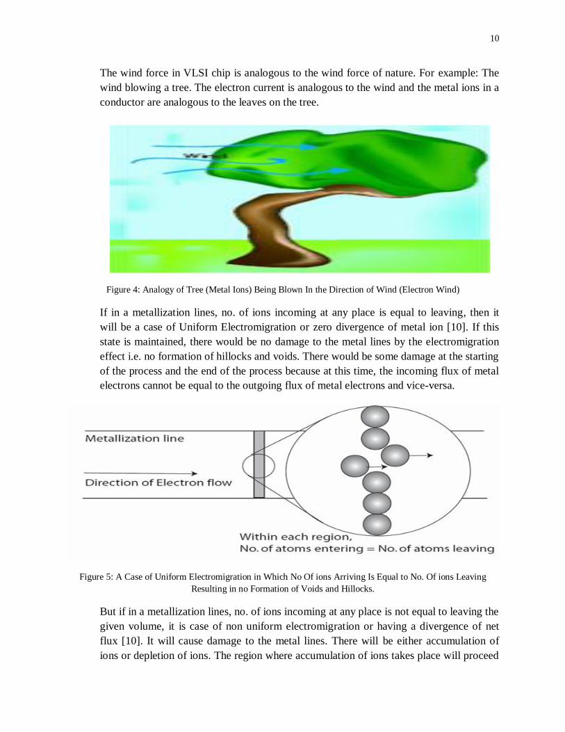
The wind force in VLSI chip is analogous to the wind force of nature. For example: The
wind blowing a tree. The electron current is analogous to the wind and the metal ions in a
conductor are analogous to the leaves on the tree.
Figure 4: Analogy of Tree (Metal Ions) Being Blown In the Direction of Wind (Electron Wind)
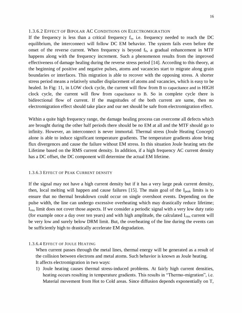
If in a metallization lines, no. of ions incoming at any place is equal to leaving, then it
will be a case of Uniform Electromigration or zero divergence of metal ion [10]. If this
state is maintained, there would be no damage to the metal lines by the electromigration
effect i.e. no formation of hillocks and voids. There would be some damage at the starting
of the process and the end of the process because at this time, the incoming flux of metal
electrons cannot be equal to the outgoing flux of metal electrons and vice-versa.
Figure 5: A Case of Uniform Electromigration in Which No Of ions Arriving Is Equal to No. Of ions Leaving
Resulting in no Formation of Voids and Hillocks.
But if in a metallization lines, no. of ions incoming at any place is not equal to leaving the
given volume, it is case of non uniform electromigration or having a divergence of net
flux [10]. It will cause damage to the metal lines. There will be either accumulation of
ions or depletion of ions. The region where accumulation of ions takes place will proceed

11
by formation of hillocks and the region where depletion of ions takes place will proceed
by formation of voids. Hillocks and Whiskers shown in Fig: 6
As above stated, the polycrystalline material is made up of grains. The ions at the grain
boundary are weakly attached as compared to the ions which are in the centre of grains.
When the electron acceleration is reached to a certain limit, then the momentum
transferred by these electrons to the grain is sufficient to de-attach these weakly attached
atoms. These ions are separated from the grains and will known help in de-attachment of
other ions as they will also transfer their momentum to other weakly attached ions in
other grain.
Figure 6: Hillocks And Whiskers (Right Image) Are Formed Due Accumulation Of Ions .Voids Are Formed Due To
The Depletion Of Ions In That Region. (Left Image)
1.3.3 MICRO STRUCTURAL VARIATION OF METAL WIRES AFFECTING ELECTROMIGRATION
1.3.3.1 EFFECT OF TRIPLE POINT STRUCTURE ON ELECTROMIGRATION
As we know that, practically, the metals are polycrystalline, having grains as their
fundamental repetitive unit. The common point meeting of three grains is known as triple
point. This is the point where the maximum accumulation of ions i.e. formation of hillock
or maximum depletion of ions i.e. formation of voids took place.

12
Figure 7: Triple Points Exists When Three Grains Of Polycrystalline Material Meets
Figure 8: When The Triple Point Structure Is Such That There Are More Paths For Outgoing Rather Than Incoming
(Left Image), Then Void Is Formed. If There Are More Incoming Paths, Rather Than Outgoing (Right Image), Then
Hillock Is Formed.
1.3.3.2 EFFECT OF DIFFERENCE IN GRAIN SIZE ON ELECTROMIGRATION
Polycrystalline material having a fine-grained region has more grain boundaries than a coarse-
grained region, for atomic migration. When the atoms migrate from a fine-grained region to a
Figure 9: When The Atoms Moves From Fine-Grained Region To Coarse Grain Region, Hillocks Are Formed And
When The Atoms Moves From Coarse Grain Region To To Fine-Grained Region, Voids Are Formed.

13
coarser grain region then by the process of accumulation of atoms hillocks are formed . When
the atoms migrate from a coarse-grained region to a fine grained region, then by the process of
depletion of atoms, voids are formed.
1.3.4 PROPERTIES OF DIFFERENT METAL INTERCONNECT AND THEIR EFFECT ON
ELECTROMIGRATION
For a metal to act as ideal interconnect it should have low resistivity, a high mechanical stability,
a good adherence and low stress. It should be easy to etch for pattern generation. It should be
stable throughout processing including at dry and wet oxidation, passivation and metallization. It
should have low electromigration for use in window contacts. It should be stable in oxidation
ambient and should form a stable oxide.
From all the metals available, only four metals are there which has significantly low resistivity
and therefore could be used in VLSI design of metal wires. These include Silver having
resistivity of 1.60 μΩ−cm, Copper having resistivity of 1.67 μΩ−cm, Gold of resistivity of 2.3
μΩ−cm and Aluminum having resistivity of 2.69 μΩ−cm. All the resistivity data are at 293 K.
The most widely used interconnection material previously was Aluminum, despite having a low
conductivity in comparison with other materials such as silver, copper and gold having high
conductivity values. This was because of the following reasons:
1) Silver (Ag) easily gets oxidized, due to which its conductivity decreases. So it could not
maintain its high conductivity with device life time.
2) Copper (Cu) also gets oxidized easily resulting into the sharp decrease in conductivity of
the material.
3) The deposition of Silver (Ag) and Gold (Au) as a very low resistance films is also very
difficult.
Aluminum has high conductivity and it can be easily deposited over silicon. Aluminum forms a
protective layer Al2O3 oxide layer over silicon, which prevents further oxidation due to which
the conductivity does not further, deteriorates. Due to these properties, aluminum was the most
sought element used for the preparation of metal contacts in initial period of VLSI design.
But know a day‟s copper is being used in industry replacing aluminum and various alloys
because of following advantages:
1) Cu is more conductive than Al and Au but is only slightly worse than Ag, thus we can
decrease the width size of the metal line for the same resistance as in copper. Thus we
have lower resistive losses (ρCu = 1.67 μΩ cm, ρAl = 1.65 μΩ cm). Al is approximately
60% more resistive than Pure Cu.
2) Al is more prone to electromigration phenomenon due to which there is rapid formation
of hillocks and voids, while Copper is less prone to this phenomenon due the higher mass
of atoms and a higher melting point. In aluminum, migration of atoms is along grain

14
boundaries and surfaces but there is negligible bulk transport in Copper. (Bulk self
diffusivity of Cu: 1.8×10⁻¹⁶
m2 s
-1 and Bulk self diffusivity of Al: 1.9×10
-12 m
2 s
-1 at
933 K). It is one of the most important properties due to which we have moved toward
copper metal wire [5].
But there are disadvantage of copper metal lines:
1) Copper has tendency to diffuse rapidly into Si and Si-oxide, causing defects such as
deep-level defects which contaminates the Si at the metal contact between metal and
substrate.
2) In copper, the electromigration damage is at the top surface of metal wire as the top metal
wire is the main transport path. The integrated circuit having Aluminium -based wire
metallization does not have electromigration damage at the top surface of metal wire. The
Aluminium forms a protective oxide layer which prevents it from surface transport of
atoms [5][11][12][13].
1.3.5 METHODS TO REDUCE ELECTROMIGRATION IN METAL WIRES
1) We should always took the width of metal lines such that they are able to carry the
minimum current given by EM current limits (Idc) in Design Rule Manual (DRM) which
are generated by considering 0.1% product failure over 10 years at 125°C.
2) We could diverge the excess current, by providing a parallel or alternative metal line such
that the current flowing from both is less than the EM current limits (Idc).
3) We should design the metal structures such that the narrow layers are deposited and
annealed in such a manner that all the grains run perpendicular to the track. These are
known as Bamboo structures [5]. In bamboo structures, the rectangular holes are slotted
inside the metal line so that the individual metal width is less than the average grain size
whereas the overall resultant metal width is sufficient for power requirements. So there
are no disordered grain boundaries in the path of flow of electrons, so no
electromigration.
Figure 10: A Metal Lines in Which Grains Are Perpendicular To The Track. As The Flowing Electron Does Not
Find The Disordered Grain Boundaries, There Is No Electromigration.
1.3.6 EFFECT OF DIFFERENT CURRENT SIGNAL ON ELECTROMIGRATION
A signal can be of different nature i.e. Unipolar Pulsed DC, Bipolar AC and peak current. There
response to the electromigration is also different. So we have to analyze each one.
1.3.6.1 UNIPOLAR PULSED DC ON ELECTROMIGRATION

15
When we are applying a very high frequency signal, particularly, if the frequency is higher than
the jumping frequency of a vacancy, neither can the system respond to the current change
dynamically, nor can vacancies setup DC equilibrium in such a short period. Atoms cannot react
to on and off periods and only feel an average current density. But when the width of pulses is
long (means the frequency is very low), vacancies can reach to their DC equilibrium, and an
atomic gradient is built up during the on-time period [14]. During the current-off period such
atomic gradients can bring relaxation. However if the structure is much longer then Blech length
[18][19][20], this relaxation is insignificant compared to EM stress. So if the length of the metal
wire is less the Blech length, then we can increase the current carrying limit of the metal segment
for same electromigration violation. In Fig: 11, in LOW clock cycle, the current will flow from
the drain of M1 to B and in HIGH clock cycle, there is no current flow through this net. So in
complete cycle there is unidirectional flow of current. So degradation of nets will be through
unidirectional current pulse in these types of nets.
FIGURE 11: Circuit Showing Net Connecting B and Cload Will Be Affected From Bidirectional Current. Nets
Connecting B And Drain Of M1 And B And Source Of M2 Will Be Affected From Unidirectional Current.
Same case also applies for the net joining point B and drain of M2. In this net, in HIGH clock
cycle, the current will flow from B to the drain of M2 and in LOW clock cycle, there is no
current flow through this net. So in complete cycle there is unidirectional flow of current. So
degradation of nets will be through unidirectional current pulse.
16
1.3.6.2 EFFECT OF BIPOLAR AC CONDITIONS ON ELECTROMIGRATION
If the frequency is less than a critical frequency fo, i.e. frequency needed to reach the DC
equilibrium, the interconnect will follow DC EM behavior. The system fails even before the
onset of the reverse current. When frequency is beyond f0, a gradual enhancement in MTF
happens along with the frequency increment. Such a phenomenon results from the improved
effectiveness of damage healing during the reverse stress period [14]. According to this theory, at
the beginning of positive and negative pulses, atoms and vacancies start to migrate along grain
boundaries or interfaces. This migration is able to recover with the opposing stress. A shorter
stress period means a relatively smaller displacement of atoms and vacancies, which is easy to be
healed. In Fig: 11, in LOW clock cycle, the current will flow from B to capacitance and in HIGH
clock cycle, the current will flow from capacitance to B. So in complete cycle there is
bidirectional flow of current. If the magnitudes of the both current are same, then no
electromigration effect should take place and our net should be safe from electromigration effect.
Within a quite high frequency range, the damage healing process can overcome all defects which
are brought during the other half periods there should be no EM at all and the MTF should go to
infinity. However, an interconnect is never immortal. Thermal stress (Joule Heating Concept)
alone is able to induce significant temperature gradients. The temperature gradients alone bring
flux divergences and cause the failure without EM stress. In this situation Joule heating sets the
Lifetime based on the RMS current density. In addition, if a high frequency AC current density
has a DC offset, the DC component will determine the actual EM lifetime.
1.3.6.3 EFFECT OF PEAK CURRENT DENSITY
If the signal may not have a high current density but if it has a very large peak current density,
then, local melting will happen and cause failures [15]. The main goal of the Ipeak limits is to
ensure that no thermal breakdown could occur on single overshoot events. Depending on the
pulse width, the line can undergo excessive overheating which may drastically reduce lifetime;
Irms limit does not cover those aspects. If we consider a periodic signal with a very low duty ratio
(for example once a day over ten years) and with high amplitude, the calculated Irms current will
be very low and surely below DRM limit. But, the overheating of the line during the events can
be sufficiently high to drastically accelerate EM degradation.
1.3.6.4 EFFECT OF JOULE HEATING
When current passes through the metal lines, thermal energy will be generated as a result of
the collision between electrons and metal atoms. Such behavior is known as Joule heating.
It affects electromigration in two ways:
1) Joule heating causes thermal stress-induced problems. At fairly high current densities,
heating occurs resulting in temperature gradients. This results in “Thermo-migration”, i.e.
Material movement from Hot to Cold areas. Since diffusion depends exponentially on T,

17
thermal gradients can cause significant atomic flux divergences, meaning the depletion of
metal atoms and appearance of hillocks.
2) Joule Heating will also increase the ambient temperature, thus exaggerating
Electromigration.
Black‟s law cannot be used to extract the lifetime under real working conditions
accurately until joule heating effects are minimized.
1.4 METHODS USED FOR CALCULATION OF ELECTROMIGRATION
There are various methods used for the calculation of electromigration. The pioneer work
include of the Blech and the method which is utilized in today‟s industry known as
standard/Golden methodology.
1.4.1 BLECH METHOD FOR CALCULATION OF ELECTROMIGRATION FAILURE
Blech, in 1969 [2] gives the method to calculate the mean time to failure [MTTF]. It was a
classical extrapolation model [16] given by
MTTF =Abj-n
exp(Ea/KT)
Where
n= current density exponent which depend on diffusion process.
Ea = Activation energy of dominant diffusion mechanism in interconnect i.e. nucleation-
dominated and growth-dominated failures.
K = Boltzmann constant.
T= temperature in Kelvin.
In this method, the accurate values of n and Ea needs to be calculated. If n varies from over
the common range of 1 to 2, the extrapolated lifetime changes by 45 times as it varies with
the inverse exponential power of current density. The magnitude of current density is very
much less than 1.
1.4.2 STANDARD /GOLDEN METHOD USED IN INDUSTRY
This method is employed presently in Electromigration violation testing in industry. The
reliability of a memory means that memory would be from any functional error for say at least
10 years at the costumers‟ environment but it is infeasible to wait for let‟s say, 10 years to see
characteristics and reliability of memory. So to avoid this, we accelerate the process properties
such as operating voltage, temperature and frequency which wear out the Memory. Then from
this accelerated experimental data, we can extrapolate the life time/ reliability of the memory at
the nominal condition through reliability prediction model. In particular, target applications are
assumed to specify a cumulative failure of 0.1% product failure after 10 years cumulative
operating period at junction temperatures of 125°C. This target is an umbrella specification
designed to cover all the various profiles. Proposed EM current limits (Idc) in Design Rule
Manual (DRM) are generated by considering 0.1% product failure over 10 years at 125°

18
CHAPTER 2: MOTIVATION AND OBJECTIVE
2.1 MOTIVATION
With the advancement in technology , the transistor size as well as the metal wire‟s width (w)
which links them, is being reduced but the current (I) which flows through the devices and the
interconnect is not reduced in that proportion. So current density (J= I/AREA) has increased.
This results in the electromigration effect which can fail our Integrated circuit (IC). The
possibility of failure of IC by electromigration effect will kept increasing as the current density
in integrated circuit will be kept increasing with advancement in technology. The problem of
electromigration is also addressed in International Technology road map for
semiconductor (ITRS), Interconnect 2011 [17] and regarded as a major cause of failure of
VLSI chips.
The VLSI semiconductor industries must verify their integrated circuit before going on silicon
whether it is electromigration free or not. So in the fabrication of IC, another step has to be
included to validate that the nets in VLSI chips are electromigration violation free or not. To test
the Electromigration violation of let say, 1024 x 64m4 SRAM memory chip of
ST_SPHD_LOLEAK compiler, it takes 270 min. The effect of including this step will result in
more time in tapping out this IC as some time will also be elapsed for electromigration test.
For the verification of electromigration test, we have to require some tools like Calibre from
Metorgraphics and star RCXT from Synopsys for extraction of capacitances, XA from Synopsys
for calculation of resistance of segment and current carried by metal wire and then Totem from
apache, is used for analyzing whether electromigration rule in nets of memory instance is
violated or not. The dependency on these tools to calculate the electromigration, increases the
financial burden on the VLSI industry and at the end, it increases the cost of manufacturing of
IC. This will also attract the need of extra human resource, to operate these tools for the
verification of Electromigration.
We can conclude that by including step of verification Of Electromigration Test in the
fabrication of VLSI CHIPS will result in increase of time period in delivery of chip and extra
financial burden on the industry for buying tools and for paying human resource.
2.2 OBJECTIVE
The verification of electromigration violation test during the fabrication of VLSI chip is known a
must condition, particularly in SRAM memories. Therefore, we have to introduce a novel
methodology which should take minimum time and should have least dependency on tools.

19
CHAPTER 3: STANDARD /GOLDEN METHOD USED FOR ELECTROMIGRATION
CALCULATION
In today‟s VLSI industry, to validate the electromigration test of SRAM memories, there is a
standard and a stable method of three steps having input as the gds, cdl and technology file of the
memory instance. The three steps are: 1) capacitance extraction of devices and metal
interconnects 2) equivalent resistance extraction and current estimation in the metal segment 3)
Electromigration calculation and generation of electromigration result data. We have verified
these steps by using tools such as Calibre from Metorgraphics and star RCXT from Synopsys
for extraction of capacitances, XA from Synopsys for calculation of resistance of segment and
current carried by metal wire and then Totem from apache is used for analyzing whether
electromigration rule is violated or not. Here we will be demonstrating each step by using the
circuit in fig 12. This circuit can be considered to be analogous to the circuits in memory cut
instance. So the steps which we are utilizing to calculate the electromigration in net BC of this
circuit are exactly same as we do while calculating the electromigration of a memory cut. The
only difference would be that this circuit is small but memory cut would be large.
Figure 12: The Inverter (Left) Is Driving The Other Two Circuit (Right And Middle). So We Can Model The Other
Two Inverter As The Load Of First (Left) Inverter Using Equivalent Resistance (Requivalent) And Capacitance
(Cequivalent).

20
3.1 DETAILED ANALYSIS OF STANDARD METHOD USED FOR ELECTROMIGRATION
We give the gds, cdl and technology file of the memory instance as the input. The GDS file
consists of all the metal layers and other supporting layer which are helpful in designing of
mosfet or overall circuit. The layer‟s widths, spacing with other layer which are adjacent and
side way or any property of layer are according to the technology file. In Fig: 13 the green
rectangular line shows the power line at upper level feeding the blue metal lines at lower
hierarchy which are feeding power to the mosfet. The green layer shows mosfet substrate space
and red layer shows the path of gate‟s silicon oxide. The light brown dotted layer represent that if
there is any mosfet present in this layer, it should be PMOS. So gds file only consist of layers or
boundaries of different colors which represent the metal line or signify any property representing
the mosfet or overall circuit but how these metal lines are connected with each other is described
in CDL file. So we can say that combination of CDL file, GDS file and technology file of a
circuit is a complete representation of and VLSI circuit or SRAM memory.
Figure 13: Gds of Inverter In 65 nm
3.1.1 CAPACITANCE EXTRACTION
We apply the capacitance extraction process at the FuncCmax mode in which Capacitance is
maximum and resistances is minimum, at the maximum temperature (125oC), so that we get the
most optimistic Electromigration Violation data and are extracting the capacitance of all nets and
devices. Here the capacitance is extracted in two processes.
3.1.1.1 CAPACITANCE EXTRACTION OF DEVICES

21
In the memory instance, first the devices and there connectivity with the metal line is checked by
the device extractor tool. We have used Calibre from metorgraphics for this purpose. It provides
a database in which the device recognition is made and the design network is established, and on
which the Interconnect Extractor tool will be used. For the Fig: 12, the calibre will recognize the
M1, M3 and M5 as NMOS and M2, M4 and M6 as PMOS. It will also generate the data that
which metal line is connected with the drain, source and gate of MOSFET and will store this
data.
3.1.1.2 CAPACITANCE EXTRACTION OF METAL LINES
For the extraction of capacitance of the metal lines, the Interconnect Extractor tool is used
which utilizes the database of the Device Extractor LVS to extract the RC parasitics on the
interconnect layers and to generate the suitable spice netlist. We have used star RCXT tool from
synopsys as an interconnect extractor. For the schematic in fig 11, the tool will calculate the
capacitance of metal segment GH (CGH) , BH (CBH ), BC (CBC ), CD (CCD ) ,CE (CCE) , CF (CEF),
DQ (CDQ) , DN (CDN) , FL (CFL), FK (CFK) and generate the equivalent capacitance‟s including
the capacitance from interaction of MOSFET and metal wire, if they are present. Here we are
neglecting the capacitance between the metal line and the ground. So we can represent the
equivalent capacitive load of net BC by the capacitance Cequivalent having the equivalent
capacitance of CBC , CCD, CEF, CCE, CDQ, CDN, CFL and CFK. This is shown in Fig: 14.
Figure 14: The Equivalent Circuit for the Nets BC, CD, EF, CE, DQ, DN, FL, FK. There Equivalent Capacitance Is
Termed As Cequivalent And Equivalent Resistance Is Termed As Requivalent. The Current Flowing Bc Is Termed
As Current Source I (BC)
3.1.2 EQUIVALENT RESISTANCE EXTRACTION AND ESTIMATION OF CURRENT
3.1.2.1 ESTIMATION OF CURRENT
The XA tool from synopsys is used for the estimation of current. It will do post layout simulation
and we will be having the current flowing in the each net of circuit. This current flowing in each
net of circuit will act as the current source. Let the current flowing in the net BC of circuit shown

22
in Fig: 10 I(BC). So this current will act as the current source for the circuit which are load to
this Net.
3.1.2.2 CALCULATION OF EQUIVALENT RESISTANCE EXTRACTION
To extract the equivalent resistance of all the nets of a memory instance, we are using xa tools
from synopsys. The tool will calculate the resistance of each net. For the schematic in fig 11, the
tool will calculate the resistance of metal segment GH (RGH) , BH (RBH ), BC (RBC ),CD (RCD ) ,
CE (RCE) , CF (REF), DQ (RDQ) , DN (RDN) , FL (RFL), FK (RFK) and generate the equivalent
Resistance including the resistance of MOSFET , if they are present. So we have the equivalent
resistance shown in Fig: 14.
3.1.3 ELECTROMIGRATION CALCULATION
The totem tool from apache is used for the calculation of Electromigration violation data. It
compares the current. It contains a database of I (Carried) of each net which is obtained
subtracting the drop by equivalent resistance and equivalent capacitance. It compares the ICarried
with the current limits (Idc) in Design Rule Manual (DRM) which is generated by considering
0.1% product failure over 10 years at 125°C. The Net is said to be Electromigration violated if
the ratio of Icarried/ Idc > 1. The Idc is different for different metal width line and is also
temperature and frequency. So a net could be electromigration violated at one combination of
temperature and frequency and at other combination it may not.
3.2 ADVANTAGES
1) It is one of the stable and most reliable method for the verification electromigration
violated Nets
2) This is most accurate method. So it is considered as the standard method for
electromigration test.
3.3 LIMITATION
1) This method takes a huge time. So it account to some considerable delay in tapping out of
the SRAM memory.
2) This method requires four tools, so it increases the financial burden on the industry, due
to which the cost of fabrication of IC increases.

23
CHAPTER 4: PROPOSED METHODOLOGY FOR CALCULATION OF
ELECTROMIGRATION OF SIGNAL NETS
4.1 INTRODUCTION
Our methodology is based on the data analysis and memory based Electromigration compliance
estimation. In this methodology, we will be analyzing and requiring the electromigration
database of the three memory instances of same memory compiler i.e. 1) Memory instance
having highest no. rows and lowest no. of columns. 2) Memory instance having lowest no. rows
and highest no. of columns. 3) Memory instance having lowest no. rows and lowest no. of
columns. This electromigration database would be generated from the previous standard method
discussed in chapter 3. So by using the database of these three memories instance, we can
generate the electromigration data of memory instance of any configuration i.e. any no. of rows
or any no. of column but of same compiler, without using any tool. In this methodology, we are
modeling the electromigration of each net by analyzing and using the data of three memory
instances explained above.
** Here rows means number of words divided by the input of multiplexer and columns means
the no of output bits multiplied by the input of multiplexer. Ex: If suppose we have memory
instance of name 2048 X 64m4, it means that we are using the multiplexer of 4 to 1 having two
select lines. The 64 signify the no. of output bits in memory instances. It will be having 64x4 =
256 columns. The 2048 means the no. of words and it will have 2048/4 = 512 rows. This means
this memory instance will be having 512 word lines and one word line will be attached to 256
memory cells or we can say that 1 word lime will be attached to 256 columns.
***The word „NET‟ means a metal line which is connecting two devices. Devices could be
metal lines as well as MOSFET.
****The word „load‟ signifies the equivalent capacitance of the circuit which is at the output of a
driver.
4.2 DIFFERENT TYPES OF NETS IN LAYOUT
Nets in the memory layout are classified broadly in two categories depending on the type of
current they carry: Power Nets and Signal nets. The signal nets are further classified in two
types:-
1) Power Nets: These nets carry the power. These nets are bidirectional on same level i.e.
the same net will lying in horizontal as well as in well vertical direction. Examples of
these nets are Vddma Net, Gndm Net or Vddmp Net.
2) Signal nets: These nets carry the different type of signals such as dummy bit read,
dummy bit write, Output signal, input signals, various clocking signal. These nets either

24
vary in horizontal direction or in vertical direction but not in both directions. The signal
nets are further classified as global nets and Local Nets.
A) Global net: Global net are the nets which stretches from one block to another. Global
nets can be further classified in two categories based on the manner they are designed
in the layout:-
I. Horizontally lying signal nets: These are the nets whose length varies with the
variation in no. of bits. There size of these nets remains constant if the no. of
rows is varying. In figure: 16, DWL net is the horizontally lying signal net.
II. Vertically lying signal nets: These are the nets whose length varies with the
variation in no. of rows. There size of these remains constant if the no. of bits
is varying. In figure: 16, DBL net is the horizontally lying signal net.
B) Local net: Local nets are those nets which are confirmed locally. They are found in
control block. Example of such types of nets is sleepbmp net in control block.
4.3 ARCHITECTURE OF SRAMS AND RESPONSE OF NETS IN BLOCKS TOWARD THE
ELECTROMIGRATION
SRAM memories have typically 4 sub blocks i.e. controlling block, input / output block, row
decoder block and core block.
1) Control Block: It is the block which generates the clocking and other synchronizing
signal for various purposes. It also receives the address bit which propagates later to the
row decoder after latching with other signals such as clocking signal. If there are two
memory instances such as 2048x144m4 and 1660x64m4 of same compiler, then this
block remain same in both memory instance. We can also conclude that the load provided
by net which is in this block will be same in all memory instances irrespective of the size
of the memory instance. So, we can say that the electromigration effect generated in this
net of control block will be same for all memory instances of same compiler.
2) Input /output Block: This block has input and output pins and has drivers for that
purposes. As the size of this block increases, the load of the horizontal lying nets in
layout will increase, due to which the current flowing in them will also increase. So the
electromigration in these horizontal lying nets will vary according to the size of
input/output block. The vertical lying nets will have no variation while we are varying the
size of Input /Output block.
3) Row decoder Block: This block has the word line driver of all the rows. The horizontal
size of this block is same irrespective of the size of the memory instance if they are from
the same memory compiler. So a horizontal lying net in all memory instances will
experience same load due to the row decoder block. For a vertical lying net in layout if

25
rows are increasing, the load on net will increase, so the electromigration will also
increase.
Figure 15: Architecture of SRAM Memories
4) Core: The core consists of memory cells in which the data gets stored. The size of core
varies when we are varying the no. of rows as well as when we are varying the no. of
columns. As the no. of rows increases, the load of the vertical lying nets in layout will
also increase, due to which the current flowing in them will be increasing. So the
electromigration in these vertically lying nets depending on the no. of rows. Similarly, the
Electromigration of horizontal lying nets will depend on the variation of no. of bits in the
memory instance.
4.4 PROPERTIES OF NETS WHICH MAKE THIS METHODOLOGY FEASIBLE
We have utilized the properties of the nets of SRAMs in the way they are designed in layout.
1) For a compiler, the architecture of the all memory instance will be same. The architecture
does not depend upon the no. of bits or no. of columns. So if there are two memory
instances such as 2048x144m4 and 1660x64m4 of same compiler, then both will be
having control blocks and row decoder in the middle and core and input /output block in
both side of control and row decoder. The sized of the memory instance could be
different but the basic building blocks will be same. It concludes that same type of nets
will be there but length of nets could differ. Example in 2048x144m4, the output nets
would be 144 but in 1660x64m4, the output nets would be 64 only but output nets are

26
there having same properties. Also, the length of a global signal net would be more in
2048x144m4 than 1660x64m4.
2) For a compiler, the control block is same for all the memory instances. We can also
conclude that the load provided by nets in this block will be same irrespective of the size
of the memory instance. So, we can say that the electromigration effect generated in the
nets of control block will be same for all memory instances of same compiler.
3) Signal nets have mutual exclusive impact while varying no. of core cells and row decoder
(row) or varying no. of bits (column). It means if horizontally lying nets in layout are
changing EM by varying no. of bits; it will not vary its EM if we are varying no. of core
cells and row decoder. Similarly, if vertically lying nets in layout are changing EM by
varying no. of core cells and row decoder, it will not vary its EM if we are varying no. of
bits. So we can conclude that either a net will not have any impact on the variation of size
of memory, ex. Local Nets otherwise the net will vary its EM in only one case of
variation in no. of bits or variation in no. of rows.
4.5 EFFECT ON ELECTROMIGRATION DUE TO THE VARIATION OF NO. OF ROWS
AND COLUMNS
A net in all memory instances originates from a single source as the architecture of all memory
instances is same if they are generated from the same compiler. The layout of SRAM memories
consist of Local Nets and Global nets. The Local nets are confirmed in the control block and the
variation in the electromigration in these nets does not depend on the variation of no. of rows and
columns. Global net are the nets which stretches from one block to another. Global nets are
further divided into Horizontal and vertical nets. The Load (equivalent capacitance) on the
horizontal nets increases with the increase in no. of bits. Similarly, The Load (equivalent
capacitance) on the vertical nets increases with the increase in no. of rows. The current carried
by the nets varies in direct proportion to the load (equivalent capacitance) according to the
following mathematical equation:
A net is said to be electromigration test violated when the ratio of and is greater
than 1. is defined as current limits in Design Rule Manual (DRM) which are generated by
considering 0.1% product failure over 10 years at 125°C .
4.6 MODELING OF SIGNAL ELECTROMIGRATION
As we have discussed earlier, the layout of SRAM memories consist of three types of signal nets:
Local nets, horizontal lying signal nets and vertical lying signal nets. We will be discussing each
one in detail.
1) Local Nets: Local nets are those nets which are confirmed to the control block. The
length of these nets is same in all the memory instances if they are generated from the

27
same compiler. As the equivalent capacitance and the resistance of these net are same in
all memory instances, so the current carried is same for all the memory instances
as the current varies in direct proportion to the capacitance. So the Electromigration of
these nets would also be same for all memory instances.
Suppose we have an electromigration database of two memory cut i.e. 2048x144m4 and
1024x80m4 and we want to find the EM database of local net in memory instance, say
1600x120m4. As we know that the EM of a local net does not depend on the size of
memory instance, so EM of that local net in 2048x144m4 and 1024x80m4 will be same
and we could assume the same EM database for the local net in 1600x120m4.
2) Vertically Lying Global Signal Nets: These are the nets whose length changes with the
change in no. of rows but the length is independent of the no. of bits. Let‟s take an
example of DBL net shown in fig: 16 which is vertically laying global signal net. It
stretches from core to input/output block. The equivalent capacitance of this net
comprises of capacitance from input/output block and core.
So first discuss when the net is in the input/output block. The length of such type of net in
input /output block of all memory instances is same, for the same compiler. So the
equivalent capacitance will also be same. Therefore, the current flowing in this net for all
memory instances will be equal as current carried ( ) by a net is in direct
proportion to the capacitance of net. So we termed this constant current, carried by the
net in input/ output block as „C‟. As the EM is defined as the ratio of and .
Being the as a constant, so normalized EM will be equal to . So normalized
EM contributed by the net when it is in input/output block is „C‟.
Figure 16: Variation of ICARRIED /ILIMIT (Along Y Axis) With Respect To The Variation In No. Rows for
Dbl Net
0
0.5
1
1.5
2
2.5
3
3.5
4
32 1200 2048 (No. of
rows)
EM Violation of a DBL net varying with rows
EM Violation of a
DBL net varying with
rows

28
Figure 17: Variation of Icarried /Ilimit (Along Y Axis) With Respect To The Variation In No. Rows For Dbl Net
The other portion is when the net is in core region. In this portion, the net will have
capacitance due to core region. Let suppose the capacitance due to one row be „m‟. Let
there be total „y‟ rows. Therefore, the capacitance exhibited by this net due to all the rows
will be „m*y‟. So the capacitance in this portion of net will be linearly increasing with the
increment in the no. of rows. As the current is in direct proportion to the capacitance, so
the current carried by this net will also vary by term „m*y‟ and as the EM is defined as
the ratio of and . Being the as a constant, so normalized EM will be
equal to . So normalized EM contributed by the net when it is in core block is
„m*y‟.
*we represent normalized EM as EM only.
So mathematically for vertically lying global signal nets, we can have EM from core as
well as input/output block as follows:
Where,
m = capacitance due to one row
y = total no of rows
c = constant EM in net which will exists in all memory instance independent of no. of rows.
0
0.2
0.4
0.6
0.8
1
1.2
64 128 144 N0. of bits
EM violation of DBL net varying with col.
EM violation of DBL
net varying with col.

29
Suppose we have electromigration data for 2048x4m4 and 32x4m4 and want to get the data for
DBL net in 1200x4m4. Let say the EM data of DBL net for 2048x4m4 be 3.5 and for 32x4m4 be
1.2. Putting these values in equation (1), we will be getting to linear equation (2) and (3)
Solving these two for m and c, we will be getting some values m=0.00114 and c=1.163
Then, putting all of m, c and y=1200 values in (1) for 1200x4m4, we got 2.52
So in this way we will be getting the Electromigration data of vertically varying nets in
32x144m4 or any other memory instance in which bits are constant, without using of any tool.
Fig: 16 VARIOUS ELECTROMIGRATION PARAMETER IN LAYOUT
3) Horizontally Lying Global Signal Nets: These are the nets whose length changes with
the change in no. of bits but the size is independent of the no. of rows. Let‟s take an
example of DWL net shown in fig: 16 which is vertically laying global signal net. It
stretches from core to row decoder block. The equivalent capacitance of this net
comprises of capacitance from row decoder block and core.
So let‟s first discuss when the net is in the row decoder block. The length of such type of
net in row decoder block is same in all memory instances, for the same compiler. So the
equivalent capacitance will also be same. Therefore, the current flowing in this net will
be equal to current carried ( ) by a net is in direct proportion to the capacitance of
net. So we termed this constant current, carried by the net in input/ output block as „C1‟.
As the EM is defined as the ratio of and . Being the as a constant, so

30
normalized EM will be equal to . So normalized EM contributed by the net when
it is in row decoder block is „C1‟.
The other portion is when the net is in core region. In this portion, the net will have
capacitance due to core region. Let suppose the capacitance due to one bit be „m1‟. Let
there be total „x‟ rows. Therefore, the capacitance exhibited by this net due to all the rows
will be „m1*x‟. So the capacitance in this portion of net will be linearly increasing with
the increment in the no. of bits. As the current is in direct proportion to the capacitance,
so the current carried by this net will also vary by term „m1*x‟ and as the EM is defined
as the ratio of and . Being the constant, so normalized EM will be
equal to .
*we represent normalized EM as EM only.
So mathematically for vertically lying global signal nets, we can have EM from core as
well as row decoder block as follows:
Where,
m = capacitance due to one bit
x = total no of bits
c1 = constant EM in net which will exists in all memory instance independent of no. of rows.
Suppose we have electromigration data for 32x4m4 and 32x144m4 and want to get the data for
DBL net in 32x60m4. Let say the EM data of DBL net for 32x140m4 be 3.9 and for 32x4m4 be
1.6. Putting these values in equation (1), we will be getting to linear equation (2) and (3)
Solving these two for m1 and c1, we will be getting some values of m and c.
Then, putting all of m, c and x=120 values in (1) we will get the data for 32x60m4.
So in this way we will be getting the Electromigration data of horizontally varying nets in
32x60m4 or any other memory instance in which rows are constant, without using of any tool.
In above examples, we have used 32x144m4, 2048 x4m4 and 32x4m4 EM database. By
using the database of these, we could get the EM data base of any cut having any no. of
rows and any no. of columns but all should be from same compiler.

31
4.8 PRECAUTION TO BE TAKEN BEFORE IMPLEMENTING THE METHODOLOGY:
1) There should not be any default option on tools while we are taking the EM database of three
cuts through standard method. If suppose the default option is selected, then the tool can switch
to fast operation mode when the memory instance size is large and switches to accurate mode
when the memory instance size is small.
2) Always check that the architecture of the all the memory instance is same or not. If there is
any anomaly then change the memory instance.

32
CHAPTER 5: COMPARISON RESULTS
The electromigration effect is due to three types of current i.e. Unidirectional DC current,
Bidirectional current and peak current. We have analyzed for unidirectional dc current in terms
of I (avg.) and Bidirectional current in terms of I(rms) current.
Memory Cut Total Time by standard
methodology
Total time by our
methodology
Worst Accuracy
of our
methodology wrt
standard for a net
1200x128m4 192 mins 10 sec 4.3 %
2048x130m4 340 mins 10sec 4.8 %
Table 1: Result Of Memory Instance 1200x128m4 And 2048x130m4 for Unidirectional Dc
Current
So for Unidirectional DC current, we can see that for memory instance 1200x128m4, we are
getting our result faster by 1152 times within worst accuracy of 4.3% and for 2048x13m4 cut ,
we are getting the result faster by 2160 times within the worst accuracy of 4.8%.
Memory Cut Total Time by standard
methodology
Total time by our
methodology
Worst Accuracy
of our
methodology wrt
standard for a net
1200x128m4 192 mins 10 sec 1.2 %
2048x130m4 340 mins 10sec 1.3%
Table 2: Result Of Memory Instance 1200x128m4 And 2048x130m4 for Bidirectional Current
So for Bidirectional current, we can see that for memory instance 1200x128m4, we are getting
our result faster by 1152 times within worst accuracy of 1.2% and for 2048x13m4 cut , we are
getting the result faster by 2160 times within the worst accuracy of 1.3%.

33
CHAPTER 6: CONCLUSION AND FUTURE WORK
6.1 CONCLUSION
We have discovered and utilized the property with which EM of nets will either not vary and
if varies then it will vary with rows and columns and prepared a methodology which is very
fast and its accuracy is also comparable that of the standard process, so that EM test could be
verified fast, have less financial burden i.e. require tools for only three times for each
compiler and is least complex.
6.2 FUTURE WORK
6.2.1 MODELING OF POWER NETS
Power nets are the bidirectional nets unlike signal nets whose EM will either not change or if
changes, it will change with either with the variation of rows or columns. We can disintegrate the
nets into small resistances and then apply our methodology for Vddmp, Vddma or gndm net.
34
CHAPTER 7: BIBLIOGRAPHY
1) Moore, Gordon E. (1965). "Cramming more components onto integrated circuits"
(ftp://download.intel.com/museum/Moores_Law/Articles-Press_Releases/Gordon_Moore
_1965_Article.pdf) (PDF). Electronics Magazine. pp. 4. . Retrieved 2006-11-11.
2) "Excerpts from A Conversation with Gordon Moore: Moore‟s Law"
(ftp://download.intel.com/museum/Moores_Law/Video-Transcripts/Excepts_A_
Conversation_with_Gordon_Moore.pdf) (PDF). Intel Corporation. 2005. Retrieved 2006-
05-02.
3) "1965–“Moore's Law” Predicts the Future of Integrated Circuits"
(http://www.computerhistory.org/semiconductor/timeline/1965-Moore.html).Computer
History Museum. 2007. Retrieved 2009-03-19.
4) “Understand and avoid electromigration (EM) & IR-drop in custom IP blocks.”
http://www.synopsys.com/Tools/Verification/CapsuleModule/CustomSim-RA-wp.pdf
5) A. Scorzoni, C. Caprile, and F. Fantini, “Electromigration in thin-film interconnection
lines: models, methods and results,” in Material Science Reports, New York: Elsevier,
1991, vol. 7, pp. 143–219.
6) D. Young and A. Christou, “Failure mechanism models for electromigration,” in IEEE
Trans. on Reliability, vol. 43(2), pp. 186–192, June 1994.
7) J. R. Black, “Mass transport of aluminum by momentum exchange with conduction
electrons,” Proc. IEEE International Reliability Physics Symposium, pp. 148-159, 1967..
8) L. Ting, J. May, W. Hunter, and J. McPherson, “AC electromigration characterization
and modeling of multilayered interconnects,” Proc. IEEE Int. Reliability Physics
Symposium, 1993.
9) J. M. Towner, E. P. van de Ven, “Aluminum electromigration under pulsed dc
conditions,” Proc. IEEE International Reliability Physics Symposium, pp. 36-39, 1983
10) http://www.doitpoms.ac.uk/tlplib/electromigration/
11) Ch. S. Hau-Riege, “An introduction to Cu electromigration,” in Microel. Reliab.,vol. 44,
pp. 195–205, 2004
12) A.G. Sabnis, “VLSI Reliability,” VLSI Electronics—Microstructure Science, London:
Academic Press Ltd., vol. 22, 1990.
13) B. Li, T. D. Sullivan, T. C. Lee et al., “Reliability challenges for copper interconnect”, n
Microel. Reliab., vol. 44, pp. 365–380, 2004
14) J. A. Maiz, “Characterization of electromigration under bidirectional (BC) and pulsed
unidirectional (PDC) currents,” in Proc. Int. Reliab. Phys. Conf. (IRPS),1989, pp. 220–
228
15) K. Banerjee, A. Amerasekera, N. Cheung et al., “High-current failure model for VLSI
interconnects under short-pulse stress conditions,” in IEEE Electron Device Lett., vol.
18(9), pp. 405–407, Sept. 1997

35
16) J. R. Black, “Electromigration failure models in aluminum metallization for
semiconductor devices,” in Proc. of the IEEE, vol. 57(9), pp. 1587–1594, 1969…Black
formula
17) “ITRS 2011 edition reports.” http://www.itrs.net/Links/2011ITRS/Home2011.htm
18) F. Wei, C. L. Gan, C. V. Thompson et al., “Length effects on the reliability of dual-
damascene Cu interconnects,” in Proc. 2nd Ann. Material Research Soc. Symp., vol. 716,
2002, pp.B13.3.1–B13.3.6.
19) I. A. Blech, “Electromigration in thin aluminum films on titanium nitride,” in J. Appl.
Phys., vol. 47, pp. 1203–1208, 1976.
20) A. V. Vaigar, S. G. Mhaisalkar and A. Krishnamoorthy, “Electromigration behavior of
dual-damascene Cu interconnects – Structure, width, and length dependences,” in
Microel. Reliab., vol. 44, pp. 747–754, 2004.