structure of an al fe ni decagonal quasicrystal …przyrbwn.icm.edu.pl/app/pdf/126/a126z2p53.pdf ·...
TRANSCRIPT
Vol. 126 (2014) ACTA PHYSICA POLONICA A No. 2
Proceedings of the 12th International Conference on Quasicrystals (ICQ12)
Structure of an Al�Fe�Ni Decagonal Quasicrystal Studied by
Cs-Corrected STEM
A. Yasuharaa,∗, K. Yamamotob, K. Yubutac and K. Hiragac
aEM Application Group, EM Business Unit, JEOL Ltd., Tokyo 196-8558, JapanbDepartment of Physics, Nara Women's University, Nara 630-8506, Japan
cInstitute for Materials Research, Tohoku University, Sendai 980-8577, Japan
The structure of an Al�Fe�Ni decagonal quasicrystal with two quasiperiodic planes along the periodic axisin an Al72Ni24Fe4 alloy has been examined by spherical aberration (Cs)-corrected scanning transmission electronmicroscopy with high-angle annular dark-�eld and annular bright-�eld techniques. The transition-metal atoms andmixed sites (MSs) of Al and transition-metal atoms are represented as separated bright dots in the observed high-angle annular dark-�eld scanning transmission electron microscopy images, and consequently the arrangements oftransition-metal atoms and mixed sites on the two quasiperiodic planes can be directly determined. The transition-metal atoms are arranged on a pentagonal tiling of an edge-length of 0.76 nm. The close examination of observedannular bright-�eld- and high-angle annular dark-�eld scanning transmission electron microscopy images indicatesthe existence of large decagonal columnar clusters with 3.2 nm diameter, and their arrangement on pentagonal,thin rhombic and squashed hexagonal tiles with an edge-length of 3.2 nm. The arrangements of transition-metalatoms in these three tiles are placed on an ideal pentagonal tiling with an edge-length of 3.2 nm, which is generatedby the projection of a �ve-dimensional hyper-cubic lattice. The vertices are denoted by 5D hyper-cubic indicesand then they are projected on the occupation domains in perpendicular space. The arrangement of Al atoms aswell as transition-metal atoms and mixed sites in the large decagonal atom cluster with about 3.2 nm diameter isinterpreted from the observed high-angle annular dark-�eld- and annular bright-�eld scanning transmission electronmicroscopy ABF-STEM images.
DOI: 10.12693/APhysPolA.126.637
PACS: 61.66.�f
1. Introduction
Recently, we have extensively re-examined the struc-tures of Al-transition-metal (TM) decagonal quasicrys-tals and their crystalline approximants by Cs-correctedannular bright-�eld (HAADF) scanning transmissionelectron microscopy (STEM) HAADF-STEM, which hasenough resolution to represent individual TM atoms asseparated bright dots in observed images of decagonalquasicrystals. We have proposed new structure mod-els characterized by bond orientational order (BOO)arrangements of TM atoms [1�5] instead of previouscluster-based models that have been widely accepted fora long time.The Al-Ni-Fe decagonal quasicrystal was �rst found in
rapidly solidi�ed alloys [6], and then found as a stablephase in a conventionally solidi�ed Al71Ni24Fe5 alloy [7].This stable decagonal phase is also known to be a highly-ordered one [8, 9].In the present paper, we aim to produce a new inter-
pretation about the structure of this Al-Ni-Fe decagonalquasicrystal by the full use of Cs-corrected STEM withHAADF and annular bright-�eld (ABF) techniques andto obtain an occupation domain for the arrangement ofTM atoms in perpendicular space.
∗corresponding author; e-mail: [email protected]
2. Experimental procedures
An alloy of a nominal composition of Al72Ni24Fe4 wasprepared by melting high-purity (99.99%) metals of Al,Ni and Fe in an arc furnace under Ar atmosphere. The in-got was sealed in an evacuated quartz tube and annealedat 900 ◦C for 40 h HAADF- and ABF-STEM images weresimultaneously taken with the incident beam parallel tothe periodic axis by using a Cs-corrected electron micro-scope (JEM-ARM200F). The STEM images presentedin this paper are �ltered by reconstructing using Fourierdi�ractograms of the original images and apertures sur-rounding di�raction spots in the Fourier di�ractograms,in order to reduce noises in the original images. The com-position of the Al-Ni-Fe decagonal quasicrystal was de-termined by energy dispersive X-ray Spectroscopy (EDS)to be Al71Ni24Fe5, which is similar to the nominal com-position.
3. Experimental result and discussion
Figure 1a is an ABF-STEM image of the Al-Ni-Fedecagonal quasicrystal, and all atomic columns are con-sidered to be represented as separated dark dots along theperiodic axis. In the image, one can see that small ringsformed by ten dark dots are arranged with an intervalabout 0.66 nm. In the arrangement of the ring contrasts,de�nite large clusters formed by ten small rings encirclingwith ten-fold rotational symmetry are observed, as indi-cated by circles. The large clusters are arranged on BOO
(637)

638 A. Yasuhara, K. Yamamoto, K. Yubuta, K. Hiraga
with a bond length of 3.2 nm. Figure 1b is a HAADF-STEM image simultaneously taken with Fig. 1a. Fromthe close examination of bright dots in Fig. 1b, one canrecognize that large decagonal clusters with 3.2 nm di-ameter exist at the positions of the clusters in Fig. 1a andthat they are arranged by edge-shearing and interpene-trating linkages, as indicated by the decagonal frames.
Fig. 1. ABF-STEM (a) and HAADF-STEM (b) im-ages of the Al�Fe�Ni decagonal quasicrystal simultane-ously taken with the incident beam parallel to the pe-riodic axis. Note the large clusters, indicated by circlesin (a), formed by ten small rings encircling with ten-fold rotational symmetry, and a BOO arrangement ofthe decagonal clusters by edge-sharing and interpene-trating linkages with a bond-length of 3.2 nm in (b).
Fig. 2. Enlarged images of a part of Fig. 1b. Mostof the bright dots in the image are connected by twopentagonal tilings with an edge-length of 0.76 nm, asindicated by thin lines in (a) and (b). Note that doublepentagonal arrangements of bright dots, which can beclearly seen in an enlarged image inserted in (a), areobserved in upward pentagonal frames in (a) and in thedownward ones in (b). Large clusters with pentagonalsymmetry, indicated by thick lines, are observed at mostof the vertices of the BOO tiling with an edge-length of3.2 nm.
Figure 2 is an enlarged HAADF-STEM image of a partof Fig. 1b. As indicated by the thin lines in Fig. 2a and b,most of the bright dots in the image can be connectedby two types of pentagonal tilings with a bond-length of0.76 nm. In upward pentagonal frames in the pentago-nal tiling of Fig. 2a and downward ones in Fig. 2b, onecan recognize double pentagonal arrangements, which arecomposed of pairs of bright dots along the directions of�vefold rotational symmetry, as can be clearly seen inan enlarged image inserted in Fig. 2a. From the previ-ous interpretations [1, 3, 5], it can be concluded that all
bright dots connected by lines in Fig. 2a and in Fig. 2bcorrespond to the TM atoms respectively on A and Bquasiperiodic planes stacked along the periodic axis. Fur-thermore, the innermost �ve dots in the double pentago-nal arrangements correspond to the mixed sites (MSs) inthe tiling plane, and the outer �ve dots in these doublepentagonal arrangements are the TM and/or MSs in adi�erent plane. The unevenness of the brightness of thebright dots corresponding to MSs suggests the Al/TMratio being di�erent at every MS position. On the otherhand, the contrast distributions in downward pentagonsin Fig. 2a and in upward ones in Fig. 2b have asymmetricarrangements of bright dots. The positions of bright dotsin the asymmetric arrangements have been interpretedin the previous paper for a decagonal quasicrystal in anAl72Co8Ni20 alloy [5], but they are not mentioned in thepresent paper, because of their inde�nite arrangements.The large clusters with pentagonal symmetry, indicatedby pentagons with thick lines in Fig. 2, are observed atmost of vertices of the BOO tiling with an edge-length of3.2 nm. Those clusters correspond to the decagonal onesin Fig. 1b.From the HAADF-STEM image of Fig. 2, the arrange-
ments of TM atoms and MSs on the A and B planescan be directly derived, as shown in Fig. 3. All the TMatoms and MSs in Fig. 3 are located at the vertices ofa Penrose tiling, a part of which is inserted in Fig. 3a,with an edge-length of 0.25 nm, and consequently theTM atoms and MSs are arranged with BOO. The pen-tagonal arrangements of MSs in pentagonal frames withde�nite directions can be seen in the B plane of the struc-ture of W�(AlCoNi) [1, 10] and τ2-Al3Co [2] crystallinephases, which are considered to be important approxi-mants for the interpretation of Al-TM decagonal qua-sicrystals and in quasiperiodic planes of several types ofAl-Co-Ni decagonal quasicrystals [1, 4, 5].
Fig. 3. Arrangements of TM atoms and MSs in the A(a) and B (b) quasiperiodic planes stacking along theperiodic axis, derived from the arrangements of brightdots in Fig. 2. Note that the pentagonal arrangementsof MSs are located at upward pentagonal frames in (a)and downward ones in (b). All the TM atoms and MSsare located at the vertices of a Penrose tiling, a part ofwhich is inserted in (a), with an edge-length of 0.25 nm.
The TM atoms in squashed hexagonal, thin rhombic,and pentagonal frames with an edge-length of 3.2 nmare placed in an ideal pentagonal tiling of Fig. 4a, which
Structure of an Al�Fe�Ni Decagonal Quasicrystal Studied by Cs-Corrected STEM 639
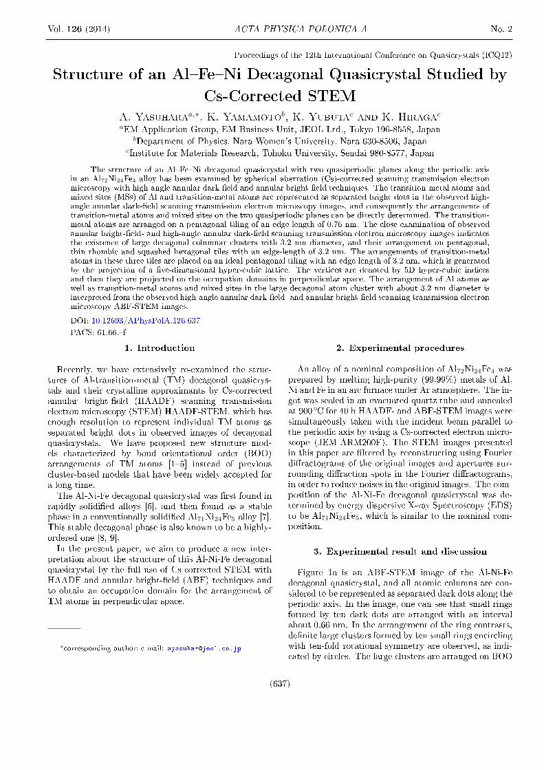
Fig. 4. (a) Ideal pentagonal tiling generated by thewindow (b) in perpendicular space, (c) TM atoms onthe A plane, placed in the ideal pentagonal tiling of (a),and (d); occupation domains of the TM atom positionsof (c). Black circles in (c) are extra TM atoms appear-ing from decagonal symmetry of the occupation domainsof (d). Black and gray star-shaped domains in (d) areproduced from TM atoms in pentagonal frames with op-posite orientations respectively and light gray fat rhom-buses and white thin rhombuses result from TM atomsin thin rhombic and squashed hexagonalframes in (c),respectively.
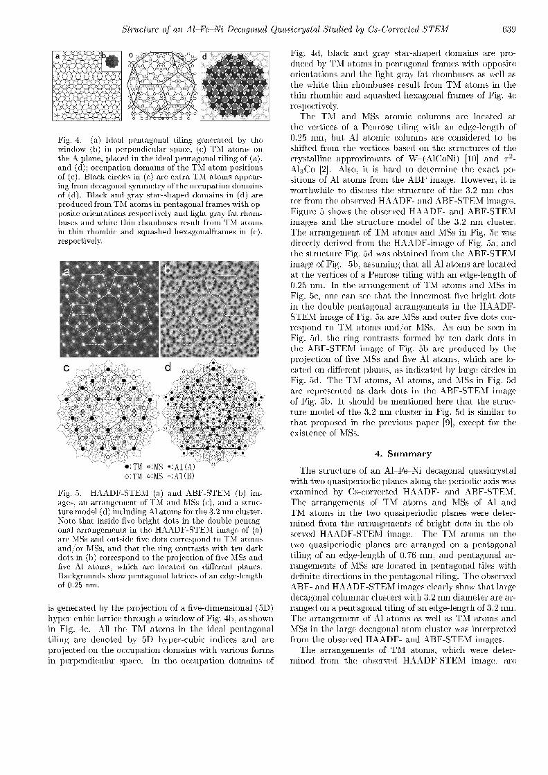
Fig. 5. HAADF-STEM (a) and ABF-STEM (b) im-ages, an arrangement of TM and MSs (c), and a struc-ture model (d) including Al atoms for the 3.2 nm cluster.Note that inside �ve bright dots in the double pentag-onal arrangements in the HAADF-STEM image of (a)are MSs and outside �ve dots correspond to TM atomsand/or MSs, and that the ring contrasts with ten darkdots in (b) correspond to the projection of �ve MSs and�ve Al atoms, which are located on di�erent planes.Backgrounds show pentagonal lattices of an edge-lengthof 0.25 nm.
is generated by the projection of a �ve-dimensional (5D)hyper-cubic lattice through a window of Fig. 4b, as shownin Fig. 4c. All the TM atoms in the ideal pentagonaltiling are denoted by 5D hyper-cubic indices and areprojected on the occupation domains with various formsin perpendicular space. In the occupation domains of
Fig. 4d, black and gray star-shaped domains are pro-duced by TM atoms in pentagonal frames with oppositeorientations and the light gray fat rhombuses as well asthe white thin rhombuses result from TM atoms in thethin rhombic and squashed hexagonal frames of Fig. 4crespectively.The TM and MSs atomic columns are located at
the vertices of a Penrose tiling with an edge-length of0.25 nm, but Al atomic columns are considered to beshifted from the vertices based on the structures of thecrystalline approximants of W�(AlCoNi) [10] and τ2-Al3Co [2]. Also, it is hard to determine the exact po-sitions of Al atoms from the ABF image. However, it isworthwhile to discuss the structure of the 3.2 nm clus-ter from the observed HAADF- and ABF-STEM images.Figure 5 shows the observed HAADF- and ABF-STEMimages and the structure model of the 3.2 nm cluster.The arrangement of TM atoms and MSs in Fig. 5c wasdirectly derived from the HAADF-image of Fig. 5a, andthe structure Fig. 5d was obtained from the ABF-STEMimage of Fig. 5b, assuming that all Al atoms are locatedat the vertices of a Penrose tiling with an edge-length of0.25 nm. In the arrangement of TM atoms and MSs inFig. 5c, one can see that the innermost �ve bright dotsin the double pentagonal arrangements in the HAADF-STEM image of Fig. 5a are MSs and outer �ve dots cor-respond to TM atoms and/or MSs. As can be seen inFig. 5d, the ring contrasts formed by ten dark dots inthe ABF-STEM image of Fig. 5b are produced by theprojection of �ve MSs and �ve Al atoms, which are lo-cated on di�erent planes, as indicated by large circles inFig. 5d. The TM atoms, Al atoms, and MSs in Fig. 5dare represented as dark dots in the ABF-STEM imageof Fig. 5b. It should be mentioned here that the struc-ture model of the 3.2 nm cluster in Fig. 5d is similar tothat proposed in the previous paper [9], except for theexistence of MSs.
4. Summary
The structure of an Al�Fe�Ni decagonal quasicrystalwith two quasiperiodic planes along the periodic axis wasexamined by Cs-corrected HAADF- and ABF-STEM.The arrangements of TM atoms and MSs of Al andTM atoms in the two quasiperiodic planes were deter-mined from the arrangements of bright dots in the ob-served HAADF-STEM image. The TM atoms on thetwo quasiperiodic planes are arranged on a pentagonaltiling of an edge-length of 0.76 nm, and pentagonal ar-rangements of MSs are located in pentagonal tiles withde�nite directions in the pentagonal tiling. The observedABF- and HAADF-STEM images clearly show that largedecagonal columnar clusters with 3.2 nm diameter are ar-ranged on a pentagonal tiling of an edge-length of 3.2 nm.The arrangement of Al atoms as well as TM atoms andMSs in the large decagonal atom cluster was interpretedfrom the observed HAADF- and ABF-STEM images.The arrangements of TM atoms, which were deter-
mined from the observed HAADF-STEM image, are

640 A. Yasuhara, K. Yamamoto, K. Yubuta, K. Hiraga
placed in an ideal pentagonal tiling with an edge-lengthof 3.2 nm, which is generated by the projection of a �ve-dimensional hyper-cubic lattice. All the TM atoms in theideal pentagonal tiling are denoted by 5D hyper-cubic in-dices and are projected on the occupation domains withvarious forms in perpendicular space.
References
[1] A. Yasuhara, K. Saito, K. Hiraga, in: Proc. of Aperi-odic 2012, Eds.: S. Schmid, R.L. Withers, R. Lifshitz,Springer, Berlin 2013, p. 219.
[2] K. Sugiyama, A. Yasuhara, K. Hiraga, in: Ref. [1],p. 237.
[3] K. Yubuta, A. Yasuhara, K. Hiraga, in: Ref. [1],p. 225.
[4] K. Hiraga, A. Yasuhara, Mater. Trans. 54, 493(2013).
[5] K. Hiraga, A. Yasuhara, Mater. Trans. 54, 720(2013).
[6] A.P. Sai, A. Inoue, T. Masumoto, Mater. Trans. 30,150 (1989).
[7] U. Lemmerz, B. Grushko, C. Freiburg, M. Jansen,Philos. Mag. Lett. 69, 141 (1994).
[8] K. Hiraga, K. Yubuta, K.-T. Prak, J. Mater. Res.11, 1702 (1996).
[9] K. Hiraga, T. Ohsuna, Mater. Trans. 42, 894 (2001).
[10] K. Sugiyama, S. Nishimura, K. Hiraga, J. AlloysComp. 342, 65 (2002).