structural fluctuations, electrical response and the
TRANSCRIPT
DOE-FG02-01ER45939
STRUCTURAL FLUCTUATIONS, ELECTRICAL RESPONSE AND THE RELIABILITY OF NANOSTRUCTURES
Final Report September 15 2001 – March 16 2006
P. J. Rous Department of Physics
University of Maryland Baltimore County Baltimore, MD 21250
Ellen D. Williams & Michael S. Fuhrer Department of Physics
University of Maryland College Park College Park, MD 20742
Prepared for
The U.S. Department of Energy Award No. DOE-FG02-01ER45939
1. Executive Summary
The goal of the research supported by DOE-FG02-01ER45939 was to synthesize a number of experimental and theoretical approaches to understand the relationship between morphological fluctuations, the electrical response and the reliability (failure) of metallic nanostructures. The primary focus of our work was the study of metallic nanowires which we regard as prototypical of nanoscale interconnects. Our research plan has been to link together these materials properties and behaviors by understanding the phenomenon of, and the effects of electromigration at nanometer length scales. The thrust of our research has been founded on the concept that, for nanostructures where the surface-to-volume ratio is necessarily high, surface diffusion is the dominant mass transport mechanism that governs the fluctuations, electrical properties and failure modes of nanostructures. Our approach has been to develop experimental methods that permit the direct imaging of the electromagnetic distributions within nanostructures, their structural fluctuations and their electrical response. This experimental research is complemented by a parallel theoretical and computational program that describes the temporal evolution of nanostructures in response to current flow.
This proposal is organized as follows: In section 2 we present an overview of our accomplishments. In sections 3 through 8, we offer a detailed description of our research progress. In sections 9 and 10 we a list of publications and presentations resulting from the present funding period.

2. Overview and Highlights:
The goal of the supported research project, and the primary motivation for our original proposal was to move towards a fundamental understanding of the relationship between structural fluctuations, electrical response and the reliability of nanostructures being used for nanolectric functions such as sensing. Our research plan was founded upon the realization that all three of these materials properties and behaviors are linked by the phenomenon of electromigration, manifest at the nano-scale, where surface diffusion is the dominant mass transport mechanism. Our approach has been to develop experimental methods that permit the direct imaging of current distributions within nanostructures, their structural fluctuations and their electrical response. This experimental research is complemented by a parallel theoretical and computational program that describes the temporal evolution of nanostructures in response to current flow.
Our accomplishments in the research areas described in original proposal,) and new areas of high promise may be summarized as follows:
Electromagnetic Characterization of electron transport in nanoscale structures:
a) We have developed and demonstrated a new real-space imaging method, based on phase-detection Magnetic Force Microscopy (MFM), that permits the imaging of both the structure and the current distributions in nanoscale metallic interconnects. (Williams and Rous: Section 3.1). The development of this new technique includes a theoretical description of the inversion methodology that suggests the capability for nanoscale resolution (Rous: Section 3.1).
b) We have completed a survey of current distributions in micron-scale fabricated metallic lines containing defects that are prototypical of voids formed during current-stressing of interconnects. Our analysis permitted, for the first time, quantitative measurements of current crowding and constriction (Williams and Rous: Section 3.1).
c) We have completed the development of an AC-MFM imaging technique that may offer a significant increase in the sensitivity to current when compared to the phase-detection MFM technique operating in similar conditions. At this time, instrumentation for the AC-MFM method has been developed and its sensitivity has been demonstrated (Fuhrer: Section 3.2).
d) We have established experimental facilities including a combined SEM/SPM
instrument to perform concurrent in situ imaging, force imaging, and transport measurements on nanodevices grown on an insulating substrates. We have demonstrated quantitative characterization of electrical transport under these conditions, in terms of the power spectrum of the resistance noise, on thin films of silver grown on glass substrates. (Williams: Section 3.3).

Final Report DOE-FG02-01ER45939 4
Experimental Characterization of Electromigration at the Nanoscale:
e) We have used STM to perform the quantitative characterization of the structural fluctuations of steps on thin films and nanostructures under electromigration conditions. (Rous and Williams, Section 4). The correlation properties of the fluctuations have been analyzed using a stochastic Langevin theory. (Rous: Section 4.1; Rous and Williams: Section 4.2). Preliminary analysis suggests that it is possible to extract information about the magnitude of the surface electromigration force by observing the statistical properties of surface step motion on a current carrying sample.
f) We have developed the experimental capability to perform in situ transport measurements on metallic thin films grown on an insulating substrate. The first characterization of the system, in terms of the power spectrum of the resistance noise, has been performed on thin films of silver grown on a glass substrate. (Williams: Section 4).
g) We have studied electromigration failure in fabricated nanoscale gold wires with dimensions of less than 100x18nm. We have verified that the failure of these wires can be controlled by varying the voltage across the wire, while simultaneously measuring the wire’s conductance. (Fuhrer: Section 7). We have characterized the formation of nano-gaps with a low but finite conductance which implies a gap width of the order of 1nm. This result paves the way for the use of electromigration-fabricated nanogaps for molecular electronics at room temperature (Fuhrer: Section 7).
Electron transport and electromigration involving chemically bound species.
h) We have accomplished fabrication and measurements of electronic transport through a single ferrocene-containing organometallic molecule localized in a nanogap. Our research provides the first clear evidence for the preservation of the extended electronic state in a conjugated system, long-predicted by theory (Fuhrer, Section 7).
i) We have begun characterizing the electronic and structural properties of adsorbate charge transfer using the model system of C60 adsorbed on Ag thin films grown on mica (Williams: Section 5). We anticipate the potential to use adsorbates to modify the effects of electromigration-induced wire breaking or nanostructure evolution. In addition, it appears possible for using electromigration as a method for moving adsorbates around, for example into gaps for molecular electronics applications, or as a way to form nano-patterns for controlled self-assembly. The generic issues of adsorbate charge transfer will also play a key role in understanding nanowire gas sensing.

Final Report DOE-FG02-01ER45939 5
Theory and Simulation of Current-Driven Structural Fluctuations in
Nanostructures:
j) We developed a continuum model of electromigration-induced structural
fluctuations at the nanoscale, based upon a Langevin theory. We have applied this theory to describe the temporal and spatial evolution of current-driven morphological changes in nanoscale interconnects. We have shown that void formation in a metallic interconnect is driven by a critical fluctuation of the surface profile and that the temporal evolution of the void obeys a universal scaling relation. (Rous: Section 6).
k) Since the morphological fluctuations, or shape changes, of a nanostructure are dictated primarily by the motion of surface steps, we developed a Langevin theory of step fluctuations under electromigration conditions. The fidelity of our continuum model was confirmed by atomistic Solid-on-Solid Monte-Carlo simulations. Using this theory, we proposed a method by which the magnitude of the electromigration force at a step edge can be extracted from an experimental measurement of the temporal behavior of step fluctuations; opening up the possibility of measuring, experimentally, the electromigration force, in a similar manner to which observations of step fluctuations have been used to determine fundamental properties such as the stiffness of steps. Within the past six months, we have performed an experimental study by STM imaging of step motion on current-stressed epitaxial silver films. Analysis of the time correlation function shows that it scales in a manner that is consistent with our Langevin theory for the case of step edge-limited diffusion. A quantitative estimate of the magnitude of the electromigration force felt by atoms diffusing along the step edge (the effective wind valence) was obtained (Rous: Section 6).
l) We have developed a parallel kinetic Monte Carlo simulation to study the temporal fluctuations and shape evolution of nanostructures that are driven by an electrical current. This simulation has been implemented across a 32-node Beowulf cluster installed at and purchased by UMBC. We have studied the correlation properties of steps at the surfaces of nanoscale Al interconnects and used the simulation to determine the failure statistics of nanoscale conducting lines. Analysis of the simulations has allowed us to determine the scaling behavior of the thermally-driven Rayleigh instability (as recently observed in nanowires) and how the time to failure is altered by electromigration. We find the surprising result that the electrical current suppresses the thermally-driven Rayleigh instability. (Rous: Section 6).

Final Report DOE-FG02-01ER45939 6
Fabrication of controlled metallic nanostructures for fundamental studies and sensing: m) Advanced lithographic preparation of nanometer scale wire arrays of wire width
30 nm and systematic characterization of the temperature and field characteristics that govern breaking.
n) In situ (UHV) solid state electrochemical growth of Ag single crystal wires of diameter 100 nm. Development of electrode designs for controlled patterning of the wire growth.
A detailed description of our research is contained in the remaining sections 3
through 7.
3. Electromagnetic characteristics of electronic transport at the nanoscale
Since the mid-1960s, it has been recognized that electromigration is responsible for interconnect failure in integrated circuits [1-6]. Failure is often initiated by the formation of voids that localize the carrier distribution, producing regions of strong flux divergence that drive the non-linear growth of the defect until it ultimately breaks the line [7-13]. The local increase of the current caused by the defect is not simply the result of geometric constriction: in regions where the direction of electron flow must change rapidly, the current becomes localized, or crowded, near the edges of the defect [14, 15].
We have developed two new methods for the direct imaging of current
distributions in metallic lines, and developed a new experimental facility for concurrent in-situ imaging and electrical characterization. Our images permit, for the first time, a quantitative demonstration of current crowding and constriction with sub-micron resolution. Both methods reconstruct current images using quantitative techniques based on Magnetic Force Microscopy (MFM), where a small magnetic probe is used to produce a two-dimensional map of the curvature of the magnetic field generated by the current-carrying sample. We can then solve the inverse problem numerically to determine the sample current density.
We have developed both the instrumentation [16] and the imaging theory [17, 18]
of this technique and demonstrated its ability to reconstruct current images with sub-micron resolution [16, 18, 19]. Results have yielded an intuitive understanding of the underlying physics of the crowding formalism, and a specific confirmation of our ability to predict current crowding and the related electric fields for complex submicron structures [20].

Final Report DOE-FG02-01ER45939 7
3.1 Current Imaging With Phase-Detection Magnetic Force Microscopy (MFM) This technique employs an adaptation of phase-detection MFM to measure the curvature of the magnetic field generated by a sample through which a DC current is flowing [16, 20]. To demonstrate the ability to resolve the changes in electron flow generated by subtle differences in sample geometry, we have imaged the current distribution in numerous metallic lines containing prototypical fabricated void defects. Shown in Fig. 1 is a pair of lines containing two different void-like defects. These defects were chosen specifically to simulate the slit and wedge-like structures that have been observed in prior studies of electromigration failure in current-carrying lines. Each sample was fabricated by standard photolithography and the defects in each line were fabricated by focused ion beam (FIB) milling.
Numerical inversion of the MFM data shown in Fig. 1 generates the current
images shown in Fig. 2. [16, 17]The current crowding in the vicinity of the defects is clearly resolved as a marked concentration of current at the apex of each defect. The increase in the current density at the apex of the slit is significantly larger than the increase observed for the triangular defect. This behavior can be attributed to the difference in magnitude of the local electric field generated near the apex of the defects (the apex of the slit-like defect has a higher curvature than the triangular defect), The imaged current distributions are in excellent quantitative agreement with finite-element calculations of the current density for idealized models of the line. This provides confirmation that despite the experimental issues of crystalline granularity and imperfections at wire edges, classical finite element calculations provide an excellent description of the current flow in nanoscale structures to the limit of our experimental resolution.
We have performed a complete theoretical analysis of the resolution of the
imaging technique [17]. We find that the ultimate resolution is noise-limited to approximately one half of the MFM tip height. Since tip elevations in the 100-200nm range are easily obtainable, we anticipate that this technique will be able to image variations in current distributions in the 100nm range. Indeed, a careful analysis of the images shown in figure 1 indicates that the lateral spatial resolution of those images is 180±50nm. The technique is generally applicable for imaging of two-dimensional current distributions, e.g. to characterize hidden conducting pathways or defects. In systems (e.g. nanodevices) where issues of electrical contacts may limit performance, the ability to characterize electron flow paths at the sub-micron scale may become a crucial diagnostic.
We show, in Fig. 3, the measured current distributions for many line samples that
we have fabricated and analyzed within the past six months. These are being used to further test the predictability of current flow in structures of increasing nanoscale complexity. Successful modeling of the current distribution in these structures will serve as the basis for understanding electromagnetic distributions in structures with size scale below the spatial resolution of this measurement technique.

Final Report DOE-FG02-01ER45939 8
Figure 1. Topographic and MFM phase data for 11.5µm wide Cr/Au metallic lines containing a
slanted-slit (upper panels) and a triangular (lower panel) void.
Figure 2. Current densities determined by inversion of MFM images. Upper row: slanted slit,
lower row: triangular defect. From left to right, the panels correspond to the total current
density, the parallel current density component Jy, the perpendicular current density component
Jx. Current values are normalized to a value Jtotal=Jy=1 far from the defects. The color scale
ranges from 0 to 4 for the Jtotal/Jy and from –0.4 to 0.4 for Jx.

Final Report DOE-FG02-01ER45939 9
Figure 3. A gallery of current distributions for six different types of defects (voids) in fabricated line. Current densities determined by inversion of MFM images. From left to right: Top row: one circular void, three circular voids distributed across the line. Middle row: slit perpendicular to the line edge, triangular void at line edge. Bottom row: three rectangular voids along the axis of the line, a longer perpendicular slit at the line edge.

Final Report DOE-FG02-01ER45939 10
3.2 Imaging Currents via AC-Magnetic Force Microscopy
Magnetic force microscopy (MFM) is normally accomplished by measuring phase (and thus the change in resonant frequency) of an oscillating cantilever as it is driven while lifted some distance above the surface. However, it is well-known that the force sensitivity of the electrostatic analog of MFM, EFM, can be greatly improved by an AC technique. To our knowledge, such a technique had never been attempted for MFM because, in the vast majority of applications of MFM, the magnetic force cannot be modulated at high frequency (e.g. when imaging ferromagnetic domains).
In our application, imaging currents in wires and lines, it is trivial to apply an AC current at the tip oscillation frequency. The amplitude of the tip oscillation then measures the magnetic force directly. Figure 4 shows data from such a measurement. The right panel shows the magnetic force measured by the tip with zero current, 1.5mA, and -1.5 mA in the wire. The signal is small at zero current, and reverses with reversal of the current.
Figure 5 shows the AC-MFM signal over wires of various widths taken at various heights above the sample. In each case the current was 1.5mA. The signal to noise ratio in this case is approximately 100, indicating that current variations of tens of microamps should be detectable with this technique; this is an approximately hundredfold increase in sensitivity to current when compared to the phase-detection MFM technique operating in similar conditions.
We expect that spatial resolution will suffer compared to conventional phase-
detection MFM. This can be seen in Fig. 5where the difference of two curves measured at heights of 200nm and 500nm yields the derivative of the force. The edges of the wire can clearly be seen in the difference curve. We expect that additional gains will be possible by the increased Q achievable in the combined UHV system installed at UMCP. This technique serves as a complement to the higher spatial resolution, but lower sensitivity measurement of phase-detection MFM.
Figure 4. Topography and magnetic force image of a current-carrying wire using AC-MFM
technique. The left panel shows a topographic image of the wire, which is 20 microns wide and
80 nm in thickness. The right panel shows the z-component of the magnetic force, in arbitrary
units (blue is negative, red is positive). The scan is taken from top to bottom, and the current is
varied according to the values on the right of the plot. The signal is small when the current is
zero, and is inverted when the current is inverted, from +1.5 mA to -1.5 mA.

Final Report DOE-FG02-01ER45939 11
Figure 5. Spatial (z) derivative of the force measured along a line perpendicular to a current-
carrying wire. The curve was obtained by taking the difference between the curves taken at z =
500 nm and z = 200 nm in Figure 2. The derivative of the force falls much faster in the lateral
direction, as expected from previous studies using a DC technique (phase detection) which is
sensitive to the derivative of the force.
3.3 Direct correlation of structure, fields and transport
The ultimate goal of this collaborative project was to correlate structure and electronic property in small fluctuating metallic wires. In order to accomplish this, we have (in conjunction with grants from the NSF) developed a major new experimental facility which allows atomic-resolution imaging of conducting structures on insulating substrates, while simultaneously acquiring electrical transport data as well as additional electrical information via electric and magnetic force microscopy.
This state-of-the-art system (JEOL 4500A) is an ultra-high vacuum atomic force
microscope with STM capability, and is additionally equipped with a field-emission SEM. The SEM is configured to view the probe-sample junction with an ultimate resolution of 10 nm, allowing hierarchical imaging from mm to nm length scales. A wide variety of imaging and spectroscopic modes are available, including contact and non-contact AFM, EFM, MFM, FFM, tunneling I-V, I-Z and CITS. Sample cooling is provided by a liquid-He cryostat, and the sample may be heated either resistively or indirectly via a heater within the sample holder. The temperature range of the system during SPM imaging is 40 - 800 K. SPM performance specifications include atomic resolution on Si(111) in both STM and AFM modes, and AFM force detection with a sensitivity equivalent to an optical lever with Q/k better than 500 m/N.

Final Report DOE-FG02-01ER45939 12
Figure 6. Scanning electron micrograph of STM tip (blue) approached to sample consisting of an array of 2 micron gold wires (yellow) deposited through a shadow mask. The image was taken with the new UHV STM/AFM/SEM facility at Maryland. This facility will allow simultaneous electrical and structural characterization of small structures, such as fluctuating metal wires.
A major motivation for establishing this new capability was to characterize the electromagnetic properties (current distribution, voltage drop), transport properties and structural properties of nano-electronic structures simultaneously. We have developed the capability for transport measurement in-situ, and demonstrated that here through measurement of transport noise. Low frequency resistance noise (e.g. 1/f noise) in metal conductors is related to the motion of defects, and thus can serve as an indication of electromigration. For nanoscale structures, in which the surface serves as a major source of electron scattering, we also expect that the types of nanoscale fluctuations described above will dominate noise in electron transport at moderate temperatures. A key aspect of this research program is to demonstrate the relationship between surface structural fluctuations and electromigration processes. The first step in this program was to develop a sample-mounting configuration for in situ transport measurements on thin films grown on an insulating substrate. The first characterization of the system has been performed on thin films of silver grown on a glass substrate, as shown in Fig. 7. The power spectrum of the resistance noise has the expected 1/f dependence, and the baseline noise falls at the expected value for the Johnson noise. The amplitude increase goes as the current squared, as expected, and the Hooge parameter also increases with current as expected for increased defect motion with the temperature increase due to resistive heating.
We have also demonstrated the ability to measure potential drop in-situ using the
EFM mode of the instrument. A major component of our continuing work will be to measure structural fluctuations simultaneously with transport measurements, and measurements of electric field distributions in nanodevices. Critical issues involve transport across interfaces, as in the molecular electronic structures described below,

Final Report DOE-FG02-01ER45939 13
Figure 7: Measured power spectrum of a 70 nm silver film on glass. The excellent agreement with previous measurements and with analytical prediction for the form and current dependence of the noise confirm that the measurement electronics and sample mounting will allow rigorous measurements for thin film samples under electromigration test conditions.
4. Characterization of Nanostructure Electromigration
The goal of this part of the research project was to couple the techniques of surface physics, which allow fabrication of clean, well characterized crystalline structures, with transport measurements and a statistical mechanical analysis of the correlation between structure and electromigration effects. We have worked experimentally on crystalline metal wires on an insulating substrate and on ultrathin wires in which we can controllably induce breakage by electromigration. A Langevin theory of step fluctuations on crystalline surfaces under electromigration conditions has been developed as outlined below and presented in more detail in section 4. Also presented in section 7 is an analysis of line breaking that will be applied to follow up experiments to the line breaking study described below.

Final Report DOE-FG02-01ER45939 14
4.1. Langevin Theory Of Step Fluctuations Under Electromigration Conditions.
We have analyzed the initial stages of the temporal evolution of step-edge fluctuations under electromigration conditions by using a continuum Langevin model (see also section 6). The position of the step edge is described by the edge profile x(y,t) where the y-axis is oriented parallel to the step edge. We have derived, theoretically, the temporal correlation function G(t):
G(t) x(y,t) x(y,t = 0)( )2
y
Prior studies of thermally driven fluctuations, when electromigration is not present, have shown that G(t) exhibits a power law scaling with time:
G0(t) = a2t
0
1
n
where ˜ is the step stiffness, a is the lattice constant, and 0 is the time constant governing the thermal fluctuations and is the physical time constant for atomic diffusion:
0 =˜ a
kT
n 1
The parameter n is equal to 4 (t1/4 scaling) if the rate-limiting process governing step fluctuations if diffusion is confined to the step edges, and n = 2 (t1/2 scaling) if the rate-limiting process is exchange of atoms between the step edge and the terrace. The prefactor is a function of the ratio of the two characteristic energy scales governing the step fluctuations; the nominal bending energy of the step, ˜ a , and the energy associated with the thermal fluctuations, kT.
In order to describe the dynamics of a step-edge under electromigration
conditions we employed the usual Langevin formalism where each degree of freedom diffuses towards lower energy with a velocity that is proportional to the energy gradient, subject to random thermal fluctuations. In the limiting case where the step motion occurs most easily by adatom diffusion along the step edge itself we find that
G(t) =G0(t) 1m a1/ 2t
1/ 2
+ a1t
± a3 / 2
t
3 / 2
K
G0(t) 1± a1/ 2
t
1

Final Report DOE-FG02-01ER45939 15
where the coefficients evaluate to a1/ 2,a1,a3 / 2( ) = (0.3487,0.1500,0.0623) and ± denotes a
force acting in the step up/down direction. The last expression on the right hand side is valid only for t < and t can be written in terms of the magnitude of the electromigration force felt by an atom diffusing along the step edge
=kT( ) ˜ a( )Fa( )
2
It is apparent that G(t) deviates very significantly from the t1/4 scaling behavior of G0(t)as t . These deviations begin to appear at earlier times, t 0.1 , when the effect of the force on the evolution of the step fluctuations begins to be felt. Therefore, can be regarded as a characteristic, or critical time scale for electromigration so that our description of G(t) has a simple qualitative interpretation; the short time behavior of the step fluctuations t << is completely dominated by the thermal fluctuations and the effect of the electromigration bias emerges only at later times. Such behavior is typical of the dynamics of diffusion driven by weak external forces. In the next section we will demonstrate how this Langevin theory can be used to extract the characteristic time (and consequently the magnitude of the electromigration force) from STM measurements of the step edge fluctuations in current stressed thin metallic films.
4.2 Current Stressing Of Ultrathin Films On Insulating Substrates The fundamental problem encountered with any experimental study of surface electromigration is that the electromigration force is very weak. Therefore, changes in surface morphology induced by electromigration (or, more specifically, changes in step dynamics) occurring on the relatively short time scales accessible to experiment (<100s) are observable only when large current densities ( 105 107Acm 2) are driven through the sample. To produce such high current densities, without applying large currents, we use samples consisting of very thin Ag films grown epitaxially on a mica substrate. 4.2.1 Film Preparation and Characterization
Conductive Ag films of 100 to 200 nm thickness were prepared in UHV on freshly cleaved mica substrates at evaporation rates of 30-40 Å/sec with the substrate held at 600 K. Film heating was provided in a specially designed sample holder that allowed a direct current to be applied across the film. In addition, independent heating can be provided by passing a direct current through the silicon base on which the mica
film was mounted with a Pb solder contact. The temperature of the thin film region is measured by a removable thermocouple contact following each change in heating current.
Final Report DOE-FG02-01ER45939 16
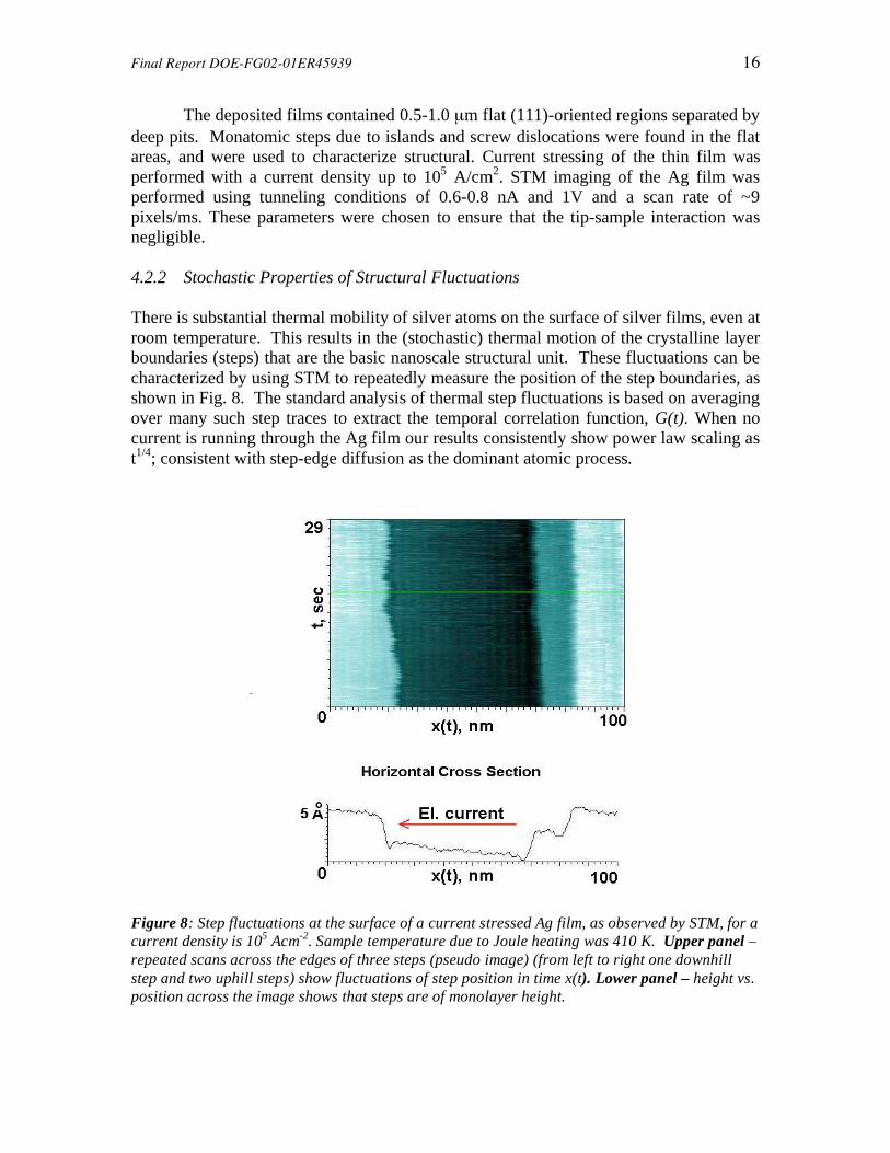
The deposited films contained 0.5-1.0 µm flat (111)-oriented regions separated by deep pits. Monatomic steps due to islands and screw dislocations were found in the flat areas, and were used to characterize structural. Current stressing of the thin film was performed with a current density up to 105 A/cm2. STM imaging of the Ag film was performed using tunneling conditions of 0.6-0.8 nA and 1V and a scan rate of ~9 pixels/ms. These parameters were chosen to ensure that the tip-sample interaction was negligible.
4.2.2 Stochastic Properties of Structural Fluctuations
There is substantial thermal mobility of silver atoms on the surface of silver films, even at room temperature. This results in the (stochastic) thermal motion of the crystalline layer boundaries (steps) that are the basic nanoscale structural unit. These fluctuations can be characterized by using STM to repeatedly measure the position of the step boundaries, as shown in Fig. 8. The standard analysis of thermal step fluctuations is based on averaging over many such step traces to extract the temporal correlation function, G(t). When no current is running through the Ag film our results consistently show power law scaling as t1/4; consistent with step-edge diffusion as the dominant atomic process.
Figure 8: Step fluctuations at the surface of a current stressed Ag film, as observed by STM, for a
current density is 105 Acm
-2. Sample temperature due to Joule heating was 410 K. Upper panel –
repeated scans across the edges of three steps (pseudo image) (from left to right one downhill
step and two uphill steps) show fluctuations of step position in time x(t). Lower panel – height vs.
position across the image shows that steps are of monolayer height.

Final Report DOE-FG02-01ER45939 17
The difficult question then becomes how to determine the effect of current stressing on the absolute behavior of step fluctuations? This problem arises because current stressing also elevates the sample temperature (via Joule heating), which has a profound influence on step fluctuations through the temperature-dependent values of the step stiffness and the time constant. To deal with this, we used the ability to heat the sample indirectly and measured step fluctuations as a function of temperature, with the results shown in Fig. 9.
Figure 9 Time correlation functions for step fluctuations on Ag films heated indirectly (no
current stressing through film).
In figure 10 we display G(t) measured experimentally by monitoring the (average) motion of the three step edges shown in fig 8 for a current of 105Acm 2 passing through a ~100nm thick silver film. For early times, G(t) exhibits the power law characteristic of thermal fluctuations ( t1/ 4). According to the predictions of the Langevin theory we have developed (see above) we expect a characteristic time for electromigration to emerge at late times. This was confirmed by fitting the measured G(t) to the form predicted. As can be seen from Fig.10, the experimentally determined G(t) for the current-stressed sample is well described by our Langevin theory with / 0 4000 . Using these parameters we estimate that, for Ag atoms diffusing along a step edge, the electromigration force is F = Z*eE , where Z* is the effective valence fit for the step up/down force directions and lies in the range between Z*= –7 and -20. To our knowledge this is the first direct determination of the magnitude of electromigration forces at surfaces.

Final Report DOE-FG02-01ER45939 18
Figure 10: Time correlation function G(t) for step fluctuations on current-stressed Ag films on
mica. The current is 105Acm
-2. Crosses: Measured G(t) when electromigration force acts in the
step up direction. Circles: Measured G(t) when electromigration force acts in the step up
direction. Solid lines are fits to the correlation function predicted by Langevin theory. During the renewal period we propose to continue this project beyond the
preliminary stage we have described here, using the experimental and theoretical tools we have developed, supported by the current award. We will conduct a temperature and current-dependent study of electromigration on stepped surfaces. Prior LKKR calculations of Z* by us show that the force at a step edge need not be symmetric with respect to the direction of the current flow . Since we can measure the magnitude of the electromigration form experimentally we will determine if the predicted asymmetry exists and find its size relative to the force itself [21]. We will also perform measurements of the spatial correlation function for fluctuations of the step edges, using Fourier transform methods to determine the wavevector dependence of G(x-x’; t), as has been done for thermal fluctuations [22, 23]. This should give us new information about the temporal evolution of the length scales in the problem and will allow us to identify the unstable wavelengths of the fluctuation instability for comparison with the predictions of our theory.
An alternative analysis of the measured data (x(t)) contains more information about the details of the stochastic “walk” of the step edge than is included in the correlation function, and may prove useful in analyzing electromigration processes and noise. We have developed a new formalism for analysis of the measured data in terms of statistical persistence, which is illustrated graphically in Fig. 11. To analyze our step fluctuations in terms of the persistence probability p( t), we divide the measured time axis into bins of width t, and then count the number of bins for which the step position does not return to the starting point of the interval. The results of the analysis, with no current stressing, are shown in Fig. 12. which exhibits the power law behavior of the persistence probability extracted from the data. A linear fit to the data yields a value for

Final Report DOE-FG02-01ER45939 19
the exponent of 0.88±0.01. This is in excellent agreement with the expected value of 7/8 for a step fluctuating via step-edge diffusion.
Figure 12: Experimentally determined persistence probability P(t) vs t for a range of
temperature for indirectly heated Ag films, calculated as described in the text (Experimental
section). The data shown were measured with �t = 0.051 s for all temperatures except T =
140oC, where �t = 0.076 s. The solid line shows the T=140
oC data vs. time (upper axis) scaled
by a factor of � ��
The data shown in Fig. 12 reveal that persistence probably A(t) for thermally
fluctuation steps in dependent only on the minimum time sampling interval. There is at present no theoretical prediction for the behavior of the persistence probability in the presence of an electromigration forcing field. However, by analogy to persistence studies in growth systems, we may expect non-trivial changes in the behavior.
Figure11: One measure of the stochastic information encompassed in a random walk x(t)
persistence probability p( t). As illustrated in the schematic graph, this is the probability of
not returning to the starting position in a specific time interval t. For the first time interval
shown, the walk is persistent (e.g. did not return to the position at to), and for the second
interval, the walk is not persistent as it returned to the starting point within the time interval
Final Report DOE-FG02-01ER45939 20
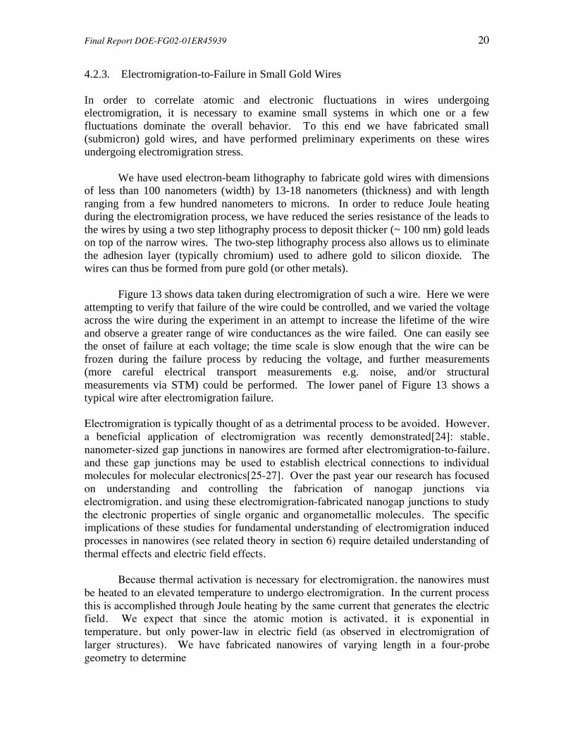
4.2.3. Electromigration-to-Failure in Small Gold Wires In order to correlate atomic and electronic fluctuations in wires undergoing electromigration, it is necessary to examine small systems in which one or a few fluctuations dominate the overall behavior. To this end we have fabricated small (submicron) gold wires, and have performed preliminary experiments on these wires undergoing electromigration stress. We have used electron-beam lithography to fabricate gold wires with dimensions of less than 100 nanometers (width) by 13-18 nanometers (thickness) and with length ranging from a few hundred nanometers to microns. In order to reduce Joule heating during the electromigration process, we have reduced the series resistance of the leads to the wires by using a two step lithography process to deposit thicker (~ 100 nm) gold leads on top of the narrow wires. The two-step lithography process also allows us to eliminate the adhesion layer (typically chromium) used to adhere gold to silicon dioxide. The wires can thus be formed from pure gold (or other metals). Figure 13 shows data taken during electromigration of such a wire. Here we were attempting to verify that failure of the wire could be controlled, and we varied the voltage across the wire during the experiment in an attempt to increase the lifetime of the wire and observe a greater range of wire conductances as the wire failed. One can easily see the onset of failure at each voltage; the time scale is slow enough that the wire can be frozen during the failure process by reducing the voltage, and further measurements (more careful electrical transport measurements e.g. noise, and/or structural measurements via STM) could be performed. The lower panel of Figure 13 shows a typical wire after electromigration failure. Electromigration is typically thought of as a detrimental process to be avoided. However, a beneficial application of electromigration was recently demonstrated[24]: stable, nanometer-sized gap junctions in nanowires are formed after electromigration-to-failure, and these gap junctions may be used to establish electrical connections to individual molecules for molecular electronics[25-27]. Over the past year our research has focused on understanding and controlling the fabrication of nanogap junctions via electromigration, and using these electromigration-fabricated nanogap junctions to study the electronic properties of single organic and organometallic molecules. The specific implications of these studies for fundamental understanding of electromigration induced processes in nanowires (see related theory in section 6) require detailed understanding of thermal effects and electric field effects.
Because thermal activation is necessary for electromigration, the nanowires must be heated to an elevated temperature to undergo electromigration. In the current process this is accomplished through Joule heating by the same current that generates the electric field. We expect that since the atomic motion is activated, it is exponential in temperature, but only power-law in electric field (as observed in electromigration of larger structures). We have fabricated nanowires of varying length in a four-probe geometry to determine

Final Report DOE-FG02-01ER45939 21
a) the temperature of the wire during electromigration (as measured by the wire
resistance) b) the scaling of the breaking voltage with temperature and electric field.
These measurements are critical for designing controlled nanogaps and for designing experiments that can rigorously tests the predictions of theory.
Figure 13. Controlled failure of a gold wire by electromigration. The upper panel shows the
conductance (left scale) of a 1 micron x 100 nm x 13 nm gold wire undergoing electromigration
stress. The applied voltage is plotted on the right axis. The voltage was reduced manually as the
wire became less conductive. The figure shows that the time scale can be made long enough and
fluctuations in conductance before failure can be made large enough that it should be possible to
“freeze” the wire in a given state for measurements of noise, and structural characterization by
e.g. scanning tunneling microscopy. The lower panel shows a scanning electron micrograph of a
similar wire after complete failure.

Final Report DOE-FG02-01ER45939 22
5. Modifying Surface Electronic Structure and Fluctuations via Adsorbate Charge Transfer
We are interested in adsorbates in the presence of electromigration fields for three reasons:
a) We may use electromigration as a method for moving adsorbates around, e.g. into gaps for molecular electronics measurements, or into patterns for controlled self assembly,
b) Transport through molecules (and across an interface from a solid conducting connector) is an exciting direction for nanoelectronics and nanosensing.
c) We may use adsorbates to modify the effects of electromigration-induced wire breaking or nanostructure evolution.
We discuss our results on each of these topics in the following. Continued work on the role of adsorbates in nanoelectronic transport will be a major effort under the renewal period.
5.1 Electron transfer through adsorbates In conjunction with Lawrence Sita (University of Maryland, also DOE supported) and Harold Baranger and Weitao Yang (Duke University), we have performed experimental studies of a novel ferrocene-containing organometallic molecule (see Fig. 22)[28]. The molecule is localized in a nanogap by first chemisorption on an unbroken nanowire, followed by breaking of the nanowire via electromigration at low temperature.
This molecule shows a low-lying resonance (< 100 meV) with differential
conductance exceeding 70% of the perfect value (G0 = 2e2/h), and exhibits the expected Lorentzian lineshape of the molecular resonance. The results are in excellent agreement with theoretical calculations by our collaborators at Duke (see Fig. 22).
This conductance magnitude is expected for resonant conduction through a
delocalized state in any molecule; that it has not been observed before is a deep mystery. Control measurements on an analogous five-ring phenylethynyl oligomer reveal orders of magnitude lower conductance similar to previous studies on conjugated all-organic molecules. Our study of the ferrocene-based species provides the first evidence for preservation of the extended electronic state in a conjugated system, as long-predicted by theoretical calculations.
This study points to a new direction in organic electronics: the incorporation of
metallocene elements in organic structures allows the realization of localized, low-lying electronic states within a conjugated organic backbone. We intend to exploit this general technique to generate more complex molecular wires containing multiple metallocene elements, in order to carefully tailor their electronic structure.

Final Report DOE-FG02-01ER45939 23
Figure 14. The novel ferrocene-containing phenyl-ethynyl dithiol is shown in (A). (B) shows the calculated constant-electron-density surface for the molecular resonance near the Fermi level. (C) shows the measured conductance of the molecule; the red curve indicates the current I, and the right curve the differential conductance G as a function of the bias voltage Vsd across the molecule. The green lines are fits to a Lorentzian lineshape. We have measured several similar junctions all exhibiting molecular resonance at Vsd < 100 mV, with G a significant fraction of Go, the quantum of conductance. (D) shows the calculated transmission of the molecule as a function of Fermi energy; a Lorentzian resonance is observed at ~50 meV above the Fermi level, in excellent agreement with experiment.

Final Report DOE-FG02-01ER45939 24
5.2 Charge transfer from adsorbates
We may use adsorbates to modify the effects of electromigration-induced wire breaking or nanostructure evolution. The dependence of surface resistivity on charge transfer from adsorbates has been demonstrated both theoretically and experimentally [29-32]. The fullerene, C60 has been found to have an especially strong effect, corresponding to a cross section for electron scattering of 50 Å2.
We begancharacterizing the electronic and structural properties of C60 adsorbed on the Ag thin films grown on mica that we have developed for electromigration studies. The extremely high mobility of C60 at room temperature [33], allows the fullerenes to diffuse and bind preferentially at step edges as shown in Fig. 15a. The C60s for well ordered arrays, with step edges that match the underlying steps of the Ag substrate as shown in Fig. 15b. At very low coverages, the C60 molecules form single chains along the step-edges, in which the different rotational orientations of the buckeyballs [34] can be observed, as shown in Fig. 16. The strong interaction of the C60 with the substrate results in two types of modifications of the substrate structure as shown in Fig. 17.
Figure 15. a) C60 islands along step edges (307nm x307nm, V=-1.58V, I=0.10nA) b) C60
monolayer on a monatomic step along [11-2] direction (16.6nm by 16.5nm, V = -1.74V, I =
0.19nA)
[1-10]

Final Report DOE-FG02-01ER45939 25
Figure 16. Individual C60 along a step edge (5.18nm x 5.18nm, V=-0.194V, I=0.504nA). Left-top
down view in color scale, right – 3D rendering of the same data. Seven different fullerene
molecules are visible with two different rotational orientations.
Figure 17. LEFT: Ripple structures near the straight edge of a C60 island (19.2nm x 20.2nm, V
= -1.5V, I = 0.10nA). Periodicity is 3.956nm-4.000nm in the [1-10] direction. RIGHT: Electron
waves along a step edge (16.19nm x 13.52nm, V=-1.744V, I=0.101nA). Periodicity is
approximately 0.5 nm. In regions where there is an area of bare substrate confined by surrounding C60 domains, the substrate takes on a periodic modulation of extremely small (0.04 nm) amplitude, with a period of about 4.0 nm. Another type of modulation, a rapidly damped periodic modulation is observed near the edges of C60 islands. The period of this structure is about 0.5 nm. Such modulations may arise due to strain effects [35, 36], but have most often been observed at cryogenic temperatures due to standing electronic waves [37, 38]. Our
[1-10]

Final Report DOE-FG02-01ER45939 26
ready observation of these modulations at room temperature indicates the very strong perturbation of the substrate electronic structure by the adsorbed fullerenes.
Figure 18. LEFT: Topography image of a monatomic step edge partly covered by C60 (105.2nm
x 105.2nm, V = -1.71V, I = 0.10nm) RIGHT: Pseudo-image obtained by scanning the STM tip
repeatedly over the middle point of the step edge (Time per line = 0.0512s, totally 2000 lines, I =
0.10nm, V = -2.22V)

Final Report DOE-FG02-01ER45939 27
6. Theory Of Current Driven Structural Fluctuations and Failure In Nanostructures In this section we report the development of the theoretical understanding of how the current carried by a nanostructure influences its structural evolution. It is well known, at the macroscopic scale, that electromigration forces, caused by current flow, lead to instabilities in structures such as metallic interconnects. As the size of current-carrying structures is reduced, surface processes, such as surface diffusion and electromigration begin to dominate the driven mass transport. For example, in bamboo lines, where the typical line width is smaller than the grain size it is well known that electromigration failure occurs within the grains and not at the grain boundaries.
We took three complementary approaches to understanding the coupling between
electrical currents and the structural evolution of nanostructures. The first is a continuum approach, based upon the Langevin formalism, where the temporal evolution of a nanostructure is modeled by following the dynamics of its surface boundary. The second is a large-scale atomistic kinetic Monte Carlo simulation that contains an explicit model of the atomic motion that constitutes the driven bulk and surface diffusion occurring in/on a nano-scale interconnect. Thirdly, we have used Langevin theory to study fluctuations in the fundamental nanoscale “unit”; a monolayer step and was described in section 1.4.
6.1. Langevin Analysis
Essential ingredients of this model are the capillary forces, the electromigration
force and the curvature driven surface diffusion. This leads to a fourth-order non-linear partial differential equation that governs the evolution of the bounding surface.
Prior research has employed linear stability analysis to study the dynamics of
existing voids in interconnects under electromigration. This work predicts the emergence of a transgranular slit from the void, a feature that is commonly observed in accelerated failure experiments on interconnects. However, to our knowledge, it is not understood how and why the void forms in the first place. Indeed, stability analysis leads to the conclusion that a defect-free interconnect is linearly stable under electromigration conditions. Recently we have shown that a more careful analysis, using multiscale methods, leads to the conclusion that void formation can be initiated by a critical fluctuation of the surface profile. The fluctuation initially decays, similar to the predictions of the linear analysis, but then grows after an incubation period has expired. Some typical results are shown in Fig. 23.
We find that the void develops into a wedge-like structure similar to that observed
experimentally. Numerical simulations show that, the void size grows as (t tinc )1/ 4where
tinc is the incubation time. This slow growth rate appears to obey a universal scaling relation that we hope to understand by further analysis of the problem as detailed in the

Final Report DOE-FG02-01ER45939 28
renewal proposal. Eventually we hope to use this model to obtain a quantitative estimate of the time to failure of an interconnect. We will do this by analyzing:
• The temporal statistics of the thermally driven critical fluctuation that we
believe to be a so-called first-passage process. • The incubation time and how it depends on the amplitude and wavelength
of the critical fluctuation. • The time-taken for the void to grow to the critical size that initiates the
emergence of the transgranular slit (that ultimately breaks the line).
Figure 19. The temporal evolution of the amplitude of a sinusoidal fluctuation (wavelength ) at the surface of an Al interconnect, as predicted by the Langevin model. Fluctutations with an initial amplitude smaller than 0.14 decay exponentially with a time constant proportional to
t 1/ 4 . Fluctuations with amplitude larger than this critical amplitude decay initially but then grow to form a wedge-like void with a time constant propotional to t +1/ 4 .
6.2. Kinetic Monte-Carlo Simulation Of Electromigration Failure At The
Nanoscale: Fluctuations and Reliability We have developed and implemented a large-scale kinetic Monte Carlo simulation that allowed us to study the temporal evolution of nanostructures under current stressing. This simulation uses standard KMC methods for a fully three-dimensional structure and is designed to bridge the atomic and mesoscopic length scales. All possible bulk and surface diffusional events are modeled in a way that explicitly satisfies the condition for microscopic reversibility. For our initial study of Al nanostructures, the atomic hopping

Final Report DOE-FG02-01ER45939 29
rates were derived from an inter-atomic potential fit to first principles molecular dynamics simulations, LDA and EAM calculations. A key aspect of this simulation is the incorporation of biased diffusion driven by a current. The detailed electromigration forces are determined from our previous LKKR calculations. In order to understand electromigration, even in accelerated current-stressing experiment, the simulation needs to follow the evolution of structures on length scales of a micron and for time-scales exceeding seconds. This requires a highly efficient computational model and correspondingly powerful computational resources. Our approach has been to develop a parallel simulation based on MPI that runs across a Beowulf cluster. To do this, during summer of 2001 a 32 node Beowulf cluster was designed and then installed in the Physics Department at UMBC. This computational resource was funded by the State of Maryland and is currently used exclusively for this project. At present, the cluster is used to model simultaneously the failure of Al interconnects between the nano and micron scale.
The simulation we have developed allowed us to examine both microscopic
fluctuations and failure mechanisms in nanostructure with, and without, electromigration present. It is well known that cylindrical bodies are unstable with respect to surface diffusion at temperatures well below the melting point; a manifestation of the Raleigh instability driven by thermal fluctuations. Very recently, the first SEM observation of this thermal instability in nanowires was made. This experimental study observed the break up of copper nanowires (r=15-20nm) into nanospheres (see Fig. 24).
Figure 20. The thermal Rayleigh instability in nanowires. Left panel: SEM images of 30-
40nm diameter copper nanowires after annealing in vacuum for 30 minutes at 400oC (top), 500
oC
(middle) and 600oC (bottom). The melting point of copper is 1085
oC. From reference [39, 40].
Right panel: Atomistic KMC simulation of the annealing of a 15nm diameter Al nanowire at
400oC showing a similar pattern of morphological evolution. The melting point of Al is 660
oC
For comparison, figure 16 shows the results of our KMC simulation of the
thermal failure of 10nm diameter Al nanowire during annealing at 400C. Snapshots of the simulation are shown when the wire breaks (t=1ms, top panel) and for t=2ms and 10ms and reproduce qualitatively the features seen in the SEM study of copper nanowires (Fig. 24). Although the time scale of the evolution of the Rayleigh instability is much

Final Report DOE-FG02-01ER45939 30
shorter for our simulation, this can be attributed to the lower melting temperature of Al (660C) and the smaller diameter of the wires in our simulation.
Using our atomistic KMC simulation we have been able to study the failure dynamics (scaling) and failure statistics of Al nanowires, information that will ultimately allow us to predict time to failure on the nanoscale. Figure 25 shows the mininum radius, rmin (t), of a collection of 34 identical nanowires, plotted as a function of time. The decrease in rmin (t) signals the onset of the Rayleigh instability and the nanowire open circuits when rmin (t = t f ) = 0; t f is the time to failure.
Figure 21. The temporal evolution of the minimum line radius of an ensemble of 34
initially rectangular, 15nm wide, Al nanowires with (100) faces exposed. T=400C. Collapse of
the minimum line width to zero is the signature of failure of the line (open circuit). The average
failure time is 1.1ms.
Careful analyis of simulations performed at different temperatures indicates that the minimum radius of nanowires scales as a power law in time: rmin (t) (t f t)1/ 4 (see
Fig. 26). This result was confirmed by a continuum theory. Preliminary results indicated that t f (T) is of Arrenhius form that suggests there is indeed a rate-limiting diffusion
event, or events, for thermal failure. We also tried to understand how electromigration affects the failure mode and
time to failure of nanowires. We have accumulated consistent evidence (such as that shown in Fig. 27) that the effect of electromigration at the nanoscale is to increase the time to failure beyond that expected for the Rayleigh instability driven by thermal fluctuations alone. Thus it appears possible that, at the nanoscale, electromigration tends to suppress the Rayleigh instability. This counter-intuitive behavior is a completely new feature of our simulations and is completely opposite to the behavior seen at the macroscopic scale. This initial result serves to emphasize the importance of atomistic, microscopic models in capturing the physics of the reliability of nanostructures.

Final Report DOE-FG02-01ER45939 31
Figure 22. A plot of the rmin (t f t) showing how the breaking of a typical nanowire scales as a
power law: rmin (t) (t f t)1/ 4 .
Figure 23. A histogram showing the time to failure of an ensemble of 32 initially rectangular,
15nm Al nanowires with (100) faces exposed. Each interconnect carries an initial current of 1µA
at T=600C.
At present we have no understanding of why electromigration suppresses the Rayleigh instability. There is, in the literature, theoretical evidence that this effect can be caused by the quantization of the electronic states in the nanowire so that the kinetic energy of the conduction electrons becomes a significant contribution towards the total “shape” energy of the wire. However, since such effects are not included in our model, the suppression

Final Report DOE-FG02-01ER45939 32
we observe must be attributed to some structural feature. Preliminary studies have shown that a key difference between thermal and electromigration induced instabilities is that, in the former case, the nanowire breaks into segments of equal volume while, in the latter case, the individual segments have significantly different volumes and are not uniformly spaced apart. The length-scale for the uniform break-up by thermal failure is the wavelength of the most unstable mode, a quantity that depends on only one parameter: the initial radius of the nanowire. It seems likely that the phenomenon we have observed in our simulations of current stressing reflects the existence of more than one maximally unstable mode. This would explain the emergence of a number of distinct length scales as a nanowire fails under electromigration conditions. To explain such an effect we must go beyond linear theory and one approach will be to use perturbation theory to investigate the growth and coupling of the basic modes. We believe that what we have observed in our simulations may be mapped onto the Turing [41, 42] model of spatial pattern formation. It has been noted the thermal break up of nanowires may have applications in nano-patterning, where the individual elements of the pattern are the segments between the breaks in the wire [39, 40]. In this case the volume and spacing of the each segment of the Nan pattern is determined only by the initial conditions of the nanowire, although it is possible to change the resulting cylinder like structures to spheres by increasing the annealing time. From the point of view of Nan patterning, such an approach is not optimal, simply because it is not possible, by thermal processing alone, to vary the size of, or spacing between, the individual nanostructures that make up the pattern. The emergence of more than one maximally unstable mode under electromigration conditions suggests that the current flowing through the nanowire might be used as a new parameter to alter the pattern created as the wire breaks up.

Final Report DOE-FG02-01ER45939 33
7. Nanowires for fundamental electromigration studies and sensing
7.1. Uniform and Reproducible Nanogap Fabrication
The general technique of electromigration-to-failure for nanogap formation was pioneered by Hongkun Park[24] (with Paul McEuen at Berkeley, and independently at Harvard). Park’s technique involved a nanoscale overlap of two electrodes formed by shadow evaporation at two angles. This process produces a junction structure which is highly irreproducible: small differences in resist bridge height and thickness, and the uncontrolled boundary between the two metal electrodes, result in a junction nanostructure which is difficult to control.
Our technique for nanogap junction formation starts with uniform narrow metal
wires (nanowires) defined by electron-beam lithography (EBL). Subsequent lithography steps are used to contact the nanowire with larger electrodes. In initial experiments, the nanowires were fabricated in-house and later using the EBL facilities at the Cornell Nanoscale Facility (CNF) to fabricate arrays of nanowires on the wafer scale (see Fig.24). The Cornell EBL facilities are able to produce ~30 nm lithography with excellent uniformity. We were able to fabricate ~100 arrays of 20 wires each at CNF, and can now easily repeat this result in one week’s work at CNF. Tests on electromigration-to-failure of the CNF nanowires show that the voltage required to break the wires is lower, and more narrowly distributed, than the wires produced at Maryland (see Fig. 25).
Studies of wires fabricated at Maryland indicated that at low temperature (~4 K) nanogaps of order 1 nm could be formed, as revealed by a finite tunneling current across the gap after breaking. Upon warming these junctions to room temperature, the gap size increased, and was observed by SEM to be typically several nanometers. Interestingly, studies of the CNF nanowires show that the tunnel conductance of nanogaps formed at low temperature is considerable, sometimes a significant fraction of Go, the conductance quantum, the conductance value expected for a single atomic bridge. If the substrate temperature is higher during breaking, the residual conductance of the nanogap is reduced, and at room temperature we find we can produce stable nanogaps with a low but finite tunnel conductance, indicating a gap size on the order one nanometer (see Fig. 26). This important result paves the way for use of electromigration-fabricated nanogaps in applications such as sensing at room temperature. This opens many new avenues for study, including binding of molecules at room temperature in already-formed nanogaps (previously molecules where physisorbed or chemisorbed on wires before breaking), and electrochemical studies of molecules in nanogaps in solution. This result is being prepared for publication[45].

Final Report DOE-FG02-01ER45939 34
Figure 24. Gold nanowire array fabricated at the Cornell Nanoscale Facility. The top row shows two optical micrographs (left and middle) and a scanning electron micrograph (right) of the device. There are 20 nanowires, plus an aluminum gate strip which run underneath all the wires. A scanning electron micrograph of a broken wire is shown in the lower right; the small break is difficult to image even with the SEM. A schematic of the nanogap junction and gate is at lower left.
0.0 0.5 1.0 1.5 2.00
5
10
15
20
Num
ber
of
wires
Breaking Voltage (V)
B1 B2
0.0 0.5 1.0 1.5 2.00
5
10
15
20
Num
ber
of
Wires
Breaking Voltage (V)
EM16 EM17
Figure 25. Histograms of breaking voltages for 40 nanowires fabricated at Maryland (upper graph) and 40 nanowires fabricated at the Cornell Nanoscale Facility (CNF, lower graph). The nanowires fabricated at CNF break at lower voltage, and the breaking voltage is more reproducible.

Final Report DOE-FG02-01ER45939 35
0 50 100 150 200 250 3001
10
100
1000
10000
100000
G (
nS
)
Tbreak
(K)
Figure 26. Residual conductance of nanogaps as a function of the substrate temperature during wire breaking. Nanowires which are broken at low temperatures show significant residual conductance, indicating nearly closed gaps. Wires broken at higher temperature 7.2.1 Solid State Ionic Transport Recent reports of the growth of small Ag wires between sharp electrodes [46] led us to consider the possibility of developing an in situ growth method for creating ultra-clean, well defined wires with automatic contacts to pre-positioned electrodes. The growth process involves the superionic silver halides, and capitalizes on our investment in developing single crystal silver films on insulating mica substrates.
Superionic conductors are compounds that exhibit exceptionally high values of ionic conductivity in the solid state. Ag+ and Cu+ halide are the most widely studied superionic conductors. In the case of AgI, the material generally exists under ambient conditions as a two phase mixture of the hexagonal wurtzite and cubic zincblende structures. Heating AgI causes a first-order structural phase transition to the superionic phase at 420 K, in which the ionic conductivity increases by around three orders of magnitude, remaining essentially constant up to the melting point of 825 K. The anion sublattice forms a bcc array, the two Ag+ per unit cell predominantly occupy the 12 tetrahedral sites per unit cell and undergo rapid jump diffusion between them. This occurs in <110> directions via the trigonal interstices rather than in <100> directions via the octahedral ones. This is a typical type-I superionic transition.
In the present study, we use the superionic AgI phase as a substrate from which to grow silver nano-wires with a STM tip. Setting a negative bias on the STM tip we can

Final Report DOE-FG02-01ER45939 36
grow and neutralize silver nano-wires with the tunnel current while retracting the tip. Such wires can have a radius from 10nm to sub-micron size and thus are exactly the appropriate size to serve as a platform for studies of electromigration phenomena and current crowdings. a) b)
c)
Figure 27: UHV SEM images of STM tip interacting with AgI/Ag film. a) tip approach under
positive tip bias, b) immediate onset of wire growth upon reversal of tip polarity, c) growth of
Ag nanowires as tip is retracted under negative tip bias. In our preliminary study of the fabrication of these wires in UHV, silver films 200~400nm thick were deposited on a mica substrate using e-beam deposition. The substrate was then exposed to iodide vapor at 180 ºC in air for a few seconds to create a thin layer of AgI on the surface of the silver film. The sample was transferred to our ultra-high vacuum SEM-SPM system and heated in situ to above 420 K to obtain the superionic phase. An approach by the STM tip was performed with a positive bias on the tip, as shown in Fig. 27a. Silver nano-wires grow as soon as the bias is flipped to the negative side as shown in Fig. 27b. With the help of the SEM it is possible to retract the tip and pull out long nano-wires from the substrate with the results shown in Fig. 27c.

Final Report DOE-FG02-01ER45939 37
Preliminary results are highly promising. High resolution imaging of the wire network reveals single wires of 100 nm width. We are developing pre-patterned electrode configurations that will allow the growth of better-controlled wire networks with principle orientation parallel to the surface. The growth process leaves the wires connected automatically to the base electrode.
7.2.2 Growth of wires in mesorporous membranes In situ solid state electrochemical growth has the exciting potential to provide extremely clean, well controlled nanoscale wires. However, this approach is limited in materials diversity as it can only be used successfully with the relatively small class of materials that form superionic conductors. To overcome this materials limitation, we are investigating in parallel the use of mesoporous alumina membranes as templates for the growth of single crystal nanowires [47]. The template membranes typically are 40 µm thick and contain a pseudo-hexagonal array of pores with diameters that can be controlled on the scale of 10-200 nm easily. Materials can be plated into the pores electrochemically, and then the supporting alumina can be etched away leaving a free-standing bundle of nanowires.
Recently, there have been many reports that the crystallinity of the nanowires can be controlled using pulsed deposition techniques [48, 49]. We have carried out preliminary fabrication using this approach, with promising results. We plan to use this technique for the fabrication of a wide variety of nanowires. These will initially be transferred to substrates via spin-coating or ultra-sonication and contacted onto pre-formed (or subsequent find and contact) electrodes for simultaneous structure/transport measurements. These investigations will be correlated not only with electromigration studies, but also with sensor development, as outlined in another section of this report.

Final Report DOE-FG02-01ER45939 38
8. References
1. Thompson, C.V. and J.R. Lloyd, Electromigration and IC interconnects. MRS Bulletin, 1993. 18(12): p. 19-25.
2. Sorbello, R.S., Theory of Electromigration, in Solid State Physics, H. Ehrenreich and F. Spaepen, Editors. 1997, Academic Press, New York,. p. 159-231.
3. Ho, P.S. and A.T. Kwok, Electromigration in metals. Reports on Progress in Physics, 1989. 52: p. 301.
4. Kuhn, P. and J. Krug. Islands in the Stream: Electromigration-Driven Shape Evolution with Crystal Anisotropy. in Proceedings of the Oberwolfach workshop on Multiscale Modeling in Epitaxial Growth. 2004.
5. Arzt, E., et al., Electromigration failure by shape change of voids in bamboo lines. Journal of Applied Physics, 1994. 76: p. 1563-1571.
6. Verbruggen, A.H., Fundamental questions in the theory of electromigration. IBM J. Res. Develop., 1988. 32: p. 93-98.
7. Schimschak, M. and J. Krug, Surface Electromigration as a Moving Boundary Value Problem. Physical Review Letters, 1997. 78: p. 278-281.
8. Mahadevan, M. and R.M. Bradley, Stability of a circular void in a passivated, currentcarrying metal. Journal of Applied Physics. 79: p. 6840-6847.
9. Gungor, M.R. and D. Maroudas, Theoretical analysis of electromigration-induced failure of metallic thin lms due to transgranular void propagation. Journal of Applied Physics, 1999. 85: p. 2233-2246.
10. Wang, W., Z. Suo, and T.-H.Hao, A simulation of electromigration-induced transgranular slits. Journal of Applied Physics, 1996. 79: p. 2394-2403.
11. Schimschak, M. and J. Krug, Electromigration-driven shape evolution of two-dimensional voids. Journal of Applied Physics, 2000. 87: p. 695-703.
12. Kim, J.H., et al., A phase field model for electromigrationinduced surface evolution. Metals and Materials International, 2003. 9: p. 279-286.
13. Gungor, M.R. and D. Maroudas, Current-induced non-linear dynamics of voids in metallic thin lms:morphological transition and surface wave propagation. Surface Science, 2000. 461: p. L550-556.
14. Suo, Z., W. Wang, and M. Yang, Electromigration instabilities:transgranular slits in interconnects. Applied Physics Letters, 1994. 64: p. 1944-1946.
15. Mahadevan, M., R.M. Bradley, and Phys. Rev. B 59 (1999), Simulations and theory of electromigration-induced slit formation in unpassivated single-crystal metal lines. Physical Review, 1999. B59: p. 11037-11046.
16. Yongsunthon, R., et al., Mapping Electron Flow Using Magnetic Force Microscopy. Applied Physics Letters, 2003. 82: p. 3287-9.
17. Rous, P.J., et al., Real Space Imaging of Current Distributions at the Sub-Micron Level Using Magnetic Force Microscopy: Inversion Methodology. Journal of Applied Physics, 2004. 95(5): p. 2477-86.
18. Yongsunthon, R., et al., Test of response linearity for magnetic force microscopy data. 92, 2002. 92(3): p. 1256-61.
19. Yongsunthon, R., et al., Phase Imaging of Buried Structures. Applications of Surface Science, 2003. 210: p. 6-11.

Final Report DOE-FG02-01ER45939 39
20. Yongsunthon, R., et al., Defect Signatures In MFM Current Imaging. Journal of Applied Physics, 2004: p. (in preparation).
21. Blank, LKKR Of Force Asymmetry. 22. Bartelt, N.C., et al., Surface Science, 1992. 273: p. 252. 23. Bartelt, N.C., T.L. Einstein, and E.D. Williams, Surface Science, 1994. 312: p.
411. 24. Park, H., et al., Fabrication of metallic electrodes with nanometer separation by
electromigration. Applied Physics Letters, 1999. 75(2): p. 301-303. 25. Park, H., et al., Nano-mechanical Oscillations in a Single-C60 Transistor. Nature,
2000. 407: p. 57. 26. Park, J., et al., Coulomb blockade and the Kondo effect in single-atom transistors.
Nature, 2002. 417(6890): p. 722-725. 27. Liang, W., et al., Kondo resonance in a single-molecule transistor. Nature, 2002.
417(6890): p. 725-729. 28. Getty, S.A., et al., Designing a high conductance molecular wire. submitted to
Physical Review Letters. 29. Persson, B.N.J., Surface resistivity and vibrational damping in adsorbed layers.
Physical Review, 1991. B 44: p. 3277-3296. 30. Persson, B.N.J. and A.I. Volokitin, Comment on "Brownian motion of
microscopic solids under the action of fluctuating eletromagnetic fields". Physical Reviw Letters, 1999. 84: p. 3504.
31. Hebard, A.F., R.R. Ruel, and C.B. Eom, Charge transfer and surface scattering at C-60 planar interfaces. Physical Review, 1996. B54: p. 10452-14060.
32. Hebard, A.F., et al., Charge transfer at aluminum-C60 interfaces in thin-film multilayers. Physcial Review, 1994. B50(17740-17743).
33. Altmah, E.I. and R.J. Colton, The interaction of C60 with noble metal surfaces. Surface Science, 1993. 295: p. 13-33.
34. Grobis, M., X. Lu, and M.F. Crommie, Local electronic properties of a molecular monolayer: C60 on Ag(001). Physical Review, 2002. B 66: p. 161408.
35. K.H.Ahn and A.R. Bishop, Atomic scale lattice distortions and domain wall profiles. Physical Review, 2003. B68: p. 092101.
36. Wang, L. and H. Cheng, Density functional study of the adsorption of a C60 monoayer on Ag(111) and Au(111) surfaces. Physical Review, 2004. B69.
37. Crommie, M.F., C.P. Lutz, and D.M. Eigler, Imaging standing waves in a two-dimensional electron gas. Nature, 1993. 363: p. 524-527.
38. Pivetta, M., et al., Reading the ripples of confined surface-state electrons: Profiles of constant integrated local density of states. Physical Review, 2003. B67: p. 193402.
39. M.E. Toimil Molares, et al., Applied Physics Letters, 2003. 82: p. 2139. 40. M.E. Toimil Molares, et al., Nanotechnology, 2004. 15: p. 201. 41. Murray, J.D., Mathematical Biology. Biomathematics Texts. 1989: Springer-
Verlag. 42. Turing, A.M., The Chemical Basis For Morphogenesis. Phil. Trans. Roy. Soc.
Lond., 1952. B237: p. 37-72. 43. Ralls, K.S., D.C. Ralph, and R.A. Buhrman, Individual-defect electromigration in
metal nanobridges. Physical Review, 1989. B40(11561-70).

Final Report DOE-FG02-01ER45939 40
44. Holweg, P.A.M., et al., Ballistic electron transport and two-level resistance fluctuations in noble-metal nanobridges. Physical Review, 1991. B45: p. 9311.
45. Esen, G., S.A. Getty, and M.S. Fuhrer, Room temperature stable molecular scale nanogap electrodes. in preparation.
46. Terabe, K., et al., Formation and disappearance of a nanoscale silver cluster realized by solid electrochemical reaction. Journal of Applied Physics, 2002. 91: p. 10110-10114.
47. Yamada, K., R. Gaparac, and C.R. Martin, Electrochemical and Transport Properties of Templated Gold/Polypyrrole-Composite Microtubule Membranes. Journal of the Electrochemical Society, 2004. 151: p. E14-19.
48. Sauer, G., et al., Highly ordered monocrystalline silver nanowire arrays. Journal of Applied Physics, 2002. 91: p. 3243-3247.
49. Pang, Y.T., et al., Copper nanowire arrays for infrared polarizer. Applied Physics A, 2003. 76: p. 533-6.
50. Walter, E.C., F. Favier, and R.M. Penner, Palladium Mesowire Arrays for Fast Hydrogen Sensors and Hydrogen-Actuated Switches. Analytical Chemistry, 2002. 74: p. 1546-1553.
51. Kaltenpoth, G., et al., Multimode Detection of Hydrogen Gas Using Palladium-Covered Silicon micro-Channels. Analytical Chemistry, 2003. 75: p. 4756-4765.
52. Watson, J., The tin oxide gas sensor and its applications. Sensors and Actuators B: Chemical, 1984. 5: p. 29-42.
53. Schierbaum, K.D., U. Weimar, and W. Gopel, Comparison of ceramic, thick-film and thin-film chemical sensors based upon SnO2. Sensors and Actuators B: Chemical, 1992. 7(1-3): p. 709-716.
54. Shukla, S., et al., Synthesis and characterization of sol-gel derived nanocrystalline tin oxide thin film as hydrogen sensor. Sensors and Actuators B: Chemical, 2003. 96(1-2): p. 343-353.
55. Gong, J., et al. Nanocrystalline mesoporous SMO thin films prepared by sol gel process for MEMS-based hydrogen sensor. in MOEMS and Miniaturized Systems IV. 2004. San Jose, CA, USA: SPIE.
Final Report DOE-FG02-01ER45939 41
9. Publications 1. R. Yongsunthon, P.J. Rous, A. Stanishevsky, K. Siegrist and E.D. Williams,
Phase Imaging of Buried Structures. Applications of Surface Science, 2003. 82: p. 3287-9.
2. R. Yongsunthon, E.D. Williams, A. Stanishevsky and P. Rous, Magnetic Force Microscopy Imaging of Current Paths. Materials Research Society Symposium Proceedings, 2003. 738: p. G5.6.1-6.
3. R. Yongsunthon, E.D. Williams, A. Stanishevsky and P.J. Rous, Mapping Electron Flow Using Magnetic Force Microscopy. Applied Physics Letters, 2003. 82: p. 3287-3289.
4. P.J. Rous, R. Yongsunthon, A. Stanishevsky and E.D. Williams, Real-Space Imaging of Current Distributions at the Sub-Micron Scale Using Magnetic Force Microscopy: Inversion Methodology. Journal of Applied Physics, 2004. 95: p. 2477-2486.
5. E.D. Williams, Nanoscale Structures: Lability, Length Scales, and Fluctuations. Materials Research Society Bulletin, 2004. September: p. 621-629.
6. O. Bondarchuk, D.B. Dougherty, M. Degawa, M. Constantin, C. Dasgupta and S. Das Sarma, Correlation Time for Step Structural Fluctuations. Physical Review B, 2004. 71: p. 045426.
7. D.B. Dougherty, C. Tao, O. Bondarchuk, W.C. Cullen, M. Constantin, C. Dasgupta and S. Das Sarma, Sampling Time Effects for Persistence and Survival in Step Structural Fluctuations. Physical Review E, 2005. 71: p. 021602(8).
8. M. Degawa, F. Szalma and E.D. Williams, Nanoscale Equilibrium Crystal Shapes. Surface Science, 2005. 583: p. 126-138.
9. M. Degawa and E.D. Williams, Constrained evolution of nano-crystallites. Physical Review B, 2006: p. in press.
10. M. Degawa, W. Cullen, A. Pimpinelli, T.L. Einstein and E.D. Williams, Distinctive fluctuations in a confined geometry. Physical Review Letters, 2006: p. in press.
11. O. Bondarchuk, E.D. Williams, T. Bole and P.J. Rous, Biased Fluctuations under Electromigration Force. 2006: in preparation.
12. P.J. Rous, E.D. Williams and T. Bole and, Step Edge Fluctuations under Electromigration Conditions. 2006: submitted to Physical Review B.
13. G. Esen, S.A. Getty, and M. S. Fuhrer, Formation of Molecular-Scale Gold Nanogap Junctions via Controlled Electromigration, in Electronic Properties of Novel Nanostructures, pp. 534-537, H. Kuzmany, J. Fink, M. Mehring, and S. Roth, Editors (AIP Conference Proceedings, New York, 2005). 14. Temperature and Current Stressing Effects on Step Fluctuations on Ag Thin
Films, in preparation 2006 (A. Bondarchuk, M. Degawa, P.J. Rous and E.D. Williams)
16. Defect Signatures in MFM Current Imaging, in preparation 2006 (R. Yongsunthon, A. Stanishevsky, P.J. Rous and E.D. Williams).

Final Report DOE-FG02-01ER45939 42
17. Theory and Modelling of Failure Dynamics and Reliability of Nanoscale Al
Interconnects in preparation 2006 (P.J. Rous and T. Bole). 18. Designing a high conductance molecular wire, Stephanie A. Getty, Chaiwat
Engtrakul, Lixin Wang, Rui Liu, San-Huang Ke, Harold U. Baranger, Weitao Yang, Michael. S. Fuhrer, and Lawrence R. Sita, submitted to Physical Review Letters.
19. Temperature Control of Electromigration to form Gold Nanogap Junctions, G. Esen and M.S. Fuhrer, Applied Physics Letters 87 263101 (2005).
10. Presentations
1. Structural Fluctuations, Electrical Response and Relibability of Nanostructures, DOE 20th Symposium on Energy Engineering Sciences, Argonne National Laboratory, May 2001.
2 Fluctuations of Nanoscale Structures: Integrated Nanosystems 2002, Berkeley, California, September 2002.
3. Nanoscale Fluctuations on Solid Surfaces: Dutch Condensed Matter Physics Conference, Veldhoven, The Netherlands, December 2002 (Plenary talk).
4. Surface Lability: How, why and when surfaces reorganize to form self-patterned substrates, Gordon Research Conference on Condensed Matter Physics, June 2003
5. Fluctuations and Instabilities in Nanoscale Materials, Turnbull Award Lecture, Materials Research Society, Boston, December 2003.
6. Fluctuations on Nanoscale Structures: Correlation Length, Persistence and Survival, Lorentz Workshop on Collective Aspects of Stochastic Non-Equilibrium Phenomena at Surfaces and Interfaces, Lorentz Center, Leiden University, June 2004
7. Length Scales and Time Scales in First-Passage Behavior of Step Wandering on Solid Surfaces, 22nd International Conference on Statistical Physics, Bangalore, India, July 2004 (invited)
8. One-dimensional interfaces in Two-dimensional Materials Structures, Materials Research Society, Boston, November 2004 (invited)
9. One-dimensional interfaces in Two-dimensional Materials Structures, Workshop on Nanoscale Material Interfaces: Experiment, Theory and Simulation, Institute for Mathematical Sciences, U. of Singapore, January 2005 (invited)
10. The effect of boundary conditions on evolution of nanocrystallite structure: application to Pb crystallite relaxation, M. Degawa, D.B. Dougherty, K. Thürmer and E.D. Williams, American Physical Society 2004. 11. Modeling Nano-Structure Evolution in the Continuum Step Model: Decay of Pb crystallites, M. Degawa, D.B. Dougherty, K. Thürmer and E.D. Williams, T. Stasevich and T.L. Einstein, American Vacuum Society, 2003.

Final Report DOE-FG02-01ER45939 43
12. Magnetic Force Microscopy Observation of Spatial Variation in Current Density, R. Yongsunthon, Contributed Talk, Materials Research Society Meeting, November 2002, Materials Research Society Fall 2002 Graduate Student Gold Award for Excellence in Research 13. Magnetic Force Microscopy Observation of Spatial Variation in Current Density, R. Yongsunthon, Contributed Talk, Non-contact Atomic Force Microscopy Conference 2002, Canada, August 2002 14. Magnetic Force Microscopy Observation of Current Crowding, R. Yongsunthon, Contributed Talk, Materials Research Society Meeting, November 2004