strong topological metal material with multiple dirac cones...physical review b 93, 045315 (2016)...
TRANSCRIPT

PHYSICAL REVIEW B 93, 045315 (2016)
Strong topological metal material with multiple Dirac cones
Huiwen Ji,1 I. Pletikosic,2,3 Q. D. Gibson,1 Girija Sahasrabudhe,1 T. Valla,3 and R. J. Cava1
1Department of Chemistry, Princeton University, Princeton, New Jersey 08544, USA2Department of Physics, Princeton University, Princeton, New Jersey 08544, USA
3Condensed Matter Physics and Materials Science Department, Brookhaven National Laboratory, Upton, New York 11973, USA(Received 1 December 2015; published 25 January 2016)
We report a new, cleavable, strong topological metal, Zr2Te2P, which has the same tetradymite-type crystalstructure as the topological insulator Bi2Te2Se. Instead of being a semiconductor, however, Zr2Te2P is metallicwith a pseudogap between 0.2 and 0.7 eV above the Fermi energy (EF ). Inside this pseudogap, two Diracdispersions are predicted: one is a surface-originated Dirac cone protected by time-reversal symmetry (TRS),while the other is a bulk-originated and slightly gapped Dirac cone with a largely linear dispersion over a2 eV energy range. A third surface TRS-protected Dirac cone is predicted, and observed using angle-resolvedphotoemission spectroscopy, making Zr2Te2P the first system, to our knowledge, to realize TRS-protected Diraccones at M points. The high anisotropy of this Dirac cone is similar to the one in the hypothetical Dirac semimetalBiO2. We propose that if EF can be tuned into the pseudogap where the Dirac dispersions exist, it may be possibleto observe ultrahigh carrier mobility and large magnetoresistance in this material.
DOI: 10.1103/PhysRevB.93.045315
I. INTRODUCTION
Three-dimensional (3D) Dirac materials that host masslessDirac fermions have recently received widespread attentiondue to their exotic properties such as extremely high carriermobility and large magnetoresistance [1–3]. They are the3D analogs of graphene, with Dirac points and “photonlike”dispersions in their electronic structures. The Dirac bands canhave different origins. Breaking their protecting symmetriescauses the Dirac point to be gapped and leads to a Diracband where the electrons have mass. Topological insulatorssuch as Bi2Te3 and Bi2Se3 have a finite bulk band gapdue to spin-orbit coupling (SOC) and chiral, massless Diracsurface states [4,5]. In these materials, the degeneracy at thesurface Dirac point is protected by time-reversal symmetry(TRS) [6,7]. The Dirac points are doubly degenerate andthe corresponding surface states are strongly spin polarized.By contrast, another group of 3D Dirac materials—Diracsemimetals—have Dirac dispersions in the bulk electronicstructure with Dirac points that are protected by crystallinesymmetries [8]. Their Dirac points are fourfold degenerateand do not have spin polarization. Recently established Diracsemimetals include Cd3As2 [2,9,10] and Na3Bi [3,11].
Given the potential applications and intrinsically unusualphysics of 3D Dirac materials, new candidates are wanted todiversify the current family. Among different material systems,layered chalcogenides containing heavy elements are favoredfor having the band degeneracies necessary for either 3D Diracdispersions or topologically protected surface states. Theirlayered structures and easy cleavage allow visualization of anyDirac dispersion that may be present through angle-resolvedphotoemission spectroscopy (ARPES) study. The tetradymitestructure type is of particular importance as it hosts many3D topological insulators, namely, Bi2Te3, Bi2Se3, Sb2Te3,Bi2Te2Se, and Bi2Te1.6S1.4 [5,12,13]. These materials all havea single 2D surface Dirac cone in the Brillouin zone. Here,we report an additional strong topological metal, Zr2Te2P, inthe tetradymite structure family. Its multiple Dirac features,which originate from both the bulk and the surface, are
theoretically predicted and experimentally observed usingARPES. In contrast with the majority of currently knowntopological materials, which are based on s-p band inversions,the band inversions in Zr2Te2P are of the d-p type.
II. EXPERIMENT
In this work, single crystals of both pristine Zr2Te2P andslightly Cu-intercalated Cu0.06Zr2Te2P were grown throughvapor transport [14]. Initially, adding copper was intendedto increase the EF of pristine Zr2Te2P because copperintercalation in layered chalcogenides has been known toinject electrons while maintaining the overall band structure[15,16]. We could intercalate only 0.06 Cu per formula unit,(determined using single-crystal x-ray diffraction; see TableI in the Supplemental Material [17]), i.e., 0.03 electronsper Zr, which can raise EF only minimally in this metallicmaterial. We found, however, that the as-grown Cu intercalatedcrystals have higher quality, and therefore the experimentalcharacterizations were performed on Cu0.06Zr2Te2P, whichwe designate as Cu-Zr2Te2P in the following.
The sample synthesis followed the methods reportedelsewhere [14]. Polycrystalline samples of Zr2Te2P andCu-Zr2Te2P were made through traditional solid state syn-thesis at 1000◦C. The starting formulas were Zr2Te2P andCu0.8Zr2Te2P, respectively. Careful control of the temperatureand close monitoring were required to avoid explosion dueto phosphorus’s high vapor pressure and the large enthalpyof formation of the product. The polycrystalline powder wasthen loaded into a quartz ampoule containing iodine as atransport agent. A temperature gradient for chemical vaportransport was created by using a horizontal two-zone furnacewith the source end set at 800 °C and the sink end at 900 °C forfive days. Scattered silvery hexagonal platelets formed at thehot end. The layered crystal structure of Cu0.06Zr2Te2P wasconfirmed by using powder x-ray diffraction. Single crystalsof Cu0.06Zr2Te2P were selected and studied by using a Photon100 single-crystal x-ray diffractometer with a Mo radiationsource.
2469-9950/2016/93(4)/045315(6) 045315-1 ©2016 American Physical Society

HUIWEN JI et al. PHYSICAL REVIEW B 93, 045315 (2016)
The ARPES maps over a two-dimensional momentumspace were acquired at the HERS end station of the AdvancedLight Source (Berkeley, CA) by rotating the Scienta R4000electron analyzer around the axis parallel to the directionof its entrance aperture. Photons of 50 eV were used as theexcitation. The resolution was set to 25 meV in energy, and0.2° and 0.5° in the angles. The samples were cleaved and keptat 15 K in ultrahigh vacuum in the course of the measurements.
The electronic structure calculations were performed inthe framework of density functional theory (DFT) using theWIEN2K code with a full-potential linearized augmented plane-wave and local orbitals basis [18–20] together with the Perdew-Burke-Ernzerhof parametrization of the generalized gradientapproximation as the exchange-correlation functional. Theplane-wave cutoff parameter RMTKmax was set to 7, andthe reducible Brillouin zone was sampled by 2000 k points.The lattice parameters and atomic positions employed for thestructural input are from Ref. [14]. For the slab calculation forsurface electronic structure simulation, a 10 × 10 × 1 k meshwas used.
III. RESULTS AND DISCUSSION
As shown in Fig. 1(a), Zr2Te2P crystallizes in the samestructure as the well-known topological insulator Bi2Te2Se[21], with a rhombohedral space group R3m(no. 166). Eachunit cell is composed of three quintuple atomic layers, whichare separated from each other by van der Waals gaps. Inboth crystal structures, the more electropositive element (Zror Bi) takes the 6c Wyckoff position and adopts octahedralcoordination. Like Bi2Te2Se, Zr2Te2P has a fully orderedcrystal structure with distinct Wyckoff positions for P andTe (see Table I in the Supplemental Material [17]). A typicalscanning electron microscopy (SEM) image of a single crystalpiece is shown in Fig. 1(c). The crystal surface was exfoliatedwith Scotch tape before imaging, exposing a microscopicallysmooth face under SEM. Its 120° edges are a reflection of thehexagonal close packing of atoms within the layers. The Millerindex (001) of the basal plane crystal surface is confirmed byan x-ray diffraction pattern taken on a piece of single crystal[Fig. 1(b)], where only (003n) reflections are visible.
The calculated bulk electronic structure of Zr2Te2P, withspin-orbit coupling included, is shown in Fig. 2; the metallicfeatures agree well with previous transport measurements onthis compound [14]. The three most important bands near EF
are denoted by black arrows and the labels Band 1, 2, and 3. Theband dispersions are plotted along four time-reversal-invariantmomenta (TRIMs). Several flatly dispersive bands observedalong the � – Z direction originate from the poor orbital overlapalong the c axis of the structurally two-dimensional compound.Nevertheless, there remain some steep dispersions along the� – Z direction due to the hybridization of Zr 4dz2 orbitals andTe 5pz orbitals. We observe a pseudogap between the energiesof 0.2 and 0.7 eV above EF at the � point (between Band 1and Band 2), which agrees closely with a strong suppressionof the density of states (DOS) in the calculation (Fig. S2 in theSupplemental Material [17]). In addition, a rather flat band isobserved at around –3.25 eV below EF , which mostly comesfrom P 3p orbitals. As expected, sharp peaks in the DOS fromP are observed in the DOS calculation (Fig. S2). Because of
FIG. 1. (a) The crystal structure of Zr2Te2P. (b) X-ray diffractionpattern from the basal plane crystal surface of Cu-Zr2Te2P. (c) SEMimage of a typical Cu-Zr2Te2P single crystal.
the large electronegativity difference between Zr and P, thebonded electrons are localized with low mobility.
When SOC is included in the DFT calculations, a bandinversion is predicted at the � point [highlighted by a redcircle in Fig. 2(a)]. This band inversion happens between theZr 4d orbitals and the Te 5p orbitals. The band dispersionsin Figs. 2(b) and 2(c) are Zr 4d orbital and Te 5p orbitalcharacteristic plots, respectively. As shown, the Zr 4d orbitaldominates the entire conduction band above the pseudogapwhile vanishing at the tip; the Te 5p orbital acts oppositely.These observations imply a band inversion between the twoorbitals. The surface states that originate due to this bandinversion (a Dirac cone) are topologically nontrivial accordingto the parity analysis of the topmost isolated bands belowBand 1 (bands buried deeper are ignored as they do not alter
045315-2

STRONG TOPOLOGICAL METAL MATERIAL WITH . . . PHYSICAL REVIEW B 93, 045315 (2016)
FIG. 2. (a) The bulk band structure of Zr2Te2P. The band inver-sion is highlighted with a red circle, which is further characterizedin the Zr 4d orbital (b) and Te 5p orbital (c) characteristic plots.The thickness of the bands indicates the contribution from a specificorbital.
the overall topology) at the four TRIMs. The parities at the �,F, L, and Z points are positive, positive, positive, and negative,respectively, leading to a nontrivial Z2 topological quantumnumber of ν0 = 1. The nonzero Z2 guarantees the existence oftopological surface states on all crystal faces [6]. If EF can betuned through chemical doping or gating into the pseudogap,then Zr2Te2P will become a strong topological metal (nota topological insulator as there are a few band dispersionsalong low-symmetry momenta that will be present). Thisband inversion is unlike the ones in traditional topologicalinsulators such as Bi2Te3 and Bi2Se3 where only p orbitalsare involved [between Bi 6p and Te 5p (or Se 4p)] becauseit involves metal d states and Te p states. The interactionbetween electrons is predicted to be stronger in d-p topologicalinsulators because the relatively localized nature of d orbitalsincreases the effective mass of bulk electrons, which in turnfavors the surface conductivity [22].
Here, one might wonder about the bulk states coexistingin the pseudogap with the surface states, since they willaffect the transport properties of Zr2Te2P even if EF istuned successfully into the pseudogap. Although invisiblebetween the TRIMs, when the rhombohedral Brillouin zoneis folded into a hexagonal one, the calculations show a clearbulk-derived Dirac cone between M and K momenta [Fig. S1(left)]. It spans an energy range of over 2 eV. The bands at theDirac point have a quadruple degeneracy. However, becausethe band crosses at low-symmetry points, neither TRS norcrystalline symmetry protects it from developing a band gapdue to SOC. Thus, as expected, when SOC is considered, thedegeneracy at the Dirac point is lifted and a tiny gap of around70 meV is formed [Fig. S1(right)], although the remainder ofthe linear dispersion of the Dirac cone is intact. This kind ofgapped Dirac point leads to Dirac states with mass (however,in this case, the gap, and therefore the mass, is very small). We
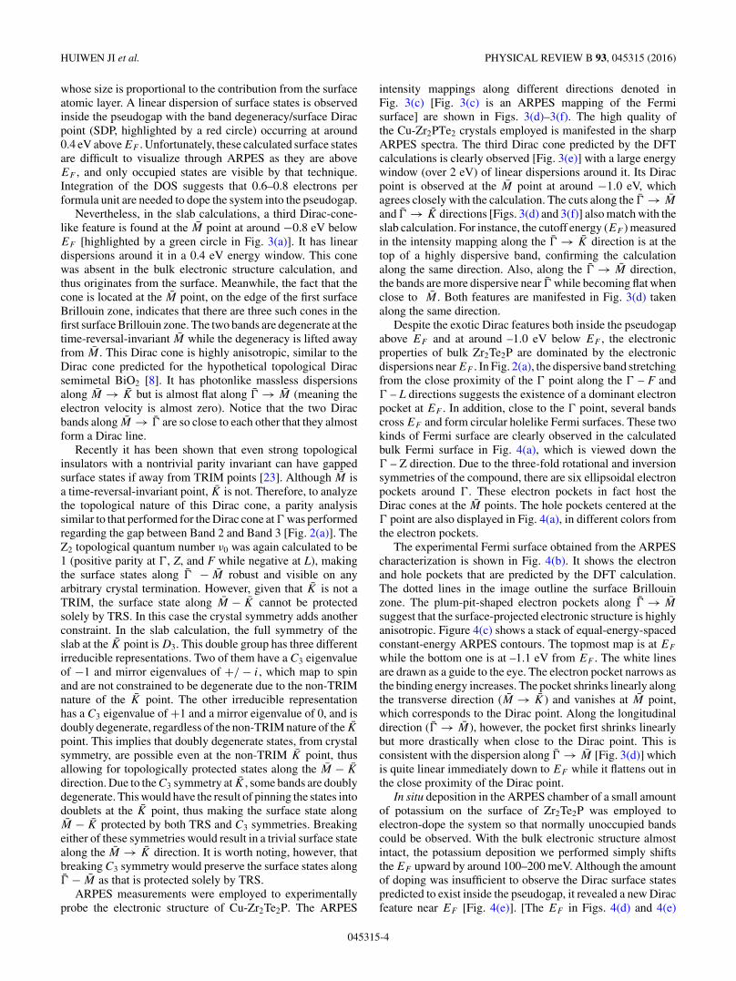
FIG. 3. (a) The slab electronic structure calculation that simulatesthe surface electronic structure. The band dispersions are plottedwith circles whose size is proportional to the contribution from thesurface atomic layer. Two topologically protected Dirac cones arehighlighted with a red and a green circle. (b) The rhombohedralBrillouin zone projects onto a hexagonal surface Brillouin zone. Allthe TRIMs are labeled. (c) Experimental ARPES intensity map of theFermi surface. The green arrows denote the high-symmetry directionsalong which the dispersion of Cu-Zr2Te2P bands was determinedby ARPES. These dispersions are shown in (d), (e), and (f), whichare cuts along the � − M , K− M−K , and K− �−K directions,respectively.
thus speculate that if EF can be tuned into the pseudogapthrough chemical doping or gating in Zr2Te2P, a surface-originated spin-polarized Dirac cone and a bulk-originatedspin-degenerate Dirac dispersion will come into play alongwith a few other bulk states. Although the transport will bedominated by bulk conduction, the Dirac-like dispersion ofthese bands might lead to high carrier mobility comparable tothat of other topological semimetals such as Cd3As2.
The bulk calculations that suggest the presence of atopologically protected Dirac cone on the surfaces of Zr2Te2Pat the � point agree closely with the slab calculation shownin Fig. 3(a), where an artificial unit cell is constructed bystacking five quintuple layers of Te-Zr-P-Zr-Te and putting avacuum space at the two ends. The slab calculation thereforepredicts the surface electronic structure on the (001) crystalface. Accordingly, the rhombohedral bulk Brillouin zoneis projected onto a hexagon-shaped surface Brillouin zone[Fig. 3(b)] where the four TRIMs collapse into � and M . In theslab calculation, the band dispersions are plotted with circles
045315-3
HUIWEN JI et al. PHYSICAL REVIEW B 93, 045315 (2016)
whose size is proportional to the contribution from the surfaceatomic layer. A linear dispersion of surface states is observedinside the pseudogap with the band degeneracy/surface Diracpoint (SDP, highlighted by a red circle) occurring at around0.4 eV above EF . Unfortunately, these calculated surface statesare difficult to visualize through ARPES as they are aboveEF , and only occupied states are visible by that technique.Integration of the DOS suggests that 0.6–0.8 electrons performula unit are needed to dope the system into the pseudogap.
Nevertheless, in the slab calculations, a third Dirac-cone-like feature is found at the M point at around −0.8 eV belowEF [highlighted by a green circle in Fig. 3(a)]. It has lineardispersions around it in a 0.4 eV energy window. This conewas absent in the bulk electronic structure calculation, andthus originates from the surface. Meanwhile, the fact that thecone is located at the M point, on the edge of the first surfaceBrillouin zone, indicates that there are three such cones in thefirst surface Brillouin zone. The two bands are degenerate at thetime-reversal-invariant M while the degeneracy is lifted awayfrom M . This Dirac cone is highly anisotropic, similar to theDirac cone predicted for the hypothetical topological Diracsemimetal BiO2 [8]. It has photonlike massless dispersionsalong M → K but is almost flat along � → M (meaning theelectron velocity is almost zero). Notice that the two Diracbands along M → � are so close to each other that they almostform a Dirac line.
Recently it has been shown that even strong topologicalinsulators with a nontrivial parity invariant can have gappedsurface states if away from TRIM points [23]. Although M isa time-reversal-invariant point, K is not. Therefore, to analyzethe topological nature of this Dirac cone, a parity analysissimilar to that performed for the Dirac cone at � was performedregarding the gap between Band 2 and Band 3 [Fig. 2(a)]. TheZ2 topological quantum number ν0 was again calculated to be1 (positive parity at �, Z, and F while negative at L), makingthe surface states along � − M robust and visible on anyarbitrary crystal termination. However, given that K is not aTRIM, the surface state along M − K cannot be protectedsolely by TRS. In this case the crystal symmetry adds anotherconstraint. In the slab calculation, the full symmetry of theslab at the K point is D3. This double group has three differentirreducible representations. Two of them have a C3 eigenvalueof −1 and mirror eigenvalues of +/ − i, which map to spinand are not constrained to be degenerate due to the non-TRIMnature of the K point. The other irreducible representationhas a C3 eigenvalue of +1 and a mirror eigenvalue of 0, and isdoubly degenerate, regardless of the non-TRIM nature of the K
point. This implies that doubly degenerate states, from crystalsymmetry, are possible even at the non-TRIM K point, thusallowing for topologically protected states along the M − K
direction. Due to the C3 symmetry at K , some bands are doublydegenerate. This would have the result of pinning the states intodoublets at the K point, thus making the surface state alongM − K protected by both TRS and C3 symmetries. Breakingeither of these symmetries would result in a trivial surface statealong the M → K direction. It is worth noting, however, thatbreaking C3 symmetry would preserve the surface states along� − M as that is protected solely by TRS.
ARPES measurements were employed to experimentallyprobe the electronic structure of Cu-Zr2Te2P. The ARPES
intensity mappings along different directions denoted inFig. 3(c) [Fig. 3(c) is an ARPES mapping of the Fermisurface] are shown in Figs. 3(d)–3(f). The high quality ofthe Cu-Zr2PTe2 crystals employed is manifested in the sharpARPES spectra. The third Dirac cone predicted by the DFTcalculations is clearly observed [Fig. 3(e)] with a large energywindow (over 2 eV) of linear dispersions around it. Its Diracpoint is observed at the M point at around −1.0 eV, whichagrees closely with the calculation. The cuts along the � → M
and � → K directions [Figs. 3(d) and 3(f)] also match with theslab calculation. For instance, the cutoff energy (EF ) measuredin the intensity mapping along the � → K direction is at thetop of a highly dispersive band, confirming the calculationalong the same direction. Also, along the � → M direction,the bands are more dispersive near � while becoming flat whenclose to M . Both features are manifested in Fig. 3(d) takenalong the same direction.
Despite the exotic Dirac features both inside the pseudogapabove EF and at around –1.0 eV below EF , the electronicproperties of bulk Zr2Te2P are dominated by the electronicdispersions near EF . In Fig. 2(a), the dispersive band stretchingfrom the close proximity of the � point along the � – F and� – L directions suggests the existence of a dominant electronpocket at EF . In addition, close to the � point, several bandscross EF and form circular holelike Fermi surfaces. These twokinds of Fermi surface are clearly observed in the calculatedbulk Fermi surface in Fig. 4(a), which is viewed down the� – Z direction. Due to the three-fold rotational and inversionsymmetries of the compound, there are six ellipsoidal electronpockets around �. These electron pockets in fact host theDirac cones at the M points. The hole pockets centered at the� point are also displayed in Fig. 4(a), in different colors fromthe electron pockets.
The experimental Fermi surface obtained from the ARPEScharacterization is shown in Fig. 4(b). It shows the electronand hole pockets that are predicted by the DFT calculation.The dotted lines in the image outline the surface Brillouinzone. The plum-pit-shaped electron pockets along � → M
suggest that the surface-projected electronic structure is highlyanisotropic. Figure 4(c) shows a stack of equal-energy-spacedconstant-energy ARPES contours. The topmost map is at EF
while the bottom one is at –1.1 eV from EF . The white linesare drawn as a guide to the eye. The electron pocket narrows asthe binding energy increases. The pocket shrinks linearly alongthe transverse direction (M → K) and vanishes at M point,which corresponds to the Dirac point. Along the longitudinaldirection (� → M), however, the pocket first shrinks linearlybut more drastically when close to the Dirac point. This isconsistent with the dispersion along � → M [Fig. 3(d)] whichis quite linear immediately down to EF while it flattens out inthe close proximity of the Dirac point.
In situ deposition in the ARPES chamber of a small amountof potassium on the surface of Zr2Te2P was employed toelectron-dope the system so that normally unoccupied bandscould be observed. With the bulk electronic structure almostintact, the potassium deposition we performed simply shiftsthe EF upward by around 100–200 meV. Although the amountof doping was insufficient to observe the Dirac surface statespredicted to exist inside the pseudogap, it revealed a new Diracfeature near EF [Fig. 4(e)]. [The EF in Figs. 4(d) and 4(e)
045315-4

STRONG TOPOLOGICAL METAL MATERIAL WITH . . . PHYSICAL REVIEW B 93, 045315 (2016)
FIG. 4. (a) DFT-calculated Fermi surface viewed down the � – Z direction in the first Brillouin zone. (b) Intensity mapping of theexperimental Fermi surface obtained from ARPES. The dotted lines in the image outline the boundaries of the surface Brillouin zone. (c) Astack of experimentally determined equal-energy-spaced constant-energy ARPES contours. The white lines are drawn as a guide to the eye. (d)The petal-like electron pockets were made to touch by electron doping of the bands. Constant-energy cuts show the shift of the band structureby some 150 meV. The red dotted line denotes where the electron pockets begin to touch. An energy-dependent mapping along this direction(parallel to M → K) is shown in (e).
represents the Fermi energy of n-doped Cu-Zr2Te2P, not theEF of the pristine compound in Figs. 4(b) and 4(c)]. From−0.2 eV to EF , the electron pockets begin to touch each otherat a point on the � − K azimuth. Here, the red dotted line inFig. 4(d) points to an azimuth that is parallel to the M → K
direction. The energy-dependent mapping along this directionis shown in Fig. 4(e). Two Dirac nodes are observed close tothe new EF . Since the two Dirac nodes are away from TRIMpoints and are not protected by any crystalline symmetry,spin-orbit coupling results in gapped Dirac points. We deducethat these massive Dirac nodes come from the slightly gappedbulk-derived Dirac dispersion inside the pseudogap [Fig.S1(right)]. The Dirac nodes are positioned at 0.6 eV abovethe pristine EF between M and K but lower in energy whentraveling away from M-K towards �, leading to a Dirac nodenear the new EF [shown in Fig. 4(e)]. Another Dirac-likecrossing at around −1.0 eV between the two massive Diracnodes in Fig. 4(e) corresponds to the extension of the Diracpoint along � → M . This crossing is not gapless due to thetiny splitting of the dispersion along � → M from the Diracpoint. These bands therefore also connect to the surface statescentered around M as discussed earlier.
IV. CONCLUSION
In conclusion, we have reported the discovery of a strongtopological metal, Zr2Te2P, where the band inversions are ofthe d-p type. Zr2Te2P adopts the same crystal structure asthe topological insulator Bi2Te2Se. It has two TRS-protectedsurface Dirac cones and one gapped 3D Dirac cone in itselectronic structure. The Dirac cone at the � point exists ina pseudogap at around 0.4 eV above EF , which is a result
of the band inversion between Zr 4d orbitals and Te 5p
orbitals. A second Dirac cone at the M point is derived froman electron pocket at EF , which shrinks when the energy islowered and vanishes to a doubly degenerate Dirac point at−1.0 eV. This Dirac cone is unusually anisotropic, with alinear dispersion along M → K but an almost flat, nearlydegenerate dispersion along � → M , similar in some ways tothe surface states observed in Ru2Sn3 [24], the nature of whichis still not understood. Unfortunately, the physical propertiesdue to the second Dirac cone are unlikely to be isolated dueto the coexistence of bulk bands in the same energy range.Nevertheless, this is apparently the first system to realize aTRS-protected Dirac cone at the M point although that waspredicted for the (111) surface of the Bi-Sb alloy system[25]. When EF is shifted upward through electron doping,the Dirac pockets touch each other on the � − K azimuth,forming a massive Dirac node gapped by spin-orbit coupling.We propose that if EF can be shifted into the pseudogap, it ispossible to realize high electron mobility and strong anisotropyin this system. Both chemical doping and gating are promisingmethods to realize this goal.
ACKNOWLEDGMENTS
The authors thank Lukas Muchler, Liang-Yan Hsu and BinLiu for helpful discussions. This work was supported by theARO MURI on topological insulators, Grant No. W911NF-12-1-0461. The ARPES measurements at the Advanced LightSource were supported by the U.S.Department of Energyunder Contracts No. DE-AC02-05CH11231 and No. DE-SC0012704.
045315-5

HUIWEN JI et al. PHYSICAL REVIEW B 93, 045315 (2016)
[1] T. Wehling, A. M. Black-Schaffer, and A. V. Balatsky, Adv.Phys. 63, 1 (2014).
[2] T. Liang, Q. Gibson, M. N. Ali, M. Liu, R. Cava, and N. Ong,Nat. Mater. 14, 280 (2015).
[3] J. Xiong, S. K. Kushwaha, T. Liang, J. W. Krizan, M.Hirschberger, W. Wang, R. Cava, and N. Ong, Science 350,413 (2015).
[4] Y. Chen et al., Science 325, 178 (2009).[5] H. Zhang, C.-X. Liu, X.-L. Qi, X. Dai, Z. Fang, and S.-C. Zhang,
Nat. Phys. 5, 438 (2009).[6] L. Fu, C. L. Kane, and E. J. Mele, Phys. Rev. Lett. 98, 106803
(2007).[7] L. Fu and C. L. Kane, Phys. Rev. B 76, 045302 (2007).[8] S. M. Young, S. Zaheer, J. C. Y. Teo, C. L. Kane, E. J. Mele,
and A. M. Rappe, Phys. Rev. Lett. 108, 140405 (2012).[9] M. Neupane et al., Nat. Commun. 5, 3786 (2014).
[10] Z. Liu et al., Nat. Mater. 13, 677 (2014).[11] Z. Liu et al., Science 343, 864 (2014).[12] Z. Ren, A. A. Taskin, S. Sasaki, K. Segawa, and Y. Ando, Phys.
Rev. B 82, 241306 (2010).[13] H. Ji, J. M. Allred, M. K. Fuccillo, M. E. Charles, M. Neupane,
L. A. Wray, M. Z. Hasan, and R. J. Cava, Phys. Rev. B 85,201103 (2012).
[14] K. Tschulik, M. Ruck, M. Binnewies, E. Milke, S. Hoffmann,W. Schnelle, B. P. T. Fokwa, M. Gilleßen, and P. Schmidt, Eur.J. Inorg. Chem. 2009, 3102 (2009).
[15] A. F. Kusmartseva, B. Sipos, H. Berger, L. Forro, and E. Tutis,Phys. Rev. Lett. 103, 236401 (2009).
[16] Y. S. Hor, A. J. Williams, J. G. Checkelsky, P. Roushan, J. Seo,Q. Xu, H. W. Zandbergen, A. Yazdani, N. P. Ong, and R. J. Cava,Phys. Rev. Lett. 104, 057001 (2010).
[17] See Supplemental Material at http://link.aps.org/supplemental/10.1103/PhysRevB.93.045315 for Table I, which contains thestructural characterization of Cu-Zr2Te2P, as well as Figs. S1and S2, which are the band structures of Zr2Te2P in a hexagonalBrillouin zone and the DOS of Zr2Te2P, respectively.
[18] D. J. Singh and L. Nordstrom, Planewaves, Pseudopotentials,and the LAPW Method (Springer Science & Business Media,New York, 2006).
[19] G. K. H. Madsen, P. Blaha, K. Schwarz, E. Sjostedt, and L.Nordstrom, Phys. Rev. B 64, 195134 (2001).
[20] E. Sjostedt, L. Nordstrom, and D. Singh, Solid State Commun.114, 15 (2000).
[21] J. Bland and S. Basinski, Can. J. Phys. 39, 1040 (1961).[22] M. Yang and W.-M. Liu, Sci. Rep. 4, 5131 (2014).[23] A. P. Weber, Q. D. Gibson, H. Ji, A. N. Caruso, A. V. Fedorov,
R. J. Cava, and T. Valla, Phys. Rev. Lett. 114, 256401 (2015).[24] Q. Gibson, D. Evtushinsky, A. N. Yarensko, V. B. Zabolotnyy,
Mazhar N. Ali, M. K. Fuccillo, J. Van den Brink, B. Buchner,R. J. Cava, and S. V. Borisenko, Sci. Rep. 4, 5168 (2014).
[25] J. C. Y. Teo, L. Fu, and C. L. Kane, Phys. Rev. B 78, 045426(2008).
045315-6