stretchable electronics: in‐plane deformation mechanics for...
TRANSCRIPT

STRETCHABLE ELECTRONICS
Scissoring/nonbuckling interconnects are proposed as a different route to stretchable structures, in which thick bar geometries replace thin ribbon layouts, to yield scissor-like/nonbuckling deformations instead of in or out of plane buckling, as discussed in article number 1604989 by Shuodao Wang, John A. Rogers, and co-authors. Metal and silicon structures with scissoring design can be stretched as much as 350% (previous maximum value 54%) and 90%, respectively, without fracture. Image designed by Zhenhai Li.
ADMA-29-8-Frontispiece.indd 2 04/02/17 9:53 PM

CO
MM
UN
ICATIO
N
© 2016 WILEY-VCH Verlag GmbH & Co. KGaA, Weinheim wileyonlinelibrary.com (1 of 12) 1604989
In-Plane Deformation Mechanics for Highly Stretchable Electronics
Yewang Su, Xuecheng Ping, Ki Jun Yu, Jung Woo Lee, Jonathan A. Fan, Bo Wang, Ming Li, Rui Li, Daniel V. Harburg, YongAn Huang, Cunjiang Yu, Shimin Mao, Jaehoun Shim, Qinglin Yang, Pei-Yin Lee, Agne Armonas, Ki-Joong Choi, Yichen Yang, Ungyu Paik, Tammy Chang, Thomas J. Dawidczyk, Yonggang Huang, Shuodao Wang,* and John A. Rogers*
DOI: 10.1002/adma.201604989
Prof. Y. SuState Key Laboratory of Nonlinear MechanicsInstitute of MechanicsChinese Academy of SciencesBeijing 100190, ChinaProf. Y. Su, Prof. Y. A. Huang, Prof. Y. HuangDepartment of Civil and Environmental Engineering and Department of Mechanical EngineeringNorthwestern UniversityEvanston, IL 60208, USAProf. Y. SuSchool of Engineering ScienceUniversity of Chinese Academy of SciencesBeijing 100049, ChinaProf. X. PingSchool of Mechanical EngineeringTianjin University of Science & TechnologyTianjin 300222, ChinaDr. K. J. Yu, Dr. J. W. Lee, Dr. D. V. Harburg, Dr. S. Mao, J. Shim, Q. Yang, P.-Y. Lee, A. Armonas, K.-J. Choi, Y. Yang, Dr. T. J. DawidczykFrederick Seitz Materials Research LaboratoryDepartment of Materials Science and EngineeringUniversity of Illinois at Urbana-ChampaignChampaign, IL 61820, USADr. J. W. Lee, U. PaikDepartment of Material Science and Engineering Department of Energy EngineeringHanyang UniversitySeoul 133-791, South Korea
Prof. J. A. Fan, T. ChangDepartment of Electrical EngineeringStanford UniversityStanford, CA 94305, USADr. B. Wang, Prof. S. WangSchool of Mechanical and Aerospace EngineeringOklahoma State UniversityStillwater, OK 74078, USAE-mail: [email protected] Dr. M. Li, Dr. R. Li, Prof. Y. SuState Key Laboratory of Structural Analysis for Industrial EquipmentDepartment of Engineering MechanicsDalian University of TechnologyDalian 116024, ChinaProf. Y. A. HuangState Key Lab Digital Manufacturing Equipment and Technology and Flexible Electronics Research CenterHuazhong University of Science and TechnologyWuhan, Hubei 430074, ChinaProf. C. YuDepartment of Mechanical EngineeringUniversity of HoustonHouston, TX 77204, USAProf. J. A. RogersDepartment of Electrical and Computer Engineering and the Department of Chemistry Beckman Institute for Advanced Science and TechnologyUniversity of Illinois at Urbana-Champaign, ChampaignUrbana, IL 61820, USAE-mail: [email protected]
Stretchable electronics represents a relatively recent class of tech-nology[1,2] of interest partly due to its potential for applications in sensory robotic skins,[3,4] conformal photovoltaic modules,[5,6] wearable communication devices,[7,8] skin-mounted monitors of physiological health,[9–11] advanced, soft surgical and clin-ical diagnostic tools,[11,12] and bioinspired digital cameras.[13,14] A key challenge in each of these systems is in the development of strategies in mechanics that simultaneously allow large levels of elastic stretchability and high areal coverages of active devices built with materials that are themselves not stretchable (e.g., conventional metals) and are, in some cases, highly brittle (e.g., inorganic semiconductors). For design approaches that embed stretchability in interconnect structures that join rigid device islands, the system level stretchability εsystem is much smaller than the interconnect stretchability εinterconnect. Zhang et al.[15]
identified the following relationship between the interconnect and system stretchability: (1 )system dev interconnectfε ε= − , where fdev = (area of active device components)/(total area of the system) is the areal coverage ratio of active device components. Struc-ture designs for stretchable interconnects have evolved from straight[13,16] to curvilinear interconnects,[17] from those bonded to or embedded in the supporting substrate[11,18] to free-standing designs housed in microfluidic enclosures,[19] and from simple structures[17] to fractal/self-similar designs.[15,20–22] All such cases, including a broad variety of shapes, sizes, and geometric arrangements, share the same underlying mechanisms, i.e., out-of-plane buckling of thin structures (metals, insulators, or semiconductors with thickness typically between ≈100 nm and ≈1 µm) provides the basis for elastic stretchability. The most advanced interconnects achieve elastic (reversible)
Adv. Mater. 2017, 29, 1604989
www.advancedsciencenews.com www.advmat.de

CO
MM
UN
ICATI
ON
© 2016 WILEY-VCH Verlag GmbH & Co. KGaA, Weinheimwileyonlinelibrary.com1604989 (2 of 12)
stretchability as high as ≈190%,[15] which corresponds only to ≈40% system stretchability when the areal coverage ratio is ≈60%. Lanzara et al.[23,24] introduced a design of networked microwires consisting of a thick layer of kapton film coated with a very thin layer of metal. These microwires can unfold in-plane, with linear response for stretching as large as 750%, and extendable for strains up to 1600%. The elastic stretcha-bility (defined here as the largest cyclic stretching that does not cause irreversible deformation or plastic strain) was, however, not explored in this work.[24] An additional limitation is that interconnects/antennas thin geometries have non-negligible electrical resistances and high levels of power dissipation.
This paper introduces a different route to stretchable struc-tures in which thick bar geometries replace thin ribbon layouts to yield scissor-like deformations instead of in- or out-of-plane buckling modes. Experiments and analytic/computational models show that metal and silicon structures with this bar type configuration can stretch to strains as large as 350% and 90%, respectively, without fracture. This is a significant improvement over previous studies that achieved ≈54% stretch-ability for pure-bending, narrow metal interconnects.[25] Metal features with these layouts have the additional advantage that they offer low resistance as interconnects for enhanced opera-tion in examples that include arrays of high-power LEDs and solar cells. In radio frequency (RF) antenna platforms, thick metal reduces RF losses and improves performance.
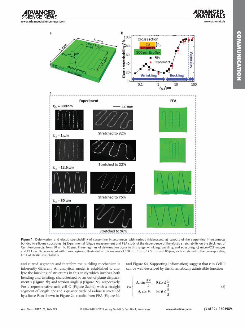
Experimental (see details in the Experimental Section) and finite element analysis (FEA) studies of the underlying mechanics focus on serpentine interconnects (see Figure 1a for the detailed layouts) made of copper, silicon, and polyimide (PI), with thickness/width aspect ratios between ≈1/1000 to ≈2.0. We used thicknesses between 50 nm and 80 µm for a fixed width of 45 µm here to focus the discussions. Studies shown in Figure S1 (Supporting Information) on interconnects with other widths show similar dependence on the thickness/width ratios. These interconnects feature very low electrical resist-ance (≈0.4 Ω), and the changes in resistance with stretching for all types of interconnects are less than a few percent up to the fracture points. In most applications, changes in this range have little practical importance. Investigations begin with copper interconnect traces fabricated on a thin layer PI and then transferred to an elastomer substrate (Ecoflex) as shown in Figure 1a,b. Systematic studies establish the following impor-tant aspects of this system:
(1) The existence of three distinct deformation modes: (a) wrinkling for very thin interconnects (sub-micrometer), as reported in prior studies[26,27] and also shown in Figure 1c for 300 nm and 1 µm; in this study, wrinkling is defined as out-of-plane buckling without significant twisting, with wavelength smaller than the length of the shortest straight segment (L/2 in Figure 1a); (b) coupled out-of-plane buck-ling and twisting with relatively long wavelengths (>L/2) for interconnects with moderate thickness (up to ≈45 µm), which we refer to as buckling and is shown in Figure 1c for 12.5 µm; similar transverse buckling behavior was observed in the study of Yang et al.;[28] (c) pure in-plane bending for even thicker interconnects (> ≈45 µm), which we call scis-soring (or non-buckling in comparison to previous studies
on buckling interconnects) as shown in Figure 1c for 80 µm. Detailed deformation of the three modes (amplitudes, wave-lengths, and twist angles) appear in Figure S2 (Supporting Information).
(2) A distinct dependence of the elastic stretchability of the inter-connects on thickness for a fixed width of 45 µm. The elastic stretchability corresponds to the largest cyclic stretching level that does not lead to microcracking in the interconnects. In FEA, elastic stretchability is defined as the largest stretch-ing level that does not cause yielding in the interconnects. The cyclic testing and FEA results are shown in Figure 1b. In the wrinkling regime (<≈2 µm), the elastic stretchabil-ity increases and then decreases with increasing thickness, with a maximum of ≈40% at a thickness of 200 nm.[29] In the buckling regime (2–50 µm), the elastic stretchability in-creases monotonically with the thickness, and then saturates at ≈100% when the thickness reaches ≈45 µm. The stretch-ability is independent of thickness in the scissoring regime (> 45 µm).
Transition from Wrinkling to Buckling: The mechanics of wrin-kling of a thin metal film on an elastomer substrate gives[22,26,27] the wavelength at the onset of wrinkling as
S
E2
4 int
sub
13
λ π≈
(1)
where subE is the plane-strain modulus of the substrate, and
4
12int
PI PI2
m m2 2
PI PI m m PI m2
PI PI m m
SE t E t E t E t t t
E t E t
( )( )
( )=
− + +
+
(2)
is the effective bending stiffness (per unit width) of the inter-connect, with tm and mE being thickness and plane-strain modulus of metal and tPI and PIE for PI, respectively. (See the Supporting Information for details.) A simple criterion for wrinkling is that the shortest straight segment of length L/2 (see Figure 1a) in the interconnect includes at least one wave-length, i.e.
/2Lλ < (3)
Equations (1)–(3) yield a critical metal thickness (see the Supporting Information for details):
tE
E
L34
crwrinkle-buckle sub
m
13
π≈
(4)
under the assumptions of ~PI metalt t and PI metalE E<< . Equation (4) separates wrinkling ( m cr
wrinkle-bucklet t< ) from buckling ( m cr
wrinkle-bucklet t> ). For Ecoflex with 49.3 kPasubE = , copper with 140 GPamE = ,[22] and L = 3 mm in experiments, Equation (4)
gives t 2.43 mcrwrinkle-buckle = µ , which agrees well with experiments
and FEA (Figure 1b,c and Figure S3, Supporting Information).Transition from Buckling to Scissoring: Although the coupled
bending/twisting instability of straight thin-wall bars has been well studied,[30] the scissoring structure here has both straight
Adv. Mater. 2017, 29, 1604989
www.advancedsciencenews.comwww.advmat.de
CO
MM
UN
ICATIO
N
© 2016 WILEY-VCH Verlag GmbH & Co. KGaA, Weinheim wileyonlinelibrary.com (3 of 12) 1604989
and curved segments and therefore the buckling mechanism is inherently different. An analytical model is established to ana-lyze the buckling of structures in this study which involves both bending and twisting, characterized by an out-of-plane displace-ment v (Figure 2b) and torsion angle φ (Figure 2c), respectively. For a representative unit cell ① (Figure 2a,b,d) with a straight segment of length L/2 and a quarter circle of radius R stretched by a force P, as shown in Figure 2a, results from FEA (Figure 2d,
and Figure S4, Supporting Information) suggest that v in Cell ① can be well described by the kinematically admissible function
sin , 02
cos , 02
0
0
vA
x
Lx
L
A
π
θ θ π=≤ ≤
≤ ≤
(5)
Adv. Mater. 2017, 29, 1604989
www.advancedsciencenews.com www.advmat.de
Figure 1. Deformation and elastic stretchability of serpentine interconnects with various thicknesses. a) Layouts of the serpentine interconnects bonded to silicone substrates. b) Experimental fatigue measurement and FEA study of the dependence of the elastic stretchability on the thickness of Cu interconnects, from 50 nm to 80 µm. Three regimes of deformation occur in this range: wrinkling, buckling, and scissoring. c) micro-XCT images and FEA results associated with these regimes, illustrated at thicknesses of 300 nm, 1 µm, 12.5 µm, and 80 µm, each stretched to the corresponding limit of elastic stretchability.

CO
MM
UN
ICATI
ON
© 2016 WILEY-VCH Verlag GmbH & Co. KGaA, Weinheimwileyonlinelibrary.com1604989 (4 of 12)
where the coordinates x and θ are defined in Figure 2a, and the buckling amplitude A0 is to be determined (Figure 2b). A periodic structure consists of four cells: Rotating cell ① by 180° around Axis AB (Figure 2d) gives cell ②; mirroring cells ① and ② about point C gives cells ③ and ④. Equilibrium gives the torque as /T Pv GJ xφ= − = ⋅∂ ∂ in the straight segment and
cos ( / ) /T Pv GJ Rθ φ θ= − = ⋅∂ ∂ in the curved segment, where GJ is the torsion stiffness. (Here the rotation ∂v/∂x is proportional
to A0/L and is approximated as zero for initial buckling.) This buckling mode has been verified by FEA (shown in Figure 2d, and detailed boundary conditions are discussed in the Sup-porting Information). Its integration, together with | 0/2φ =θ π= (verified in the FEA results in Figure 2d which shows φ reaches maximum at θ = 0 and vanishes at /2θ π= ), gives the analytic solution for φ (see the Supporting Information for details). Let wm and Em denote the width of the serpentine interconnect and
Adv. Mater. 2017, 29, 1604989
www.advancedsciencenews.comwww.advmat.de
Figure 2. Deformation mode in the buckling regime. a–c) Top-view, right-view, and cross-section view of Cell ①; d) deformation of an interconnect with thickness of 10 µm, viewed from the top, front, right, and at an angle.

CO
MM
UN
ICATIO
N
© 2016 WILEY-VCH Verlag GmbH & Co. KGaA, Weinheim wileyonlinelibrary.com (5 of 12) 1604989
the Young’s modulus of the metal, respectively, and /R Lα = . For an interconnect thickness of ≈10 µm, the effects of the soft substrate are negligible (see the Supporting Information and Figure S5). The energy method is used in the buckling analysis as the following: the potential energy Πbuckling, which is the sum of the torsional energy and energy for bending along the width and thickness directions subtracted by the work done by the external load P, is obtained in the Supporting Information as
2 4 2
3
16
1 1 3
2
1 1 5
96
buckling scissoring
202 2
02
2 1
402 5
2 5
2 1
604 7
4 7
P A
GJ
L P A R
GJ
EI EI
P A L
GJg
EI EI
P A L
GJg
π
α
α
( )
( )
( )
( )
Π = Π − −
− −
+ −
(6)
where
481 12 48 6scissoring
2 3
1
2 3P L
EIπα α πα( )Π = − + + + (7)
is the potential energy for the scissoring mode (see the Sup-porting Information for details), /121 m m m
3EI E t w= and /122 m m m
3EI E w t= are the bending stiffness along the width and thickness directions, respectively, and g5 > 0 and g7 > 0 are fifth- and seventh-order polynomials of α (see the Supporting Information for details). Minimization of Πbuckling with respect to A0, namely / 0bucklling 0A∂Π ∂ = , gives the following equation for A0
4316
1 1 3 1 1 5
2400
2 1
2 5
52 1
402 7
3 7π α α
( )( ) ( )⋅ + + −
− −
=AL R
EI EI
P L
GJg
EI EI
P A L
GJg
(8)
It should be noted here that Equation (8) only applies when P is greater than a certain critical buckling force Pcr > 0. The potential energies are then compared in the Supporting Information (Equations S14–S18). The buckling mode occurs only when it has lower energy than the scissoring mode, i.e., Πbuckling < Πscissoring. The result yields a criterion to separate buckling from scissoring as
crbuckling-scissoring
mt w= (9)
such that buckling and scissoring happen for tm < wm and tm ≥ wm, respectively (see the Supporting Information). This simple criterion also agrees well with FEA and experiments (Figure 1b).
In summary, the above analyses yields the following criteria for the three modes (also see a deformation map in Figure S6, Supporting Information)
t
w
E
E
L
w
E
E
L
w
t
wt
w
wrinkling if3
4
buckling if3
41
scissoring if 1
m
m
sub
m
13
m
sub
m
13
m
m
m
m
m
π
π
<
< <
<
(10)
Stretchability in the Wrinkling Mode: The maximum strain in the metal layer results mainly from out-of-plane bending during wrinkling, and is given by εmax = κmax d, where the max-imum curvature κmax depends on the applied strain (see the Supporting Information for details), and
2
2PI PI
2PI PI m m m
2
PI PI m m
dE t E t t E t
E t E t( )= + +
+
(11)
is the distance from the neutral mechanical plane to the top sur-face of the metal layer. The stretchability εstretchability is the applied strain when εmax reaches the yield strain εyield of the metal, and is determined from (see the Supporting Information for details)
134
2
44 /
2
stretchability stretchability
yieldint sub
1/3
PI PI m m
PI PI2
PI PI m m m2
S E E t E t
E t E t t E t
ε ε
ε( ) ( )
+
≈
++ +
(12)
where Sint is the effective bending stiffness given in Equation (1). The maximum stretchability is reached when the right hand side of Equation (12) attains its maximum, i.e., ()/ 0m∂ ∂ =t , which gives the optimal thickness m
optimumt of the metal as
moptimum
PI
PI
m
t
tf
E
E=
(13)
where the function f is given in the Supporting Information. For tm < tm
optimum, the stretchability increases with the metal thick-ness, and the opposite holds for tm > tm
optimum, which is consistent with Figure 1b. For 2.83GPaPI =E and tPI = 1.5 µm for PI,
140GPam =E for copper, Equation (13) gives moptimumt = 213 nm,
which agrees well with ≈200 nm obtained from FEA, as well as experimental results in Figure 1b.
Stretchability in the Buckling Mode: the experimental and FEA results in Figure 1b show that the stretchability of the buckling mode is a transition from low stretchability of the wrinkling mode to high stretchability of the scissoring mode. Compared to interconnects in the wrinkling and scissoring modes, buck-ling interconnects are much less attractive options for stretch-able electronics. Buckling interconnects are much thicker than wrinkling interconnects and therefore significantly decrease the overall flexibility of the system; on the other hand, they do not take full advantage of the scissoring mechanism to achieve optimum stretchability; out-of-plane twisting associated with the buckling mode also makes it undesirable for most practical designs. Therefore, we only focus on theoretical studies of the stretchability in the wrinkling and scissoring modes.
Stretchability in the Scissoring Mode: Only pure in-plane bending occurs in the scissoring mode. The elastic stretch-ability is the applied strain when the maximum strain, obtained analytically in the Supporting Information, reaches the yield strain εyield of the metal, which gives
w
L
w
L
1 12 48 6
23 1 2
stretchabilityscissoring
yield
2 3
m2
2m
ε ε πα α πα
α α( )= + + +
+ +
(14)
Adv. Mater. 2017, 29, 1604989
www.advancedsciencenews.com www.advmat.de

CO
MM
UN
ICATI
ON
© 2016 WILEY-VCH Verlag GmbH & Co. KGaA, Weinheimwileyonlinelibrary.com1604989 (6 of 12)
where α = R/L. This value is independent of the thickness and moduli of metal and substrate, which is confirmed by FEA as shown in Figure S7 (Supporting Information). For / 1mw L << (e.g., wm ≈ 0.01L in experiments), the elastic stretchability is linearly proportional to /yield mL wε ; it increases as the length L of the straight segment increases or the width wm deceases. This behavior occurs because, for the same in-plane rota-tion, a longer straight segment gives larger in-plane displace-ments to accommodate the stretching, while a smaller width wm reduces the in-plane bending strain which is linearly proportional to wm/2. For εyield = 0.3%,[31] the elastic stretcha-bility is shown in Figure 3a for various L and R, which agrees well with FEA for interconnect layouts and sizes identical to those in Figure 1a. The elastic stretchability, normalized
by /yield mL wε , is shown versus α = R/L in Figure 3b, which has a minimum at α = 0.60. For α < 0.60 as in all designs of interconnects presented here, the elastic stretchability increases as the radius R (or α) decreases. When L becomes very small or even approaches zero such as in S-shape inter-connects, Equation (14) reduces to (3 )/stretchability
S-shapeyield
2m2R wε πε= .
This realm of geometries falls outside of the scope of pre-sent studies but might be interesting to explore in future investigations. Fabrication of serpentine interconnects is most straightforward when the radius is at least twice the interconnect width wm.[32] Therefore, the minimum radius R = 2wm is used for LED and solar cell array structures to achieve largest stretchability, and Equation (14) then simpli-fies to /(12 )stretchability
scissoringyield
2m2ε ε= L w .
Adv. Mater. 2017, 29, 1604989
www.advancedsciencenews.comwww.advmat.de
Figure 3. a) Scaling law for the elastic stretchability of interconnects in the scissoring deformation mode. Analytical (solid lines) and FEA (dots) studies of the elastic stretchability of serpentine interconnects with various length L and radius R. b) Normalized elastic stretchability as a function of R/L. c) Experimental measurement of the stretchability of serpentine structures with silicon thickness ranging from 50 nm to 100 µm. c–d) Optical microscopy images of original (top frames) and fractured (bottom frames) serpentines with thicknesses of 300 nm (d) and 75 μm (e). f) The scissoring concept applied in encapsulation, prestrain, and fractal designs.
CO
MM
UN
ICATIO
N
© 2016 WILEY-VCH Verlag GmbH & Co. KGaA, Weinheim wileyonlinelibrary.com (7 of 12) 1604989
The scissoring concept can also be used to enhance the stretchability of brittle inorganic semiconductor materials such as silicon, as shown in Figure 3c–e. Here, stretchability of silicon was measured as the level of stretching (single cycle) that causes fracture in the interconnects. Both experiments (Figure 3c) and FEA (Figure S8 (Supporting Information) which shows the overall trend of stretchability vs thickness) confirm that the scissoring mode enhances the stretchability—thin ribbons that respond to applied force by wrinkling frac-ture at an applied strain of ≈30% (Figure 3d, bottom frames), while thick bars involve scissoring and break at a much higher applied strain of ≈90% (Figure 3e, bottom frames). Scissoring can also be exploited with previously demonstrated approaches in stretchable electronics such as dielectric encapsulation, fractal designs,[20,21,26] and prestrain strategies, as is shown in Figure 3f.[22,26] The structures shown in Figure S9a (Sup-porting Information) are encapsulated by a 500-µm-thick layer of silicone (Ecoflex, Smooth-On, Inc.). FEA results (Figure 3f, star markers) indicate that the encapsulation slightly lowers the stretchability for structures in the wrinkling or buckling regimes, but that it has almost no effect on the thick structures (>45 µm) in the scissoring regime. Here, the thick metal inter-connect is so much stiffer than the soft encapsulation layer that the encapsulation does not alter the deformation charac-teristics. Figure S9b (Supporting Information) shows a fractal serpentine interconnect, which replaces the straight segments in Figure 1a with curved segments that have a radii of curva-ture of 0.15 mm. This fractal design, when sufficiently thick (>45 µm) to promote the scissoring mode, enhances the elastic stretchability from 96% to 120% (Figure 3f, triangle markers). The fractal designs also take advantage of the scissoring thick interconnects placed in multiple directions, as a practical route toward multidirection deformation. Adoption of prestrain (Figure S9c, Supporting Information) can further improve the elastic stretchability. The prestrain should be restricted to values that, upon release, induce deformations within the elastic limit. Prestrain can increase the elastic stretchability of the scissoring structures (>45 µm) from 96% to 220% (Figure 3f, round markers).
Interconnects for Stretchable Arrays of LEDs: This demon-stration involves an optimized structure of copper (45 µm thickness; 45 µm width) for electrical interconnects between a collection of four LEDs supported by a thin silicone substrate (Ecoflex, 0.5 mm thickness) (see the Experimental Section for details). Figure 4a shows a functioning LED array in its original geometry and under 245% applied strain. Stretching beyond this level causes fracture of the substrate but not the inter-connects or their bonded interfaces to the LEDs. This level of stretchability is more than 2.5 times larger than that obtained with buckled structures in otherwise similar overall layouts.[33] The system remains functional after 20 000 cycles of stretching to 110%, as shown in the top left frame of Figure 4b. Similar cyclic testing to 120% leads to fractures at critical locations shown in the bottom and right frames of Figure 4b, consistent with FEA results shown in Figure 4c. This elastic stretchability, i.e. 110%, is three times larger than that previously obtained with wrinkling/buckling designs.[22,34] In addition to superior stretchability, the array also shows excellent electric/thermal performance, due to the large interconnect thickness (≈45 µm,
compared to traditional stretchable circuits of ≈300 nm). Both experimental and FEA results in Figure 4d and Figure S10 (Sup-porting Information) indicate that after 40 min of continuous operation at room temperature (24 °C), the LEDs reach thermal steady-state and maximum temperatures of only 82.5 °C at the LEDs and 68.3 °C at the interconnects (45 µm thickness). These values are much lower than those (201.6 °C at the LEDs and 131.8 °C at the interconnects) for the wrinkled system (≈300 nm thickness) under the same operational condition (Figure 4e). The thick interconnects have reduced resistances and therefore reduced power consumption by Joule heating; they also have increased effectiveness in heat dissipation.
Interconnects for Stretchable Arrays of Solar Cells: Compact, stretchable sources of power can be important for a range of applications. The thick metal layers with the scissoring design lead to interconnect resistances (45 µm thick, ≈0.4 Ω for each wire shown in the structure in Figure S11a, Supporting Infor-mation) that are much lower than those of thin, wrinkled struc-tures (e.g., 300 nm thick, ≈60 Ω for each wire). When integrated with solar cells, these low resistances are particularly important because they minimize parasitic power loss. Interconnects for a 2 × 2 array of solar cells (MicroLink Devices, dual junction GaAs/InGaP) on a silicone substrate yield a highly stretchable system (Figure 5a, top left frame).
Characterization of the mechanical and electrical per-formance involves bi-axial stretching while monitoring the current-voltage response under illumination with an AM 1.5 solar simulator. The results, shown in Figure 5b, indicate stable mechanical characteristics and invariant electrical per-formance with a short-circuit current of ≈−3.92 mA and an open-circuit voltage of ≈4.42 V, corresponding to an efficiency of ≈14.8% (computed based on the combined area of the solar cells). The efficiency of the solar cells remains constant for bi-axial stretching up to 110%. For stretching to 120%, the con-tact pads begin to delaminate (Figure 5b red curve in the inset and Figure 5c). This bi-axial elastic stretchability is more than ≈2 times larger than that achieved with buckled interconnects (60%).[35,36] The electroplated copper traces may have slightly different mechanical properties (e.g., yield strength) than those of the laser-milled samples. However, since the designed elec-troplated interconnects do not fracture during the testing, the effect of the difference in material properties is not discussed here. Although the scissoring mechanism is essentially for 1D stretching, it is observed here that multiple scissoring intercon-nects can be oriented in different directions, thereby providing a means to accommodate 2D stretching.
Traces for Stretchable RF Antennas: Radio frequency antennas are critical components of wireless communications and power delivery systems. To minimize resistive losses, the thickness of the metal traces should be significantly larger than the skin depth, which characterizes the penetration depth of electromag-netic waves in the metal. For copper at 1 GHz, the skin depth is ≈2 µm. Unlike traditional buckling approaches to stretch-able mechanics, which involve thicknesses of a few hundred nanometers, scissoring based schemes allow operation with thick structures.
Radio frequency dipole antennas constructed using the scissoring design consist of a mesh of enclosed metallic unit cells, each of which comprises four 1D interconnect patterns
Adv. Mater. 2017, 29, 1604989
www.advancedsciencenews.com www.advmat.de

CO
MM
UN
ICATI
ON
© 2016 WILEY-VCH Verlag GmbH & Co. KGaA, Weinheimwileyonlinelibrary.com1604989 (8 of 12)
(Figure 5d and Figure S12a and S13, Supporting Informa-tion). The dimensions of each unit cell (millimeter-scale) are much smaller than the operating wavelength (30 cm in free space at 1 GHz). As such, the mesh of unit cells can be treated as an effective metallic surface, in the form of an elec-tric metamaterial. We consider two different unit cell layouts:
one with three serpentine serpentine cycles on each unit cell side (Figure 5d) and one with a single serpentine cycle on each unit cell (Figure S12a, Supporting Information). From mechanical simulations, antennas with the single-serpentine layout can stretch to 32%, while antennas with additional ser-pentine cycles per cell can stretch to 40%. The stretchability of
Adv. Mater. 2017, 29, 1604989
www.advancedsciencenews.comwww.advmat.de
Figure 4. Demonstration of scissoring interconnects in a stretchable array of LEDs. a) Array of LEDs during operation in the original (left) and stretched (right) configurations. b) Array after cyclic testing to strains of 110% (top) and 120% (bottom). Fracture locations after cyclic testing to 120% strain appear in the frames on the right. c) FEA results for the strain distribution in the interconnect at stretching to 150%. d) Steady-state temperature distributions obtained from IR imaging and FEA for interconnects with thicknesses of 40 µm. e) Steady-state temperature distributions obtained from FEA for interconnects with thicknesses of 300 nm.

CO
MM
UN
ICATIO
N
© 2016 WILEY-VCH Verlag GmbH & Co. KGaA, Weinheim wileyonlinelibrary.com (9 of 12) 1604989Adv. Mater. 2017, 29, 1604989
www.advancedsciencenews.com www.advmat.de
these systems is larger than the 30% stretchability of previously reported designs[37] with 4-µm-thick copper wires due to the adoption of the scissoring physics.
The use of thick metal (30 µm) in these layouts leads to highly stretchable antennas. Testing involves soldering a 50 Ohm SMA cable at the antenna feed point and connecting it to a network analyzer for S11 return loss characterization.
The return loss spectra of the antennas at different levels of mechanical strain appear in Figure 5f. The design with three serpentine cycles has a resonance at 1.24 GHz at 0% strain, and 1.08 GHz upon 45% strain, compared to 1.5 GHz at 0% strain and 1.3 GHz upon 30% stretching for the design with a single serpentine cycle (Figure S12, Supporting Information). The resonance frequency of a linear dipole antenna scales inversely
Figure 5. Demonstration of scissoring interconnects in a stretchable array of solar cells and radio frequency dipole antennas. a) Solar cell arrays stretched bi-axially to various levels of strain (0%, 20%, 40%, 60%, 80%, and 110%). b) Current–voltage curves that correspond to these levels of stretching. c) Solar cells debonded from the contact pads due to biaxial stretching to ≈120%. d) Mechanical simulations of stretched antenna arms comprising unit cells with three serpentine cycles. e) Images of antennas bonded to an elastomer at different levels of strain. SMA cables soldered at the antenna feed points allow probing of the radiofrequency properties. f) Experimentally measured S11 return loss spectra for antennas with unit cells consisting of three serpentine cycles, under different strains. g) S11 return loss spectra by FEM simulations for antennas with unit cells consisting of three serpentine cycles, under different strains.

CO
MM
UN
ICATI
ON
© 2016 WILEY-VCH Verlag GmbH & Co. KGaA, Weinheimwileyonlinelibrary.com1604989 (10 of 12) Adv. Mater. 2017, 29, 1604989
www.advancedsciencenews.comwww.advmat.de
with the length of its arms, due to a combination of changes geometry and associated capacitive coupling. The reduction and narrowing of the S11 parameter as the antenna stretches results from enhanced impedance matching between the antenna and 50 Ohm SMA cable upon stretching. Radio frequency FEM simulations (see the Supporting Information for details) also display a strong dependence of antenna resonant frequency on mechanical strain. The antenna with three serpentine cycles in each unit cell resonates at 1.23 GHz at 0% strain, and 1.12 GHz at 40% strain (Figure 5g). The antenna consisting of a single serpentine cycle in each unit cell resonates at 1.52 GHz at 0% strain, and 1.29 GHz at 32% stretching (Figure S12d, Sup-porting Information). These theoretical results agree well with the experimental results shown in Figure 5d and Figure S12a (Supporting Information). Measurements of the S11 parameter of both antennas as a function of mechanical cycling is dis-played in Figure S14 (Supporting Information) and showed that as the antenna stretches and relaxes, there are no hysteresis effects and the resonant frequency and line shape are preserved.
The findings presented here demonstrate that scissor-like mechanics represents an important design approach that can complement previously reported schemes in stretchable electronics, where high elastic stretchability, high areal cover-ages of active devices, and high electric performance can be achieved simultaneously (by high performance, we refer to the low resistances and excellent thermal characteristics associated with thick interconnects.). More generally, systematic studies involving experimental work, FEA and analytical theory reveal three different deformation modes, wrinkling, buckling and scissoring, for serpentine structures of hard materials on soft elastomeric substrates. For otherwise comparable designs, the elastic stretchability in the scissoring regime is much higher than that in other two regimes. Analytical studies of these designs identify key geometric parameters that govern the elastic stretchability and yield optimal values for metallic ser-pentine interconnects that reach levels of stretchability up to 350%, roughly six times larger than previously reported values (≈60%)[22] when prestrain is not applied. The scissoring physics depends only on the thickness/width aspect ratio, and the stretchability is reversely proportional to the width. As a result, designs that involve thin interconnects with comparable (small) widths represent optimal options to achieve both large stretch-ability and large flexibility. Effects of encapsulation, fractal design layouts and prestrain strategy are studied systematically. The scissoring design also provides low electrical resistance and efficient heat dissipation in interconnect structures due to their thick geometries. Demonstrations include interconnects in arrays of high-power LEDs and high performance solar cells. Stretchable radio frequency antenna platforms illustrate the ability to reduce losses from skin-depth effects. The mechanics and technical approaches are distinct from those traditionally exploited in stretchable electronics, thereby providing some important, additional design options and technical capabilities.
Experimental SectionFabrication of Thin Metal Structures (<1 µm): Spin-casting yielded a
bilayer of poly(methyl methacrylate) (PMMA 495, MicroChem, at speed
of 3000 r.p.m. for 30 s, baked on a hotplate at 180 °C for 2 min) and a layer of PI (from poly(pyromellitic dianhydride-co-4,40-oxydianiline) amic acid solution; ≈1.5 µm, Sigma-Aldrich, 4000 r.p.m. for 40 s, baked on a hotplate at 150 °C for 5 min and then baked at 250 °C in vacuum for 1.5 h) on a silicon wafer. A layer of copper (300 nm, or 1.0 µm) was then deposited by electron beam evaporation onto the PI. Photolithography (AZ 4620) and etching (Type CE-100 copper etchant, Transene Company, at room temperature for ≈10 s) defined patterns in the metal layer. Next, oxygen plasma etching (180 mTorr, 20 sccm O2, 200 Watt for 20 min) patterned the PI in a geometry matched to the metal traces.
Immersion in hot acetone (80 °C) undercut the bottom PMMA layer, thereby allowing the entire structure to be retrieved from the silicon wafer onto the surface of a piece of water-soluble tape (3M). Electron beam evaporation of Cr (5 nm)/SiO2 (50 nm) formed backside coatings to enhance adhesion to a receiving substrate. Thin silicone slabs (Ecoflex ≈0.5 mm thick, Smooth-On) were prepared by mixing the two constituent components in a 1:1 weight ratio, casting the resulting material into a Petri dish and then partially curing it (17 h at room temperature and then 4 h at 70 °C). The surface of the silicone was treated with UV/Ozone for 4 min, and then the interconnect structures were transferred onto this surface with SiO2 facing down. The entire sample was immersed in water for 12 h to dissolve the water-soluble tape, thereby completing the fabrication processes.
Fabrication of Thick Metal Structures (>1 µm): Copper foils (Annealed Alloy 110, Electro Tough Pitch, smooth finish on both sides, All Foils Inc.) were laminated against a flat surface using water soluble tape (3M). A laser milling machine defined traces with designs determined by a CAD file. An infrared (wavelength 790–820 nm) laser with a power of 0.10 W and three sequential passes along the edges at a speed of 2.0 mm s−1 cut vertically through the copper foil (cross-section shown in Figure S15, Supporting Information). Excess material was removed after the laser milling and the desired traces were left on the flat water-soluble tape for ease of handling.
Electroplating of Thick Metal Structures (>45 µm, for the Solar Cell Array Samples): To fabricate the dense interconnecting traces for the solar cell array, accurate patterning was required and electroplating was adopted. Spin-casting defined a layer of poly(methyl methacrylate) (PMMA 495, MicroChem, at speed of 3000 r.p.m. for 30 s, baked on a hotplate at 180 °C for 2 min) on a silicon wafer. Seed layers of Ti (50 nm)/Cu (300 nm)/Ti (100 nm) were then deposited by electron beam evaporation onto the PMMA. Photolithographic exposure (NR21-20000P negative photoresist, Futurrex, 1500 rpm, 10 s) and development (RD6 developer, Futurrex, at room temperature for ≈8 min) defined a 60 µm thick mold on top of the metal layer (Figure S11b, Supporting Information), with desired wires and electrodes exposed. The Ti layer was then etched away using reactive ion etching (5 sccm O2, 10 sccm CF4, 300 mTorr, 200 W, ≈30 s) to expose the copper seed layer. Next, the wafer was connected to the negative terminal of a power supply and immersed into the electroplating bath (mixed from 900 mL H2O, 225 g cupric sulfate powder and 22.5 mL sulfuric acid). A copper sheet was connected to the positive terminal and immersed into the electroplating bath, aligned in parallel to the wafer. Passing a current density of 15 mA cm−2 for 3 h produced a low-resistive copper layer of 45 µm. The mold was then stripped with acetone and the exposed seed layers were removed by etching.
Immersion in hot acetone (80 °C) undercut the bottom PMMA layer, thereby allowing the entire structure to be retrieved from the silicon wafer onto the surface of a piece of water-soluble tape (3M). Electron beam evaporation of Cr (5 nm)/SiO2 (50 nm) formed backside coatings to enhance the adhesion to a receiving substrate. Thin silicone slabs (Ecoflex ≈0.5 mm thick, Smooth-On) were prepared with their surfaces treated with UV/Ozone for 4 min. The metal wires were transferred onto the silicone with SiO2 facing down. The entire sample was then immersed in water for 12 h to dissolve the water-soluble tape, thereby completing the fabrication processes. (Figure S11c, Supporting Information).
Fabrication of Silicon Structures: (1) Fabrication of thin serpentine Si ribbons (300 nm, 1.5 µm and 20 µm) began with patterning of ribbons

CO
MM
UN
ICATIO
N
© 2016 WILEY-VCH Verlag GmbH & Co. KGaA, Weinheim wileyonlinelibrary.com (11 of 12) 1604989Adv. Mater. 2017, 29, 1604989
www.advancedsciencenews.com www.advmat.de
and anchor structures on silicon-on-insulator wafers. Photolithography and inductive coupled plasma reactive ion etching (STS ICP RIE, STS Mesc Multiplex Advanced Silicon Etcher) of the top Si layers patterned Si ribbons with the necessary geometries. Immersion in hydrofluoric acid removed the buried oxide layer and isolated the serpentine Si ribbons from the bulk wafer, leaving small anchors that held the Si ribbons in place. The Si ribbons were then released from the anchors with a piece of water-soluble tape and transferred onto a thin silicon slab (Ecoflex ≈0.5 mm thick, Smooth-On). (2) For structures with thicknesses of 50 and 75 µm, the process began with spin-coating a layer of water-soluble adhesive (poly(vinyl alcohol) (PVA)) on a silicon wafer. Silicon thin films (University Wafers, double-sided cleaned and mirror finished) with thicknesses of 50 or 75 µm were then laminated on top of the PVA for ease of handling. Photolithography with a thick photoresist (AZ 4620, 1.2 µm) followed by inductively coupled plasma reactive ion etching (STS-ICPRIE) defined Si structures in the necessary geometries. The resulting structures were then transferred from the wafer to a thin silicon slab (Ecoflex ≈0.5 mm thick, Smooth-On). In the Si etching processes of (1) and (2), the STS ICPRIE parameters were adjusted according to the various thicknesses of the silicon films. For example, 80 cycles of etching were required to etch through 50 µm of Si, where each cycle involved a plasma deposition step and an etching step. Plasma deposition parameters were as follows: step time 4 s, inductively coupled plasma/platen power 600/0 W, C4F8 gas flow rate 110 sccm, pressure 94 mTorr. Etching parameters were as follows: step time 8 s, O2/SF6 gas flow rate 13/130 sccm, pressure: 94 mTorr, etching power 600/12 W.
Cyclic and Ultimate Tensile Strength Testing: Cyclic testing was performed with a Fexural Endurance Tester (CK Trade, Korea) at sets of 20 000 cycles at 5 Hz. To determine the elastic stretchability of each sample, the strain level was gradually increased until observation of the onset of microcracking. New samples tested under strains slightly lower than this value verified an elastic response, without cracking. Fracture testing was performed with a customized uniaxial stretcher. Optical microscope images allowed measurement of the elongation of each structure and to identify locations of fractures.
Supporting InformationSupporting Information is available from the Wiley Online Library or from the author.
AcknowledgementsY.S. acknowledges the support from Chinese Academy of Sciences via the “Hundred Talent program”, the National Science Foundation of China (NSFC, No. 11572323), and the State Key Laboratory of Structural Analysis for Industrial Equipment at Dalian University of Technology (No. GZ1603). X.P. acknowledges the support of NSFC (No. 51365013) and the Natural Science Foundation of Jiangxi Province of China through grant No. 20133ACB21002. J.W.L. and U.P. thank the GRL Program (K20704000003TA050000310) through the NRF funded by the Ministry of Science. S.W. acknowledges the support from the ASME Applied Mechanics Division-Haythornthwaite Foundation Research Initiation Grant, and partial support from the NSFC (Nos. 11272260, 11172022, 11572022, 51075327, and 11302038). Y.H. acknowledges the support from NSF (DMR-1121262, CMMI-1300846, CMMI-1400169, and IIP-1534120). J.A.R. acknowledges supports from the U.S. Department of Energy, Office of Science, Basic Energy Sciences, under Award # DE-FG02-07ER46741.
Received: September 16, 2016Revised: October 27, 2016
Published online: December 22, 2016
[1] J. A. Rogers, Nature 2010, 468, 177.[2] D. H. Kim, N. Lu, Y. Huang, J. A. Rogers, MRS Bull. 2012, 37, 226.[3] T. Someya, T. Sekitani, S. Iba, Y. Kato, H. Kawaguchi, T. Sakurai,
Proc. Natl. Acad. Sci. USA 2004, 101, 9966[4] M. Ramuz, B. C. K. Tee, J. B. H. Tok, Z. Bao, Adv. Mater. 2012, 24,
3223.[5] J. Lee, J. Wu, M. Shi, J. Yoon, S. I. Park, M. Li, Z. Liu, Y. Huang,
J. A. Rogers, Adv. Mater. 2011, 23, 986.[6] D. J. Lipomi, Z. Bao, Energy Environ. Sci. 2011, 4, 3314.[7] F. Axisa, P. M. Schmitt, C. Gehin, G. Delhomme, E. McAdams,
A. Dittmar, IEEE Trans. Inf. Technol. Biomed. 2005, 9, 325.[8] S. I. Park, Y. Xiong, R.-H. Kim, P. Elvikis, M. Meitl, D.-H. Kim, J. Wu,
J. Yoon, C. J. Yu, Z. Liu, Science 2009, 325, 977.[9] D. H. Kim, J. H. Ahn, W. M. Choi, H. S. Kim, T. H. Kim, J. Song,
Y. Y. Huang, Z. Liu, C. Lu, J. A. Rogers, Science 2008, 320, 507.[10] M. S. White, M. Kaltenbrunner, E. D. Głowacki, K. Gutnichenko,
G. Kettlgruber, I. Graz, S. Aazou, C. Ulbricht, D. A. Egbe, M. C. Miron, Nat. Photonics 2013, 7, 811.
[11] D. H. Kim, N. Lu, R. Ma, Y. S. Kim, R. H. Kim, S. Wang, J. Wu, S. M. Won, H. Tao, A. Islam, Science 2011, 333, 838.
[12] J. Viventi, D. H. Kim, J. D. Moss, Y. S. Kim, J. A. Blanco, N. Annetta, A. Hicks, J. L. Xiao, Y. G. Huang, D. J. Callans, J. A. Rogers, B. Litt, Sci. Transl. Med. 2010, 2, 24ra22.
[13] H. C. Ko, M. P. Stoykovich, J. Song, V. Malyarchuk, W. M. Choi, C. J. Yu, J. B. Geddes III, J. Xiao, S. Wang, Y. Huang, J. A. Rogers, Nature 2008, 454, 748.
[14] Y. M. Song, Y. Xie, V. Malyarchuk, J. Xiao, I. Jung, K. J. Choi, Z. Liu, H. Park, C. Lu, R. H. Kim, Nature 2013, 497, 95.
[15] Y. Zhang, S. Wang, X. Li, J. A. Fan, S. Xu, Y. M. Song, K. J. Choi, W. H. Yeo, W. Lee, S. N. Nazaar, B. Lu, L. Yin, K. C. Hwang, J. A. Rogers, Y. Huang, Adv. Funct. Mater. 2014, 24, 2028.
[16] Y. Su, J. Wu, Z. Fan, K. C. Hwang, J. Song, Y. Huang, J. A. Rogers, J. Mech. Phys. Solids. 2012, 60, 487.
[17] D. H. Kim, J. Song, W. M. Choi, H. S. Kim, R. H. Kim, Z. Liu, Y. Y. Huang, K. C. Hwang, Y. W. Zhang, J. A. Rogers, Proc. Natl. Acad. Sci. USA 2008, 105, 18675.
[18] C. H. Lee, Y. Ma, K. I. Jang, A. Banks, T. Pan, X. Feng, J. S. Kim, D. Kang, M. S. Raj, B. L. McGrane, B. Morey, X. Wang, R. Ghaffari, Y. Huang, J. A. Rogers, Adv. Funct. Mater. 2015, 25, 3698.
[19] S. Xu, Y. Zhang, L. Jia, K. E. Mathewson, K. I. Jang, J. Kim, H. Fu, X. Huang, P. Chava, R. Wang, S. Bhole, L. Wang, Y. J. Na, Y. Guan, M. Flavin, Z. Han, Y. Huang, J. A. Rogers, Science 2014, 344, 70.
[20] S. Xu, Y. Zhang, J. Cho, J. Lee, X. Huang, L. Jia, J. A. Fan, Y. Su, J. Su, H. Zhang, H. Cheng, B. Lu, C. Yu, C. Chuang, T. i. Kim, T. Song, K. Shigeta, S. Kang, C. Dagdeviren, I. Petrov, P. V. Braun, Y. Huang, U. Paik, J. A. Rogers, Nat. Commun. 2013, 4, 1543.
[21] Y. Su, S. Wang, Y. Huang, H. Luan, W. Dong, J. A. Fan, Q. Yang, J. A. Rogers, Y. Huang, Small 2015, 11, 367.
[22] J. A. Fan, W. H. Yeo, Y. Su, Y. Hattori, W. Lee, S. Y. Jung, Y. Zhang, Z. Liu, H. Cheng, L. Falgout, M. Bajema, T. Coleman, D. Gregoire, R. J. Larsen, Y. Huang, J. A. Rogers, Nat. Mater. 2014, 5, 3266.
[23] G. Lanzara, J. Feng, F. K. Chang, Smart Mater. Struct. 2010, 19, 045013.
[24] G Lanzara, N. Salowitz, Z. Q. Guo, F. K. Chang, Adv. Mater. 2010, 22, 4643.
[25] D. S. Gray, J. Tien, C. S. Chen, Adv. Mater. 2004, 16, 393.[26] D. Y. Khang, H. Q. Jiang, Y. Huang, J. A. Rogers, Science 2006, 311,
208.[27] H. Jiang, D. Y. Khang, J. Song, Y. Sun, Y. Huang, J. A. Rogers,
Proc. Natl. Acad. Sci. USA 2007, 104, 15607.[28] S. Yang, E. Ng, N. Lu, Extreme Mech. Lett. 2015, 2, 37.[29] This maximum exists because the interconnect is made of copper
and PI. For a single-layered material there is no maximum.[30] A. Gjelsvik, The Theory of Thin Walled Bars, Wiley, New York 1981.

CO
MM
UN
ICATI
ON
© 2016 WILEY-VCH Verlag GmbH & Co. KGaA, Weinheimwileyonlinelibrary.com1604989 (12 of 12) Adv. Mater. 2017, 29, 1604989
www.advancedsciencenews.comwww.advmat.de
[31] W. F. Riley, L. D. Sturges, D. H. Morris, Mechanics of Materials, Jon Wiley & Sons, New York 1999.
[32] P. Bartolo, J. Vasco, B. Silva, C. Galo, Assem. Autom. 2006, 26, 227.[33] R. H. Kim, M. H. Bae, D. G. Kim, H. Cheng, B. H. Kim, D. H. Kim,
M. Li, J. Wu, F. Du, H. S. Kim, Nano Lett. 2011, 11, 3881.[34] X. Ho, C. K. Cheng, R. L. S. Tan, J. Wei, J. Mater. Res. 2015, 30, 2271.
[35] J. Lee, J. Wu, J. H. Ryu, Z. Liu, M. Meitl, Y. W. Zhang, Y. Huang, J. A. Rogers, Small 2012, 8, 1851.
[36] S. Choi, H. Lee, R. Ghaffari, T. Hyeon, D. H. Kim, Adv. Mater. 2016, 28, 4203.
[37] A. M. Hussain, F. A. Ghaffar, S. I. Park, J. A. Rogers, A. Shamim, M. M. Hussain, Adv. Funct. Mater. 2015, 25, 6565.