strain, stress and cracks - u.s. pvmc module lifetime... · ... the key to combine ... undisturbed...
TRANSCRIPT
1 BROOKHAVEN SCIENCE ASSOCIATES
Strain, Stress and Cracks
Klaus Attenkofer PV Reliability Workshop (Orlando)
April 7-8, 2015
2 BROOKHAVEN SCIENCE ASSOCIATES
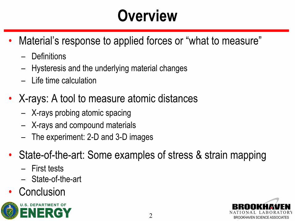
Overview • Material’s response to applied forces or “what to measure”
– Definitions – Hysteresis and the underlying material changes – Life time calculation
• X-rays: A tool to measure atomic distances – X-rays probing atomic spacing – X-rays and compound materials – The experiment: 2-D and 3-D images
• State-of-the-art: Some examples of stress & strain mapping – First tests – State-of-the-art
• Conclusion

3 BROOKHAVEN SCIENCE ASSOCIATES
Material’s Response to Applied Forces σ
= F/
A
ε = dl/l Strain:
Stre
ss:
Stress: Force per area (pressure)
Strain: Deformation due to stress
Elastic regime: Following Hooks law
Plastic regime: Not applicable to brittle materials
Strain hardening regime
http://www.mscsoftware.com/training_videos/patran/Reverb_help/index.html#page/Fatigue%2520Users%2520Guide/fat_theory.15.4.html
4 BROOKHAVEN SCIENCE ASSOCIATES
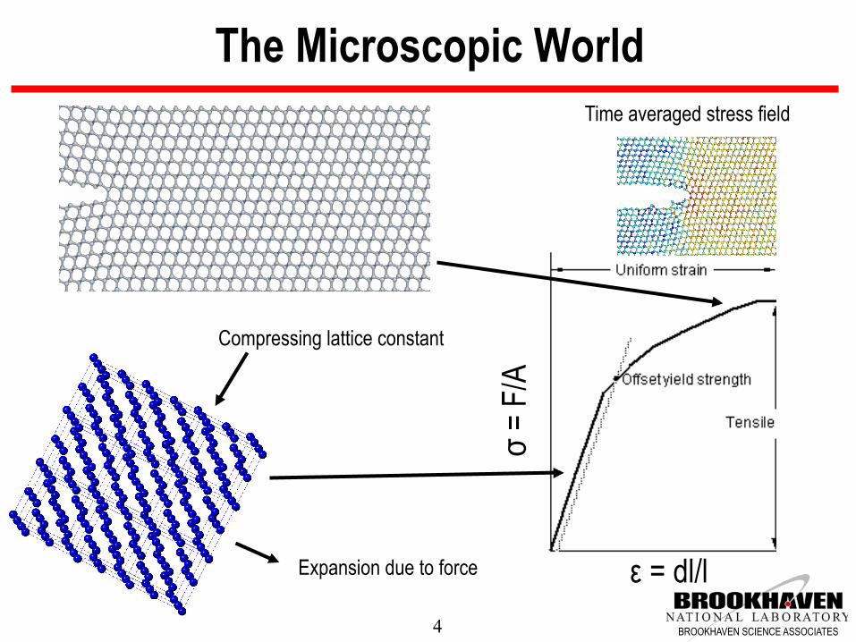
The Microscopic World
ε = dl/l σ
= F/
A
Time averaged stress field
Compressing lattice constant
Expansion due to force
5 BROOKHAVEN SCIENCE ASSOCIATES
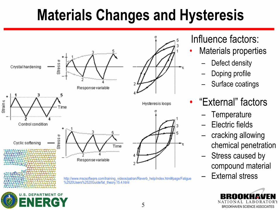
Materials Changes and Hysteresis
• Materials properties – Defect density – Doping profile – Surface coatings
• “External” factors – Temperature – Electric fields – cracking allowing
chemical penetration – Stress caused by
compound material – External stress
Influence factors:
http://www.mscsoftware.com/training_videos/patran/Reverb_help/index.html#page/Fatigue%2520Users%2520Guide/fat_theory.15.4.html
6 BROOKHAVEN SCIENCE ASSOCIATES
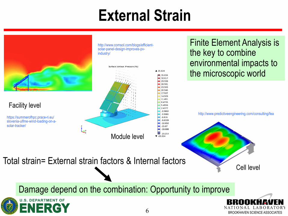
External Strain
Facility level
Module level
Cell level
Finite Element Analysis is the key to combine environmental impacts to the microscopic world
Total strain= External strain factors & Internal factors
Damage depend on the combination: Opportunity to improve
http://www.predictiveengineering.com/consulting/fea
http://www.comsol.com/blogs/efficient-solar-panel-design-improves-pv-industry/
https://summerofhpc.prace-ri.eu/slovenia-ulfme-wind-loading-on-a-solar-tracker/

7 BROOKHAVEN SCIENCE ASSOCIATES
Fracture: What to Measure
Crack Development
Curvature of wafer
Fracture
http://www.predictiveengineering.com/consulting/fea
lx
ε = dl/l
σ =
F/A
FEA σ = F/A
dl/l l of Reference/Standard
Mechanical properties
External force to bend

8 BROOKHAVEN SCIENCE ASSOCIATES
Lifetime Model / Performance
Distribution function of environmental stress factors
Mechanical response of panel
Crack development
Electrical performance at given time
Field data
FEA + ε = dl/l + Curvature of wafer
FEA + Spice-model

9 BROOKHAVEN SCIENCE ASSOCIATES
X-rays and Matter Scattering (photon in – photon out)
Photo-absorption (spectroscopy) Coherent scattering (Thomson)
Incoherent Scattering (Compton)
XAFS EXAFS
10 BROOKHAVEN SCIENCE ASSOCIATES
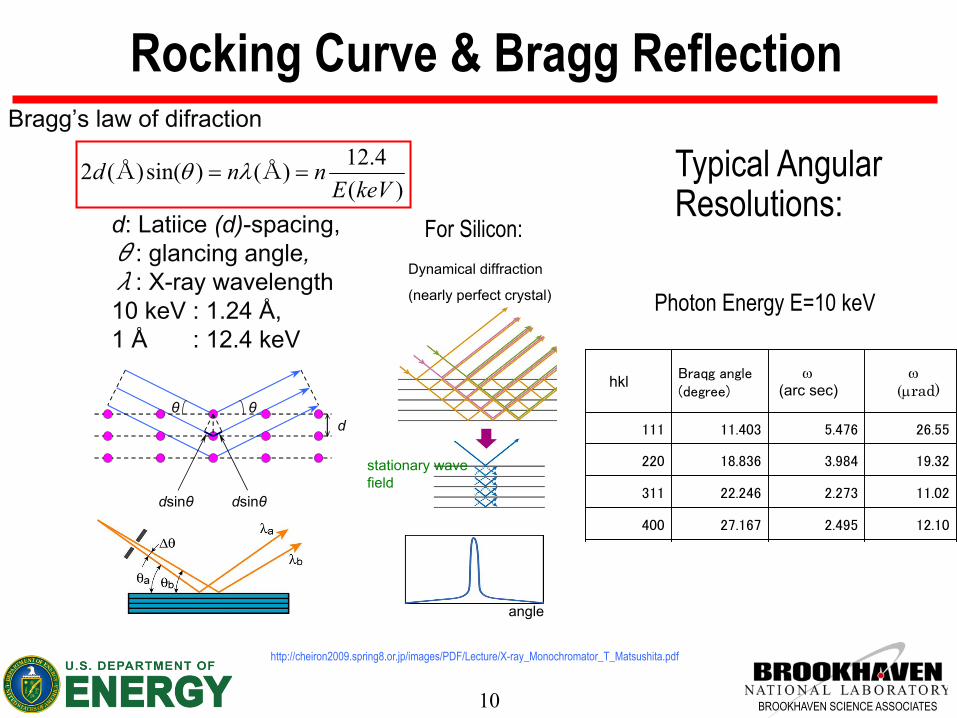
Rocking Curve & Bragg Reflection
Crystal monochromators
)(4.12)()sin()(2
keVEnnd ΈΈ OT
ș șd㩷
dsinș dsinș
TTOO cot'
'
'EE
d: Latiice (d)-spacing,㱔: glancing angle, 㱗: X-ray wavelength10 keV : 1.24 Å, 1 Å : 12.4 keV
Energy (wavelength) resolution
Higher harmonics
E1 = 10 keV (n = 1)
E2 = 20 keV (n = 2)
E3 = 30 keV (n = 3)
Bragg’s law of difraction
E1,E2,E3, 䊶䊶䊶䊶
X-ray diffraction by a single crystal
Kinematical diffraction
(imperfect crystal,
small crystal)
Dynamical diffraction
(nearly perfect crystal)
Single scattering
X-rays are scattered only once in the crystal.
Multiple scattering
Silicon
Germanium
Quartz
Diamond
gallium arsenide
stationary wave field
angleangle
Silicon single crystal, E = 10 keV
hkl 㪙㫉㪸㫈㪾 㪸㫅㪾㫃㪼㩿㪻㪼㪾㫉㪼㪼㪀
Z(arc sec)
� Z�� (Prad)
㪈㪈㪈 㪈㪈㪅㪋㪇㪊 㪌㪅㪋㪎㪍 㪉㪍㪅㪌㪌
㪉㪉㪇 㪈㪏㪅㪏㪊㪍 㪊㪅㪐㪏㪋 㪈㪐㪅㪊㪉
㪊㪈㪈 㪉㪉㪅㪉㪋㪍 㪉㪅㪉㪎㪊 㪈㪈㪅㪇㪉
㪋㪇㪇 㪉㪎㪅㪈㪍㪎 㪉㪅㪋㪐㪌 㪈㪉㪅㪈㪇
㪋㪉㪉 㪊㪋㪅㪇㪇㪈 㪈㪅㪏㪏㪍 㪐㪅㪈㪋㪉
㪊㪊㪊 㪊㪍㪅㪊㪎㪐 㪈㪅㪉㪉㪏 㪌㪅㪐㪌㪉
㪋㪋㪇 㪋㪇㪅㪉㪉 㪈㪅㪌㪋㪊 㪎㪅㪋㪎㪐
F0h on the web!!!
http://sergey.gmca.aps.anl.gov/x0h.html
Photon Energy E=10 keV
Crystal monochromators
)(4.12)()sin()(2
keVEnnd ΈΈ OT
ș șd㩷
dsinș dsinș
TTOO cot'
'
'EE
d: Latiice (d)-spacing,㱔: glancing angle, 㱗: X-ray wavelength10 keV : 1.24 Å, 1 Å : 12.4 keV
Energy (wavelength) resolution
Higher harmonics
E1 = 10 keV (n = 1)
E2 = 20 keV (n = 2)
E3 = 30 keV (n = 3)
Bragg’s law of difraction
E1,E2,E3, 䊶䊶䊶䊶
For Silicon:
Typical Angular Resolutions:
http://cheiron2009.spring8.or.jp/images/PDF/Lecture/X-ray_Monochromator_T_Matsushita.pdf
11 BROOKHAVEN SCIENCE ASSOCIATES
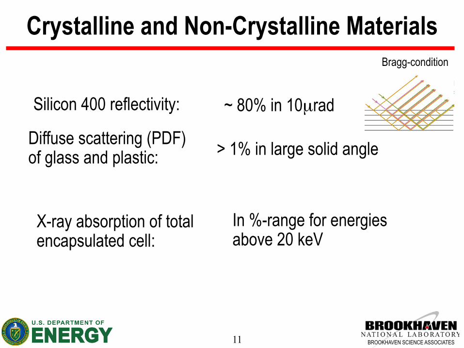
Crystalline and Non-Crystalline Materials
Silicon 400 reflectivity: ~ 80% in 10µrad
X-ray diffraction by a single crystal
Kinematical diffraction
(imperfect crystal,
small crystal)
Dynamical diffraction
(nearly perfect crystal)
Single scattering
X-rays are scattered only once in the crystal.
Multiple scattering
Silicon
Germanium
Quartz
Diamond
gallium arsenide
stationary wave field
angleangle
Bragg-condition
Diffuse scattering (PDF) of glass and plastic: > 1% in large solid angle
X-ray absorption of total encapsulated cell:
In %-range for energies above 20 keV

12 BROOKHAVEN SCIENCE ASSOCIATES
The Experimental Setup
Various information can be extracted:
http://www.phy.ncu.edu.tw/~CondensedLab/HRXRD.html
4-crystal setup provides monochromatic beam and “angular slit”
Sample can be measured in reflectivity (Bragg) or transmission mode (Laue)
Slit and detector can be replaced by area-detector (spatial resolution ~5µm)
• Orientation of the bragg-plane (curvature)in respect to x-ray beam: Rotation of sample to achieve bragg condition
• Lattice plane parameter l: angle of reflected beam • Strain:
Slit can be replaced by analyzer crystal to achieve high resolution with large (in scattering plane) beam
http://www.anka-cos.kit.edu/100.php

13 BROOKHAVEN SCIENCE ASSOCIATES
Crack Growth in Silicon
tilted platelets cleaved by the 50 N load. By measuring theaverage width of the X-ray image associated with the length ofcrack C2 into ½011" and comparing it with the calculatedtheoretical values for the crack widths from the differentdiffraction planes, it can be concluded that the crack runs fromdifferent (11l) planes into a predominantly ð112Þ plane. Someirregularities indicate conchoidal fracture. Since the criticalcrack lengths even for the narrowest images are greater thanthe wafer thickness, the cracks penetrate through to both sidesof the wafer, except the last 2.3 mm of the tip. This ending partof the tip is not visible either at the surface by NIC or in thebulk by infrared transmission light and therefore cannot beindexed, but {110} and {111} can be excluded. We thenexpected them to be visible in reflection XRDI as well as intransmission, and careful X-ray experiments on both sides ofthe wafer confirmed this to be the case. The crack C3 inFig. 2(b) appeared at relatively low temperature in the brittleregime of silicon in the perpendicular ½011" direction (compareFig. 1b). This crack starts again through complex high-indexedplanes capable of consuming much of the strain energy. Thenit deflects for a long distance into the low-energy ð011Þ planeuntil it ends in another more complicated plane which cannotbe indexed any more.
Fig. 3 shows a series of six topographs around the tip of thecrack C2. These images were taken from a movie of the wholeheating process, then image processed to improve the contrastand converted into false colours for improved visibility of the
contrast related to the strain fields. In Fig. 3(a), at roomtemperature before heating, a higher strain is visible at thecrack tip, indicated by the blue colours. This part of the crackbelow position P1 is inside the bulk of the wafer and notvisible at the surfaces (compare Figs. 4b and 4c). Directly afterheating, crack C2 opens and stops at position P1, about2.3 mm away from the visible sharp crack tip (Fig. 3b), whichcan be seen in images 0038–0048 on the video of the crackdevelopment. Obviously the opening of the crack appears onlyfor this part of the crack where the cleavage plane makes theconnection between the front and back side of the wafer. Inthe part of the crack that remains invisible below the surfaces,a long internal boundary line between the crack and theundisturbed crystal with a length of at least 4.6 mm results.Much more energy would be needed to elongate such a buriedcrack than the shortest direct connection, which would be, forexample, a straight h110i line with a length of only about1.0 mm between the wafers surfaces. Between images 0049 and0104 (corresponding to a temperature rise from 635 to 893 K)the opened crack remains at this position. During this period,for which the crack remains sessile, a substantial long-rangestrain field below P1 gradually builds up, visible as the dark-blue colours in Figs. 3(b)–3(e). Above P1 in parallel a muchhigher strain piles up in a very small volume S1, like a hot spotand into the ½001" direction, visible as the green–red colours.Another hot spot of strain S2 near the tip remains withoutconsequences during the experiment.
X-ray diffraction and imaging
852 Andreas Danilewsky et al. % Crack propagation and fracture in silicon wafers J. Appl. Cryst. (2013). 46, 849–855
Figure 2Transmission topographs of two cracks introduced from a 50 Nindentation at the wafer edge, 90& from the notch: Tc indicates theshadow of a thermocouple, P1 the position where crack C3 originates(room temperature, view from the back side through the sample). (a)Before the first heating sequence. The left crack C1 is short and shows asubstantial strain field at the tip of the crack for which ! = 20. The moredangerous crack C2 is almost four times longer and has a sharp contrast atthe tip; no strain field is visible which results in ! = 167. (b) After the firstheat treatment. The new horizontal crack C3 is generated. Around thecrack tips dense dislocations and slip bands were produced, visible fromthe black contrasts.
Figure 3False-coloured X-ray diffraction images around the tip of crack C2 (detailfrom Fig. 2a). (a) Image 0037 at room temperature before heating of thecrack C2. P1 marks the position where the opening of the crack isimpeded. (b) Image 0045 at '598 K (!T ’ 155 K). The image shows theopening crack which produces a huge strain field below P1 and a smallone S1 directly above. (c) Image 0049 at 689 K shows increasing strainfields, the upper one into the [001] direction. A small-sized strained areaS2 builds up near the tip. (d) Image 0060 at 788 K shows increasing strainat S1 above P1. (e) Image 0104 at 893 K. The strain fields below andabove P1 have both increased in size and intensity. The thermal stressexceeds 24.8 MPa. ( f ) Image 0105 at 895 K. The crack C3 has developedto the left into the [011] direction in less than 0.72 s and the strain fieldshave significantly decreased in size and intensity.
Before Heating After Thermal Cycling
tilted platelets cleaved by the 50 N load. By measuring theaverage width of the X-ray image associated with the length ofcrack C2 into ½011" and comparing it with the calculatedtheoretical values for the crack widths from the differentdiffraction planes, it can be concluded that the crack runs fromdifferent (11l) planes into a predominantly ð112Þ plane. Someirregularities indicate conchoidal fracture. Since the criticalcrack lengths even for the narrowest images are greater thanthe wafer thickness, the cracks penetrate through to both sidesof the wafer, except the last 2.3 mm of the tip. This ending partof the tip is not visible either at the surface by NIC or in thebulk by infrared transmission light and therefore cannot beindexed, but {110} and {111} can be excluded. We thenexpected them to be visible in reflection XRDI as well as intransmission, and careful X-ray experiments on both sides ofthe wafer confirmed this to be the case. The crack C3 inFig. 2(b) appeared at relatively low temperature in the brittleregime of silicon in the perpendicular ½011" direction (compareFig. 1b). This crack starts again through complex high-indexedplanes capable of consuming much of the strain energy. Thenit deflects for a long distance into the low-energy ð011Þ planeuntil it ends in another more complicated plane which cannotbe indexed any more.
Fig. 3 shows a series of six topographs around the tip of thecrack C2. These images were taken from a movie of the wholeheating process, then image processed to improve the contrastand converted into false colours for improved visibility of the
contrast related to the strain fields. In Fig. 3(a), at roomtemperature before heating, a higher strain is visible at thecrack tip, indicated by the blue colours. This part of the crackbelow position P1 is inside the bulk of the wafer and notvisible at the surfaces (compare Figs. 4b and 4c). Directly afterheating, crack C2 opens and stops at position P1, about2.3 mm away from the visible sharp crack tip (Fig. 3b), whichcan be seen in images 0038–0048 on the video of the crackdevelopment. Obviously the opening of the crack appears onlyfor this part of the crack where the cleavage plane makes theconnection between the front and back side of the wafer. Inthe part of the crack that remains invisible below the surfaces,a long internal boundary line between the crack and theundisturbed crystal with a length of at least 4.6 mm results.Much more energy would be needed to elongate such a buriedcrack than the shortest direct connection, which would be, forexample, a straight h110i line with a length of only about1.0 mm between the wafers surfaces. Between images 0049 and0104 (corresponding to a temperature rise from 635 to 893 K)the opened crack remains at this position. During this period,for which the crack remains sessile, a substantial long-rangestrain field below P1 gradually builds up, visible as the dark-blue colours in Figs. 3(b)–3(e). Above P1 in parallel a muchhigher strain piles up in a very small volume S1, like a hot spotand into the ½001" direction, visible as the green–red colours.Another hot spot of strain S2 near the tip remains withoutconsequences during the experiment.
X-ray diffraction and imaging
852 Andreas Danilewsky et al. % Crack propagation and fracture in silicon wafers J. Appl. Cryst. (2013). 46, 849–855
Figure 2Transmission topographs of two cracks introduced from a 50 Nindentation at the wafer edge, 90& from the notch: Tc indicates theshadow of a thermocouple, P1 the position where crack C3 originates(room temperature, view from the back side through the sample). (a)Before the first heating sequence. The left crack C1 is short and shows asubstantial strain field at the tip of the crack for which ! = 20. The moredangerous crack C2 is almost four times longer and has a sharp contrast atthe tip; no strain field is visible which results in ! = 167. (b) After the firstheat treatment. The new horizontal crack C3 is generated. Around thecrack tips dense dislocations and slip bands were produced, visible fromthe black contrasts.
Figure 3False-coloured X-ray diffraction images around the tip of crack C2 (detailfrom Fig. 2a). (a) Image 0037 at room temperature before heating of thecrack C2. P1 marks the position where the opening of the crack isimpeded. (b) Image 0045 at '598 K (!T ’ 155 K). The image shows theopening crack which produces a huge strain field below P1 and a smallone S1 directly above. (c) Image 0049 at 689 K shows increasing strainfields, the upper one into the [001] direction. A small-sized strained areaS2 builds up near the tip. (d) Image 0060 at 788 K shows increasing strainat S1 above P1. (e) Image 0104 at 893 K. The strain fields below andabove P1 have both increased in size and intensity. The thermal stressexceeds 24.8 MPa. ( f ) Image 0105 at 895 K. The crack C3 has developedto the left into the [011] direction in less than 0.72 s and the strain fieldshave significantly decreased in size and intensity.
Strain map during thermal cycling
RT 155C 400C
500C 600C
600C
Crack formation and relaxation of strain
J. Appl. Cryst. (2013). 46, 849–855

14 BROOKHAVEN SCIENCE ASSOCIATES
First Experiments at XPD (23ID)
7mm
5mm
Reflected beam in Laue geometry @ 34.5keV
Signal to Background: 26000/100
Mini-Module
0.02 degrees rotation between frames
Results: • Signal/Background ~300 • Bend of cell in wafer is 0.2 degrees • Setup needs to be improved to provide
strain analysis (easy task)

15 BROOKHAVEN SCIENCE ASSOCIATES
Proposed Setup at NSLS-II: 8-ID
Damping Wiggler Si-111 Si-220
Solar panel
Optional analyzer crystal
Area detector
• Beam parameters: • Photon energy: 20keV-36keV • Flux: 1013 Photon/s • Beam size: 80mm x 3mm
• Available beam time: 3x7days per week + x
IR-Camera
• Required time: • ~20min-25min per cell with 5-10µm
resolution • Detector readout determines time
• Number of cells per quarter year: ~2000
About: 3TB/hour!
16 BROOKHAVEN SCIENCE ASSOCIATES
Conclusion • Modified topography provides: • Curvature of PV cell within package • Locally resolved strain map (5-10µm resolution) • Signal/Background ratio is no problem • Perfect tool to provide input for simulation tools
• Expected throughput for optimized system: • About 20-30min per cell • About 1 full panel per day • 3 beamtimes with about (7+x) days available per year