stm32wb system power control - stmicroelectronics
TRANSCRIPT

Hello, and welcome to this presentation of the STM32WB power controller. Power management functions and all power modes will also be covered in this presentation.
1

STM32WB devices feature FlexPowerControl, which increases flexibility in power mode management and further reduces the overall application consumption. Run mode can support a system clock running at up to 64 MHz, with only 117 µA/MHz.STM32WB devices support 8 main low-power modes: Low-power run, Sleep, Low-power sleep, Stop 0, Stop 1, Stop 2, STANDBY with RAM retention, Standby and Shutdown SHUTDOWN modes. Each mode can be configured in many ways, providing several additional sub-modes. Note that for RF operation, the system cannot go bellow Standby with RAM retention mode as a minimum set of contexts needs to be maintained.In addition, STM32WB devices support a battery backup domain, called VBAT.The high flexibility in power management provides both high performance with a CoreMark score equal to 215, together with outstanding power efficiency, demonstrated by the
2

ULPBench score equal to 175.
.
2

The STM32WB has several key features related to power management:Several low-power modes, down to 30nA while it is still possible to wake up the MCU with an event on an I/O. For only 3200 nA, 32 Kbytes of SRAM can be retained. A large number of peripherals can wake up from the various low-power modes.Dynamic consumption is down to 77 µA/MHz, executing from Flash memory.A battery backup domain, called VBAT, including the RTC and certain backup registers.Several power supplies are independent, allowing to reduce MCU power consumption while some peripherals are supplied at higher voltages.Thanks to the large number of power modes, STM32WB devices offer high flexibility to minimize the power consumption and adjust it depending on active peripherals, required performance and needed wake-up sources.
3

STM32WB devices have several independent power supplies, which can be set at different voltages or tied together. The main power supply is VDD, supplying all I/Os, the reset block, temperature sensor and all internal clock sources. In addition, it supplies the Standby circuitry which includes the wakeup logic and independent watchdog as well as the Radio. VDD is monitored by the BORS circuitry. VDDSMPS supplies the Switch Mode Power Supply step-down converter. Its output VFBSMPS supplies the CPU with most of the digital peripherals and the SRAMs. The Flash memory is supplied by both VFBSMPS and VDD.STM32WB features several independent supplies for peripherals: VDDA for the analog peripherals, VDDUSB for the USB transceiver, VDDRF for the Radio. VLCD for LCD drivers, can be generated internally or come from an external supply.The internal Reference Voltage used by analog block can be
4

output on VREF+ pin to supply external circuitry for the application. A backup battery can be connected to the VBAT pin to supply the backup domain.
4

The SMPS supplies the digital core and radio LDOs.The SMPS supports switching on the fly. When the VDD supply drops below 2.1 V, it automatically switches to Bypass mode.The SMPS operating mode (on and off) will follow the device modes.To remove any noise from the SMPS during ADC conversions, software may switch on the fly the SMPS mode.
5

The STM32WB supply configuration is to be selected by hardware.For the best power performance, use the SMPS configuration.For the lowest cost, the LDO configuration can be used.
6

The main power supply VDD ensures full-featured operation in all power modes from 1.71 up to 3.6 V, allowing to be supplied by an external 1.8 V (+-5%) regulator. Device functionality is guaranteed down to 1.61 V, the minimum voltage after which a brown-out reset is generated. RF operation is allowed in the full voltage range from 1.71 to 3.6 V.Other independent supplies are provided to allow peripherals to operate at a different voltage.The VDDSMPS is connected to the same supply as VDD.The analog power supply VDDA can be connected to any voltage other than VDD. When the analog-to-digital converters or comparators are used, the VDDA voltage must be greater than 1.624 V. When the voltage reference buffer is used, VDDA must be greater than 2.4 V.The LCD Voltage can be generated internally or provided externally.The USB power supply VDDUSB can be connected to any
7
voltage other than VDD. When the USB is used, VDDUSB must be greater than 3 V. Note that three IOs of Port A[13 to 11], are supplied by VDDUSB independently from VDD.A backup domain is supplied by VBAT, which must be greater than 1.55 V. The backup domain contains the RTC, the 32.768-kHz LSE external oscillator and the 80-byte backup registers.
7

The power supply supervisor allows dynamic power supply management.STM32WB devices embed power management on main VDD, analog VDDA, VBAT supply input, Switch Mode Power Supply VFBSMPS, and USB interface VDDUSB supply lines.The main VDD supervision allows reset management and voltage detection via the power voltage detector (PVD) when VDD crosses the selected threshold. The PVD can be enabled in all modes except Standby modes. Seven thresholds can be selected by software. The Brown-out level can be used to provide switching on the fly of the SMPS when VDD drops below the threshold level.On the analog VDDA supply, a supervision circuit selected via PVM detects when VDDA crosses a threshold. The PVM can be enabled in all modes except Standby modes. On the VBAT supply, a supervision circuit selected via PVM detects when VBAT crosses a threshold. On the SMPS VFBSMPS supply, a supervision circuit will reset
8

the core when the supply is too low (<1.4 V).On the USB interface VDDUSB supply, ADC performs measurements to verify that the USB interface supply is present. The USB supply measurement can only be enabled in Run mode.
8

The power supply supervisor guarantees a safe and ultra-low power reset management.STM32WB devices embed an ultra-low-power brown-out reset (BOR) which is always enabled in all power modes except Shutdown mode. The BOR ensures reset generation as soon as the VDD drops below the selected threshold, regardless of the VDD slope. Five thresholds from 1.7 to 2.95 V are selected by option byte programmed in Flash memory.A power voltage detector can generate an interrupt when VDD crosses the selected threshold. The PVD can be enabled in all modes except Standby and Shutdown modes. Seven thresholds can be selected by software. In addition, an external pin can be used to compare voltages.The BOR consumption with the 1.7 V threshold is included in the datasheet.
9
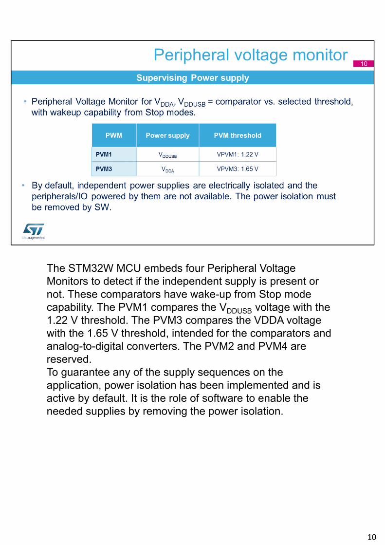
The STM32W MCU embeds four Peripheral Voltage Monitors to detect if the independent supply is present or not. These comparators have wake-up from Stop mode capability. The PVM1 compares the VDDUSB voltage with the 1.22 V threshold. The PVM3 compares the VDDA voltage with the 1.65 V threshold, intended for the comparators and analog-to-digital converters. The PVM2 and PVM4 are reserved.To guarantee any of the supply sequences on the application, power isolation has been implemented and is active by default. It is the role of software to enable the needed supplies by removing the power isolation.
10

The ADC and DAC voltage references can be provided either by an external supply voltage or by the internal reference buffer. This allows improvement of the converters performance by providing an isolated and independent reference voltage. The VREF+ pin and thus the internal voltage reference, is not available on the 48-pin package. In this package, the VREF+ is double-bonded with VDDA and the internal voltage buffer must be kept disabled. The voltage reference can be provided through the VDDA pin in this package.The application software can decide to place the SMPS in Bypass mode when performing ADC conversion to reduce noise.
11

The battery charging feature allows to charge a super-cap connected to VBAT pin through internal resistor when VDD
supply is present. The charging is enabled by software and is done either through a 5 kOhm or 1.5 kOhm resistor depending on software. Battery charging is automatically disabled in VBAT mode.
12

The STM32WB system contains three sub-systems. The CPU1 Cortex-M4, the CPU2 Cortex-M0+, and the Radio sub-system. Each of the three sub-systems can operate independently being in one of its operating modes CRun, CSleep, or CStop. Peripherals will only be clocked when the associated sub-system is in CRun mode, or CSleep when enabled in Sleep mode. The system resources such as RCC, PWR, AIEC and SRAM2, connected on the Shared bus will always be clocked when the system is in Run mode. The other peripherals on the Shared bus may be enabled to operate with CPU1 and/or CPU2. The SRAM1 and QSPI peripherals on the CPU1 bus matrix can only be associated with the CPU1 processor. The other CPU1 bus matrix peripherals may be enabled to operate with CPU1 and/or CPU2. The Radio system bus matrix can only be associated with the CPU2 processor. The Radio system BLE peripheral may operate when both CPUs are in CSleep and CStopmode, in this case only the system resources on the Shared
13

bus are clocked.
13

Each CPU can decide independently which low-power mode to use (Stop 0, Stop 1, Stop 2, Standby, or Shutdown).Each CPU can decide which IT source or RTC, RF (CPU2 only), GPIO signal, will wake it up.When both CPUs enter WFI (or WFE), the hardware mechanism executes the compatible request. It selects the highest low-power mode compatible with the requirements for both CPUs.One CPU can wake up without the need to wake up the other one if not required.When the STM32WB wakes up from Stop x modes, according with the Interruption source, only the CPU registered for this IT source is restarted, the other one stays in WFI (or WFE) with its clock stopped.When the STM32WB wakes up from Standby modes, in accordance with the source, only the CPU registered for this source is restarted, the other one stays under Reset mode.Run mode (Run Range 1, Run Range 2 and Low Power
14
Run) and Frequency selection changes are centralized on one of the CPUs to avoid conflicting configurations. This includes selection of the System clocks as well as LP enable and Voltage Range and Flash Memory configurations.
14

Each Radio sub-system operates autonomously and will enter and exit low-power modes on its own.The Radio low-power timer is the wakeup source for the Radio sub-system.When both CPUs and the Radio sub-system are in CStopmode, the system will enter the low-power mode as selected by the CPUs.
15

According to the requirements of the CPU1, CPU2 and RF systems, the PWR Hardware mechanism manages how the STM32WB reaches a given state. That is to say, when CPU1 allows Standby mode and CPU2 allows only Stop2 mode, the system enters Stop2 mode.Note that only the CPUs can place the system in LP Run or LP Sleep modes. The Radio does not support Shutdown mode and must be disabled prior to entering Shutdown mode.
16

Power management allows to control the device power supply based on system operating mode. The system operating mode depends on the individual CPUs and Radio operating modes. The system is in Run mode whenever one of the 3 sub-systems is in CRun or CSleep mode. The system enters Stop or Standby modes when all three sub-systems are in CStop mode.In system Run mode, the device power supply can be scaled according to the required performance: Up to 64 MHz in Range 1, 16 MHz in range 2, and only up to 2 MHz in low-power Run mode.
17

A CPU enters the CStop mode when executing a Wait for Interrupt (WFI) or Wait for Event (WFE) with the DEEPSLEEP bit set. The system state also depends on the operating modes of the other CPU and the radio system. The CPU1 bus matrix clock is only stopped when the other CPU has no allocated peripherals on the CPU1 clock domain or the other CPU is also in CStop mode. The system may only enter Stop or Standby mode when both the other CPU and the radio system are in CStop mode. The system only enters Standby mode when allowed by both CPUs.
18
When a CPU wakes up from its CStop mode, it has to know from which mode the domains and system have woken up. For this, the CPU has a few dedicated flag bits SBF_D1, SBF_D2, SBF and STOPF. These bits inform the CPU about the state of the system, and which parts (clock, peripherals) may need to be reinitialized.
19

These CxSBT (Standby) and CxSTOPF (Stop) flags have to be tested by the CPU software when waking up from Stop or Standby modes. They enable the CPU1 application to selectively reprogram its context (RAM, Peripherals and Clocks).
20

This figure gives the complete overview of the power modes in relation to the CPUs and Radio operating modes. Whenever a sub-system is in CRun or CSleep mode, the system is in Run mode. Low-power Stop, Standby and Shutdown modes are only entered when all three sub-systems are in CStop mode. The low-power mode is selected by the Low-Power Mode Select (LPMS) bits. Each CPU has its own Low-Power Mode select bits and the system enters the highest consuming low power mode selected. From Stop and Standby modes, each sub-system can be awakened independently by its own enabled wakeup sources. From Shutdown mode and Reset, only the CPU1 Cortex-M4 is awakened. It is up to the Cortex-M4 application software to wake up the CPU1 Cortex-M0+ and the Radio sub-system.
21

Each peripheral clock can be configured to be ON or OFF in Run and Low-power run modes. By default, all peripherals clocks are OFF, except the Flash interface clock. The SRAM1 and SRAM2 clocks are always ON in Run mode.When running from SRAM1 or SRAM2 (in Low-power run mode), the Flash memory can be put in Power-down mode thanks to software, and the Flash clock can be switched off. The Flash memory must not be accessed when it is switched off, consequently interrupts must be mapped in SRAM, using the CPU Vector Table Offset Register.
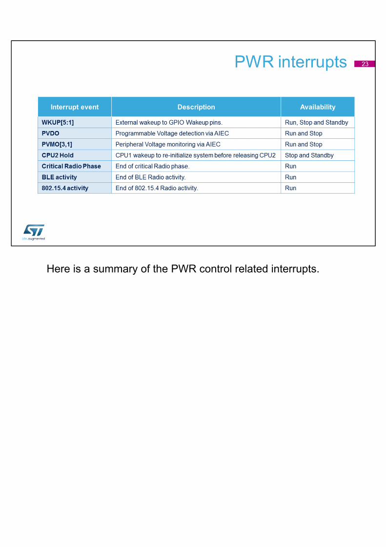
Here is a summary of the PWR control related interrupts.

Radio activity flags and interrupts are available to the Cortex-M4 and may be used to control the radio’s real-time operation, i.e. to prevent Flash memory operations from being executed during the radio’s critical phase.
24

The Run mode, thanks to voltage scaling, and the Low-power run modes offer flexibility between required performance and consumption.In Run mode range 1, the system clock is limited to 64 MHz and the internal and external oscillators and the PLL can be used. In Run mode range 2, the system clock is limited to 16 MHz and the internal and external oscillators as well as the PLL can be used, but must be limited to 16 MHz. In Low-power run mode, the system clock must be limited to 2 MHz.
Sleep and Low-power sleep modes allows all peripherals to be used and features the fastest wakeup time.In these modes, the CPU is stopped and each peripheral clock can be configured by software to be gated ON or OFF during the Sleep and Low-power sleep modes. These modes are entered by executing the assembler instruction Wait for Interrupt (WFI) or Wait for Event (WFE). When executed in Low-power run mode, the device enters Low-power sleep mode.Depending on the SLEEPONEXIT bit configuration in the Cortex M4 System Control Register, the MCU enters Sleep mode as soon as the instruction is executed, or as soon as it exits the lowest priority Interrupt Sub Routine. This last configuration allows you to save time and consumption by saving the need to pop and push the stack.

Batch Acquisition Mode is an optimized mode for transferring data. Only the needed communication peripheral + 1 DMA + SRAM1 or SRAM2 are configured with clock enable in Sleep mode.Flash memory is put in Power-down mode and the Flash memory clock is gated off during Sleep mode.Then it can enter either Sleep or Low-power sleep mode. Note that the I2C clock can be at 16 MHz even in Low-power sleep mode, allowing support for 1-MHz Fast-mode Plus. The USART and LPUART clocks can also be based on the high-speed internal oscillator. Typical applications are sensor hubs.
STM32WB devices features three Stop modes: Stop 0, Stop 1, and Stop 2, which are the lowest power modes with full retention and fast wakeup time to Run mode at maximum 48 MHz.The contents of SRAMs and all peripherals registers are preserved in all Stop modes.All high-speed clocks are stopped, except the ones used as kernel clock for peripherals capable of operating in Stop modes. The 32.768 kHz external oscillator and 32 kHz internal oscillator can be enabled.Several peripherals can be active and wake up from Stop mode.System clock on wake-up can be the internal high-speed and multi-speed oscillators up to 48 MHz, with only a 1 µs wakeup time from SRAM or 5 µs from Flash memory; add +10 µs when SMPS is used.Stop 2 consumption is lower than Stop 1 and 0, but supports

less active wakeup peripherals.
28

When comparing Stop modes:Stop 0 mode has the highest consumption as it keeps the Main Regulator ON.Stop 1 mode consumption is higher than Stop 2 mode consumption, but the wakeup time is shorter and the number of active peripherals is higher.It is possible to wake up from Stop 0 or 1 mode with the USB Resume from Suspend event or with Attach Detection, but it is not supported in Stop 2 mode.
The I2C address recognition is functional in both Stop modes, and can generate a wakeup event in case of an address match. Only 1 I2C is supported in Stop2 versus 2 I2Cs in other Stop modes.The UART byte reception is functional in both Stop modes and can generate a wakeup event in case of Start detection or Byte reception or Address match event. Only the low-power UART is supported in Stop2 mode. In other Stop
29

modes, all UARTs and the low-power UART can generate a wakeup event.When clocked by the internal or external low-speed oscillator, or when clocked by an external pin, the low-power timer can wake up the MCU with all its events. In Stop 0 and Stop 1 modes, both low-power timers are supported whereas only LPTIM1 is supported in Stop 2 mode.
29
To allow the CPU1 to re-initialize the clock system when exiting from Stop modes, the Stop hold function holds the CPU2 until the CPU1 has re-initialized the system. To ensure this, a wake-up from Stop mode interrupt holds the CPU2 and wakes up the CPU1 with a wake-up hold interrupt. Oncethe CPU1 has re-initialized the system, it releases the CPU2 hold.
30

The Standby mode is the lowest power mode in which 32 Kbytes of SRAM2 can be retained, the automatic switch from VDD to VBAT is supported and the I/Os level can be configured by independent pull-up and pull-down circuitry.By default, the voltage regulators are in Power down mode and the SRAMs and the peripherals registers are lost. The 80-byte backup registers are always retained. The ultra-low-power brown-out reset is always ON to ensure a safe reset regardless of the VDD slope. Each I/O can be configured with or without a pull-up or pull-down, which is applied and released thanks to the APC control bit. This allows control of the inputs state of external components even during Standby mode.The Radio IP can wake up the CPU2.Five wakeup pins are available to wake up both CPUs from Standby mode. The polarity of each of the five wakeup pins is configurable.The wakeup clock is HSI with a frequency of 16MHz.
31

Shutdown mode is the lowest power mode of the STM32WB, with only 30 nA at 1.8 V.This mode is similar to Standby mode but without any power monitoring: the brown-out reset is disabled and the switch to VBAT is not supported in Shutdown mode. The LSI is not available, and consequently the independent watchdog is also not available. A brown-out reset is generated when the device exits Shutdown mode: all registers are reset except those in the backup domain, and a reset signal is generated on the pad.The 80-byte backup registers are retained in Shutdown mode.The wakeup sources are the 5 wakeup pins and the RTC.When exiting Shutdown mode, the wakeup clock is MSI at 4 MHz.
32

The backup domain allows us to keep the RTC functional and to preserve the backup registers in case the VDD supply is down, thanks to a backup battery connected to the VBAT pin.The backup domain contains the RTC clocked by the low-speed external oscillator at 32.768 kHz. Three tamper pins are functional in VBAT mode, and will erase the 80-byte backup registers also included in the VBAT domain, in case of intrusion detection.The backup domain also contains the RTC clock control logic.In case VDD drops below a certain threshold, the backup domain power supply automatically switches to VBAT. When VDD is back to normal, the backup domain power supply automatically switches back to VDD . The VBAT voltage is internally connected to an ADC input channel in order to monitor the backup battery level.When VDD is present, the battery connected to VBAT can be
33

charged from the VDD supply.
33

Here you can see the summary of all the STM32WB powermodes.
34

Three bits are available in the Flash option bytes to prohibit a given low-power mode. When cleared, an option bit configures reset generation when entering Shutdown mode. Another bit configures reset generation when entering Standby mode and the last bit configures reset generation when entering Stop 1 or Stop 2 modes.One bit is used to configure the behavior of the BORHxthreshold, either as a reset (as in STM32L4 family) or to automatically switch the SMPS into Bypass mode. Note that switching back to SMPS mode when VDD increases depends on the application.
35
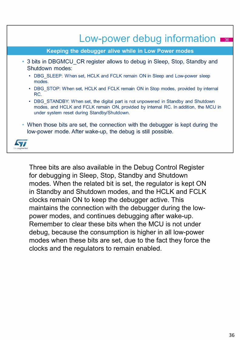
Three bits are also available in the Debug Control Register for debugging in Sleep, Stop, Standby and Shutdown modes. When the related bit is set, the regulator is kept ON in Standby and Shutdown modes, and the HCLK and FCLK clocks remain ON to keep the debugger active. This maintains the connection with the debugger during the low-power modes, and continues debugging after wake-up. Remember to clear these bits when the MCU is not under debug, because the consumption is higher in all low-power modes when these bits are set, due to the fact they force the clocks and the regulators to remain enabled.
36

In addition to this training, you can refer to the Reset and Clock Control, Interrupts trainings as well as those for all the peripherals with wakeup from Stop and Standby capability.
37