stinfo copy - dtic · report documentation page form approved omb no. 0704-0188 public reporting...
TRANSCRIPT

APPROVED FOR PUBLIC RELEASE; DISTRIBUTION UNLIMITED.
STINFO COPY
AIR FORCE RESEARCH LABORATORY INFORMATION DIRECTORATE
OPTICAL INFORMATION SCIENCE
September 2011 Final Technical Report
ROME, NY 13441 UNITED STATES AIR FORCE AIR FORCE MATERIEL COMMAND
AFRL-RI-RS-TR-2011-221

NOTICE AND SIGNATURE PAGE Using Government drawings, specifications, or other data included in this document for any purpose other than Government procurement does not in any way obligate the U.S. Government. The fact that the Government formulated or supplied the drawings, specifications, or other data does not license the holder or any other person or corporation; or convey any rights or permission to manufacture, use, or sell any patented invention that may relate to them. This report was cleared for public release by the 88th ABW, Wright-Patterson AFB Public Affairs Office and is available to the general public, including foreign nationals. Copies may be obtained from the Defense Technical Information Center (DTIC) (http://www.dtic.mil). AFRL-RI-RS-TR-2011-221 HAS BEEN REVIEWED AND IS APPROVED FOR PUBLICATION IN ACCORDANCE WITH ASSIGNED DISTRIBUTION STATEMENT. FOR THE DIRECTOR: /s/ /s/ RICHARD MICHALAK, Technical Advisor MICHAEL HAYDUK, Acting Chief Computing and Communications Division Information Directorate This report is published in the interest of scientific and technical information exchange, and its publication does not constitute the Government’s approval or disapproval of its ideas or findings.

REPORT DOCUMENTATION PAGE Form Approved OMB No. 0704-0188
Public reporting burden for this collection of information is estimated to average 1 hour per response, including the time for reviewing instructions, searching data sources, gathering and maintaining the data needed, and completing and reviewing the collection of information. Send comments regarding this burden estimate or any other aspect of this collection of information, including suggestions for reducing this burden to Washington Headquarters Service, Directorate for Information Operations and Reports, 1215 Jefferson Davis Highway, Suite 1204, Arlington, VA 22202-4302, and to the Office of Management and Budget, Paperwork Reduction Project (0704-0188) Washington, DC 20503. PLEASE DO NOT RETURN YOUR FORM TO THE ABOVE ADDRESS.1. REPORT DATE (DD-MM-YYYY)
September 2011 2. REPORT TYPE
Final Technical Report 3. DATES COVERED (From - To)
January 2008 – September 2010 4. TITLE AND SUBTITLE OPTICAL INFORMATION SCIENCE
5a. CONTRACT NUMBER In House
5b. GRANT NUMBER N/A
5c. PROGRAM ELEMENT NUMBER62702F
6. AUTHOR(S) Joseph Osman, Michael Fanto, Thomas McEwen, Clare Thiem, Jared Pawloski, Andrew Corp, Cory Johnson, David Huber
5d. PROJECT NUMBER OPIS
5e. TASK NUMBER 00
5f. WORK UNIT NUMBER 01
7. PERFORMING ORGANIZATION NAME(S) AND ADDRESS(ES)Air Force Research Laboratory/Information Directorate Rome Research Site/RITC 525 Brooks Road Rome, NY 13441-4505
8. PERFORMING ORGANIZATION REPORT NUMBER N/A
9. SPONSORING/MONITORING AGENCY NAME(S) AND ADDRESS(ES)Air Force Research Laboratory/Information Directorate Rome Research Site 26 Electronic Parkway Rome NY 13441
10. SPONSOR/MONITOR'S ACRONYM(S) AFRL/RI/RRS
11. SPONSORING/MONITORING AGENCY REPORT NUMBER AFRL-RI-RS-TR-2011-221
12. DISTRIBUTION AVAILABILITY STATEMENT Approved for Public Release; Distribution Unlimited. PA# 88ABW-2011-1859. Date Cleared: 29 March 2011
13. SUPPLEMENTARY NOTES
14. ABSTRACT The purpose of this in-house program was to develop techniques, architectures and systems in optical information science to support AF programs in advanced computer concepts and signal processing. We concentrated on bringing optical interconnects1 into advanced architectures as a way of reducing latency in interprocessor communications, especially at the memory level. We began by exploring free space interconnection and designed a selective receiver to allow high signal-to-noise interconnects with low power emitters on processors. In parallel, we researched ways of optically interconnecting a fielded computational cluster where the processors were PS3 commodity computers that use the Cell Broadband Engine (CBE). Later we helped the Wireless Computational Network Architecture (WCNA) program with optical interconnects to act as backup systems in the case of RF jamming, act as very short range interconnects where RF intermodulation distortion did not allow use of wireless and as a way of connecting wireless computational cluster nodes separated by long distances. 15. SUBJECT TERMS Optical interconnects, computational clusters, wireless networks, free space optical links
16. SECURITY CLASSIFICATION OF: 17. LIMITATION OF ABSTRACT
UU
18. NUMBER OF PAGES
40
19a. NAME OF RESPONSIBLE PERSON JOSEPH OSMAN
a. REPORT U
b. ABSTRACT U
c. THIS PAGE U
19b. TELEPHONE NUMBER (Include area code) N/A
Standard Form 298 (Rev. 8-98) Prescribed by ANSI Std. Z39.18

Table of Contents List of Figures……………………………………………………………………………………. iii List of Tables…………………………………………………………………………………….. iii 1 SUMMARY ................................................................................................................................. 1 1 INTRODUCTION .................................................................................................................... 1
1.1 Current research ............................................................................................................... 1 1.2 Our research direction ...................................................................................................... 2
FREE-SPACE PROCESSOR TO PROCESSOR INTERCONNECTS ......................................... 3 2 SUMMARY ............................................................................................................................. 3 3 INTRODUCTION .................................................................................................................... 3 4 METHODS, ASSUMPTIONS, AND PROCEDURES ........................................................... 3 5 RESULTS AND DISCUSSION .............................................................................................. 4 6 CONCLUSIONS ...................................................................................................................... 4 INTERCONNECTS FOR A PS3 CLUSTER ................................................................................. 4 7 SUMMARY ............................................................................................................................. 4 8 INTRODUCTION .................................................................................................................... 4 9 METHODS, ASSUMPTIONS, AND PROCEDURES ........................................................... 5
9.1 Approach .......................................................................................................................... 5 9.2 Mapping out of the PS3 hardware .................................................................................... 5 9.3 Best insertion points for optical interconnect ................................................................... 7
10 RESULTS AND DISCUSSION .......................................................................................... 8 10.1 Investigation of USB Latency .......................................................................................... 8 10.2 Design of prototype optical interconnect system. ............................................................ 9 10.3 Further testing ................................................................................................................ 10
11 CONCLUSIONS................................................................................................................ 10 INTERCONNECTS FOR WIRELESS COMPUTATIONAL NETWORKS .............................. 11 12 SUMMARY ....................................................................................................................... 11 13 INTRODUCTION ............................................................................................................. 12 14 METHODS, ASSUMPTIONS, AND PROCEDURES ..................................................... 12
14.1 Short Range Option ........................................................................................................ 12 14.2 Medium and Long Range Options ................................................................................. 13
15 RESULTS AND DISCUSSION ........................................................................................ 14
i

15.1 Short Range Option ........................................................................................................ 14 15.2 Medium and Long Range Options ................................................................................. 16
15.2.1 Simple Link Testing ................................................................................................ 16 15.2.2 Collimator Testing .................................................................................................. 17 15.2.3 Free Space Optical Propagation Range ................................................................... 18 15.2.4 Node to Node testing .............................................................................................. 19
16 CONCLUSIONS................................................................................................................ 19 17 PROGRAM CONCLUSIONS ........................................................................................... 22
19 REFERENCES ............................................................................................................... 24
20 APPENDIX A “A MIMO-Inspired Rapidly Switchable Photonic Interconnect Architecture” 26
ii

LIST OF FIGURES Figure 1. 60 MHz PS3 Motherboard (top) 6 Figure 2. Initial Interconnect Setup 9 Figure 3. Second Interconnect Setup 10 Figure 4. USB to IrDA IR2000UL; Ruggedized USB to IrDA IR220LR 13 Figure 5. Optical Media adapters, Collimator 14 Figure 6. IrDA Pattern Measurement Setup 14 Figure 7 IR2000UL Range Pattern (in meters) 15 Figure 8. IR220LR (ruggedized) Range Pattern (in meters) 15 Figure 9. Experimental Enclosure for 5 Picoboard Node 16 Figure 10. Regular Use Of Media Converters 16 Figure 11. Free Space Optical Link Configuration 17 Figure 12. Bandwidth Measurement 17 Figure 13. Media Converter & Collimator; Camera & Laser Beam Analyzer 18 Figure 14. Two Node Setup 19 Figure 15. Cluster to Cluster Communications 20 Figure 16. Future System 21 Figure 17. SkyFiber unit. 22 Figure 18. Low Impact Plasmonic EO Conversion 23
LIST OF TABLES Table 1. USB Results 8 Table 2. Some Short Range Interconnect Options 12
iii
1 SUMMARY The purpose of this in-house program was to develop techniques, architectures and systems in optical information science to support AF programs in advanced computer concepts and signal processing. We concentrated on bringing optical interconnects1 into advanced architectures as a way of reducing latency in interprocessor communications, especially at the memory level. We began by exploring free space interconnection and designed a selective receiver to allow high signal-to-noise interconnects with low power emitters on processors. In parallel, we researched ways of optically interconnecting a fielded computational cluster where the processors were PS3 commodity computers that use the Cell Broadband Engine (CBE). Later we helped the Wireless Computational Network Architecture (WCNA) program with optical interconnects to act as backup systems in the case of RF jamming, act as very short range interconnects where RF intermodulation distortion did not allow use of wireless and as a way of connecting wireless computational cluster nodes separated by long distances. The funding for this work was salary only but we were able to get some supplies and equipment funds for individual items from Dr. Linderman and Dr. Suter.
1 INTRODUCTION
1.1 Current research Clock speed is no longer the prime figure of merit for speed of computation. The end of Moore’s Law seems to be in sight and the increase in logic switching speed has slowed considerably. However, there is too much latency associated with standard interconnects and intracomputer communication. Interconnection delay and thermal effects are now the prime chip speed limiting factors, interconnection wires are already as close as possible and the interconnection delay is already close to the gate delay. Manufactures have been going to multi-core processors instead and speed of inter-processor communications is the new figure of merit.
General purpose processors will run out of space for pins for interprocessor communication in about five years. For this reason, manufacturers such as IBM, Intel and Sun have begun work on optical interconnects as a solution to this problem. Their schemes typically use a few wavelengths in each channel to increase information density without adding additional electronic pins. The optical interconnect system is kept in a single layer over or below the processors.
Current interconnection schemes are based on packet switching and do not give a direct connection between processors. There are several routing paradigms being used. In Manhattan routing, addresses in headers are read after conversion to electronic form at each intersection of the switching fabric and a decision that requires a clock cycle or two to properly route the packet to its eventual destination is made. In broadcast and select routing a message is broadcast to all
Approved for Public Release; Distribution Unlimited 1

other addresses in parallel and only the proper destination accepts the packet after it converts the header to electronic form. These current approaches have limited reconfigurability and suffer from poor latency. This makes it hard to tightly couple and synchronize processors.
1.2 Our research direction Some form of richer and smarter interconnects will be required in military special purpose processors to speed computation. Poor latency is what keeps users from fully enjoying the speedup of parallel processing. Some communication/computation operations inherent in parallel computing are not very amenable to the speedup that parallel processing gives most other operations. These include cache coherency subsystems and aggregators in scatter-gather operations. We need to look at ways to target these operations that are not being efficiently performed in parallel for hardware speedup. Also, we need to look at how to interconnect advanced computing architectures that are still in the research stage. These architectures typically will need richer and smarter interconnects in order to replace the current conventional computing architectures for specialized computing. Meanwhile, we can still leverage developments from these large commercial optical interconnect programs. Another aspect of the current optical interconnect architectures is that they are using a smaller size version of an old idea – that of the optical link. In an optical link, electronic data is converted to optical form and used to modulate a laser. This laser light goes through some channel and arrives at a detector, where it is converted back into electronic form. There are several ways that this can be modified. First, the optics can use free space for the transmission channel. Then there is no need for fiber or waveguide and decision making within the transmission channel. Instead, some initial processing and a pointing system is needed to send the data along an optical beam to its proper destination. Second, non-invasive optical sensing techniques as used in high speed optical testing of electronic circuits could be used to convert the electronic data into optical data without the use of a laser and/or a modulator on the electronic chip itself. The laser could be in the optical interconnect layer. This could dramatically decrease the power and real estate needs of the electronic processor chip. Third, optically addressed electronic memory could be used to put data directly from an optical interconnect into electronic memory. This would be especially fitting for memory-to-memory interconnect systems to perform cache coherence. Fourth, planar all-optical methods could be used to read addresses / packet headers and redirect the data streams to the proper address using all-optical switching. This would require some means of performing optical level restoration and optical processing. This processing could initially be done in a bit serial fashion just like an electronic computer but using optical components. This would lower latency by eliminating optical-to-electronic conversion, which takes time. Processing required in smarter networks may be the initial target for this.
Approved for Public Release; Distribution Unlimited 2

FREE-SPACE PROCESSOR TO PROCESSOR INTERCONNECTS
2 SUMMARY Past research here in Rome in interconnecting stacked planar computing layers showed the difficulty of achieving low latency in that type of architecture. In conversations with Dr. Richard Linderman, Senior Scientist for Advanced Computing Architectures, we discussed free space interconnects as a possible new approach. We decided to see if versatile interconnects for multi-core HPC could best be performed using free-space interconnects between spherically or cylindrically arranged processors. In the past we worked on optical methods of beamforming and beamsteering of RF signals with Dr. Henry Zmuda of the University of Florida. After discussing this with him, he suggested that we use a 2-D MIMO inspired spatially selective receiver with a phased array electronically steered aperture for the free-space optical interconnect. We brought him in as a summer professor and he designed such a system.
3 INTRODUCTION The goal of using phased array techniques for aperturing laser light has been unattainable so far because the techniques used in RF require that the array elements be at most equal to ½ the wavelength, which has not been possible with the nm-scale wavelengths of light. Greater separation than ½ wavelength (λ/2) leads to unwelcome grating lobes, destroying the angular selectivity of the system. However, MIMO techniques have been used in RF systems to produce more compact higher resolution and higher sensitivity steerable apertures for such things as cell tower antennas. In MIMO systems multiple different waveforms called diversity waveforms are used. Using these techniques allows sparser arrays to perform as well or even better than conventional λ/2 arrays. Steering the receiver aperture lowers the power requirements of the emitters on the processor chips by achieving a high signal-to-noise (S/N) channel only for the selected emitter. By using an array of radiators, one per processor, an increase in total radiated power is achieved, while greatly relieving the power burden on a single laser. The diversity requirement can be attained by making each processor emit light at a different wavelength. This is practical because the International Telecommunications Union (ITU) has standardized a set of wavelengths (the ITU grid) for wavelength division multiplexing (WDM) and commercially available lasers are available for these wavelengths.
4 METHODS, ASSUMPTIONS, AND PROCEDURES See Appendix A – “A MIMO-Inspired Rapidly Switchable Photonic Interconnect Architecture” published in Proceedings of the SPIE, Volume 7339.
Approved for Public Release; Distribution Unlimited 3

5 RESULTS AND DISCUSSION See Appendix A – “A MIMO-Inspired Rapidly Switchable Photonic Interconnect Architecture” published in Proceedings of the SPIE, Volume 7339.
6 CONCLUSIONS The analysis presented and illustrated by simulation shows that even for arrays with element spacing greater that the usual half-wavelength, significant advantages are realized. The diversity approach utilized here, namely the use of multiple laser wavelengths, results in a significant amplitude reduction at all angles except that of the main lobe. Tradeoffs among the various system parameters would produce a design that has been optimized for a particular interconnect application.
INTERCONNECTS FOR A PS3 CLUSTER
7 SUMMARY The objective of this project was to research alternative methods of connecting the AFRL/RRS PS3 cluster together. The current configuration uses 1GigE to connect the Playstation 3s (PS3s) to each router (forming a subcluster), and InfiniBand to connect the subclusters together into the main routing network. There is an inherently large overhead associated with Ethernet, which is combined with the limitations imposed on the (Fedora Core 7 Linux) operating system’s control of the Ethernet port by the Hypervisor, which acts as an emulation layer between the PS3 hardware and the Linux environment. Retrofitting a commercial system made for consumer use will be difficult, but more cost effective than buying custom blade systems with Cell processors and multiple I/O ports.
8 INTRODUCTION The problem we will target occurs in Parallel Discrete Event Simulation (PDES)2, used in the Air Force for modeling communications, transportation and logistics networks. These systems include OPNET, ns-2, Qualnet and GTNets. Battlefield models such as THUNDER and SUPPRESSOR also use discrete event simulation. PDES has not been able to take advantage of current parallel computer networks as well as most other simulation techniques. In PDES, all changes to the state of a simulated system are caused by events at discrete time intervals. This requires that all processors working on the simulation stop at these time intervals and compare their progress. Since lookahead processing is used in order to minimize the total processing time, some processors may have performed computations that are not valid after the latest change to the state of the simulated system. Their computations must either be cancelled or rolled back until the processing they were performing is valid for the new state of the simulated system. The longer the latency in communication between processors, the more the memory that is required to keep this information available for checking at the proper total system time interval. The overhead and latency required to perform this step is what keeps PDES from fully enjoying the speedup of parallel processing. Enabling closely coupled processor-to-processor interconnects as well as relieving the simulation computer of some of its overhead burden will speed up discrete event simulations.
Approved for Public Release; Distribution Unlimited 4

The impact will be strongest in the systems being currently simulated that have poor lookahead possibilities. These techniques will also allow hardware acceleration of aggregators involved in performing scatter-gather operations3 in parallel optical processors and lower the latency of cache coherency subsystems4. High assurance networks that require encryption will be more easily secured using these optical techniques which have a reduced probability of intercept of the data5. Although processing involved in scatter-gather aggregators and cache coherency subsystems are more complicated than GVT calculations, they use many of the same techniques. In Dr. Abu-Ghazaleh’s 2004 final summer report6, “Optimization of the SPEEDES Parallel Discrete Event Simulation Engine on a Heterogeneous HPC Cluster”, he pointed out that the processor communication system that we use for PDES should also be used to reconfigure the simulation configuration to further speed up the simulation.
9 METHODS, ASSUMPTIONS, AND PROCEDURES
9.1 Approach Our approach is to address latency issues associated with standard copper communication channels associated with the CBE cluster by analyzing and comparing the results of latency experiments between standard copper and optical interconnections between the CBE nodes. If the optical is viable and proves to be cost effective we will then experimentally add optical interconnects between the CBE nodes. The goal will be to reduce latency in CBE to CBE communication to 1 µs running PDES on the cluster.
9.2 Mapping out of the PS3 hardware External ports and standard internal connections include:
1 Gb Ethernet, currently used to network the cluster. We have taken a preliminary look at Gigabit Ethernet. “A Rough Guide to Scientific Computing On the PlayStation 3”7 says:
“One way of accomplishing network programming on a cluster is by using the kernel’s built-in socket interface. Without modifying the console’s hardware the TCP/IP stack will in fact be the fastest way to communicate. Even programming interfaces geared more towards large scale parallel programming have to use sockets as the communicating medium and so the TCP/IP API’s performance provides the upper bound of what can be achieved in terms of bandwidth and latency. Testing the socket interface is also probably one of the first things that can be done on a newly setup cluster. The simplest TCP/IP network test can be performed using the ping(8) command. Here is an output from the flood mode (ping -c 100000 -f host): 100000 packets transmitted, 100000 received, 0% packet loss, time 32707ms rtt min/avg/max/mdev = 0.084/0.307/0.689/0.100 ms, ipg/ewma 0.327/0.230 ms and the standard mode with one second interval between packets (ping -c 100 host): 100 packets transmitted, 100 received, 0% packet loss, time 98998ms rtt min/avg/max/mdev = 0.239/0.249/0.463/0.030 ms.
Approved for Public Release; Distribution Unlimited 5

One thing to note is the relatively high latency – on the order of 250μs – as compared to 60μs that can be obtained with the same NIC and GigE switch on a common x86 Linux machine. The main contributor to such high latency is the virtualization layer.”
According to this, the best case minimum round trip time in 100,000 pings is 84 µs, with an average of 307 µs. The best in 100 pings was 239 µs, with an average of 249 µs. In addition, the same report says that all the hardware is accessible only through hypervisor calls and the hardware signals the kernel through virtualized interrupts. These are used to implement callbacks for non-blocking system calls. We took a 60 MHz unit apart enough to remove the Blu-Ray and power supply modules and found we were looking at the bottom of the motherboard. We wrote down chip part numbers and identified the chips, which are six voltage regulator chips and a Flash Memory chip. Removing the motherboard seemed like a possibly destructive act, so we reassembled the unit. Because we unhooked several relatively flimsy ribbon connections, we decided to test the unit before we attempted to remove the motherboard again to see if we are reconnecting the ribbon cables correctly. We did and the unit worked fine. After reviewing a Japanese website8 that showed the disassembly procedure for the model we were using, we removed the “bottom” of the unit (the outside plastic piece opposite the DVD and power supply) very carefully and took a series of pictures of the disassembly process from which we prepared Figure 1.
Figure 1. 60 MHz PS3 Motherboard (top)
We wrote down all the chip markings and identified all the chips. Unfortunately there was no extra SATA connection and no easily removable memory or socketed components of any type. A group at the University of Science & Technology of Beijing has developed an optical fiber and FPGA based interconnect system that plugs into DIMM sockets9. We researched the 512 Mb
Approved for Public Release; Distribution Unlimited 6

DRAM chips and found that they were Elpidia EDX5116ADSE XDR DRAM chips. Using a pin-out on the chip data sheet and carefully following the traces on an old broken motherboard with the DRAM chips removed showed that all memory I/O lines were on the top surface of the motherboard, opening the possibility of using some non-invasive optical voltage sensing techniques like those used in optical high speed testing of electronics10 to do I/O for an interconnect.
9.3 Best insertion points for optical interconnect We researched all the possible I/O points. They include: Blue Ray – data transfer is 36 Mbps without overhead and that is a one-way speed as the unit is not a burner. SATA – 150 or 300 MB/s with typical speed after overhead of about 80 MB/s. Unfortunately it would require a second SATA port on the motherboard. USB 2.0 – specs show that the unit has a High-Speed port. High Speed is 480 Mbps without overhead. Typical USB connected disk speeds using the USB Mass Storage Class are 10-16 MB/s. HDMI – HDMI supports two-way communication between the video source (such as a DVD player) and the DTV, enabling new functionality such as automatic configuration and one-touch play. However communication is limited to a few specific codes used for resolution negotiation when the units are plugged together11. TOSLINK (Digital Audio Out) – again only one way. The 60 MHz model we looked at had CF, SD/Mini SD and M Pro memory card ports, but these were discontinued in later models. A literature search on high-speed USB 2.0 has led us to believe that the more direct access and lower overhead of USB may be able to replace and improve upon the current Ethernet implementation. This is further motivated by the release of USB 3.0, which promises to offer 10x the bandwidth of the current spec, USB 2.0, while reducing CPU usage. The USB 3.0 proposal was finalized on 11/13/2008, and devices are just beginning to hit the market. We believe that the PS3 may utilize USB 3.0 in a future hardware update, at which point finalized latency testing can be completed. There is also a High Speed Inter-Chip (HSIC) specification within the current USB 2.0 specification that has low overhead and uses USB to connect chips together using a digital strobe line and a digital data line between chips. Except for the HSIC spec, current USB 2.0 uses analog conversion onto and off of the USB cable. HSIC USB recently had a design win and will be the new standard for connecting SIM cards in cell phones. We do not believe the PS3 uses HSIC yet, but having a consistent set of interconnects on motherboards in the future will make insertion of optical interconnects much easier. We will also see if the USB system is slowed down as much as the Ethernet system available to Linux only through hypervisor calls. In addition to the USB Mass Storage Class, there is also a Video Class and a Communication Device Class in the USB specification. We should take a look at these and see if we can use them as a basis for interconnection. USB has “On-the-go” (OTG) capability to switch between classes as needed.
Approved for Public Release; Distribution Unlimited 7

Another factor is the relative newness of team members to the diagnosis of electronic computer hardware using logic analyzers. The USB system is well documented and will be an easier first case to use in learning electronic computer diagnosis. We will also be able to positively determine if the system is using high speed USB 2.0 (480 Mbps) and/or HSIC USB. After this learning cycle the team members will find it easier to find the proper places to measure point-to-point latencies in the proprietary system. The team should measure these point-to-point latencies as soon as possible for comparison to the latencies involved in using the USB system or the Gbit Ethernet. With this in mind, we will initially use the USB port as our first insertion point for optical interconnects. We will initially use a standard electronic USB setup and measure latencies. Then we will use a USB Fiber Optic Extender12 to convert from the electrical to the optical domain to examine the difference in latency using optical interconnects.
10 RESULTS AND DISCUSSION
10.1 Investigation of USB Latency As reported above, others have measured around 250 μs for the PS3 Ethernet latency by using the ping command and compared it to around 60μs that they obtained with the same NIC and GigE switch on a common x86 Linux machine. We used ping to measured the latency from a small form factor x86 based Linux machine (a picoboard) to a PS3 and got an average of 190 μs with a standard deviation of 70 μs. We also tested the loop-back latency of the single PS3. We conducted two tests, the first was transmitting 64 bytes 20,000 times with 0.2s intervals between. The average latency was 41 microseconds. The second test was transmitting 65535 bytes 20,000 times with 0.2s intervals and the average latency was 181 microseconds. These last two results show that the overhead increases rapidly with message size. Then we purchased a Conquest USB Analyzer and used it to measure the latency to USB attached devices. The USB sequence is Token Out –> Data1–> ACK –> IN handshake. Here we defined the time between ACK and the IN handshake as the latency, roughly equivalent to a ping time.
Table 1. USB Results
Setup Av. Time (μs) Comments PC to USB floppy 980.7 Don’t know why this is so slow PS3 to USB Floppy 45.2 PC to USB Hard Drive 5.6
After these encouraging results we did a literature research for a Host-to Host cable with Linux drivers and ordered a USBGEAR USBG-LINK25 USB Host-to-Host Cable. We planned to measure USB host-to-host latency initially using the Protocol Analyzer and this cable. The cables we got were supposedly powered by a NetChip 1080 (according to the USBnet webpage),
Approved for Public Release; Distribution Unlimited 8

which the USBnet driver for linux has good support for. However, subsequent testing brought up some strange results, so we cracked open the case and found a Prolific PL-25A1 chip instead, and Prolific chips are apparently poorly supported by the driver we were using. We sent the driver’s creator an e-mail asking if there is any support for this, and he sent us an "untested patch that's been sitting around for a few years now”. Linux may be nice for the programmers, but the hardware support leaves a lot to be desired.
10.2 Design of prototype optical interconnect system.
Figure 2. Initial Interconnect Setup
We will use a USB Fiber Optic Extender13 to convert from the electrical to the optical domain to examine the difference in latency using optical interconnects. The USB devices on the right of Figure 2 will be replaced by PS3 units. Initially a control computer as shown on the left will be used to set up the USB Class based interconnect and processor communications calculations for storing LVTs, calculating the GVT and performing the routing. Then an FPGA prototype board will be programmed for the same task. It will be optically connected to the two fibers shown in the center and the left hand computer and TX unit will be removed, as shown in Figure 3.
Approved for Public Release; Distribution Unlimited 9

Figure 3. Second Interconnect Setup
10.3 Further testing We inherited a collection of Xylinx FPGA modules that we can use for this. We can then continue the modeling and simulation of the latencies involved with the different insertion points14, confirmed through experimental testing. We also found that the Cell Broadband Engine contains a built-in software logic analyzer15. It is called the Trace Logic Analyzer (TLA). According to IBM “The PFM [Performance Monitoring] facility shares some of the controls and the trace array with an on-board trace logic analyzer (TLA). The TLA has the capability to capture and store internal signals while the chip is running at full speed. The TLA is programmable and allows complex trace/capture sequences to be created. Capabilities provided by the TLA are similar to features provided by lab workbench logic analyzers.”16 In order to work on this and other types of interconnect systems, we used DARPA funds to purchase a new Tektronix TLA7012 Logic Analyzer.
11 CONCLUSIONS Assuming the USB 3.0 spec offers a marked improvement in data rates, the next step will be to optically interconnect the subclusters together, replacing the InfiniBand cable. This will provide increases in power efficiency, bandwidth, and speed, while reducing costs and cable size. The PS3's 256 MB of main XDR RAM runs at 3.2 Ghz for 25.6 Gbps (versus the GPU running at 550 MHz, and its GDDR3 memory running at 700 MHz) The memory comes off of the northbridge (high priority, straight from CPU), so it should be a lot faster than the USB coming off of the southbridge (low priority, off of northbridge), and that does not even take software priority into account. If loading the motherboard circuitry is a problem, we will look at non-invasive techniques of optically reading data using electro-optic probes17. These probes send
Approved for Public Release; Distribution Unlimited 10

polarized light from a fiber through electro-optic material very close to a trace on the motherboard. The electric field from the trace changes the polarization of the light as it passes through the electro-optic material and the change in polarization is measured to determine the voltage. These probes are used in high speed optical testing of electronic circuitry. We may also use optically addressable and readable hybrid optical/electronic memory18 that will enable the information sent to each processor to be delivered directly into memory, avoiding the overhead of message passing within the simulation processor. In later years, using electronic FPGAs for the overhead computation with the optical interconnects will be performed and the speed up due to relieving the simulation processor of the overhead computation burden will be demonstrated. We can reuse the Xilinx FPGA system as the routing and calculation engine in the center of our optical interconnection system as we optically interconnect using different insertion points in the systems. There is also the possibility in a few years that advances in variable delay optical buffers will allow us to design an all optical interconnect/processor subsystem. Optical switching logic and architectures will then be used to replace the electronic FPGAs, decreasing the amount of optical-to-electronic and electronic-to-optical conversion. This subsystem must be capable of storing LVTs for processing of the GVT. This will require advanced variable delay optical buffers, optical switches, switching logic and architectures capable of performing the required computation of the GVT.
INTERCONNECTS FOR WIRELESS COMPUTATIONAL NETWORKS
12 SUMMARY Another Optical Information Science requirement was to act as a backup to Dr. Suter’s Wireless Computational Network Architecture (WCNA) program’s RF wireless interconnect system. We also provided optical interconnects for high speed node-to-node synchronization and data transfer. These optical interconnects were designed as a COTS-based free space optical backup system to the RF wireless systems that are already enabled on picoboards, which are tiny 1GHz computers with 1 GB RAM, a 1 GHz processor, 16 GByte CF drive, USB 2.0 and 10/100 Ethernet. They are small enough to fit multiple boards onto a single micro-UAV, providing opportunity for on-board computation-intensive applications, e.g. image classification, target detection, triangulation, etc. With some technology advancement and design these optical interconnects could be used as the primary means of high speed communication between the picoboards or clusters of picoboards in line of sight situations. Optical links may be also be used as a primary link in cases where the wireless signal has been jammed or when a transfer rate greater than 54 Mb/s is required.
These systems will not be exact replacements to the commercial RF wireless systems that are integrated in the picoboards. The main difference is due to the directionality of optics compared to the omni-directional nature of RF wireless. The directionality of optics gives a lower probability of intercept but makes deployment more complicated. For example in situations where the RF wireless becomes inoperable the optical links must be pre-aligned before deployment in order to seamlessly take over for the RF wireless system. Optical links will not be able to take over in a mobile situation without pointing and tracking systems on the optical links. In situations where line of site can be achieved between the picoboards optical links can give data rates 2 to 20 times faster than RF wireless links.
Approved for Public Release; Distribution Unlimited 11

13 INTRODUCTION The objective of this project was to test several different ways of connecting individual EPIA PX-10000G “picoboard” miniature computers19. After examining the picoboards the two most convenient and available ports are the RJ45 Ethernet port and the high speed USB 2.0 ports. These available ports are what we geared our search for COTS parts toward. After much searching we came up with three feasible options, a short range (1 m), a medium range (100 m), and a long range (2 km).
Table 2. Some Short Range Interconnect Options
Protocol Max Data Rate Max Distance Comm Medium IrDA 16 Mbit/s 1 m IR-A
Wireless USB 480 Mbit/s 3 m RF IEEE802.11g 54 Mbit/s 90m RF 100BASE-TX 100 Mbit/s 100 m UTP
Bluetooth 3 Mbit/s 100 m RF IEEE802.11n 600 Mbit/s 300 m RF
14 METHODS, ASSUMPTIONS, AND PROCEDURES
14.1 Short Range Option The short range option based on IrDA technology was used for a very closely spaced array of picoboards. IrDA stands for Infrared Data Association. Each device emits a 30º cone of 875 nm light up to 1 meter. According to "An Introduction to the IrDA Standard and System Implementation" by K. Yeh and L. Wang:
“The IrDA Physical Layer Specification sets a standard for the IR transceiver, the modulation or encoding/ decoding method, as well as other physical parameters. IrDA uses IR with peak wavelength of 850 to 900 nm. The transmitter's minimum and maximum intensity is 40 and 500 mW/Sr within a 30 degree cone. The receiver's minimum and maximum sensitivity is 0.0040 and 500 mW/(cm.cm) within a similar 30 degree cone. The link length is 0 to 1 m with an error rate of less than 1 in 108 bits. There are three different modulation or encoding/decoding methods. The first one is mandatory for both IrDA-1.0 and IrDA- 1.1. The other two are optional and are for IrDA-1.1 only. For transfer rate of 9.6k, 19.2k, 38.4k, 57.6k or 115.2 kbps operations, a start (0) bit and a stop (1) bit is added before and after each byte of data. This is the same format as used in a traditional UART. However, instead of NRZ, a method similar to RZ is used, where a 0 is encoded as a single pulse of 1.6 µsec to 3/16 of a bit cell, and a 1 is encoded as the absence of such a pulse. In order to have unique byte patterns to mark beginning and ending of a frame and yet allow any binary data bytes, byte stuffing (escape sequence) is used in the body of the frame. A 16-bit CRC is used for error detection. The 9.6 kbps operation is mandatory for both IrDA-1.0 and IrDA-1.1. 19.2k, 38.4k, 57.6k and 115.2 kbps are all optional for IrDA-1.0 and IrDA-1.1. For transfer rate of 0.576M or 1.152 Mbps operation, no start or stop bits are used and the same synchronous format as HDLC is used. Again, a 0 is encoded as a single pulse (1/4 the bit cell) whereas a 1 is encoded as the absence of such a pulse. In order to ensure clock recovery, bit stuffing is
Approved for Public Release; Distribution Unlimited 12

used (same as in HDLC). The same 16-bit CRC is also used. Both 0.576M and 1.152 Mbps operations are optional for IrDA-1.1. For transfer rate of 4.0 Mbps operation, a 4-PPM method is used. Again, no start or stop bits are used. In addition, bit/byte stuffing are not needed either. A 32- bit CRC is used in this case. This rate is used in IrDA-1.1 only.”
Proposed extensions to the standard include IrDA-VFlr (16 Mbps) and IrBurst (100 Mbps) which will require upgraded hardware and software libraries.
The Linux drivers for these devices are already imbedded in the kernel and the hook up is relatively straight forward. The devices we tried were USB based IrDA adapters and are shown below.
Figure 4. USB to IrDA IR2000UL; Ruggedized USB to IrDA IR220LR
This option is very cost effective; the limiting factors are the effective distance and the data transfer rate. The standard calls for a maximum of 500 mW for the emitter. If these units do not have the full 500 mW output the emitters can be replaced for more power and thus more range. One way to increase the effective distance is to add or change the lens to make a smaller cone thus increasing range but making alignment tolerances more stringent.
14.2 Medium and Long Range Options For intra-cluster communication between the master computer of each node, two methods are currently available. The nodes could be hardwired with CAT5 cable; however this will eliminate the mobility of each node. Wireless Ethernet could be used, as it would provide greater mobility between each node. The preferred method is IEEE802.11n wireless Ethernet. Since the PX-10000G does not have built in wireless adaptor, a Planex GW-USMicroN wireless adaptor would be used. This device, weighing just 4g, is the smallest and lightest adaptor of this kind currently available on the market. The wireless adaptors would allow high speed intra-node communication between computers. The major drawback of this method is that it is only good up to about 300 m and is susceptible to direct RF jamming which would disrupt the operation of each node and therefore the entire system. Our medium range option is based on an adaptation of long haul (80 km) singlemode 1550 nm fiber optical compact (3”x4”x1”) media adapters20. These would be used for longer distance communication where transfer rate is a priority. This method would be driven through the RJ45 port on the picoboard to a RJ45 port on the media adapter with a 5 V signal required to power the media adapter. This would allow 802.3ab, 1000BASE-T or 1000BASE-X optical Ethernet signals to be sent through a fiber to a collimator which launches the data free space to the collimator on the other adapter. To increase range we can replace the internal detector with a larger area high responsively external detector. To make alignment less difficult the lens system in the collimator can be adjusted for a broader cone.
Approved for Public Release; Distribution Unlimited 13

Figure 5. Optical Media adapters, Collimator
This option is more expensive and requires more work for integration but will give dramatically higher download rates.
15 RESULTS AND DISCUSSION
15.1 Short Range Option We began by measuring the emission pattern of our IrDA systems to see if they were consistent and to see if they indeed had a 1 m range. We setup a small “range” in Lab 21 of Building 104 which still had a 16 foot optical table in place. We initially saw a 2 m range, but probably due to LED droop, it stabilized at about 1.5 m. The IrDA device was rotated a full 360 ° in 13 intervals.
Figure 6. IrDA Pattern Measurement Setup
Approved for Public Release; Distribution Unlimited 14

Figure 7 IR2000UL Range Pattern (in meters)
Figure 8. IR220LR (ruggedized) Range Pattern (in meters)
We then designed an interconnect system with 5 IrDA devices in “broadcast” configuration for intra-node communication to network five computers to create a node. Five USB to IrDA devices were mounted in a coplanar configuration and the IR cone was reflected from a mirror mounted opposite the Tx/Rx face of IrDA devices. While one device is transmitting, it can address any of the remaining four devices. Testing with a mirror and five IrDA devices in an experimental enclosure, Figure 9, proved that this concept does work.
Approved for Public Release; Distribution Unlimited 15

Figure 9. Experimental Enclosure for 5 Picoboard Node
Creating a hardwired CAT5 network using an Ethernet switch is another method that could be employed for intra-node communication. It would provide a high speed, unjammable network. However, due to the router or switch and the cables, this method would require much more weight.
15.2 Medium and Long Range Options
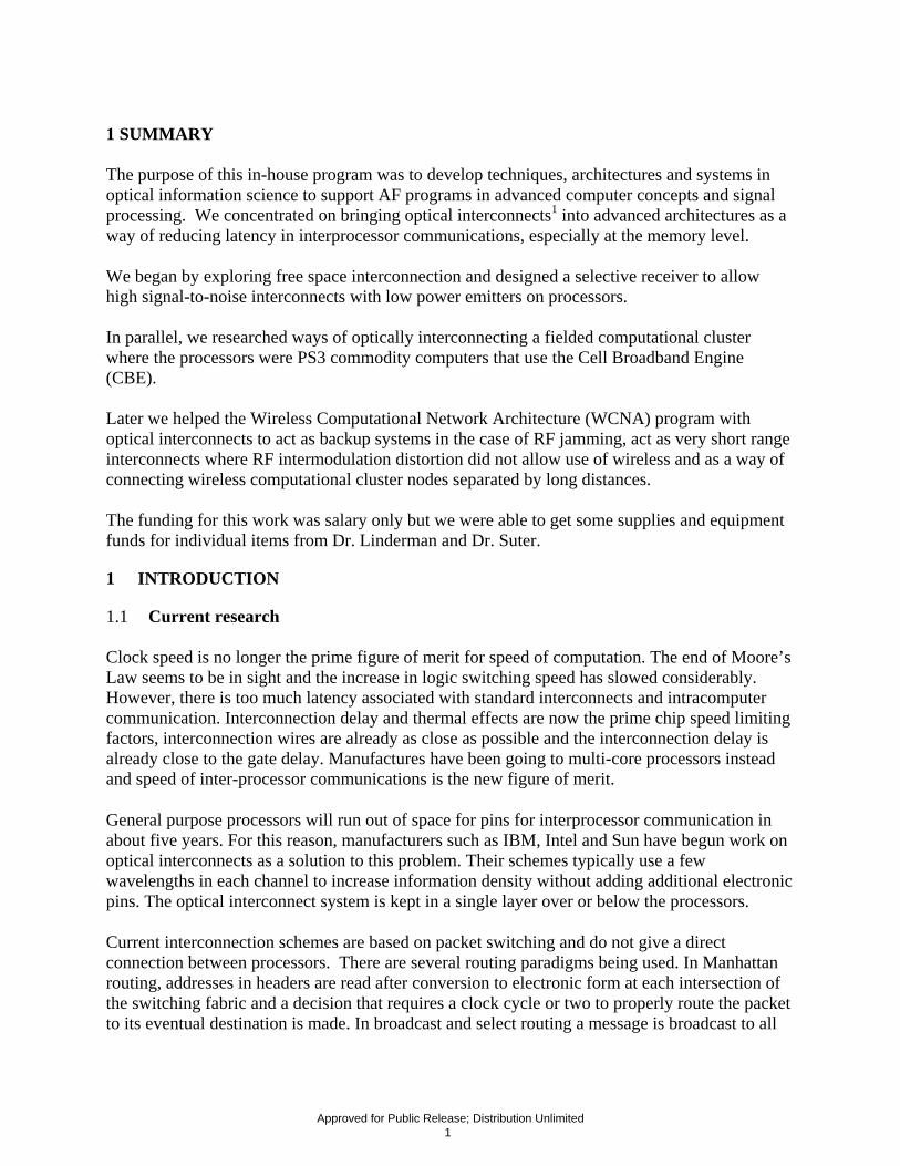
15.2.1 Simple Link Testing We concentrated on proving the concept of using commercially available hardware to create a direct optical link for inter-cluster communication, and, as previously mentioned, a potential backup communication method for the wireless inter-node communication system. The system was created using two Omnitron Systems Technology, Inc. FlexPoint GX/T UTP to fiber media converters along with four Thorlabs, Inc. F810APC-1550 collimators. The media converters are traditionally used by connecting their UTP port to the 100BASE-TX port on each computer. Two fibers were used, each for simplex communication between the two media converters. This configuration allowed for a significant increase in communication distance when compared to CAT5 cable. As seen in Figures 10 and 11, the intended setup/usage was modified to allow for the creation of a free space optical link. The computers were connected to the media converters using CAT5 cable; however, one of the cables needs to be a crossover network cable.
Figure 10. Regular Use Of Media Converters
Approved for Public Release; Distribution Unlimited 16
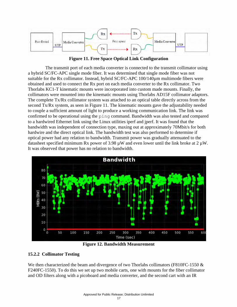
Figure 11. Free Space Optical Link Configuration
The transmit port of each media converter is connected to the transmit collimator using a hybrid SC/FC-APC single mode fiber. It was determined that single mode fiber was not suitable for the Rx collimator. Instead, hybrid SC/FC-APC 100/140µm multimode fibers were obtained and used to connect the Rx port on each media converter to the Rx collimator. Two Thorlabs KC1-T kinematic mounts were incorporated into custom made mounts. Finally, the collimators were mounted into the kinematic mounts using Thorlabs AD15F collimator adaptors. The complete Tx/Rx collimator system was attached to an optical table directly across from the second Tx/Rx system, as seen in Figure 11. The kinematic mounts gave the adjustability needed to couple a sufficient amount of light to produce a working communication link. The link was confirmed to be operational using the ping command. Bandwidth was also tested and compared to a hardwired Ethernet link using the Linux utilities iperf and jperf. It was found that the bandwidth was independent of connection type, maxing out at approximately 70Mbit/s for both hardwire and the direct optical link. The bandwidth test was also performed to determine if optical power had any relation to bandwidth. Transmit power was gradually attenuated to the datasheet specified minimum Rx power of 3.98 µW and even lower until the link broke at 2 µW. It was observed that power has no relation to bandwidth.
Figure 12. Bandwidth Measurement
15.2.2 Collimator Testing We then characterized the beam and divergence of two Thorlabs collimators (F810FC-1550 & F240FC-1550). To do this we set up two mobile carts, one with mounts for the fiber collimator and OD filters along with a picoboard and media converter, and the second cart with an IR
Approved for Public Release; Distribution Unlimited 17
camera, OD filters, and a Spiricon laser beam profiler. We used data from the Spiricon profiler to calculate the divergence of each collimator.
Figure 13. Media Converter & Collimator; Camera & Laser Beam Analyzer
15.2.3 Free Space Optical Propagation Range A MATLAB program was created to simulate free space optical propagation of the Tx beam to the Rx collimator to determine the maximum transmission distance. In a perfect world, with no atmospheric loss, the maximum distance was calculated to be approximately 3.5 km. The program takes wavelength, input power, output power required, Tx & Rx collimator sizes, and interface and atmospheric losses as inputs and calculates the maximum distance the beam can travel while accounting for divergence and losses, and at the same time meet the minimum power requirements of the Rx detector. It used the following equations
(1) Beam radius at distance z
(2) Beam intensity as a function of radius r at distance z
(3) Substitute equation 1 into equation 2
(4) Power as a function of distance z of a beam
with radius r Three outputs are provided, the maximum transmission distance is stored in a variable ‘maximum distance’, and two 3D surface plots are created showing the Tx & Rx Gaussian Intensity distributions. The light is modeled as a Gaussian beam and with the input parameters Transmitter Power of 1.75 mW; Minimum Receiver Power of 2.0 µW and a Divergence of 0.016º, it gives an ideal Maximum Distance of 3,600 m (~2.25 mi).
Approved for Public Release; Distribution Unlimited 18

15.2.4 Node to Node testing We then designed and had the machine shop construct two portable nodes for long range node-to-node optical communication testing. The setup is shown in Figure 14. The five computers of each node are connected to two Ethernet switches, as is the media converter. Additionally, an IEEE802.11g USB wireless adaptor card and external antenna is connected to the head-computer in each node. This setup, along with the externally mounted collimator mount demonstrated two optically connected nodes.
Figure 14. Two Node Setup
We will need to make arrangements to use one of the RRS test sites for further longer range testing.
16 CONCLUSIONS The main outcome of this research has shown that it is possible to use commercially available hardware to create a free space optical link. This link can provide high speed, wireless, unjammable communication over substantial distances. This is a crucial component of a successful battlefield cluster system, and the fact that it was shown to be feasible is a huge success. There are several possibilities to further improve this system in the future. First, if the computers ever utilize 1GigE Ethernet ports, the bandwidth of the link would increase 10x from 100 Mbit/s to a theoretical maximum of 1Gb/s. This is almost twice the bandwidth attainable from
Approved for Public Release; Distribution Unlimited 19

IEEE802.11n utilizing four channels, 600 Mbit/s, and almost 7x the bandwidth of one channel. Another option is possible by switching from the EPIA PX-10000G to the Compal MID picoboard. The MID has wireless Ethernet and GPS built in, and USB ports which could be used with an USB to Ethernet adaptor to interface with the media converter. The exciting possibility with this device is using the built in GPS to assist with pointing and tracking of the optical communication beams. Another idea utilizing the MID is to create a hybrid node of four PX-10000G computers and one MID. This would utilize the increased computing power of the PX-10000G, but at the same time, incorporate the GPS and wireless Ethernet of the MID into each node. However, if wireless and GPS are desired, there are other options as well. The Planex GW-USMicroN wireless adaptor21 and USGlobalSat’s ND-100 USB GPS receiver22 can be connected to the PX-10000G to give it the same functionality as the MID. A potential system using this configuration can be seen in Figures 15 and 16.
Figure 15. Cluster to Cluster Communications
Approved for Public Release; Distribution Unlimited 20

Figure 16. Future System
The end goal is to create the fastest, lightest system possible for potential application in an environment such as a UAV or other mobile battlefield systems. These systems may be constructed of several nodes communicating in close proximity (a cluster) which may need to pass information over a relatively large distance to another cluster constructed of several nodes, as seen in Figure 15. The long range option is based on building-to-building high speed optical communication (up to 1.5 Gbps @ 2-3 km). The idea is that there would be groups of picoboards in one area that require information from another group of picoboards in an area that is out of RF wireless or the medium range option’s maximum distance. Commercial units like the SkyFiber link in Figure 16 can take RF wireless signals or wired signals from the picoboards in the local area collected by a RF wireless antenna (data rate of 54 Mbps), send them through an
Approved for Public Release; Distribution Unlimited 21
IP addressable router and convert them to an optical signal and transmit; both sides of the system are true transceivers. The whole system is 802.11g compatible. This option is more expensive but may only be needed for specific applications.
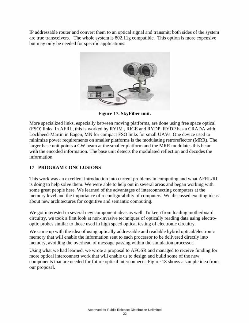
Figure 17. SkyFiber unit.
More specialized links, especially between moving platforms, are done using free space optical (FSO) links. In AFRL, this is worked by RYJM , RIGE and RYDP. RYDP has a CRADA with Lockheed-Martin in Eagen, MN for compact FSO links for small UAVs. One device used to minimize power requirements on smaller platforms is the modulating retroreflector (MRR). The larger base unit points a CW beam at the smaller platform and the MRR modulates this beam with the encoded information. The base unit detects the modulated reflection and decodes the information.
17 PROGRAM CONCLUSIONS This work was an excellent introduction into current problems in computing and what AFRL/RI is doing to help solve them. We were able to help out in several areas and began working with some great people here. We learned of the advantages of interconnecting computers at the memory level and the importance of reconfigurability of computers. We discussed exciting ideas about new architectures for cognitive and semantic computing. We got interested in several new component ideas as well. To keep from loading motherboard circuitry, we took a first look at non-invasive techniques of optically reading data using electro-optic probes similar to those used in high speed optical testing of electronic circuitry. We came up with the idea of using optically addressable and readable hybrid optical/electronic memory that will enable the information sent to each processor to be delivered directly into memory, avoiding the overhead of message passing within the simulation processor. Using what we had learned, we wrote a proposal to AFOSR and managed to receive funding for more optical interconnect work that will enable us to design and build some of the new components that are needed for future optical interconnects. Figure 18 shows a sample idea from our proposal.
Approved for Public Release; Distribution Unlimited 22

Figure 18. Low Impact Plasmonic EO Conversion
Approved for Public Release; Distribution Unlimited 23

19 REFERENCES
1. Petar Pepeljugoski, et al., “Data Center and High Performance Computing Interconnects for 100 Gb/s and Beyond”, Optical Fiber Communication and the National Fiber Optic Engineers Conference, pp. 1-3, 2007; Drew Alduino, et al.,” Integration Challenges for Optical Interconnects”, Photonics Packaging, Integration, and Interconnects VIII, Alexei L. Glebov, Ray T. Chen., eds., Proc. of SPIE Vol. 6899, 689910, (2008).
2. Richard M. Fujimoto, Parallel Discrete Event Simulation, Communications of the ACM, Vol. 33 No. 10, pp. 30-53, October 1990
3. Susumu Shibusawa, et al., ‘Scatter and Gather Operations on an Asynchronous Communication Model, ‘SAC ’00, March 19-21, Como, Italy
4. Srinivas Devadas , “Cache Coherence”, (http://people.csail.mit.edu/devadas/6.004/Lectures/lect23/).
5. Harris Turk, “Photonic Integration and Information Assurance”, AGED/DSB Special Technology Area Review on Photonic Integation, Session 1 Talk, 2007.
6. Nael Abu-Ghazaleh, “Optimization of the SPEEDES Parallel Discrete Event Simulation Engine on a Heterogeneous HPC Cluster”, AFRL Summer Report 2004.
7. Alfredo Buttari, et al., “A Rough Guide to Scientific Computing On the PlayStation 3”, Technical Report UT-CS-07-595 Version 1.0 by Innovative Computing Laboratory, University of Tennessee Knoxville, May 11, 2007 8. http://pc.watch.impress.co.jp/docs/2006/1111/ps3.htm
9. Liu Lanjun (Univ. of Sci. & Technol. Beijing, Beijing, China); Zhang Xiaotong; Wang, Jingcun “Design of optical interconnection network adapter based on DDR DIMM bus for cluster system”, Computer Engineering, v 33, n 14, 20 July 2007, 207-9 Language: Chinese
10. Tadao Nagatsuma and Mashahiro Tsuchiya, "Optical Measurement Technologies for High Frequency Electronics", Ch. 4 of Microwave Photonics, Chi H. Lee, ed., CRTC Press, 2007.
11. http://www.hdmi.org/learningcenter/faq.aspx#94
12. USB-520 USB Optical Fiber Extender (http://www.opticomm.com/USB-520___151)
13. USB-520 USB Optical Fiber Extender (http://www.opticomm.com/USB-520___151)
14. Avinash Karanth Kodi and Ahmed Louri, “System simulation methodology of optical interconnects for high performance computing systems”, J. Opt. Networking, Vol. 6, No. 12, December 2007.
15. Ben Wun, "Survey of Software Monitoring and Profiling Tools" (http://www.cs.wustl.edu/~jain/cse567-06/ftp/sw_monitors2.pdf)
16. Mack W. Riley and Mike Genden, "Cell Broadband Engine Debugging for Unknown Events", IEEE Design & Test of Computers, September–October 2007; Dac C. Pham et al., "Overview of the Architecture, Circuit Design, and Physical Implementation of a First-
Approved for Public Release; Distribution Unlimited 24

Generation Cell Processor", IEEE JOURNAL OF SOLID-STATE CIRCUITS, VOL. 41, NO. 1, JANUARY 2006, p. 179
17. "Electro-optic sampling", in Encyclopedia of Laser Physics and Technology (http://www.rp-photonics.com/electro_optic_sampling.html
18. Joseph Chaiken, Ethan Voss, Joseph M. Osman, Rebecca Bussjager, “Enabling photonic technologies based on electrochromic and photochromic tungsten oxide”, Proceedings of the SPIE, Vol. 4386, pp. 53-61, April 2001.
19. http://www.via.com.tw/en/products/embedded/ProductDetail.jsp?id=472
20. http://www.omnitron-systems.com/products/4700_gxt_flexpoint.php
21. http://www.planex.net/product/wireless/gw-usmicron.htm
22. http://www.usglobalsat.com/p-590-nd-100.aspx
Approved for Public Release; Distribution Unlimited 25

20 APPENDIX A
Approved for Public Release; Distribution Unlimited 26
A MIMO-INSPIRED RAPIDLY SWITCHABLE PHOTONICINTERCONNECT ARCHITECTuRE
Henry Zmuda University of Florida
Department of Electrical and Computer Engineering Gainesville, FL
Joseph Osman, Michael Fanto and Thomas McEwen Air Force Research Laboratory, Information Directorate
Rome, NY
ABSTRACT
It is well-known that interconnect issues pose a significant bottleneck with regard to im roving the perfonnance of high-speed integrated systems such as a cluster of computer processing units. P wer, speed (bandwidth), and size all affect the computational perfonnance and capabilities of future sys ems. Highspeed optical processing has been looked to as a means for eliminating this interconnect bottleneck. Presented here are the results of a study for a novel optical (integrated photonic) processor hich would allow for a high-speed, secure means for arbitrarily addressing a multiprocessor system. Thi paper will present analysis, simulation, and optimization results for the architecture as well as conside tions for a proof-of-concept level system design. The architecture takes advantage of spatial and wavelen diversity and in this regard may be regarded as a Multiple Input Multiple Output (MIMO) architeCture.
i
A given node to be addressed, rather than having a wired metal contact as an output, basi as a ra iating laser source that has been modulated with the data to be conveyed to another point in the system. E h processor node radiates a diff~rent optical wavelength. Each individual wavelength is chose11, for xample, to correspond to the wavelengths associated with a WDM ITU grid. All wavelengthsl are in ident on a coherent fiber bundle which acts as an array receiver. Unlike conventional phased arrays, the receive elements are spaced many wavelengths apart giving rise to a large number of grating lobe . It will be shown that by using appropriate photonic/optical signal processing methods any node of e processor cluster can be randomly and rapidly addressed using high-speed phase shifters ( electrooptic r others) as control elements. The diversity techniques employed achieve high gain and a narroW beam idth in the direction of the desired node and high attenuation with regard to the signals from all: other odes. As is often the case of MIMO-bases systems, overall perfonnance exceeds that of diffraction li ited array processing.
In addition to the interconnect application discussed, the methods described in this paper applied to other applications where rapid electrical (non-mechanical) optical beamsteering is as raster scanned laser radar systems and tracking, guidance, and navigation systems.
KEYWORDS: Free-space optical interconnects, Optical Phased Arrays, High-Speed Optical Beamsteering, Optical MIMO, Microwave Photonics
1 INTRODUCTION
1.1 Optical Phased Arrays
The ability of phased array antennas for beam steering application are well known, and syste have searched for ways to transition these benefits to optically-based systems [1~3]. T similarities exist between optical and RF /microwave beamfonning systems there exist
designers ugh many significant
Enabling Photonics Technologies for Defense, Security, and Aerospace Applications V, edited by Michael J. Hayduk, Peter J. Delfyett Jr., Andrew R. Pirich, Eric J. Donkor, Proc. of SPIE Vol. 7339,
73390K · © 2009 SPIE ·CCC code: 0277-786X/09/$18 · doi: 10.1117/12.822116
Proc. of SPIE Vol. 7339 73390K-1

Approved for Public Release; Distribution Unlimited 27
differences well. RF phased array antennas can provide, in theory, a diffraction limited beam on-target with a 3-d beamwidth on the order of )JNd, where A is the RF carrier center wavelength, d is the array element sp ing, and N is the number of radiating elements. Through coherent addition of fields, the power on-target is roportional to lfpo where Po is the power radiated by each element. Further, and perhaps most significantl , the antenna pattern for a phased array antenna can be steered (scanned) electronically as well as shaped, hich, for the case of a narrow RF bandwidth, is accomplished simply by means of phase and amplitude c ntrol of the carrier signal at each radiating element. Electronic scanning of the beam allows for a rapidly r configurable far-field beampattern without physical motion of the antenna. These last two features, n ely the directional gain and non-mechanical beam pointing, are obviously attractive for optical beam steeri g systems as well.
These bene 1ts of RF array beamfonning techniques are mitigated however when one considers the practical li itations imposed by a phased array system operating at an optical carrier. Since the individual lasers are g nerally not coherent, the power for N lasers increases by a factor N as compared to If for coherent r iators. More significantly, the lack of coherence among the laser sources prevents the use of array beam onning methods in the fullest sense. Consequently non-electronic steering of the beam, mechanical or otherwise, is still required. Even with an array of coherent (phase-locked) laser sources, coherent b forming is still poses problems. This is because conventional beamforming techniques require that he inter-element array spacing be at most equal to one-half the operational wavelength or d .:::_ ')..)2. For p tical systems with an operating wavelength on the order of 1 -- 2 microns, such spacing is impossible. ndeed, the core diameter alone of a single-mode optical tiber is on the order of several microns and several tens of microns for a multi-mode fiber. Array element spacing on the order of many wavelength results in the production grating lobes, where energy is radiated in many directions and gives rise to spati ambiguity.
These cons derations unfortunately have made conventional array beamforming techniques effectively impractical or optical applications. The sought after array advantage of increased power and electronic steering cap ility applied to optical systems requires a new paradigm which is introduced in the section to follow.
This paper amines the use of MIMO techniques to achieve optical beamsteering. MIMO radar techniques have been otivated by recent advances in communication theory. It has been shown that unlike a convention phased array which transmits appropriately weighted, delayed (or phase-shifted) versions of the same si nal, a MIMO array transmits multiple signals that are, in general, quite different from each other. This ifference, termed waveform diversity, fonns the essence ofMIMO arrays, and enables superior capabilities compared with standard phased-array radar technology (4-8]. For example, for either colocated or b -static transmit and receive antennas, MIMO radar has been shown to offer higher resolution (4] and sen itivity (to detecting slowly moving targets) (5], better parameter identifiably (6], and direct appiicabili of adaptive array techniques [7, 8]. In the field of communications MIMO approaches have been shown to improve the bit error rate in a communications channel beyond that of the Nyquist limit. Here too wi 1 the techniques presented allow for beam resolution which far exceeds the diffraction limit of the N-cleme t aperture.
2 THEORY OF OPERATION
2.1 Genera MIMO Array Topology
Figure I ill !rates the MIMO concept in conceptual form. TheM radiating sources transmit independent signals X0,- ·,xM-I. These signals are detected by N receive elements y 0,- · ·,yN-I. Note that a particular
receive ele ent, say Yn, receives Mweighted independent signalsan,oX0 , • • • ,an.M-txM _1, where the
coefficients am.n account for the propagation effects from transmit element m to receive element n.
Proc. of SPIE Vol. 7339 73390K-2

Approved for Public Release; Distribution Unlimited 28
Yo Y1 Y.v-1
LJ ... 1 11ko u=l ,FN-1
~ R
• m=M-11
XM-1
•'igure 1: Conceptual illustration of a MIMO-bases array architecture. Assumed here is a Uniform inear Array (liLA) Topological architecture for an M-element-transmit and N·element-receive MIMO array wit the receiver assumed to be in the far-field of the transmitter.
Consider the case of a uniform linear array (ULA) for both the transmitter and receiver, as sho in Figure 1. The radiating elements are spaced by a distance dr while the receiver elements are spaced by dR. It is assumed that both d, and dR are much greater than the usual half-wavelength spacing. Examinat on of Figure I shows, that with the usual far-field approximations, a signal (electric or magnetic field xm (t) emanating from the rrfl! radiator and upon reception at the rfh receiver element will be of the fo
Ym.n (t) = am.nxm (t- Tm.n) (I)
-1 In (1 ), am,n is an attenuation factor which accounts for the loss due to the scattering cross-secti n, the r propagation loss, as wei! as other losses such as absorption and scattering from other obstacles i the propagation path. The time delay term Tm,n is found from geometrical considerations and is give by,
Tm,n = n" (R+nd11 sinO" -md, sinO.,), m = 0, I, ... , M -I, n = 0, I, ... , N -I (2) c
where no is the refractive index of the intervening medium, here assumed constant and equal to nity, c is
the speed of light in air, and d, and d Rare the element spacing for the transmit and receive arr ys,
respectively. The distances from the m = 0 element of the transmitter array to the n = 0 eleme t of the receive array is designated as R . It is assumed that the receiver and transmitting arrays are in th other's far-field for and that R a makes an angle B., with respect to the normal of the transmit array an receive
arrays as shown.
Examination of Figure I and Equation (I) shows that the signal xm ( t), m = 0, ... , M -I , 'ves at
each receiver element location as y n ( t), m = 0, ... , M -l , with a unique time delay specifi d by
Equation (2). This in tum suggests that there are possibly M · N unique conditions that may b used to accurately estimate the position of the array. It is such a multiplicative effect that we wish to ex loit in this system.
2.2 Multi-Wavelength Diversity Beamsteering
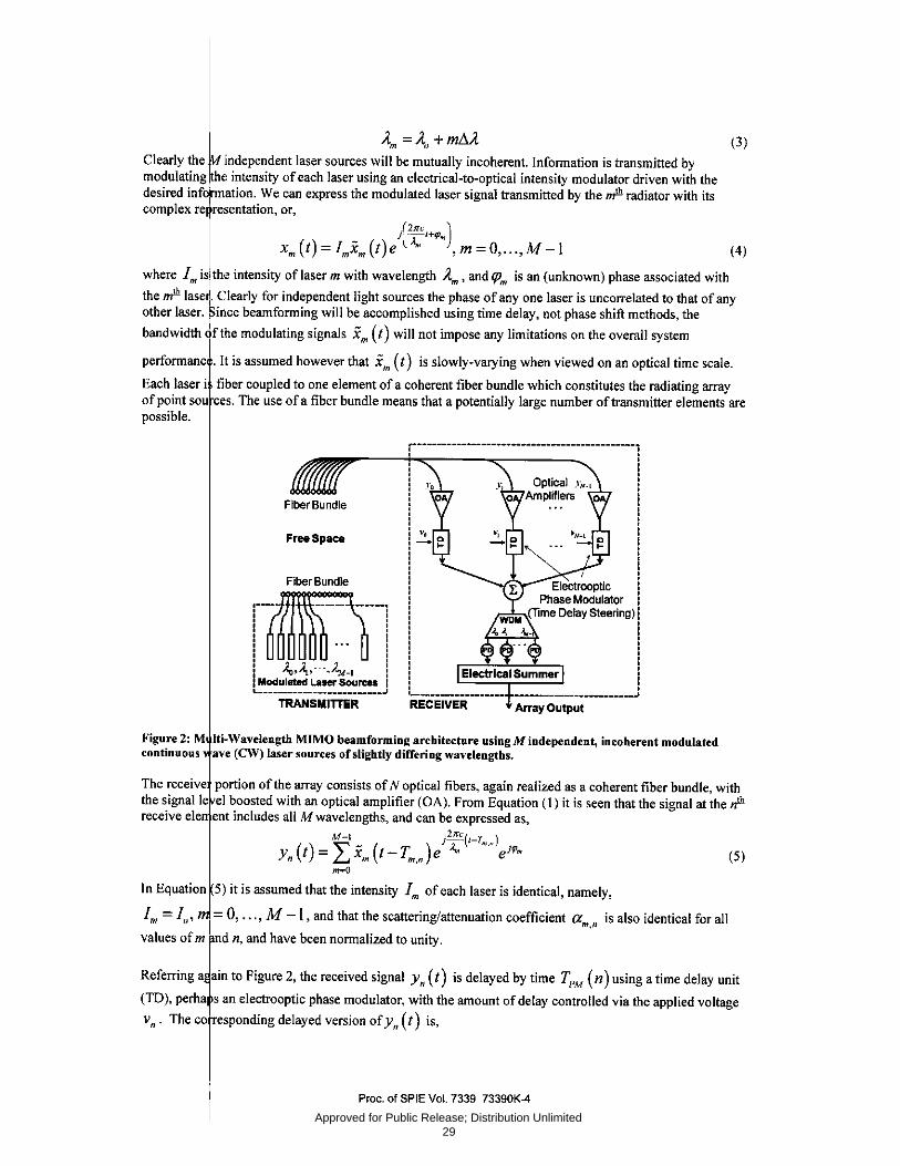
The architecture of the MIMO-based optical transmit-receive employing wavelength diversity i shown in Figure 2. The transmitter portion of the system consists of M independent CW lasers, each ope ting a slightly different wavelength ll.m, where
Proc. of SPIE Vol. 7339 73390K-3
Approved for Public Release; Distribution Unlimited 29
Clearly the modulating desired info complex re
Am =A,, +mAA independent laser sources will be mutually incoherent. Information is transmitted by e intensity of each laser using an electrical-to-optical intensity modulator driven with the ation. We can express the modulated laser signal transmitted by the m1h radiator with its
resentation, or,
(3)
(4)
where lm is the intensity of laser m with wavelength A..m, and qJm is an (unknown) phase associated with them"' lase . Clearly for independent light sources the phase of any one laser is uncorrelated to that of any other laser. ince beamforrning will be accomplished using time delay, not phase shift methods, the bandwidth fthe modulating signals xm (t) will not impose any limitations on the overall system
perforrnanc . It is assumed however that xm ( t) is slowly-varying when viewed on an optical time scale.
Each laser i fiber coupled to one element of a coherent fiber bundle which constitutes the radiating array of point sou ces. The use of a fiber bundle means that a potentially large number of transmitter elements are possible.
Free Space
Fiber Bundle
r-~------------~ ' ' I I I ••• I
' ' ' ' , • • ). I : Ao.A,..·. ·• "M-1 : ! Modulated Laser Sources 1 1..---------------------.J
TRANSMITTER Array Output
Figure 2: M lti-Wavelength MIMO beamforming architecture using M independent, incoherent modulated continuous ave (CW) laser sources of slightly differing wavelengths.
The receive portion of the array consists of N optical fibers, again realized as a coherent fiber bundle, with the signalle el boosted with an optical amplifier (OA). From Equation (I) it is seen that the signal at the tfh receive ele ent includes all M wavelengths, and can be expressed as,
M-1 _llrC:.(t-T )
Y,(t)= ,Ixm(t-Tm,n)/ A,. "" ej•.. (5) m=O
In Equation 5) it is assumed that the intensity /m of each laser is identical, namely,
lm = 1,,, m = 0, ... , M -I , and that the scattering/attenuation coefficient a is also identical for all m.n values of m nd n, and have been normalized to unity.
Referring a ain to Figure 2, the received signal y n ( t) is delayed by time ~'M ( n) using a time delay unit
(TD), perha san electrooptic phase modulator, with the amount of delay controlled via the applied voltage V n • The co esponding delayed version of y n ( t) is,
Proc. of SPIE Vol. 7339 73390K-4

Approved for Public Release; Distribution Unlimited 30
M-1 /Hc(t-1;,,,.-1pu(n)) Y, [t- Tf>M (n) J = L xm (t- Tm.n- TPM (n) )e ... e1•· (6)
m=O
An important consideration for this architecture concerns the ability of a commercial electroopt c phase modulator to provide the necessary amount oftime delay needed to electronically steer the arra aperture. To address this concern, consider that an N-element unifonn linear array with element spacing would
nd require a maximum time delay of±( N -l )-"- to steer the aperture by±90°. But since the Iemen!
c spacing here is small (typically a hundred wavelengths, with the wavelengths on the order of a icron), a simple calculation shows that the maximum time delay required is on the order of hundreds of femtoseconds. Time delay on this order is obtainable, in principle, from a commercially availab e device such as a Lithium Niobate electrooptic phase shifter.
Since the modulating signal Xm ( t) is narrowband when compared with its optical carrier, and ince
~'M ( n) « Tm.n = n, R, the argument in Equation (6) is well-approximated by c
Xm (t- Tm.n- ~'M (n)) = Xm (t- ~ (Rn + Rr)) = Xm
and so Equation (6) may be written,
~ /Hc(t-Tr(m)-1R(n)-1j,At(n)) Yn(t-~,M(n))= L,xme '- e1
•· m:O
(7)
(8)
As shown in Figure 3 the delayed signals Yn (t- ~'M) are summed (optically) using an equal ath-length
summer such as a I x N coupler. Though not shown explicitly in Figure 3, each of the fibers (w veguides) at the summer inputs must have a means of equalizing the path length. For example. this can be accomplished using a variable retro-reflecting prism for a coarse delay adjustment and an addif nal electrooptic phase modulator for fine adjustment. These delays are used solely for path-length e ualization and are not used for beam steering. Ideally these delays, once set, would require further ad jus ent to only compensate for any long-term drift. Making use of Equation (2) the output of the summer can b written as,
Ys (t) = I:'IxmeJ';:_'(t-1~.(m)-1; . ..,(n))eJ•. = IxmefDt-7(R-mdr•in8,)JeJ•. I;e-Jn,~(n sin6'0 +Tn,(n))
n~ m~ m:::O n=O
(9)
Equation (9) suggests that we choose TI'M ( n) = -n n,dR sine, where e represents the desi d steer
angle. Noting that the second sum on the right-hand-side of (9) can be expressed in closed form Equation (9) becomes,
(10)
where
N-l2nn . . sin(N"n"d,(sinl'l,-sini'I)J -j-=dl!(sm80 -sm8) A,
em ( 61, 8,,) = e 2
ol,. -----'7( ___!!!_m ----)<!-sin ::o dR(sinB,, -sin B)
(11)
Equation (II) clearly reveals that the beam characteristics are a function of wavelength Am, a c aracteristic
that will be used to great advantage in the analysis that follows. The output of the summing dev ce is then
Proc. of SPIE Vol. 7339 73390K-5

Approved for Public Release; Distribution Unlimited 31
directed to wavelength demultiplexer (WDM in Figure 3 ), realized, for example, using an arrayed waveguide rating device, which separates the individual wavelength components of the summed signal. The output fthe nth WDM (corresponding to Am ) is,
/Jrc(t~-(R-mdrsin80 )) .
YwnM. (t)=xmcm(B,B,,)e -'m ' eN• (12)
where an id al, unit amplitude rectangular bandpass transmission characteristic for the WDM has been assumed.
Each of the wnM. ( t ), m = 0, , , M -1 signals are now detected using Mhigh-speed photodiodes, and these detect d electrical signals can be written as
YwoM. (t) = Xm lcm ( B,B,)I ( 13)
The electric I detection process strips off any optical phase. This eliminates the random phase term associated ith each laser as well as any phase associated with the propagation delay from the transmitter to the receiv element. This in tum shows that the WDM output is not a function of the transmitter aray spacing. Eq ation (13) also shows that the nth WDM output consists ofthe m111 modulating signal xm weighted by the angular dependent factor I em ( B, B, Jl· This weighting function I em ( B, B,, Jl is simply the
array factor fan N-element uniform linear array with element spacingd R. A careful examination of Equation (9 reveals two important features of the multi-wavelength approach; the first is that the main lobe occurs whe (} = (}
0 for all wavelengths Am as expected for a time-steered array. The second feature is that
A sincedu » m, many grating lobes will be present, but unlike the main lobe, the angular location of the
2 grating lobe varies with wavelength. Specifically, grating lobes occur when
sin ( ~:· R (sin B" -sin Be;))= 0 or when '7," d, (sin B,- sin Be;)= p;r where pis an integer.
Solving for e position Be; of the grating we find,
Be; = arcsin (sin B, - p _3,__), nodR
(14)
where l A J is the largest integer less than _3,_ . This property of an array factor, namely that main no R nodR
beam that is fixed in location while grating lobes (and null locations) vary with wavelength has been previously u ed to implement a broadband RF beamforming system with steerable broadband nulls [10, II]. As will subsequently shown, this diversity in the location of the grating lobes/null positions as a function oft e wavelength is what allows for the design of a high-resolution electronically scanned array.
Referring ag in to Figure (2), each detected WDM output is now summed using an equal path length electrical su mer. This gives the final array output as,
M-1 M-l M-l
y(t)= LYwnM. (t)= LXmlcm(B,B,,)I:<O:xm,mnLicm(B,B,)I (15) m="l m=l m=l
Where xm,m• is the maximum amplitude ofxm. Further note that the sum in (15) will add maximally only
for B = B". his is easily seen by examination of Figure (3), which illustrates the magnitude of em (B) form= 0, .. , 9, as a function of the parameter (angle)(}. For clarity Figure 3 shows a 1'zoomed-in" portion ofth angular spectrum that includes the main beam along with the first grating lobe. It is seen how
Proc. of SPIE Vol. 7339 73390K-6
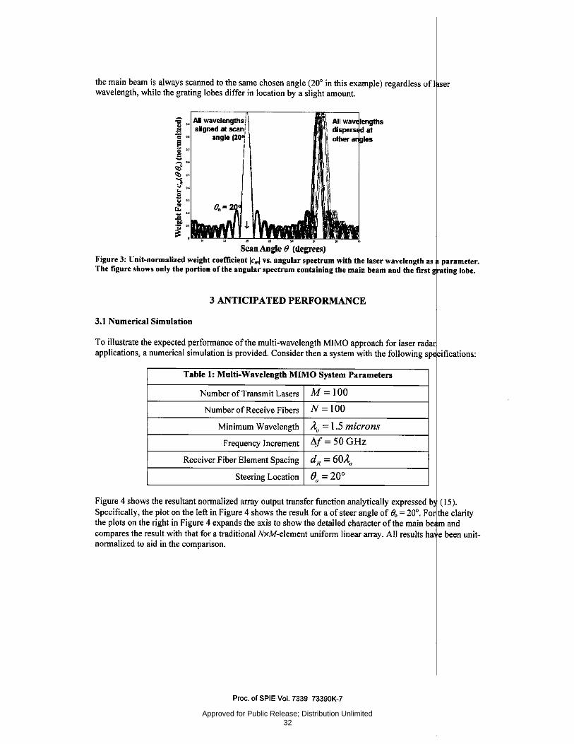
Approved for Public Release; Distribution Unlimited 32
the main beam is always scanned to the same chosen angle (20' in this example) regardless ofl er wavelength, while the grating lobes differ in location by a slight amount.
Scan Angle 8 (degrees) Fi~!:ure 3: Unit~normalized weight coefficient lcml vs. angular spectrum with the laser wavelength as parameter. The figure shows only the portion of the angular spectrum containing the main beam and the first ating lobe.
3 ANTICIPATED PERFORMANCE
3.1 Numerical Simulation
To illustrate the expected performance of the multi-wavelength MlMO approach for laser radar applications, a numerical simulation is provided. Consider then a system with the following sp ifications:
Table 1: Multi-Wavelength MIMO System Parameters
Number of Transmit Lasers M=100
Number of Receive Fibers N=100
Minimum Wavelength A, = 1.5 microns
Frequency Increment l'lf=50GHz
Receiver Fiber Element Spacing dR = 60.4,,
Steering Location B =20° '
Figure 4 shows the resultant normalized array output transfer function analytically expressed b (15). Specifically, the plot on the left in Figure 4 shows the result for a of steer angle of 8, ~ 20'. Fo the clarity the plots on the right in Figure 4 expands the axis to show the detailed character of the main be and compares the result with that for a traditional NxM-element uniform linear array. All results ha e been unitnormalized to aid in the comparison.
Proc. of SPIE Vol. 7339 73390K-7

Approved for Public Release; Distribution Unlimited 33
,., • ,, ro
" , .. .. .. '" ,. .-"" "' 104 element ULA
m "' j
~· ,.
~· ~· r ..
Figure 4: Si ulated response for an ten-element transmit, ten-element receive MIMO laser radar. The plot on he left shows the effective radiation pattern steered to an angle of 20'. The plot on the top right sh ws the sibelobe lenes while the plot on the lower right compares the beamwidth for the 20' MIMO rray pattern with that of a IOOxiOO-element Uniform Linear Array (ULA).
4 CONCLUSIONS 4.1 Summa
The analysis presented and illustrated by simulation shows that even for arrays with element spacing greater that t e usual half-wavelength, significant advantages are realized. First, as expected, the directional gain on-targ is increased by a factor of M · N while using only M lasers. Secondly it is seen that the beamwidth t at of a M · N - element array. For a receiver element spacing exceeding 40~1 , which, under normal circu stances would produce many grating lobes, produces only one main beam. The diversity approach uti ized here, namely the use multiple laser wavelengths, results in a significant amplitude reduction at II angles except that of the main lobe. Tradeoffs among the various system parameters would produce ad ign that has been optimized for a particular interconnect application.
S REFERENCES
[1] H. Zmud and E.N. Toughlian. Photonic Aspects of Modem Radar. Boston, Artech House, 1994.
[2] P.F. Me anamon, T.A. Dorschner, D.L. Corkum, L.J. Friedman, D.S. Hobbs, M. Holz, S. Liberman, H.Q. Nguye , D.P. Resler, R.C. Sharp, and E.A. Watson. "Optical Phased Array Technology," Proceedings Of The IEEE, Vol. 84. No.2, February 1996, pp. 268-298.
[3] N.A. Riz , Editor, Selected Papers on Photonic Control Systems for Phased Array Antennas, SPlE MilestoneS ries Volume MS 136. Bellingham, Washington: SPIE Optical Engineering Press, 1997
[4]1. Bekke an and J. Tabrikian. "Spatially coded signal model for active arrays," The 2004 IEEE Intern tiona! Conference on Acoustics, Speech, and Signal Processing, Montreal, Quebec, Canada, val. 2, pp. ii 09-ii/212, March 2004.
[5] J. Li and . Stoica, "MIMO radar- diversity means superiority," The Fourteenth Annual Workshop o Adaptive Sensor Array Processing, MIT Lincoln Laboratory, Lexington, MA, June 2006.
[6] L. Xu, J Li, and P. Stoica, "Adaptive techniques for MIMO radar,'" 4th IEEE Workshop on Sensor Arr and Multi-channel Processing, Waltham, MA. July 2006.
[7] L. Xu, J Li, and P. Stoica. "Radar imaging via adaptive MlMO techniques,'" 14th European Signal Proc sing Colfference, (invited), Florence, Italy, September 2006. (available on the website: : /www.sal.ufl.edu/xuluzhou!EUS1PC02006. df).
Proc. of SPIE Vol. 7339 73390K-8

Approved for Public Release; Distribution Unlimited 34
(8] P. Stoica, J. Li, andY. Xie, "On probing signal design for MIMO radar," to appear in lEE Transactions on Signal Processing.
[9] N. Levenon, "Noncoherent Pulse Compression",/£1!.."'£ Transactions on Aerospace and El ctronic Systems, Vol. 42, No.2, April2006, pp. 756-765.
(!OJ H. Zmuda, E.N. Toughlian, M.A. Jones, P.M. Payson, "Photonic Architecture for Broadb nd Adaptive Nulling with Linear and Conformal Phased Array Antennas", Fiber and Integrated Optics, vol. 19, no. 2, March 2000, pp. 137- 154.
(11]11. Zmuda, E.N. Toughlian, P. Payson, and H. Klumpe, Ill, "A Photonic Implementation a Wideband Nulling System for Phased Arrays", IEEE Photonics Technology Letters, Vol. 10, . 5, pp. 725-727, May 1998.
Proc. of SPIE Vol. 7339 73390K-9