stephan haensel - lp subsystems meeting - desy silicon envelope for the large prototype tpc @ desy...
TRANSCRIPT
Stephan Haensel - LP Subsystems Meeting - DESY
Silicon Envelope for the Large Prototype TPC @ DESY
S. Haensel1, T. Bergauer1, M. Dragicevic1, M. Krammer1,T. Barvich2, A. Dierlamm2, F. Hartmann2, B. Ledermann2,
T. Müller2, H.J. Simonis2
1 Institut fuer Hochenergiephysik (HEPHY), Vienna, Austria2 Institut fuer Experimentelle Kernphysik (IEKP), Universitaet Karlsruhe, Germany
LP Subsystems Meeting – DESY25/26.02.2008
Stephan Haensel - LP Subsystems Meeting - DESY
Contents
• Introduction• Silicon Envelope• Cosmic Setup• Done & To Do
Stephan Haensel - LP Subsystems Meeting - DESY
Introduction
• The SiLC collaboration will participate at the Large Prototype TPC (LPTPC) at the EUDET facility at DESY II.
• SiLC will design, build and install position sensitive detector modules around the LPTPC made of silicon microstrip sensors that can be used as telescope.
• The design will allow an easily exchange of the modules to enable tests of different sensor- and chip- designs.
• This setup will also help to verify if a silicon envelope for a future linear collider TPC is reasonable.

Stephan Haensel - LP Subsystems Meeting - DESY
Top view of the Setup
(Drawing from: http://www-flc.desy.de/tpc/)
ID of magnet inner bore 850 mm measured minimum 846 mmSiLC detectors 2 x 35 mmclearance inside of SiLC 780 mm extra clearance 2 x 5 mmOD of field cage 770 mm field cage wall 2 x 25 mm ID of field cage 720 mm
radial dimensions:

Stephan Haensel - LP Subsystems Meeting - DESY
Silicon Envelope• four silicon modules will be installed:
- two in front and two behind the TPC, with respect to the e--beam two independent support structures are needed
- on each side: one horizontal module consisting of two daisy-chained sensors and one vertical module consisting of one sensor
• movable support system is needed because it must be possible to scan the TPC- the TPC and the magnet will move relative to the beam
TPC Magnet
Beam
Rails Module
- the sensors have to stay inside the beam line
sensors must be movable orthogonal to the beam and along a curved rail this movement must be coupled with the movement of the TPC and the magnet in addition the two sides have to move independently from each other

Stephan Haensel - LP Subsystems Meeting - DESY
Readout - Plan A -> SiLC Chip + Readout
Next Chip:-) 128 channels in 130nm CMOS-) Improved shaper (reduced noise)-> first test beam foreseen in Oct. 08 @ CERN
Current Chip:-) 4 channels in 130nm
CMOS-) functionality verified
in beam tests
(from: Thanh Hung Pham @ 6th SiLC meeting)
(from: A. Savoy-Navarro @ 6th SiLC meeting)

Stephan Haensel - LP Subsystems Meeting - DESY
Readout - Plan B -> Adopted CMS Readoutbased on APV25 readout chipcomponents: green: available
orange: to be designedred: still searching
forIf two working CCUMs can be found:
-) two ICBs will be designed-) it has to be verified that the system works with the needed cable lengths
(by Alexander Dirlamm)
Caption:
ICC…InterConnect Card
ICB…InterConnect Bus
AOH…Analog Optohybrid
CCUM…Central Control Unit Module
FED…Front End Driver
FEC…Front End Controller
Stephan Haensel - LP Subsystems Meeting - DESY
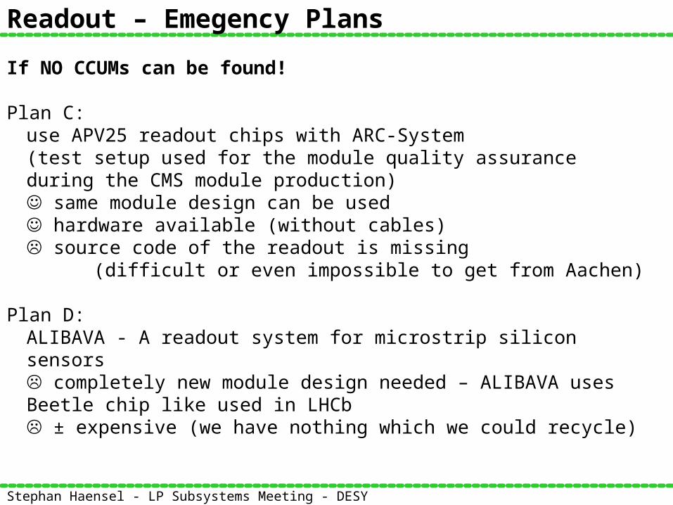
Readout – Emegency Plans
If NO CCUMs can be found!
Plan C:use APV25 readout chips with ARC-System(test setup used for the module quality assurance during the CMS module production) same module design can be used hardware available (without cables) source code of the readout is missing
(difficult or even impossible to get from Aachen)
Plan D:ALIBAVA - A readout system for microstrip silicon sensors completely new module design needed – ALIBAVA uses Beetle chip like used in LHCb ± expensive (we have nothing which we could recycle)

Stephan Haensel - LP Subsystems Meeting - DESY
2D LayoutMagnet
Beam
1 Sensor Module
2 Sensor Module
radial dimensions: magnet inner bore 425 mm measured minimum 423 mmSiLC detectors 35 mm on
radiusclearance inside SiLC 390 mm
it is possible to build an envelope which only needs 25 mm on radius
would give an essential 5 mm clearance to surroundings
sliding carriage
TPC
Sensor Readout• In the moment we are working with
readout Plan B:•based on APV25 (CMS-hybrids)•IEKP Karlsruhe will provide the readout system
• it is foreseen to replace parts of the CMS readout system with newly developed electronics containing the SiLC readout chip in the future
Stephan Haensel - LP Subsystems Meeting - DESY
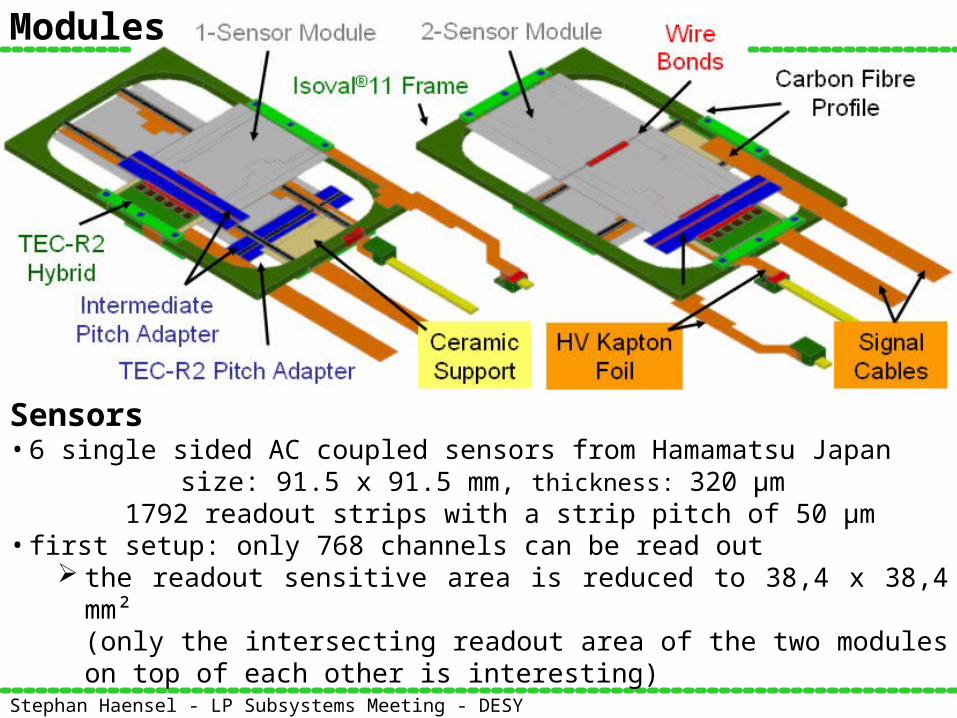
Modules
Sensors • 6 single sided AC coupled sensors from Hamamatsu Japan
size: 91.5 x 91.5 mm, thickness: 320 μm1792 readout strips with a strip pitch of 50 μm
• first setup: only 768 channels can be read out the readout sensitive area is reduced to 38,4 x 38,4 mm²
(only the intersecting readout area of the two modules on top of each other is interesting)

Stephan Haensel - LP Subsystems Meeting - DESY
Modules
Front-End Hybrids including Pitch Adapter• Start up:
hybrids leftover from the CMS Tracker End Cap module production will be usedalready assembled
and bonded• Later on:
replacement with newly developed FE chips
Stephan Haensel - LP Subsystems Meeting - DESY
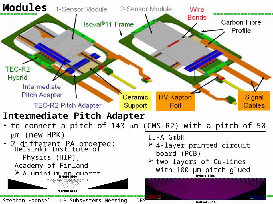
Modules
Intermediate Pitch Adapter• to connect a pitch of 143 m (CMS-R2) with a pitch of 50 m (new HPK)• 2 different PA ordered: ILFA GmbH
4-layer printed circuit board (PCB) two layers of Cu-lines with 100 μm
pitch glued staggered and shifted on top of each other
Helsinki Institute of Physics (HIP),Academy of Finland Aluminium on quartz

Stephan Haensel - LP Subsystems Meeting - DESY
Plan B - intermediate pitch adaptersPitch Adapter from HIP - 7(+2 damaged) received 7.2.08
optical inspection revealed problems on ALL PA-> problems during the production procedure
next steps:-) reprocessing from HIP-) electrical verification of the number of bad channels
if HIP-PA are not usable -> pitch adapter from ILFA will be used - 4 received 1.8.08
they are 11mm larger -> increasing module width optical inspection revealed no problems PA were electronically tested from ILFA (to be verified)
PA from HIP PA from HIP
PA from HIP
PA from HIP

Stephan Haensel - LP Subsystems Meeting - DESY
Modules
Isoval®11 FrameIsoval®11 is a composite of resin epoxy reinforced with a woven fibreglass mat• high rigidity• low mass • insulator• easy to mechanically processmodules are not glued but get clipped to the frame with 3 mm thick Isoval®11
pads which get screwed to the frame-> easy exchange of modules to enable tests of different sensors and FE chips

Stephan Haensel - LP Subsystems Meeting - DESY
Modules
HV Kapton Foil• deliver the HV bias voltage to the sensor backplane• isolate the sensor backplane from the carbon fibre profiles• modified leftovers of the CMS sensor recuperation campaign are used
they contain already RC circuits to stabilize the HV line
Wire Bonds• standardised ultrasonic wire bonding with a Delvotec 6400 automatic bonding machine• aluminium wires: 25 μm diameter including 1% silicon
Stephan Haensel - LP Subsystems Meeting - DESY
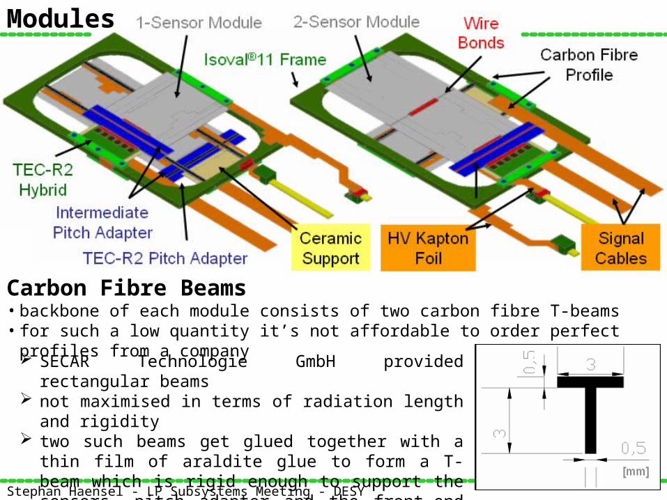
Modules
Carbon Fibre Beams• backbone of each module consists of two carbon fibre T-beams• for such a low quantity it’s not affordable to order perfect profiles from a company
SECAR Technologie GmbH provided rectangular beams not maximised in terms of radiation length and rigidity two such beams get glued together with a thin film of
araldite glue to form a T-beam which is rigid enough to support the sensors, pitch adapter and the front-end hybrid

Stephan Haensel - LP Subsystems Meeting - DESY
Moveable Support System• two aluminium sliding carriages for the silicon modules get build by IEKP
Karlsruhe– movement of the two diagonally arranged frames, containing the
silicon modules, independently in both, phi and in z direction• phi-direction: curved rails mounted at the outside of the magnet
and at the beginning of the magnets bottleneck• z-direction: the sledges move along two round rods via a
threaded rod
Rails
Stephan Haensel - LP Subsystems Meeting - DESY
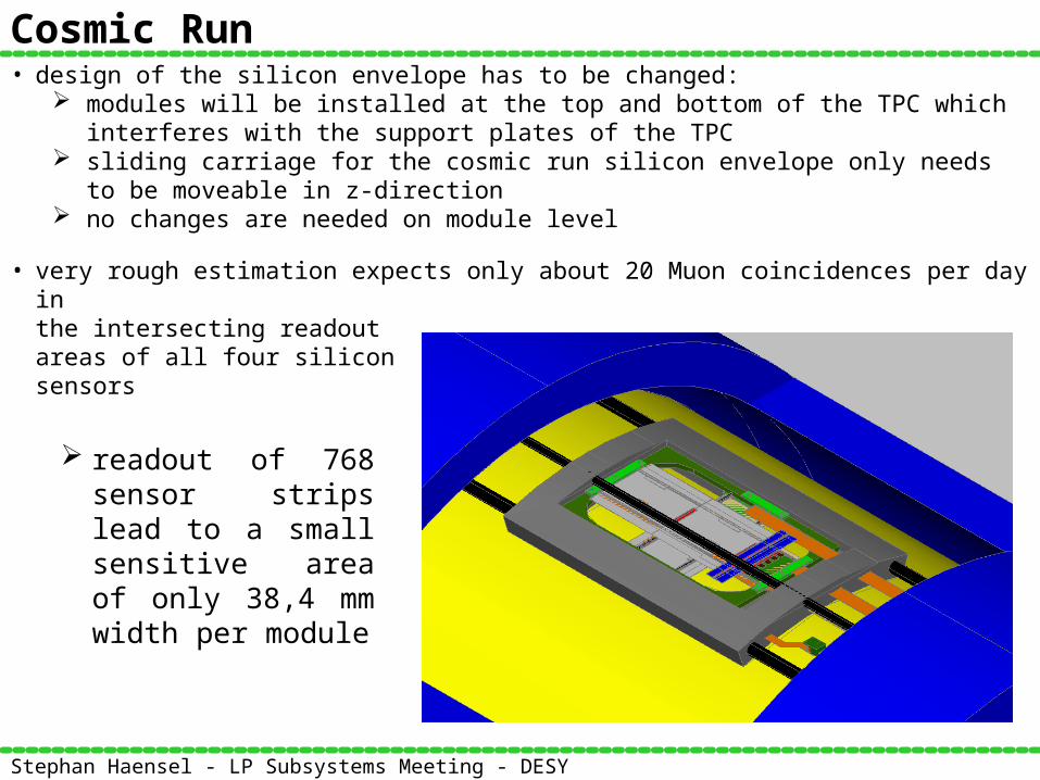
Cosmic Run• design of the silicon envelope has to be changed:
modules will be installed at the top and bottom of the TPC which interferes with the support plates of the TPC
sliding carriage for the cosmic run silicon envelope only needs to be moveable in z-direction
no changes are needed on module level
• very rough estimation expects only about 20 Muon coincidences per day inthe intersecting readout areas of all four silicon sensors
readout of 768 sensor strips lead to a small sensitive area of only 38,4 mm width per module

Stephan Haensel - LP Subsystems Meeting - DESY
Done & To Do HPK sensors passed QA tests first prototype module was already build and shipped to IEKP Karlsruhe
to make a prototype sliding carriage
• the needed space for the envelope has to be fixed in agreement with the TPC support structures quite narrow in cosmic setup ± no interference in test beam setup
• it has to be defined were the envelope support can be fixed most probable at the outside of the magnet and the beginning of the
magnets bottleneck via curved rails• sliding carriage has to be build• final modules have to be build
first intermediate PAs received but not tested gluing and bonding jigs in progress
• readout system has to be fixed CCUMs have to be found + new ICBs build or emergency plan is needed (APV - ARCs, Beetle chip - ALIBAVA)
• readout software has to be determined and combined with TPC software
Stephan Haensel - LP Subsystems Meeting - DESY
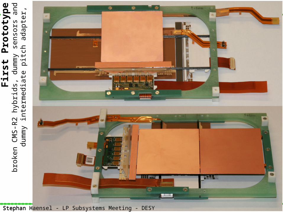
Fir
st P
roto
typ
ebr
oken
CM
S-R
2 hy
brid
s, d
umm
y se
nsor
s an
d du
mm
y in
term
edia
te p
itch
adap
ter,
Stephan Haensel - LP Subsystems Meeting - DESY

Stephan Haensel - LP Subsystems Meeting - DESY
BACKUP Slides

Stephan Haensel - LP Subsystems Meeting - DESY
HPK Sensors (6 needed for this setup)
- single-sided AC coupled SSD
- Sensor size: 91,5 x 91,5 mm² (± 0,04 mm)
- Wafer thickness: approx. 320 μm
- Resistivity: such that depletion voltage: 50 V < Vdepl < 100 Volt- Leakage current: < 10 μA per sensor
- Biasing scheme: poly-Silicon Resistor with 20 MW (± 5 MW)
- Number of strips: 1792 (= 14 x 128)
- Strip pitch: 50 μm pitch, no intermediate strips
- Strip width: 12.5 μm
- Dielectric Structure: Oxide (SiO2) + Nitride (Si3N4) between p+ and aluminium strips. (Thicknesses like for CMS)
- 2 bond pads on each side of the strip (CMS size)
- 1 probe pad on each side of the strip (contact to p+)
Wafer Layout
91,5 x 91,5 mm