status of ilc and the role of japan in developing the ilc · status of ilc and the role of japan in...
TRANSCRIPT
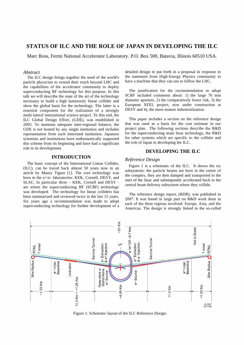
Figure 1: Schematic layout of the ILC Reference Design.
STATUS OF ILC AND THE ROLE OF JAPAN IN DEVELOPING THE ILC
Marc Ross, Fermi National Accelerator Laboratory. P.O. Box 500, Batavia, Illinois 60510 USA.
Abstract The ILC design brings together the need of the world's
particle physicists to extend their reach beyond LHC and
the capabilities of the accelerator community to deploy
superconducting RF technology for this purpose. In this
talk we will describe the state of the art of the technology
necessary to build a high luminosity linear collider and
show the global basis for the technology. The latter is a
essential component for the realization of a strongly
multi-lateral international science project. To this end, the
ILC Global Design Effort, (GDE), was established in
2005. To maintain adequate inter-regional balance, the
GDE is not hosted by any single institution and includes
representation from each interested institution. Japanese
scientists and institutions have enthusiastically supported
this scheme from its beginning and have had a significant
role in its development.
INTRODUCTION
The basic concept of the International Linear Collider,
(ILC), can be traced back almost 50 years now to an
article by Maury Tigner [1]. The core technology was
born in the e+/e- laboratories: KEK, Cornell, DESY, and
SLAC. In particular three – KEK, Cornell and DESY -
are where the superconducting RF (SCRF) technology
was developed. The technology for linear colliders has
been summarized and reviewed twice in the last 15 years.
Six years ago a recommendation was made to adopt
superconducting technology for further development of a
detailed design to put forth in a proposal in response to
the statement from High-Energy Physics community to
have a machine that they can use to follow the LHC.
The justification for the recommendation to adopt
SCRF included comments about: 1) the large 76 mm
diameter aperture, 2) the comparatively lower risk, 3) the
European XFEL project, now under construction at
DESY and 4), the more mature industrialization.
This paper includes a section on the reference design
that was used as a basis for the cost estimate in our
project plan. The following sections describe the R&D
for the superconducting main linac technology, the R&D
for other systems which are specific to the collider and
the role of Japan in developing the ILC.
DEVELOPING THE ILC
Reference Design
Figure 1 is a schematic of the ILC. It shows the six
subsystems: the particle beams are born in the centre of
the complex, they are then damped and transported to the
start of the linac and subsequently accelerated back to the
central beam delivery subsystem where they collide.
The reference design report, (RDR), was published in
2007. It was based in large part on R&D work done in
each of the three regions involved: Europe, Asia, and the
Americas. The design is strongly linked to the so-called
TESLA design that was developed in Europe using the
superconducting technology. The RDR was authored by
several hundred institutions, including 15 Japanese
institutions, among them KEK and JAEA.
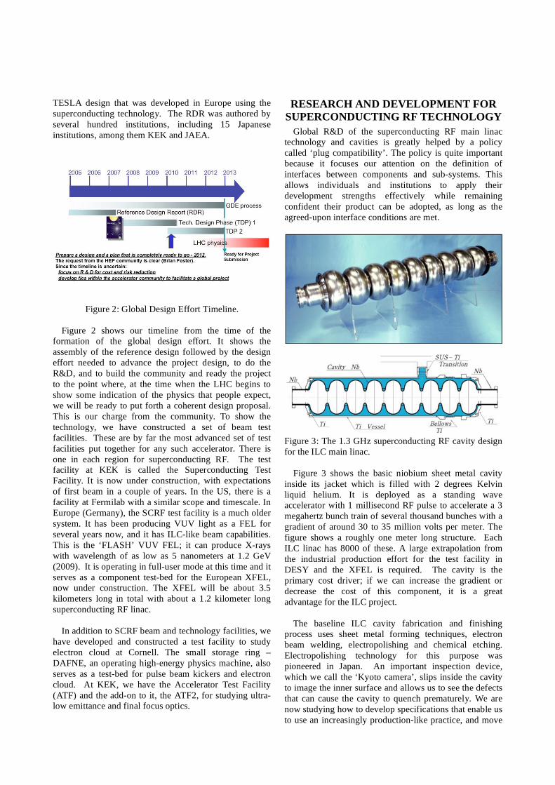
Figure 2: Global Design Effort Timeline.
Figure 2 shows our timeline from the time of the
formation of the global design effort. It shows the
assembly of the reference design followed by the design
effort needed to advance the project design, to do the
R&D, and to build the community and ready the project
to the point where, at the time when the LHC begins to
show some indication of the physics that people expect,
we will be ready to put forth a coherent design proposal.
This is our charge from the community. To show the
technology, we have constructed a set of beam test
facilities. These are by far the most advanced set of test
facilities put together for any such accelerator. There is
one in each region for superconducting RF. The test
facility at KEK is called the Superconducting Test
Facility. It is now under construction, with expectations
of first beam in a couple of years. In the US, there is a
facility at Fermilab with a similar scope and timescale. In
Europe (Germany), the SCRF test facility is a much older
system. It has been producing VUV light as a FEL for
several years now, and it has ILC-like beam capabilities.
This is the ‘FLASH’ VUV FEL; it can produce X-rays
with wavelength of as low as 5 nanometers at 1.2 GeV
(2009). It is operating in full-user mode at this time and it
serves as a component test-bed for the European XFEL,
now under construction. The XFEL will be about 3.5
kilometers long in total with about a 1.2 kilometer long
superconducting RF linac.
In addition to SCRF beam and technology facilities, we
have developed and constructed a test facility to study
electron cloud at Cornell. The small storage ring –
DAFNE, an operating high-energy physics machine, also
serves as a test-bed for pulse beam kickers and electron
cloud. At KEK, we have the Accelerator Test Facility
(ATF) and the add-on to it, the ATF2, for studying ultra-
low emittance and final focus optics.
RESEARCH AND DEVELOPMENT FOR
SUPERCONDUCTING RF TECHNOLOGY
Global R&D of the superconducting RF main linac
technology and cavities is greatly helped by a policy
called ‘plug compatibility’. The policy is quite important
because it focuses our attention on the definition of
interfaces between components and sub-systems. This
allows individuals and institutions to apply their
development strengths effectively while remaining
confident their product can be adopted, as long as the
agreed-upon interface conditions are met.
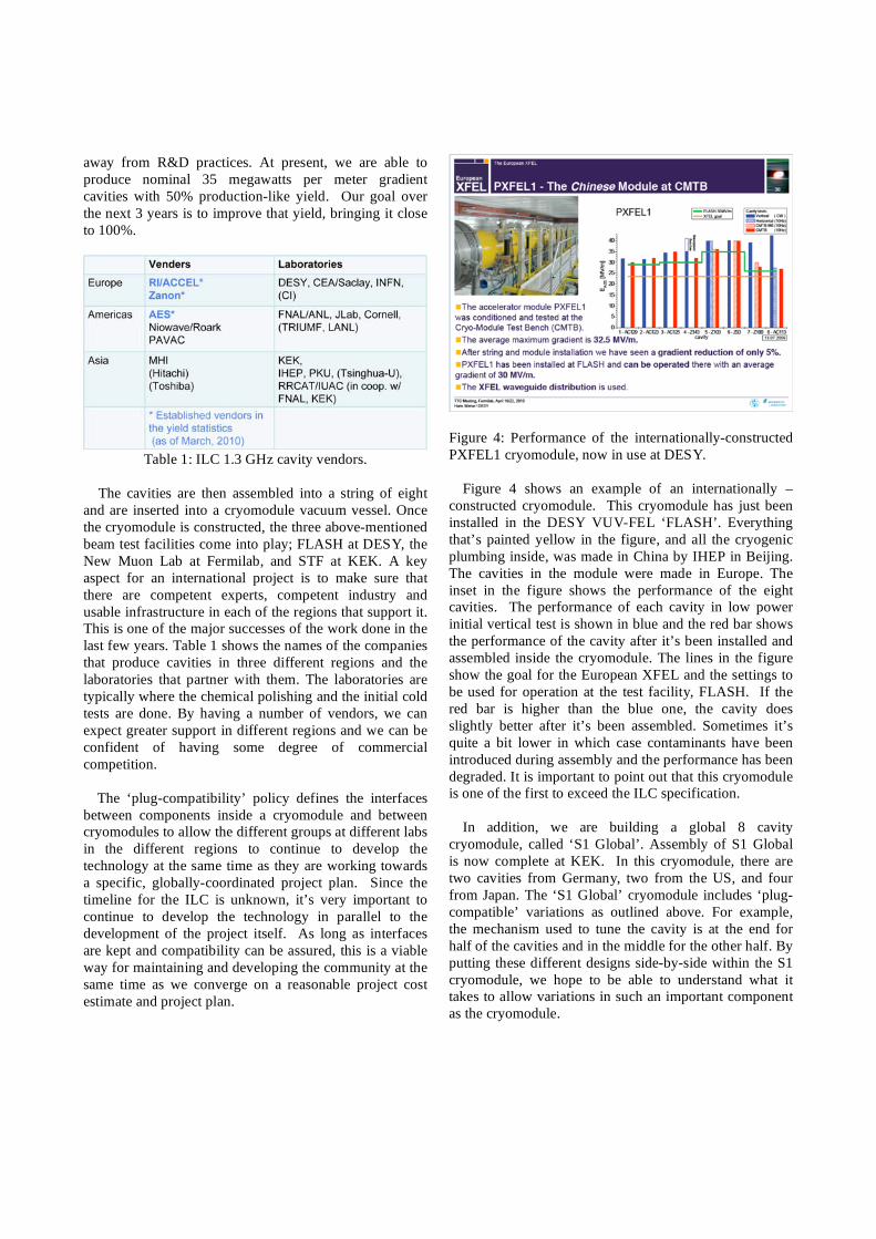
Figure 3: The 1.3 GHz superconducting RF cavity design
for the ILC main linac.
Figure 3 shows the basic niobium sheet metal cavity
inside its jacket which is filled with 2 degrees Kelvin
liquid helium. It is deployed as a standing wave
accelerator with 1 millisecond RF pulse to accelerate a 3
megahertz bunch train of several thousand bunches with a
gradient of around 30 to 35 million volts per meter. The
figure shows a roughly one meter long structure. Each
ILC linac has 8000 of these. A large extrapolation from
the industrial production effort for the test facility in
DESY and the XFEL is required. The cavity is the
primary cost driver; if we can increase the gradient or
decrease the cost of this component, it is a great
advantage for the ILC project.
The baseline ILC cavity fabrication and finishing
process uses sheet metal forming techniques, electron
beam welding, electropolishing and chemical etching.
Electropolishing technology for this purpose was
pioneered in Japan. An important inspection device,
which we call the ‘Kyoto camera’, slips inside the cavity
to image the inner surface and allows us to see the defects
that can cause the cavity to quench prematurely. We are
now studying how to develop specifications that enable us
to use an increasingly production-like practice, and move
away from R&D practices. At present, we are able to
produce nominal 35 megawatts per meter gradient
cavities with 50% production-like yield. Our goal over
the next 3 years is to improve that yield, bringing it close
to 100%.
Table 1: ILC 1.3 GHz cavity vendors.
The cavities are then assembled into a string of eight
and are inserted into a cryomodule vacuum vessel. Once
the cryomodule is constructed, the three above-mentioned
beam test facilities come into play; FLASH at DESY, the
New Muon Lab at Fermilab, and STF at KEK. A key
aspect for an international project is to make sure that
there are competent experts, competent industry and
usable infrastructure in each of the regions that support it.
This is one of the major successes of the work done in the
last few years. Table 1 shows the names of the companies
that produce cavities in three different regions and the
laboratories that partner with them. The laboratories are
typically where the chemical polishing and the initial cold
tests are done. By having a number of vendors, we can
expect greater support in different regions and we can be
confident of having some degree of commercial
competition.
The ‘plug-compatibility’ policy defines the interfaces
between components inside a cryomodule and between
cryomodules to allow the different groups at different labs
in the different regions to continue to develop the
technology at the same time as they are working towards
a specific, globally-coordinated project plan. Since the
timeline for the ILC is unknown, it’s very important to
continue to develop the technology in parallel to the
development of the project itself. As long as interfaces
are kept and compatibility can be assured, this is a viable
way for maintaining and developing the community at the
same time as we converge on a reasonable project cost
estimate and project plan.
Figure 4: Performance of the internationally-constructed
PXFEL1 cryomodule, now in use at DESY.
Figure 4 shows an example of an internationally –
constructed cryomodule. This cryomodule has just been
installed in the DESY VUV-FEL ‘FLASH’. Everything
that’s painted yellow in the figure, and all the cryogenic
plumbing inside, was made in China by IHEP in Beijing.
The cavities in the module were made in Europe. The
inset in the figure shows the performance of the eight
cavities. The performance of each cavity in low power
initial vertical test is shown in blue and the red bar shows
the performance of the cavity after it’s been installed and
assembled inside the cryomodule. The lines in the figure
show the goal for the European XFEL and the settings to
be used for operation at the test facility, FLASH. If the
red bar is higher than the blue one, the cavity does
slightly better after it’s been assembled. Sometimes it’s
quite a bit lower in which case contaminants have been
introduced during assembly and the performance has been
degraded. It is important to point out that this cryomodule
is one of the first to exceed the ILC specification.
In addition, we are building a global 8 cavity
cryomodule, called ‘S1 Global’. Assembly of S1 Global
is now complete at KEK. In this cryomodule, there are
two cavities from Germany, two from the US, and four
from Japan. The ‘S1 Global’ cryomodule includes ‘plug-
compatible’ variations as outlined above. For example,
the mechanism used to tune the cavity is at the end for
half of the cavities and in the middle for the other half. By
putting these different designs side-by-side within the S1
cryomodule, we hope to be able to understand what it
takes to allow variations in such an important component
as the cryomodule.
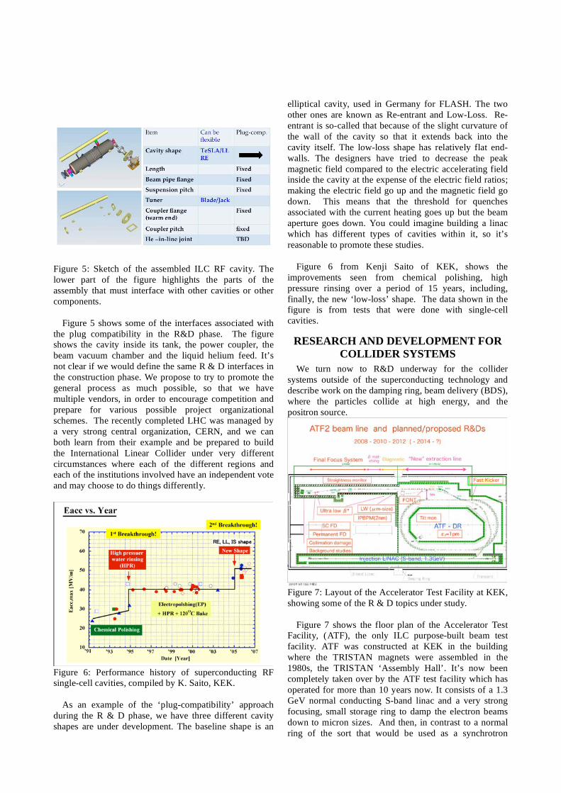
Figure 5: Sketch of the assembled ILC RF cavity. The
lower part of the figure highlights the parts of the
assembly that must interface with other cavities or other
components.
Figure 5 shows some of the interfaces associated with
the plug compatibility in the R&D phase. The figure
shows the cavity inside its tank, the power coupler, the
beam vacuum chamber and the liquid helium feed. It’s
not clear if we would define the same R & D interfaces in
the construction phase. We propose to try to promote the
general process as much possible, so that we have
multiple vendors, in order to encourage competition and
prepare for various possible project organizational
schemes. The recently completed LHC was managed by
a very strong central organization, CERN, and we can
both learn from their example and be prepared to build
the International Linear Collider under very different
circumstances where each of the different regions and
each of the institutions involved have an independent vote
and may choose to do things differently.
Figure 6: Performance history of superconducting RF
single-cell cavities, compiled by K. Saito, KEK.
As an example of the ‘plug-compatibility’ approach
during the R & D phase, we have three different cavity
shapes are under development. The baseline shape is an
elliptical cavity, used in Germany for FLASH. The two
other ones are known as Re-entrant and Low-Loss. Re-
entrant is so-called that because of the slight curvature of
the wall of the cavity so that it extends back into the
cavity itself. The low-loss shape has relatively flat end-
walls. The designers have tried to decrease the peak
magnetic field compared to the electric accelerating field
inside the cavity at the expense of the electric field ratios;
making the electric field go up and the magnetic field go
down. This means that the threshold for quenches
associated with the current heating goes up but the beam
aperture goes down. You could imagine building a linac
which has different types of cavities within it, so it’s
reasonable to promote these studies.
Figure 6 from Kenji Saito of KEK, shows the
improvements seen from chemical polishing, high
pressure rinsing over a period of 15 years, including,
finally, the new ‘low-loss’ shape. The data shown in the
figure is from tests that were done with single-cell
cavities.
RESEARCH AND DEVELOPMENT FOR
COLLIDER SYSTEMS
We turn now to R&D underway for the collider
systems outside of the superconducting technology and
describe work on the damping ring, beam delivery (BDS),
where the particles collide at high energy, and the
positron source.
Figure 7: Layout of the Accelerator Test Facility at KEK,
showing some of the R & D topics under study.
Figure 7 shows the floor plan of the Accelerator Test
Facility, (ATF), the only ILC purpose-built beam test
facility. ATF was constructed at KEK in the building
where the TRISTAN magnets were assembled in the
1980s, the TRISTAN ‘Assembly Hall’. It’s now been
completely taken over by the ATF test facility which has
operated for more than 10 years now. It consists of a 1.3
GeV normal conducting S-band linac and a very strong
focusing, small storage ring to damp the electron beams
down to micron sizes. And then, in contrast to a normal
ring of the sort that would be used as a synchrotron
radiation source, the beam is then extracted as if it were to
be injected into the main linac after compression. The
‘extraction’ or diagnostic line follows and links the ring to
the BDS test facility ATF2, recently constructed. In order
to try to focus it down to very small sizes, beam
manipulation is done and at the end. We hope to have
beam sizes on the order of a few tens of nanometers in
order to study beam handling and instrumentation.
One of the key issues with the beam facilities or each of
the beam test facilities works toward the development of
the ILC as a project but these places are also
fundamentally for students. At ATF, there are students
from these institutions from each of the three regions that
support the ILC. Approximately 2000 people-days per
year, (roughly 70 people stationed at KEK – including
collaboration members from Universities in Japan), work
at ATF. It’s an enormous international effort at KEK.
Damping Ring
There are two 6 kilometer damping rings in the ILC
design, 5 GeV each. On each pulse, 3000 bunches are
injected, and the interval between each bunch is reduced
50 times smaller than it is in the superconducting linac.
The bunches are damped to very low emittance and then
extracted one by one in order to take the 6-nanosecond
spacing to 300 nanoseconds with a fast kicker. The three
facilities, Cornell (CESR TA), Dafne (Frascati), and ATF
(KEK) support the damping ring activities. Also, there are
many aspects about the design in common with the R&D
on the ILC damping rings.
Damping Ring R&D consists of three primary
activities: 1) electron cloud collective effects and
mitigation strategies, 2) fast kicker technology and 3)
ultra-low emittance tuning. Electron cloud primarily
affects positrons, so it can’t be studied at ATF; ATF is an
electron ring. Electron cloud phenomena are under study
at these e-plus/e-minus machines, CesrTA in Cornell,
DAFNE in Italy and KEKB. Fast kickers can be studied
at ATF; it’s one of the primary topics under study at ATF
to make the pulse magnet which is capable of pulling a
bunch out with a 6-nanosecond or even perhaps a 3-
nanosecond spacing between bunches. Ultra-low
emittance tuning is needed to achieve typical beam sizes
of few microns. We would like to go to the physical
limiting emittance, beyond what has been done at light
sources, to a vertical emittance of a few picometer-radians.
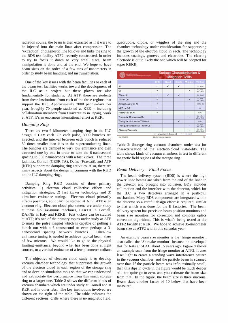
The objective of electron cloud study is to develop
vacuum chamber technology that suppresses the growth
of the electron cloud in each region of the storage ring
and to develop simulation tools so that we can understand
and extrapolate the performance from this small storage
ring to a larger one. Table 2 shows the different kinds of
vacuum chambers which are under study at Cornell and at
KEK and in other labs. The key institutions involved are
shown on the right of the table. The table indicates the
different sections, drifts where there is no magnetic field,
quadrupole, dipole, or wigglers of the ring and the
chamber technology under consideration for suppressing
the growth of the electron cloud in each. The technology
includes coatings, grooves and electrodes. The clearing
electrode is quite likely the one which will be adopted for
super KEKB.
Table 2: Storage ring vacuum chambers under test for
characterization of the electron-cloud instability. The
table shows kinds of vacuum chambers in test in different
magnetic field regions of the storage ring.
Beam Delivery – Final Focus
The beam delivery system (BDS) is where the high
power linac beams are taken from the end of the linac to
the detector and brought into collision. BDS includes
collimation and the interface with the detector, which for
the ILC is two detectors arranged in a push-pull
mechanism. Many BDS components are integrated within
the detector so a careful design effort is required, similar
to that which was done for the B factories. The beam
delivery system has precision beam position monitors and
beam size monitors for correction and complex optics
correction algorithms. This is what’s being tested at the
ATF2 facility at KEK. We hope to achieve 35-nanometer
beam size at ATF2 within this calendar year.
An example beam size monitor is the ‘fringe monitor’,
also called the ‘Shintake monitor’ because he developed
this for tests at SLAC about 15 years ago. Figure 8 shows
an example scan from the fringe monitor at ATF2. It uses
laser light to create a standing wave interference pattern
in the vacuum chamber, and the particle beam is scanned
over that. If the particle beam was infinitesimally small,
then this dips in cycle in the figure would be much deeper,
still not quite go to zero, and you estimate the beam size
from that. In the figure, the beam size is three microns.
Beam sizes another factor of 10 below that have been
measured.
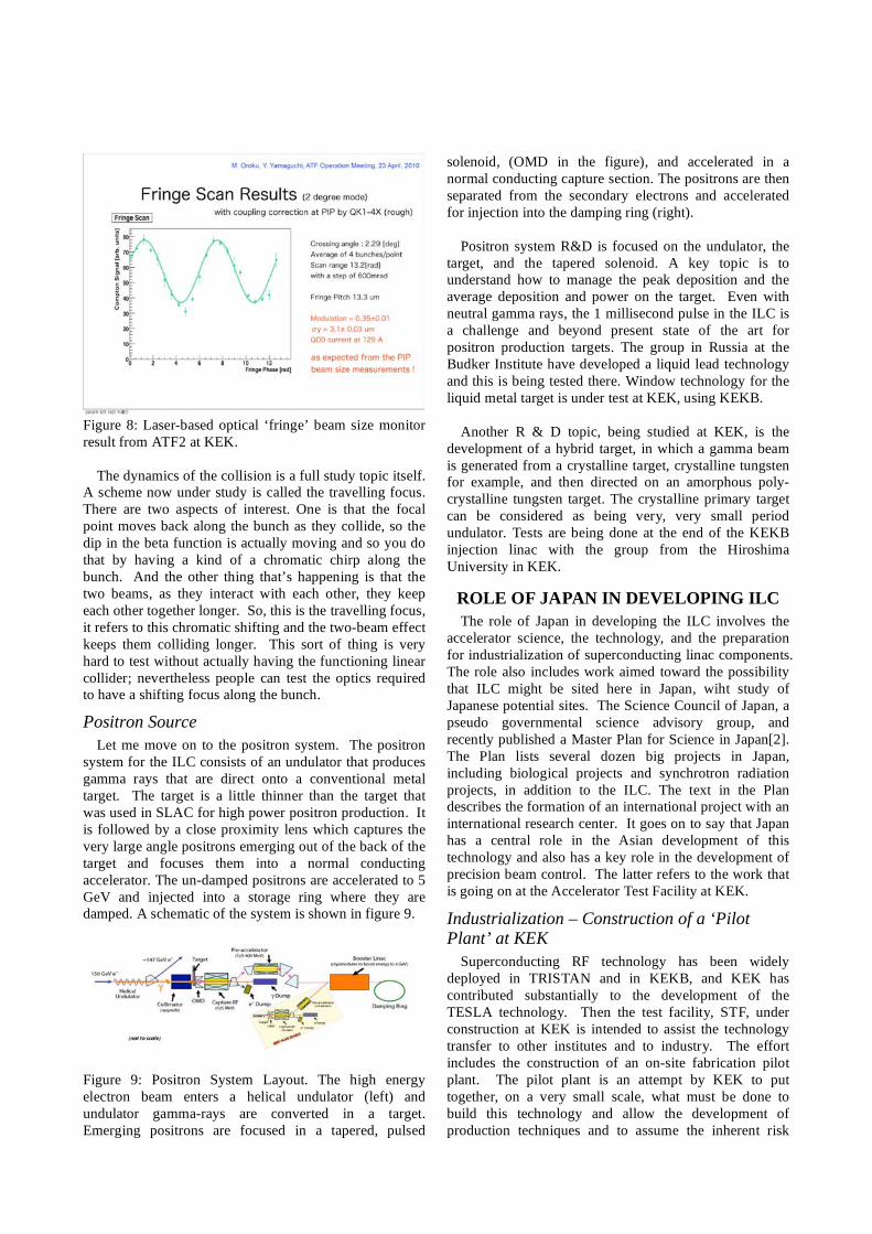
Figure 8: Laser-based optical ‘fringe’ beam size monitor
result from ATF2 at KEK.
The dynamics of the collision is a full study topic itself.
A scheme now under study is called the travelling focus.
There are two aspects of interest. One is that the focal
point moves back along the bunch as they collide, so the
dip in the beta function is actually moving and so you do
that by having a kind of a chromatic chirp along the
bunch. And the other thing that’s happening is that the
two beams, as they interact with each other, they keep
each other together longer. So, this is the travelling focus,
it refers to this chromatic shifting and the two-beam effect
keeps them colliding longer. This sort of thing is very
hard to test without actually having the functioning linear
collider; nevertheless people can test the optics required
to have a shifting focus along the bunch.
Positron Source
Let me move on to the positron system. The positron
system for the ILC consists of an undulator that produces
gamma rays that are direct onto a conventional metal
target. The target is a little thinner than the target that
was used in SLAC for high power positron production. It
is followed by a close proximity lens which captures the
very large angle positrons emerging out of the back of the
target and focuses them into a normal conducting
accelerator. The un-damped positrons are accelerated to 5
GeV and injected into a storage ring where they are
damped. A schematic of the system is shown in figure 9.
Figure 9: Positron System Layout. The high energy
electron beam enters a helical undulator (left) and
undulator gamma-rays are converted in a target.
Emerging positrons are focused in a tapered, pulsed
solenoid, (OMD in the figure), and accelerated in a
normal conducting capture section. The positrons are then
separated from the secondary electrons and accelerated
for injection into the damping ring (right).
Positron system R&D is focused on the undulator, the
target, and the tapered solenoid. A key topic is to
understand how to manage the peak deposition and the
average deposition and power on the target. Even with
neutral gamma rays, the 1 millisecond pulse in the ILC is
a challenge and beyond present state of the art for
positron production targets. The group in Russia at the
Budker Institute have developed a liquid lead technology
and this is being tested there. Window technology for the
liquid metal target is under test at KEK, using KEKB.
Another R & D topic, being studied at KEK, is the
development of a hybrid target, in which a gamma beam
is generated from a crystalline target, crystalline tungsten
for example, and then directed on an amorphous poly-
crystalline tungsten target. The crystalline primary target
can be considered as being very, very small period
undulator. Tests are being done at the end of the KEKB
injection linac with the group from the Hiroshima
University in KEK.
ROLE OF JAPAN IN DEVELOPING ILC
The role of Japan in developing the ILC involves the
accelerator science, the technology, and the preparation
for industrialization of superconducting linac components.
The role also includes work aimed toward the possibility
that ILC might be sited here in Japan, wiht study of
Japanese potential sites. The Science Council of Japan, a
pseudo governmental science advisory group, and
recently published a Master Plan for Science in Japan[2].
The Plan lists several dozen big projects in Japan,
including biological projects and synchrotron radiation
projects, in addition to the ILC. The text in the Plan
describes the formation of an international project with an
international research center. It goes on to say that Japan
has a central role in the Asian development of this
technology and also has a key role in the development of
precision beam control. The latter refers to the work that
is going on at the Accelerator Test Facility at KEK.
Industrialization – Construction of a ‘Pilot Plant’ at KEK
Superconducting RF technology has been widely
deployed in TRISTAN and in KEKB, and KEK has
contributed substantially to the development of the
TESLA technology. Then the test facility, STF, under
construction at KEK is intended to assist the technology
transfer to other institutes and to industry. The effort
includes the construction of an on-site fabrication pilot
plant. The pilot plant is an attempt by KEK to put
together, on a very small scale, what must be done to
build this technology and allow the development of
production techniques and to assume the inherent risk

associated. It is quite an interesting way to partner with
the companies involved.
The pilot plant is operated by the accelerator laboratory
with participation of collaborating companies. The tests
and development done there can be spun off to the
different companies. Figure 10 shows the floor plan. It is
now under construction and will begin work at the end of
next year, 2011. There is an electron beam welder,
chemical polishing room, and machinery needed for
cavity fabrication. It is located in a building in KEK
which was formerly used for the power supplies for the
Proton Synchrotron.
Figure 10: KEK superconducting RF cavity pilot plant
floor plan.
Civil Engineering
Civil construction is a large fraction of the anticipated
cost of ILC. For our reference design, we studied three
sample sites, one in Japan, one at CERN, and one very
near Fermilab. The three are quite similar deep rock sites.
Recently, we began work on a very different site which is
in Dubna, Russia, near the Joint Institute for Nuclear
Research. We will use it for comparison to show how we
would optimize the civil construction layout of a different
site. With that same process in mind, we are now
considering a mountain site with the participation of
Japanese general contractors through the ‘Association for
the Advancement of Accelerators’.
Figure 11: Site configuration cross-sections.
CONCLUSION
The global design effort is supported by the three
project managers, each one having a very different
background, and our coming together symbolizes the
international nature of the project. My Co-Project
Manager, Akira Yamamoto, was awarded the Nishina
Prize for the observation of cosmic anti-protons in 2000.
Our effort has three goals. The first one is a community
goal, aimed at developing communication channels and
connections. The second is to do the design and
development work, and the third is to put together a
project plan. This should be done by the end of 2012. I
have tried to show that the Japanese contributions to ILC
development span the entire complex and cover both the
R&D and the design, and the industrial and technical
components.
ACKNOWLEDGEMENTS
This presentation was made on behalf of my colleagues,
Nick Walker from DESY and Akira Yamamoto from
KEK.
REFERENCES
[1] Tigner, Nuovo Cimento 37 (1965).
[2] Master Plan for Science in Japan, 2009
Figure 11 shows cross-sections of different types of
sites. The circled cross-sections are under development
and were either described in the reference design or have
been developed since it was published. Here it shows
what a mountain site might look like. The figure shows
the type of site that was studied in the very flat ground
near the Joint Institute, north of Moscow. It also shows a
sample site, in a Japanese mountain range, showing the
tunnel and the different ways that the main tunnel would
be connected to the surface.