standard product reference sheet hcnw115ajte-tr features
TRANSCRIPT

HCNW115AJTE-TR
CLCC type
Outer dimension: 3.0 x 2.5 x 0.77mm ( L x W x H )
・Adjusted to Automotive lighting standards
・High reliability, High flux, Low thermal resistance package
・Suitable light source for outer lens which is designed by customer
Emitting area : 1mm square
・Lead-free soldering compatible
・RoHS compliant
Package
Product features
Recommended Applications
Features
・Exterior light source for Automotive, motorcycle (Head lamp, DRL, Cornering lamp, Fog lamp, etc.)
・LED flood light
・Light source for other equipment
Standard Product Reference Sheet
Page : 1 2016.11.25

HCNW115AJTE-TR Outline Dimensions
Unit :mm
Weight :20.0mg
Tolerance :±0.2
Page : 2
Emission size
0.98 Laser Marking area
Cathode Mark
①,③,④
②
⑥
⑤
Height of emission
⑦ Anode ⑦ Cathode
Inside circuit
Cathode Anode
Top view Side view Bottom view
Cross section
No. Part name Material Qty.
① LED Die InGaN 1
② Protection Diode Si 1
③ Encapsulant Silicone Resin + Phosphor 1
④ Glass plate Silicone dioxide 1
⑤ Encapsulant Silicone resin 1
⑥ Lamp housing Glass ceramic 1
⑦ Electrode Au plating Anode:1 Cathode:2
2016.11.25

HCNW115AJTE-TR Recommended soldering Pattern
Unit:mm
Page : 3
Recommended solder temp.
measurement point
Cu pattern
Solder resist
Solder stencil apertural area
Recommended solder stencil
thickness:150μm
2016.11.25

HCNW115AJTE-TR Specifications
IF Derate Linearly from "Tj=125"
260
TYP. MAX.
3.0 3.9
Forward Current
mA
Tsld
ΔIF 8.0 mA/
【 Thermal Characteristics 】
Notes1
Notes1
Notes2
Notes4注1
Storage Temperature Tstg
Electro Static Discharge Threshold
"HBM"(Ta=25)ESD ±8,000 V
-40 ~ +125
-40 ~ +125
Pd
White
InGaN
White
【 Product Overview 】
LAMP HOUSING COLOR
DIE MATERIAL
EMITTING COLOR
EMISSION AREA COLOR Yellow
ITEM SYMBOL MAXIMUM RATINGS UNITS
mW
100~1,200 mA
5,016
(Ta=25)【 Absolute Maximum Ratings 】
Power Dissipation
SYMBOLITEM
Topr
Repetitive Peak Forward Current "1ms, 1/20duty" IFRM 2,000
IF
UNITS
The range of operating and storage temperature are not taping condition.
ESD testing method:EIAJ4701/300(304) Human Bodu Model (HBM) 1.5kΩ,100pF
Notes1
Notes2
Thermal resistance 【Junction - Solder point】 Rth(j-s) /W
Notes3 Please refer to page 25, "Reliability test results".
Junction Temperature Tj 150
Operating Temperature
Soldering Temperature "Reflow Soldering"
Notes4 Please refer to page 11, "Soldering Conditions".
Notes3
Page : 4 2016.11.25

HCNW115AJTE-TR Specifications
-
Notes6
Notes5
Notes5,7Chromaticity Coordinates
CxIF = 1,000mA
- 0.326 -
Cy -
Average color rendering index Ra IF = 1,000mA - 67 -
-deg.
Δθy - 117(y-dir) -Half Intensity Angle
ΔθxIF = 1,000mA
- 117(x-dir)
0.335
【 Electro-Optical Characteristics 】
Forward Voltage
MIN. TYP. MAX.
3.25 V
UNITS
VF 3.75
(Ta=25)
IF = 1,000mA Notes5
Notes8
V
φv IF = 1,000mA
2.75
VR
Luminouse Flux 265 310 410 lm
Reverse Voltage
CONDITIONSITEM SYMBOL
Not designed for reverse operation
Page : 5
x direction
y direction
Note5 Refer to the attached sheets for each sorting chart.
Note6 Do not input reverse voltage and reverse current for prevent the destruction.
Note7 Chromaticity are according to CIE1931.
Note8 Full width of viewing angle at half maximum of IV. x direction and y direction are as shown in the figure below.
2016.11.25

HCNW115AJTE-TR Specifications
Page : 6
LEDs shall be sorted out into the following chart and each rank shall be packed separately for shipping.
Rank
Luminous Flux
ΦV (lm) Conditions
C 280 300
MIN. MAX.
B 265 280
IF=1,000mA
Ta=25D 300 330
E 330 370
F 370 410
Notes
Tolerance On Luminous Flux : ±7%
Measurement Timing : Instantly After Lighting
【 Sorting chart For Luminous Flux : Φv 】
Rank
Forward Voltage
VF (V) Conditions
MIN. MAX.
A
Tolerance On Forward Voltage : ±0.1V
Measurement Timing : Instantly After Lighting
C 3.25 3.50
D 3.50 3.75
2.75 3.00
IF=1,000mA
Ta=25
B 3.00 3.25
【 Sorting Chart For Forward Voltage : VF 】
LEDs shall be sorted out into the following chart and each rank shall be packed separately for shipping.
Notes
2016.11.25

HCNW115AJTE-TR
0.275
0.325
0.375
0.275 0.325 0.375
Specifications
Page : 7
0.00
0.10
0.20
0.30
0.40
0.50
0.60
0.70
0.80
0.90
0.00 0.10 0.20 0.30 0.40 0.50 0.60 0.70 0.80 0.90
0
0.1
0.2
0.3
0.4
0.5
0.6
0.7
0.8
0.9
0 0.1 0.2 0.3 0.4 0.5 0.6 0.7 0.8 0.9
Rank x y Rank x y Rank x y
0.3213 0.3421 0.3300 0.3554 0.3380 0.3615
0.3232 0.3138 0.3302 0.3269 0.3374 0.3422
0.3178 0.3037 0.3232 0.3138 0.3302 0.3269
0.3145 0.3301 0.3213 0.3421 0.3300 0.3554
A B C
(IF=1,000mA Ta=25)
Notes
Chromaticity Coordinates Tolerance:±0.01
Measurement timing:Instantly after lighting
【 Sorting chart for Chromaticity : Cx , Cy 】 LED's shall be sorted out into the following chart and each rank shall be packed separately for shipping.
CIE Chromaticity diagram CIE Chromaticity diagram (Enlarged view)
A
B
C
ECE No.48
White area
Planckian
(BBL)
2016.11.25

HCNW115AJTE-TR
0
50
100
-100 -90 -80 -70 -60 -50 -40 -30 -20 -10 0 10 20 30 40 50 60 70 80 90 100
x
y
0.0
0.2
0.4
0.6
0.8
1.0
1.2
380 430 480 530 580 630 680 730 780
Relative Intensity vs. wavelength Condition: Ta = 25, IF =1,000mA
Wavelength (nm)
Spatial Distribution Condition: Ta = 25, IF=1,000mA
Relative Radiant Intensity (%)
Technical Data R
elat
ive
Inte
nsi
ty
x direction
y direction
Page : 8
100 50 0 50 100
0
30
60
90
-30
-60
-90
2016.11.25

HCNW115AJTE-TR
-0.4
-0.3
-0.2
-0.1
0.0
0.1
0.2
0.3
0.4
0 50 100 150
0.4
0.6
0.8
1.0
1.2
1.4
0 50 100 150
0.0
0.2
0.4
0.6
0.8
1.0
1.2
100 200 300 400 500 600 700 800 900 1,000 1,100 1,200
100
200
300
400
500
600
700
800
900
1,000
1,100
1,200
2.6 2.7 2.8 2.9 3.0 3.1 3.2 3.3 3.4 3.5
Junction Temp. vs. ΔVF
Condition : IF=1,000mA
Junction Temp. Tj ()
Rel
ativ
e L
um
inou
s F
lux
Junction Temp. vs. Relative Luminous Flux Condition : IF=1,000mA
Junction Temp. Tj ()
Rel
ativ
e L
um
inou
s F
lux
Forward Voltage vs. Forward Current Condition: Ta = 25
Forward Voltage VF (V)
Forw
ard
Cu
rren
t I F
(m
A)
ΔV
F :
(V
)
Technical Data
Forward Current vs. Relative Luminous Flux Condition : Ta = 25
Forward Current IF (mA)
Page : 9 2016.11.25

HCNW115AJTE-TR
0.30
0.31
0.32
0.33
0.34
0.35
0.30
0.31
0.32
0.33
0.34
0.35
0 50 100 150
Cx
Cx
Cy
0.31
0.32
0.33
0.34
0.35
0.36
0.31
0.32
0.33
0.34
0.35
0.36
100 300 500 700 900 1,100
Cx
Cx
Cy
Junction Temp. vs. Chromaticity Condition : IF=1,000mA
Junction Temperature Tj ()
Forward Current vs. Chromaticity Condition: Ta = 25
Forward Current IF (mA)
Technical Data
Page : 10 2016.11.25
0
100
200
300
400
500
600
700
800
900
1,000
1,100
1,200
1,300
-20 0 20 40 60 80 100 120 140 160
Max. Forward Current vs. Ambient Temp.
Junction Temperature : Tj ()
Max
imu
m F
orw
ard
Cu
rren
t :
I FM
AX
(m
A)

HCNW115AJTE-TR Soldering condition
1. Heat stress during soldering will influence the reliability of LEDs, however that effect will vary on heating
method. Also, if components of varying shape are soldered together, it is recommended to set the soldering
pad temperature according to the component most vulnerable to heat (e.g., surface mount LED).
2. LED parts including the resin are not stable immediately after soldering ( when they are not at room
temperature), any mechanical stress may cause damage to the product. Please avoid such stress after
soldering, especially stacking of the boards which may cause the boards to warp and any other types of
friction with hard materials.
3. Recommended temperature profile for the Reflow soldering is listed as the temperature of the resin
surface. Temperature distribution varies on heating method, PCB material, other components in the
assembly, and mounting density .
Please do not repeat the heating process in Reflow process more than twice.
4. When using a metal PCB, the solder may crack and problems may occur due to major stress on the soldered
portion caused by thermal shock. Please carry out a thorough advance verification before use. For the metal
PCB's insulation, it is recommended to use stress-reducing materials
Note 1 Temperature Profile for the reflow should be set to the surface temperature of resin which is on the
top of LED. This should be the maximum temperature for soldering. Lowering the heating temperature and
decreasing heating time is very effective in achieving higher reliability.
Note 2 The reflow soldering process should be done up to twice(2 times Max). When second process is
performed, interval between first and second process should be as short as possible to prevent absorption of
moisture to resin of LED. The second soldering process should not be done until LEDs have returned to room
temperature (by nature-cooling) after first soldering process.
【Soldering Precaution】
(acc.to EIAJ-4701/300)
【Recommended Reflow Soldering Condition 】
40sec MAX.
150~180
+1.5~+5/s
260MAX.
-1.5~-5/s
120sec
(Pre-heating)
(Soldering)
230
Peak Temperature
Page : 11 2016.11.25
HCNW115AJTE-TR Soldering condition
4. If soldering manually, Stanley recommends using a soldering iron equipped with temperature control. During
the actual soldering process, make sure that the soldering iron never touches the LED itself, and avoid the
LED's electrode heating temperature reaching above the heating temperature of the solder pad. All repairs
must be performed only once in the same spot, and please avoid reusing components.
5. In soldering process, immediately after iron tip is cleaned, please make sure that the soldering iron reaches the
appropriate temperature, before using. Also, please avoid applying any types of pressure to the soldered
components before the solder has been cooled and hardened, as it may deteriorate solder performance and
solder quality.
6. When using adhesive material for tentative fixatives, thermosetting resin or Ultraviolet radiation (UV) setting
resin with heat shall be recommended.
7. Flow soldering (dip soldering) is not recommended for this product.
8. Isopropyl alcohol is recommended for cleaning. Some chemicals, including Freon substitute detergent could
corrode the lens or the casing surface, which cause discoloration, cloud, crack and so on. Please review the
reference chart below for cleaning. If water is used to clean (including the final cleaning process), please use
pure water (not tap water), and completely dry the component before using.
《The curing condition, Temperature:150Max./Time:120sec.Max.》
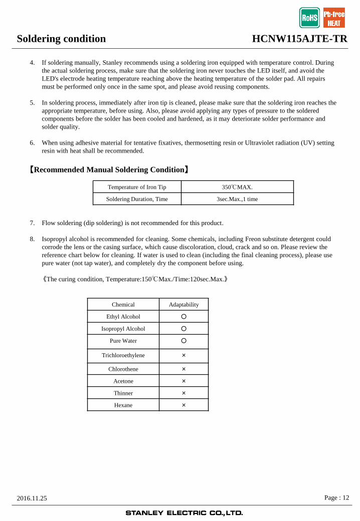
【Recommended Manual Soldering Condition】
Temperature of Iron Tip 350MAX.
Soldering Duration, Time 3sec.Max.,1 time
Chemical Adaptability
Ethyl Alcohol
Isopropyl Alcohol
Pure Water
Trichloroethylene ×
Chlorothene ×
Acetone ×
Thinner ×
Hexane ×
Page : 12 2016.11.25
HCNW115AJTE-TR Handling Precaution
LED with an InGaN die is sensitive to voltage surges generated by On/Off status change and friction with
synthetic materials, which may cause severe damage to the die or undermine its reliability. Damaged products may
experience conditions such as extremely high reverse voltage, decrease of forward rise voltage, deterioration in
optical characteristics.
Stanley InGaN products are packed with anti-static components. However, following precautions must be taken
into account upon product shipment.
① Do not place electrified non-conductive materials near the LED product.
Avoid LED products from coming into contact with metallic materials.( Should the metallic material be
electrified , the sudden surge voltage will most likely damage the product.)
② Avoid a working process which may cause the LED product to rub against other materials.
③ Install ground wires for any equipment, where they can be installed, with measures to avoid static electricity
surges.
④ Prepare a ESD protective area by placing a Conductive Mattress (1MΩ MAX.) and Ionizer to remove any
static electricity.
⑤ Operators should wear a protective wrist-strap.
⑥ Operators should wear conductive work-clothes and shoes.
⑦ To handle the products directly, Stanley recommends the use of ceramic, and not metallic, tweezers.
2. Working Environment
① A dry environment is more likely to cause static electricity. Although a dry environment is ideal for
storage state of LED products, Stanley recommends an environment with approximately 50% humidity
after the soldering process.
② Recommended static electricity level in the working environment is 150V, which is the same value as
Integrated Circuits (which are sensitive to static electricity).
【For Electric Static Discharge ( ESD)】
1. Electrification/Static Electricity protection
In order to avoid product (die) damage from static electricity caused by unprotected handling by operator and
other charged materials coming in contact with the product, Stanley recommends taking the following precautions.
Page : 13 2016.11.25
HCNW115AJTE-TR Handling Precaution
【Other Precautions】
1. The products are designed to achieve higher performance reliability, however, they can be influenced by usage
conditions.
2. Absolute maximum ratings are set to prevent LED products from breaking due to extreme stress (temperature,
current, voltage, etc.). These ratings must never be overrun even for a moment.
3. To achieve the highest performance reliability, it is necessary to take into account, factors such as forward voltage
adjusted to the usage temperature condition, derating of the power consumption, and other variable factors.
4. Please insert Straight Protective Resistors into the circuit in order to stabilize LED operation and to prevent the
device from overheating.
5. Also please make sure there isn't any gas in the surrounding area or entering from outside when using the products.
6. Please avoid to stick foreign materials because molding resin in the products has adhesiveness. And please do not
touch emission area..
7. Supersonic wave welding is not recommended because wire open circuit may occur.
ex) bonding outer lens to this product or housing
8. Please check the actual performance in the assembly because the specification sheets are described
only for LED device.
9. Please refrain from looking directly at the light source of the LED at high output, as it may harm your vision.
10. The products are designed to perform without failure in the recommended usage conditions.
However, please take the necessary precautions to prevent from a fire, injury, and other unexpected failures.
11. The products are manufactured to be used for ordinary electronic equipment. Please contact our sales staff
beforehand when exceptional quality and reliability are required, and the failure or malfunction
of the products might directly jeopardize life or health ( such as for airplanes, aerospace, medical applications,
nuclear reactor control systems and so on).
12. The formal specification sheets shall be exchanged and signed by both parties.
Page : 14 2016.11.25

HCNW115AJTE-TR
1. Picking up point with nozzle: Lamp housing of the product (Shown below)
<Recommendation>
2. Recommended Nozzle Shape
Handling Precaution
【Handling Precautions for Product Mounting】
Lens portion is the state of the hollow
Pick up point. (Lamp housing portion)
Non allowed pick up area (Lens portion)
Outside diameter : φ3.5mm
Inside diameter : φ1.7mm
The picking up point should be within lamp housing portion, because the silicone resin used for the lens is
soft. (If the nozzle makes contact with the lens, the products might be destroyed)
Please adjust the load, the pick up point, the nozzle diameter, etc. before mounting because the
over load can cause the breakage of the lamp housing.
Load : less than 3N (to avoid the product breaking)
Page : 15 2016.11.25
HCNW115AJTE-TR
This product is baked (moisture removal) before packaging, and is shipped in moisture-proof packaging (as shown
below) to minimize moisture absorption during transportation and storage. However, with regard to storing the
products, Stanley recommends the use of dry-box under the following conditions is recommended. Moisture-proof
bag as the packaging is made of anti-static material but packaging box is not.
This product is equivalent to IPC/JEDEC J-STD-020D MSL 2.
The package should not be opened until immediately prior to its use.
If any components should remain after their use, please seal the package and store them under the conditions
described in the above 【 Recommended Storage Condition 】.
Baking process should be performed after putting out from package.
Baking conditions: 10h(min.), at +60±5 just before use
Baking may be performed in the tape-reel form, however if it is performed with the reel stacked over one another,
it may case deformation
of the reels and taping materials, which may cause problems during production.
Please make sure that the product has cooled to normal temperature after performing the baking process.
Provided that, baking process shall be 2 times MAX.
【Time elapsed after Package Opening】
In the case of the package unopened , 6 months under 【 Recommended Storage Condition 】.
Please avoid rapid transition from low temp. condition to high temp. condition
and storage in corroding and dusty environment.
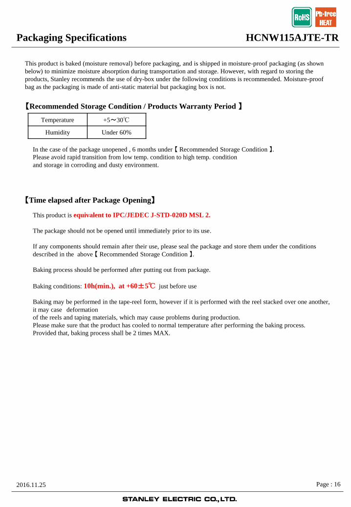
【Recommended Storage Condition / Products Warranty Period 】
Temperature +5~30
Humidity Under 60%
Page : 16
Packaging Specifications
2016.11.25

HCNW115AJTE-TR
【Moisture-proof Packaging Specification】
Fastener for re-storage
after opening bag.
Customer's opening position.
Product Label
Desiccant with indicator for
moisture level is enclosed. 1
A
Packaging Specifications
Heat Sealing position (after product being put in)
Yes No
Yes No
Yes No
Baking LED under recommended condition
Product Mounting
Unused-product remained
Return to moisture-proof package and seal Finished
Reopen the moisture-proof package
Flow chart:Package Opening to Mounting
Stored under recommended condition
Moisture-proof package first time opening
Allowable leaving time exceeded (*)
Discoloration of silica gel
Allowable leaving time means the
maximum allowable leaving time after
opening package, which depends on each
LED type.
The allowable leaving time should be
calculated form the first opening of package
to the time when soldering process is
finished.
When judging if the allowable leaving time
has exceeded or not, please subtract the
soldering time. The allowable leaving time
after reopening should be calculated form
the first opening of package, or from the
time when baking process is finished.
【Flow Chart-package Opening to Mounting】
NO. PART NAME MATERIALS REMARKS
① Moisture-proof bag
with Aluminum layer
PET+Al+PE with ESD
protection
Page : 17 2016.11.25

HCNW115AJTE-TR
【Packing box】
( RoHS・ELV Compliant )
The above measure is all the reference value.
The box is selected out of the above table by shipping quantity.
Packaging Specifications
Box TYPE Outline dimension
L × W × H (mm) Capacity of the box
Type A 280 × 265 × 45 3 reel
Type B 310 × 235 × 265 15 reel
Type C 440 × 310 × 265 30 reel
Type A
Material / box : Cardboard C5BF
Type B,C
Material / box : Cardboard K5AF
Partition : Cardboard K5AF
NO. PART NAME MATELRIAL REMARKS
② Packing BoxCorrugated
Cardboard
without ESD
protection
Page : 18 2016.11.25

HCNW115AJTE-TR
【Label Specification】
(acc.to JIS-X0503(Code-39))
Product label
A. Parts number
B. Bar-code for parts number
C. Parts code (In-house identification code for each parts number)
D. Packed parts quantity
E. Bar-Code for packed parts quantity
F. Lot number & Rank
(Please refer to Lot Number Notational System for details )
G. Bar-Code for Lot number & Rank
Opto device label
A. Customer Name
B. Parts Type
C. Parts Code
D. Parts Number
E. Packed Parts Quantity
F. Carton Number
G. Shipping Date
H. Bar-Code for In-house identification Number
<Remark> Bar-code font : acc.to Code-39(JIX0503)
Packaging Specifications
B
A
Page : 19 2016.11.25
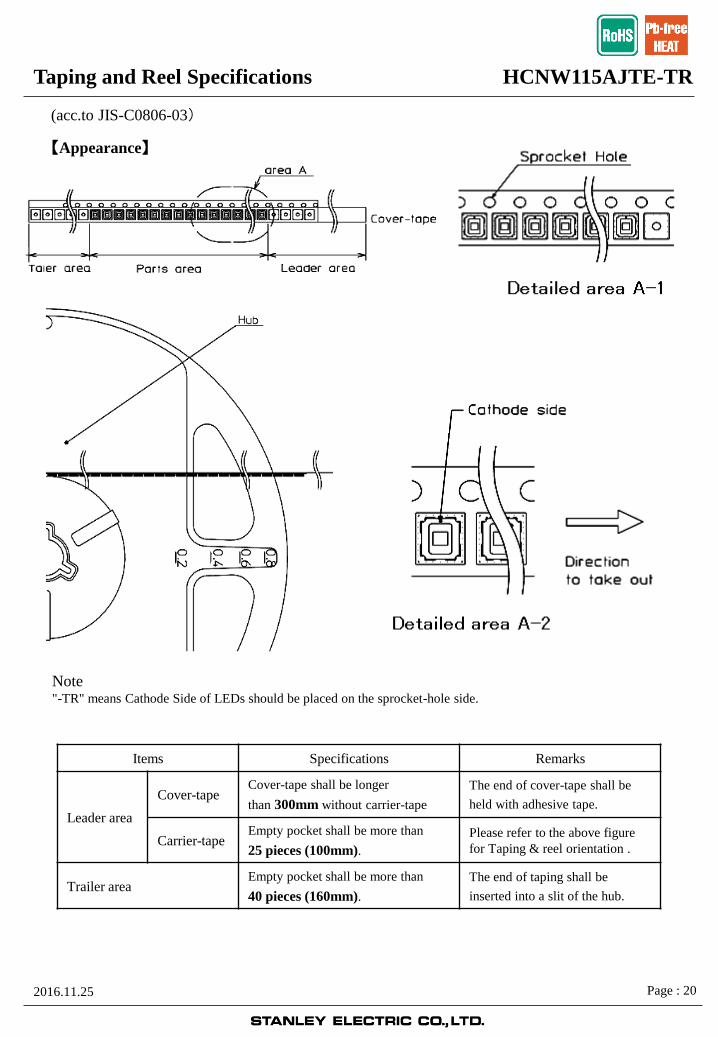
HCNW115AJTE-TR Taping and Reel Specifications
(acc.to JIS-C0806-03)
【Appearance】
Note "-TR" means Cathode Side of LEDs should be placed on the sprocket-hole side.
Items Specifications Remarks
Leader area
Cover-tape Cover-tape shall be longer
than 300mm without carrier-tape
The end of cover-tape shall be
held with adhesive tape.
Carrier-tape Empty pocket shall be more than
25 pieces (100mm).
Please refer to the above figure
for Taping & reel orientation .
Trailer area Empty pocket shall be more than
40 pieces (160mm).
The end of taping shall be
inserted into a slit of the hub.
Page : 20 2016.11.25
HCNW115AJTE-TR Taping and Reel Specifications
(acc.to JIS-C0806-03)
【 Qty. per Reel】
【Mechanical strength】
【 Others】
3,000parts/reel
Minimum Qty. per reel might be 500 parts when getting less than 3,000 parts. In such case, parts of 100-unit-qty.
Shall be packed in a reel and the qty. shall be identified on the label
Cover-tape adhesive strength shall be 0.1~1.3N ( An angle between carrier-tape and cover-tape shall be170 deg. ).
Both tapes shall be so sealed that the contained parts will not come out from the tape when it is bent at a radius of
15mm.
Reversed-orientation, Up-side down placing, side placing and out of spec. parts mix shall not be held.
Empty Pocket per reel is assumed until 1 piece.
Page : 21 2016.11.25

HCNW115AJTE-TR
【Taping Dimensions】
【Reel Dimensions】
Taping and Reel Specifications
(acc.to JIS-C0806-03) Unit :mm
Page : 22 2016.11.25
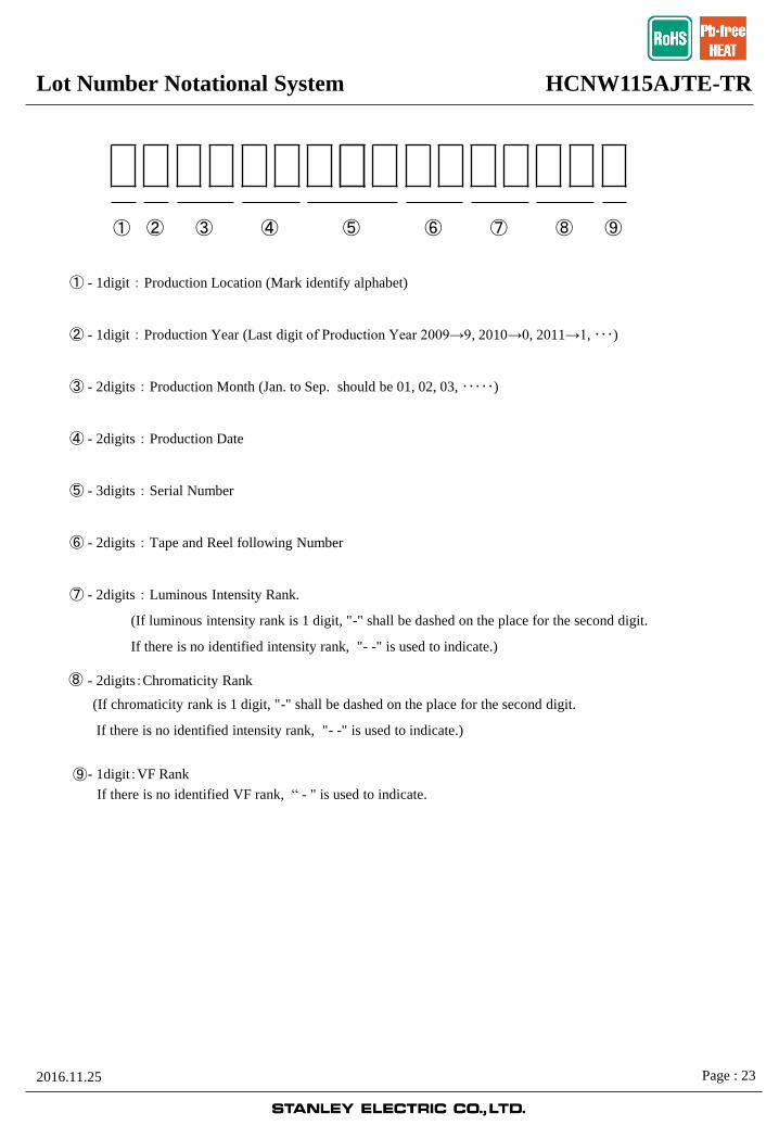
HCNW115AJTE-TR Lot Number Notational System
Page : 23
①
② ③ ④ ⑤ ⑥ ⑦ ⑧ ⑨
① - 1digit : Production Location (Mark identify alphabet)
② - 1digit : Production Year (Last digit of Production Year 2009→9, 2010→0, 2011→1, ・・・)
③ - 2digits : Production Month (Jan. to Sep. should be 01, 02, 03, ・・・・・)
④ - 2digits : Production Date
⑤ - 3digits : Serial Number
⑥ - 2digits : Tape and Reel following Number
⑦ - 2digits : Luminous Intensity Rank.
(If luminous intensity rank is 1 digit, "-" shall be dashed on the place for the second digit.
If there is no identified intensity rank, "- -" is used to indicate.)
⑧ - 2digits:Chromaticity Rank
(If chromaticity rank is 1 digit, "-" shall be dashed on the place for the second digit.
If there is no identified intensity rank, "- -" is used to indicate.)
If there is no identified VF rank, “ - " is used to indicate.
⑨ - 1digit:VF Rank
2016.11.25

HCNW115AJTE-TR Correspondence to RoHS・ELV instruction
This product is in compliance with RoHS・ELV.
Prohibition substance and it's criteria value of RoHS・ELV are as follows.
・RoHS instruction …… Refer to following (1)~(6).
・ELV instruction ………. Refer to following (1)~(4).
Substance Group Name Criteria Value
(1) Lead and its compounds 1,000ppm Max
(2) Cadmium and its compounds 100ppm Max
(3) Mercury and its compounds 1,000ppm Max
(4) Hexavalent chromium 1,000ppm Max
(5) PBB 1,000ppm Max
(6) PBDE 1,000ppm Max
Page : 24 2016.11.25
HCNW115AJTE-TR Reliability Testing Result
1. Reliability Testing Result
2. Failure Criteria
Page : 25
6 Thermal Shock CycleTa=-40(15min.)~125(15min.)
※As shown in the fig.1 below1,000cyc 0/18
7 Resistance to Reflow Soldering
Moisture Soak:Jedec Level2
Preheating:150~180 120sec MAX.
Soldering:260 5sec
2times 0/18
4 High Temperature Storage Life Ta=125 3,000hr 0/18
5 Low Temperature Storage Life Ta=-40 1,000hr 0/18
3 High Temperature Humidity Bias Ta=85 Rh=85% Tj=150 IF=1000mA 1,000hr 0/18
2 Low Temperature Operating Life Ta=-40 IF=1,000mA 1,000hr 0/18
No. Test Item Test Condition Duration Failure
1 High Temperature Operating Life Tj=150 IF=1,000mA 5,500hr 0/18
Ta
30min / Cycle
〈 fig.1 Thermal Shock Cycle Condition 〉
15min
15min 125
-40
Chromaticity
Forward Voltage
Item
Luminous Intensity
Symbol Conditions Acceptance Criteria
IV
IF=1,000mA
Ta=25
Initial Value × 0.8 <Testing MIN. Value & Initial Value × 1.2
≦ Testing MAX. Value
Cx, CyIF=1,000mA
Ta=25Initial Value - 0.02 < Measured Value < Initial Value + 0.02
VF
IF=1,000mA
Ta=25Initial Value × 0.9 < Measured Value < Initial Value × 1.1
Appearance - - Notable discoloration, deformation and crack
2016.11.25

HCNW115AJTE-TR
Special Notice to Customers Using the Products and
Technical Information Shown in This Data Sheet
1) The technical information shown in the data sheets are limited to the typical characteristics and circuit
examples of the referenced products. It does not constitute the warranting of industrial property nor the
granting of any license.
2) For the purpose of product improvement, the specifications, characteristics and technical data described in
the data sheets are subject to change without prior notice. Therefore it is recommended that the most
updated specifications be used in your design.
3) When using the products described in the data sheets, please adhere to the maximum ratings for operating
voltage, heat dissipation characteristics, and other precautions for use. We are not responsible for any
damage which may occur if these specifications are exceeded.
4) The products that have been described to this catalog are manufactured so that they will be used for the
electrical instrument of the benchmark (OA equipment, telecommunications equipment, AV machine, home
appliance and measuring instrument).
The application of aircrafts, space borne application, transportation equipment, medical equipment and nuclear
power control equipment, etc. needs a high reliability and safety, and the breakdown and the wrong operation might
influence the life or the human body. Please consult us beforehand if you plan to use our product for the usages of
aircrafts, space borne application, transportation equipment, medical equipment and nuclear power control
equipment, etc. except OA equipment, telecommunications equipment, AV machine, home appliance and
measuring instrument.
5) In order to export the products or technologies described in this data sheet which are under the
“Foreign Exchange and Foreign Trade Control Law,” it is necessary to first obtain an export permit from the
Japanese government.
6) No part of this data sheet may be reprinted or reproduced without prior written permission from Stanley
Electric Co., Ltd.
7) The most updated edition of this data sheet can be obtained from the address below:
http://www.stanley-components.com/en/
Page : 26 2016.11.25