stag pp39 maintenance manual - freematthieu.benoit.free.fr/stag/pp39/stagpp39servicemanual...pp39...
TRANSCRIPT

Stag Microsystems Ltd Martinfield Welwyn Garden City Herts AL7 1 JT United Kingdom
Tel: (0707) 332148 Fax: (0707) 371503
PP39
MAINTENANCE
MANUAL
Stag Microsystems, lnc 1600 Wyatt Drive Santa Clara, CA 95054 USA
Tel: (408) 988-1118 Fax: (408) 988-1232
803 1083 Rev.2

R E P L Y C A R D
In keeping with our Company policy of continuous enhancement this manual will be under constant review and will be updated when required. In order that the updated vers ions are addessed correctly could the folloiwng manual registration form be completed and returned for the attention of the Service Mana ger, Sta g Electronic Designs Ltd.
QUESTIONAIRE
User ' s Name . . • . . . . • . . • . . . . . . . . . . . . . . • . . . . . . . . . . . . . . . . • . • . . . . • . . . • · · · • · • • •
Title . . . . . . . . . . . . . . . . . . . . . . . . . . . . . . . . . . . . . . . . . . . . . . . . . . . . . . . . . . . . . . . . . . . .
Company
Address
. . . . . . . . . . . . . . . . . . . . . . . . . . . . . . . . . . . . . . . . . . . . . . . . . . . . . . . . . . . . . . . . . .
. . . . . . . . . . . . . . . . . . . . . . . . . . . . . . . . . . . . . . . . . . . . . . . . . . . . . . . . . . . . . . . . . .
. . . . . . . . . . . . . . . . . . . . . . . . . . . . . . . . . . . . . . . . . . . . . . . . . . . . . . . . . . . . . . . . . . . . . . . . . .
. . . . . . . . . . . . . . . . . . . . . . . . . . . . . . . . . . . . . . . . . . . . . . . . . . . . . . . . . . . . . . . . . . . . . . . . . .
Tel ephone . . . . . . . . . . . . . . . . . . . . . . . . . . . . . . Telex . . . . . . . . . . . . . . . . . . . . . . . . . . . .
Fax No . . . . . . . . . . . • . . . . . • . . . . . . . . . . . . . . . . . . . . . . . . . . . . . . . . . . . . . . . . . . . . . . . . . .
Type of ma chine t o which th e ma nual applies . • . • . . . . • • . . • • . • . . . . . . . . . . • . • • •
Ser i al n liTlbe r ............................................................ .
--------------------------------------------------------------------------------
ERROR DETECTION
This maint enance man ual is suppl i ed a s an enhancem ent to Stags co-ordinated internati onal team effort.
Therefore, should any errors be detect ed, we would be gr atef ul if you would contact us as soon as possible as to th e natur e of the mi st ake . Li kewi se if you would like to see i mprovem ents by adding y our own ideas or modi fi cations, then pl ease do not hesitate to contact us at our Head Office in Welwyn Garden City.

PP39 Maintenance Manual
Using this manual
Th is manual consists of eight sect i ons ; each sect ion covers a spec i fic requi rement that a Serv ice Engi neer may, at some time, need to know . Th is manual assumes th at the Service Engi neer i s famil iar with th e operat ing proced ures of the PP39 MOS Programmer, as detailed i n th e Operati ng Instruction Manual .
This manual i s, wh er ever possi bl e, laid out i n easy to follow proced ur es . The perf ormance ch eck section provides a means of proving the correct funct i onal ity of a un it pr ior to de spatch to a customer . Th e calibration procedur e sect ion ena bl es a 'know n good unit' to b e cal ibrated . Th e ma int enance procedur e sect i on consists of a series of t ests ena bl ing fault isol ation with in a fail ed unit .
Test Equipment Required
1. Oscil l oscope eg Tektroni c 2445 2. Digit al Multi-meter eg D at a Pr eci s ion 2480R 3. 39M1 00 Mod ul e 4. 3 9M200 Modul e 5. Means of t esti ng RS232C eg Another PP3 9 .
0-1

CONTENTS
Section 1.0 Technical Description
1 . 1 Block Di ag ram 1 .2 Processor 1 .3 Cl ock G enera tor 1 .4 Decodi ng 1 . 5 DRAM 1 .6 Memory 1 .7 EEPROM 1.8 Di spl ay 1.9 RS232 Int e rf ac e 1 . 1 0 Di spl ay/Keyboa rd Control 1 . 11 LED/Analog ue Control 1 . 1 2 Add ress/Da t a Pin Drives 1 . 1 3 Clamp s Vcc, VP24, VP1 and Ccmponen t s 1 . 1 4 Pull Up Tr ansi s tor 1 . 1 5 Pull Down Transi s t ors 1 . 1 6 Power Up
Sec tion 2.0 Performance Check
2 . 1 Check Sof tware 2 .2 Chec k Cali bration 2 . 3 Check Key board 2.4 Check LED's 2.5 Ch eck Di spl ay 2 . 6 Check EEPROM 2.7 Ch eck DRAM 2 . 8 Check RS232C 2.9 Ch eck Operati on of ZIF Sock e t s 2.1 0 Check Check Prog ramming Capability
Section 3.0 Calibration Procedure
3 . 1 Current Source Cali bration 3.2 Volt ag e Clamp Cali bra tion
Section 4. 0 Mainte nance Procedure
4.1 Test Mode 4 .2 Test Disp l ay 4 .3 Checksurn System PROM 4. 4 Display EEPROM TYpe 4.5 Test DAC' s 4 .6 T est OV Clamp s 4.7 Test Cur rent Gen r ators 4.8 Te st Ad dress Lines 4.9 DRAM Test 4 . 1 0 Tes t Dat a Li nes 4.1 1 Test RS232C 4. 1 2 Tes t EEPROM 4.1 3 Boot EEPROM 4. 14 Checksum Mod ule EPROM 4 .1 5 Calibrate 4 . 16 Access Time Cali bration
0·2-

Section 5.0 Parts List
5 . 1 Ordering Informati on 5 .2 Componen t Li st s 5 .2 . 1 Mai n boa rd 1 00-002 1 5 .2 .2 Power Supply 1 00-0031 5 .3 ! tan s Li st s 5 . 3 . 1 P P 39 Assanbly 1 00-0000 5 . 3 . 2 P P39 Cover Moul di ng Assy 1 00-0003 5 .3 . 3 P P 39 Mai nboa rd 1 00-002 1 5 . 3 . 4 P P3 9 Base Assy 1 00-0002 5 . 3 . 5 P P39 Heat si nk ( 8 TRS ) 1 00-0 0 1 5 5 . 3 .6 P P 39 Heatsi nk ( 3 TRS ) 1 00-00 1 6 5 .3 . 7 P P 39 C abl eform Assy 1 00-00 1 4 5 . 3 . 8 P P39 PSU Boa rd 1 00-003 1
Section 6.0 Component Location
6 . 1 Mai nboard 1 00-002 1 6 .2 PSU Board 1 00-003 1
Section 1.0 Circuit Diagrams
7 . 1 P P 3 9 Mai nboa rd 1 00-002 1 7 .2 P P 39 PSU Boa rd 1 00-003 1 7 .3 P P 39 Mainboard (281 6) 1 00-002 1
Section 8.0 Module
8 . 1 3 9M 1 00 8 . 1 • 1 Componen t Li s t 8 . 1 . 2 !tan s Li st 8 . 1 . 3 Ci rcuit Di ag ram 8 . 2 39M200
0-3

1 .0 Technical Description
This section shoul d be re ad with refe rence to the ill ustrations and ci rc uit di agrams in this ma n ual . It des cri bes the o peration of the P P3 9 MOS P rogr ammer .
1 . 1 Block Diagram
PP39 Main Board
Thi s board provides the following functi onal circuit bl ocks which are subseq ue ntly r eferred t o by th ei r block names:
Function
P roc essor
All clock and timing p uls es
Loc al DRA M storag e
EPROM and s c r a tch-pad memory
EEPROM mem ory
Decoding for this board, mod ul e, and RAM ex t ension, pl us DRA M ref reshing
RS232 Interfac e
Alph anumeric di spl ay and d riv ing el ec t ronic s
Pe ri pheral int erface for devic e d a t a pin drivers and displ ay/key board con trol .
Pe ri phe ral int erface f or LEDs and a nal og ue ele c t ro ni c s con t rol
Pe r iphe ral int erfaces for devi c e add ress/d a t a pins
5 t o 28 V prog rammabl e v ol t ag e clamps
Voltage clamp ov erc urrent d e t ec t or
High vol tag e c ur rent suppli es
5V p ull up s and OV cl amping
Power Up rese t
1-1
Block Name
Z80
Cl oc k Genera tor
DRAM
Memory
EEPROM
Dec oding / DRAM r efresh
RS232 In terfa c e
Di spl ay
Decodi ng/DRAM control
LEDs /A nalogue control
Addr es s/d a t a pin d rivers
Cl amp Vc c Cl amp VP24 Clamp VP1
Canpara t or
Pull up t r ansi s t ors
P ull dow n t r an sis t ors

1 .2 Processor
The Z80 i s an 8 b it processor wh ich can address 64K bytes of memory dire ctly . It is dr iven by a 2MHz clock and may r un softw are resident on the same board or in the module .
In put
E /IRQ / NMI /RES
From
cloc k ge ne rator RS232 interfac e comparator pawer-up
Output Purpose
/ RD /WR /MRW
/RFSH A- bus D-b us
all processor timing I/0 t ransfer inter rupt hardware fa ult interrupt reset process or
processor re ading dat a process or wr it ing dat a indicates val id address on address b us next /M RW for refresh addres s li nes bi-directional data
1 . 3 Clock Generator
1 . 4
The cryst al oscillat or provides a 16MHz sq uare wav e whi ch i s div ided immedi a tely to 4MHz and used for clocking of th e J-K flip- flops . Subsidia ry outp ut s p rovide all sys tem timing incl ud ing DRAM a c cess and re freshing .
In put From Output Purpose
PHI 1 6MHz Xt al all ti ming from thi s MRW Decod ing DRAM a ccess and refresh DAM Decoding DRAM decode
E 2MHz sys tem clock Q quadr ature of E CMUX DRAM address mult i plex /RAS DRAM row select /CA DRAM column select Q2 UART clock
Decoding
Any device on the Z80 dat a bu s ( memory chip, DRAM, PIA LSI de vice etc) receive s a sele ct s ign al when the Z80 w ishe s to access it for a dat a t r ansfer . These select signal s are obtained by compa ring the state of the address bus wi th the pattern all ocate d for e ach dev ice .
In addition certa in m i scallane ou s l og ic fun ct i ons are als o pe rformed .
All these f unct i ons are made by the use of a combinati on of TTL decode rs and FPLA' s . Refer t o ap pendix 1 fo r instruct ion on reading FPLA tables .
Input From Output Purpose
1-2

1 . 5 D RAM
1 . 6
Th e on- board DRAM co nsists of 6�K bytes for holding PROM data . Th i s i s constructed from eight 6�K x 1 DRAM s banked into bloc ks of 1 6K byte s .
Input From Output Purpose
A-b u s Z80 address D RAM wi th in selec ted ba nk
D-b us Z80 bi-di recti onal data RBD Address D at a Drive r selec t DRAM bank RB1 Address Dat a Drive r selec t DRAM bank / RAS Cl ock Gene rator DRAM array row sel ect /CAS D ecod i ng DRAM a rray column sel ect / IM E Decoding D RAM array w rite enable
Memory
The mainf ram e EPROM co nt ai n s the pow er u p i nit i ali sing softwa re, keyboard, displ ay and te st softw are.
Th e scratchpad RAM provide s 2K bytes o f worki ng RAM for t em porary st orage .
Input From Output Purpose
/ RD Z80 processor rea ding IWR zoo pr ocessor writ ing / SPAD Decod ing sel ect s cr atch- pa d RAM /PROM De coding select mainframe EPROM D-b us Z80 bi-di rectional data A-bus zoo address lines
1 .7 EEP ROH
Th e EEPROM i s used to sav e m achi ne p a ramete rs, built up using cert a in 'SET' function s, aft e r th e power h as bee n r emoved . The init i al isati on softw a r e co pies the EEPROM i nto th e scratch- pa d RAM at p ower u p .
On earl ier boa rds th e EEPROM w as a 2 817 requi r ing addit i onal electroni cs fo r it s operation . On later boards a 2 816A typ e EEPROM was f it ted wh ich n eeds no addi tional electron i cs .
Input From Ou tput
D-b us A-bus / DR /WR lEE
EPRM
For b oth EEP ROMs
Z80 zao zao Z80 D ecoding
Addit i o nally for 2 817
RIBU Rffi 3
/-3
Purpose
bi-di re ctional data address lines proce ssor re ading proce ssor w r i ting s el ec t EEPROM
indicates s uccessf ul w r ite 2 1 V req ui red to write to EEPROM t urn s on 2 1 V to EEPROM

1. 8 D isplay
This co nsi sts of a 1 6 ch ar acte r alph a nume r ic vacuum flour escent di spl ay dri ven by a mul tiplexi ng di splay con trol l e r . Con trol and data w ords a re w ri t ten to th e controller ser i ally . The neg a ti ve vol tage s required t o dr ive the d is pl ay are de r ive d fr om a de to de conve rter (IC3).
Input From
RSD DAD CLO
Di spl ay/keyboard control Dis pl ay/keyboa rd control Di splay/keyboa rd co ntrol
Displ ay PSU (IC3)
1 • 9 RS232 Interface
Output Purpose
P i n 3 Pin 4 Pin 6
reset dis pl ay controller seri al dat a inp ut cl ocks seri al data
approx -25V de app rox 2V rms -20V de approx 2V rms -20V de
This uses a n LSI universal asynch ronou s receiver/tr ansm itter (UART) to convert pa r allel 8-bit data to seri al form . Th e UART i s buffe red and connected to the 25-way fem ale connect or.
Input From Ou tp ut P urpose
02 cl ock ge nera tor UART reg ist er sele ctio n A1 , AO zao bi-di re ctio nal data D-b us z8o da ta direction control RIW decoding intern al t iming of UART /URT decod i ng UART select sign al /RES power up UART re set
/ IRQ I/0 interru pt to zao
/ RXD 25 way conn pin 3 CTS 25 way conn pin 5 DSR 25 way conn pin 6 DCD 25 way conn pin 8
TXD p in 2 RTS p i n 4 DTR p i n 20

1 .10 Display/Keyboard Control
Th e di spl ay i s co ntrolled by send ing se r i al d at a t o the di spl ay co n trolle r ove r ' DAD' synch ron ised by a clock ing s ig n al o n ' CLD' .
Th e keybo a rd con si s t s o f a m atr ix of columns and rows where p ressing a key w ill make a connect ion between a part ic ul a r row and column l ine . The PIA o u tp ut s a pa ttern to the col umn s and reads back the status of the row s . From th i s, the proces sor c an calc ul a t e th e key pressed .
P ROTA o f the PIA connect s onto th e RD-b us as de scr ibed i n th e Addr ess/Da t a Pi n Drive r sect ion .
Th e inp uts t o a nd o u tp ut s from th i s block are define d i n th e following tabl e:
Input
AO, A1 D-b us PORT4 R ES Pi ns 1 4- 1 7
From Output
Z80 zao decodi ng power- up CONN K
Pi n 1 3 Pin 1 8-25 DAD CLD RSD RD-bus
Purpose
PIA reg i s te r selec tio n b i-d i rect ional d a ta selec t PIA reset PIA reg i ste rs to keybo a rd row li nes
to key board colum n l ine t o keyboa rd colum n l ine s ser i al dat a to d i spl ay con t roller clock ing d a t a on DAD di splay con t rolle r re se t bi-d irec t ion d a t a t o dev ice data p in s
1.11 LED/Analogue Control
Thi s PIA i s m a i nly used for control of the analogue driv ing electronics ie p ull up transistors, clamp s and pull down transistors . Addi t ional func t ion s are incl uded i n the table below:
Input From Output Purpose
AO, A1 Z80 PIA regi ster selec t ion D-bus Z80 b i-direc tional dat a PORT1 decodi ng sel ec t PIA RES pow er up re set PIA r eg ist ers R/00 EEPROM i ndica tes suc cessful EEPROM
w ri te * CTS RS23 2 interface RS232 handsh ake signal
*
I..2 8 L24 R24 R28 EPRM CON
EIXi DX1 - DX4
Y 1 -Y7
mod ul e LED's mod ule LED' s mod ul e LED' s mod ul e LED' s cont rol s EEPROM h i voltage * turns o n clamp s Vc c, VP1 and VP24 access t i me co ntrol con trols pull down transi stors a, b, c and d cont rols all pull up trans ist ors
signal only appl i es t o board s fitted w i th 2 817 EEPROM.
1-5

1.12 Address/Data Pin Drivers
These two PIA' s a re used mainly for d riving d evice address pins and d riving / sensing d evice data pin s . Addi tional fun c tions are incl uded in th e tabl e b elow:
Input From
AO, A1 zao D-bus Z80 PORT2 d ecoding PORT3 d ecoding RES pow er-up
Outp ut
PA-b us QA9, 1 1 ,
LD-bus
RD-bus
RB -bus WAGL WAGR BLP
1 3
Purpose
PIA regi ste r sel ec tion bi-di rec tion al data selec t PIA sele ct P IA rese t PIA reg i s ters
drive d evi ce add ress pins control s pull down tran si stors e, f and g bi-d i rec ti onal d a ta to dev ice data pins bi-di rectional d a ta to dev ice data p in s selec t DRAM ban k con trol 1 0K p ull up s on LO-bus con trol 1 0K pull ups on RD-bus con trol blee per
1.13 Clamps Vcc, VP24, VP1 and comparator
As all th ree DAC's are practi cally ide ntic al only one ne eds to be des c ribed, clamp Vcc .
The DA C l a tch es on 8-bi t v al ue wri t ten to i t by th e processor and p roduces a nega ti v e vol tag e pro portion al to i t at pi n 1 6 of the DAC . An error v ol tage a t pin 5 of th e o p amp i s ampl i fi ed and used to con trol the c urren t sin k TR9 . Thi s con trol s whe ther c urrent is flowing i n to C30 from TR 1 1 or out of C30 i n to TR9 and hence th e vol tage across C30 . Th e cl amp tran si stor TR1 3 prov i des current ga in and sets th e cl am p output vol tag e .
Th e v ol tage a t th e colle ct or of TR1 3 is de termin ed by R2 4 an d is used by th e compa rator to de tect an over curren t fa ul t which then genera tes an/ NMI .
Th e inp uts to and outputs from thi s block a re defin ed i n the followi ng tabl e:
Input
D-b us IWR /DAC 1 /DAC2 /DAC3
From
Z80 ZBO decoding d ecoding decodi ng
Output Purpose
bi-di rec ti onal d a ta processor w ri ting select DAC 1 sel ect DAC2 sel ec t DAC3
VCC clamps coll ector of p ull up tran sistor s
VP24 clamps coll ector of pull up transis tors
VP1 clamps coll ector of pull up t r ansi st ors
/ NMI i nd i cate to Z80 hardware faul t

1.14 Pull Up Transistors
Th e function of th ese i s to take a dev ice p in to a h igh vol tage . Pull up transistors associa ted wi th outp uts b and g are connected to the +1 5V rail as opposed to +32V used on outputs a, c, d, e and f .
Th e i np uts t o and output s from thi s block a re defi ned i n th e follow ing table:
Input
Y 1 -Y7
From
LED/anal ogue con trol
1.15 Pull Down Transistors
Outp ut Purpose
con trol of pull up transist ors
a to g high v ol tage p in d r ivers
These enable outputs a to g to be clamped to OV. These outputs go di rectly to th e modul e .
Th e inp uts t o and output s from thi s block a r e d ef ined i n the following table:
Input
DX1-DX3
QA9, 11,
1 . 1 6 Power Up
13
From
LED/anal ogue control
Addres s/da ta pi n d r ivers
Output Purpose
con trol of pull dow n trans istors
co ntrol of pull dow n tran sistors
a to g high vol tag e pi n drivers
Applicati on of mai ns powe r produces a long pul se on the / RES and R ES l ine s wh i ch i ni tiali ses the Z80, UART and por ts .
The inp ut s to and outputs from thi s block a re d efined in the followi ng tabl e:
Input From
appl ica ti o n of power
I 12V Supply
Output
RES / RES
Purpose
cha rges C22 th rough R1 0
high power-on p ulse low pow er-on pulse
Provides a regulated I 12V supply f or the RS232 interface and certain of the pull up transi s tors .
1-7

2.0 Performance Check
2 . 1
2.1 . 1
2.1 .2
This sectio n of the man ual des cribes a me thod of checki ng tha t a PP39 MOS Programme r i s functioning corre c tly . These tests shoul d be ca rri ed out p rior to despa tch to a cus tome r . Howev er, these p roced ure s shoul d o nly be used as a fi nal te s t and, should a ny tes t fai l, pl ease refe r to se c tio n 4 - Mai ntenance Proce dures .
Check Software
Check Software Revision
Remov e any mod ule for PP39 P�ER ON Di splay wil l read MODULE? Pr ess SET Key Press 6 key s Di splay will read P P39 Iss XX Where xx is th e revision of the main frame s oftware
Ens ure tha t thi s i s th e appro pria te revi sio n .
P�ER OFF
Insert mod ule and repe at proced ure above to ch ec k r ev i sion of module .
Di spl ay read "Module KxOO XX" Where x i s th e module numb er Re pe a t for any o the r mod ules
Check Software Checksums
Access Test Mod e Key sequence SET, HIDDEN KEY (Between LOAD and EDIT) A, B, A Display should rea d TEST ENTER - -
Sel ect test 05
The checksum of the sy s tem eprom will b e displayed - Ensur e this agrees wi th the issue.
Press EXIT Di splay will read TEST ENTER Select test 85
The ch ecksum of th e mod ul e eprom will be di spl ayed - Ensure thi s agrees with the issue.
Rep eated f or any other mod ul es
2.·1

2.2 Check Calibration
Th e na tu r e of the ci rc ui try of th e PP3 9, requi res th e PP39 t o b e di smantled for Calibration Ch ecking; to do this proceed a s f olla.�s:-
1 . Dis connect unit from ma ins s upply .
2 . Remove from base of un i t th e three sc r ews nearest the front, which sec ur e th e bas e to th e cover mould ing .
3 . Remove f rom the rear pa nel th e two sc rew s nearest the top c orners .
4 . Ca refully sepa rat e the c over mouldi ng from th e base assem bly .
NOTE 1: The power supply is mounted on the base and is connected to the mainboard via a cableloom assembly.
5 . Plac e th e uni t s uch tha t th e tw o halves a r e still el ect rically connec ted by the c abl el oom assembly a nd ac c ess can be made of the p c b' s .
6 . Reconnect to swi tchabl e mai ns s upply and i nser t 3 9M1 00 then sw i tch on .
7. Th e following proc ed ure check s th e correc t c al ibr a ti on of th e c urrent s ourc e of the PP3 9 .
P ress SET key P r ess HIDDEN key - betw een LOAD and EDIT keys Pr ess A k ey Press B key Press A key - Displ ay w ill read TEST ENTER - -Selec t t est 86
The di splay w ill now be CALIB RATE
Meas ur e the v ol tages ac ross R88 th en R84 and ch ec k for 2.70V + or - 0.1V
8 . Th e follow i ng proc edure ch ecks the correc t vol tage cal ib r ation of th e cl amps .
Chec k the vol tag es a nd ensur e th ey conform to th e tabl e below:-
Test Point
D9 Anode (TP 1 ) 0 1 5 Anod e (TP2) 0 1 6 Anod e ( TP3)
Measur ed Voltage
1 2 .5 V 1 2 . 5 V 6 . 00V
Tolerance
+ or - 0 . 0 1 V + or - 0 .0 1 V +or - 0 . 01V
Note 1: Use negative end of ca pacitor C22 for OV reference of voltmeter.
2.-2

2 .3 Check Keyboard
Ranove Modul e PCMER ON Displ ay will read MODULE? Press each key i n turn and ensure th e ho rn will sound a t each key p r ess
This p roves th e contac t s of all th e k ey s o f th e mem brane panel.
However, to p rove th e PP39 ca n int e r pr et th e c orrec t keys, i t i s ad visa ble t o power off, insert a module, power on, and check the unit re sponds correctly as each key i s pressed . ( Re fer to Operating Instruc ti on Manual ).
2 . 4 Check LED's
The p roc edure below desc rib es th e method of ch ec king correc t LED control for the 3 9M1 00. A simila r t echniq ue sho uld be used for any o ther av a il a bl e mod ul e.
PP39/39H100 LED's
In stall 3 9M1 00
Power On
Press SET key Press 0 k ey Pr es s DOWN ARROW key ONCE Press EXIT key Press SET k ey Press 3 key Press DOWN ARROW key or UP A RROW k ey Displ ay shows MODE 8 BIT Press EXIT k ey
The d i splay should r ead AMD 2716 M8 and th e Two LEDs in rel a tion to th e 24 pin devic e on each soc ke t, sho uld illumina te only.
Press SET key Press 0 key P r ess RIGHT ARROW key SIX TIMES Press EXIT k ey
The di spl ay should now need AHD 27128 M8 and th e Two LEDs in r el a tion to th e 28 pin d evic e, o n each socke t, sho uld illumina te only.
Press SET k ey Pr ess 0 k ey Press LEFT ARROW k ey THREE TIMES Press EXIT key
Th e horn should sound and th e d i spl ay w ill read RAM EXCEEDED, th en the LED for right socket will EXTINGUISH only and the display will read AHD 27512 M8.
Z-3

2 .5 Check Display
Access test mode (keysequence is SET, HIDDEN KEY (between LOAD a nd EDIT), A, B, A)
Display will read TEST ENTER - -Select test 00 Display should read ••••••••••••••••
Press EXIT Select test 01 Display should read 0000000000000000 Press EXIT Select test 02 Display should scroll a * from right to left Press EXIT Select test 03 Display should scroll a 0 from right to left Press EXIT
2 .6 Check EEPROM
Access test mode (key sequence SET, HIDDEN KEY (between LOAD and EDIT), A, B, A)
Display will read TEST ENTER - -Select test OD Display will read EET ( EEPROM Test) After approximately 25 seconds display Display will read PASS Press EXIT Display will read TEST ENTER - -Select test 84 (Module must be inserted) Display will read EEPROM BOOT then return to TEST ENTER - -
This is essential to execute this boot after an EEPROM TEST to re-configure valid EEPROM data.
2 .7 Check DRAM
Access test mode Select test OB Display should read DRA and af ter a period of time PASS Press EXIT
2. 8 Check RS232C
The UART can qui ckly be checked by a selftest.
LINK PIN 2 to PIN 3 of RS232C connector Access TEST MODE Select test OE Display should read IFA then PASS
2.-4

2 . 9 Check Operation of ZIF Sockets
For this test two EPROMs are required1 x 2ij pin and 1 x 28 pin both with known checksums.
Using a 2� pin programmed EPROM (with known C/SUM, eg 2716) proceed as follows:-
Press SET 0 Using UP and DOWN cursor keys locate manufacturer of device Using LEFT and RIGHT cursor keys locate device type Insert device in to SKT 1 Press LOAD key Display should read XX.XX CSUH (where XXXX = checksum of device) Place same device in SKT 2 Press LOAD key Display should read CSUH XXXX (where XXXX = crrecks urn of device) Press Cl SUH key Display should read XXXX CSUH XXXX and both checksums should be the same Remove 2� pin device and repeat for 28 pin EPROHs
2 .10 Check Programming Capability
Using the 28 pin programmed EPROM (with known C/SUH, eg 27128) proceed as follows:-
Press SET 0 Using U P and DOWN cursor keys locate manufacturer of device Using LEFT and RIGHT cursor keys locate device type Insert master dev ice in to SKT 1 Press LOAD key Display will read XXXX CSUH Remove dev ice from socke t and place in SKT 2 Press LOAD key Display will read CSUH XXXX Remove master from socket 2 Press C/SUH key Display will read XXXX CSUH XXXX Insert two suitable empty devices into the socke ts Press EHPTY key Display will read PASS EHPTY PASS Press PROGRAM key Display w ill read PASS BIT TEST PASS Then change to PROGRAMMING XX where xx is a counter up to 40 in Hex (If 27128) Then change to PASS VERIFY PASS
2.-5

3 . 0 Calibration Procedure
T o correctly calibrate the PP39 proceed as follows:-
Section 2.2 describes access to the c ali b ratio n poi nts and explains how to check c ali b r a ti on.
With reference to this section and th e tabl e below the c ali b r ation can b e adjusted.
3.1 Current Source Calibration
Voltage Ac ross R88 = 2.7V + or - 0.01V Adj us t RV1 on PSU
3.2 Voltage Clamp Calibration
Test Point Measured Voltage Tolerance
0 9 Anode (TP 1 ) 1 2.5V + or - 0 . 01V 015 Anode (TP2) 12 . 5V + or - 0 . 01V 0 1 6 Anode (TP3) 6.00V + or - 0 . 01V
VR1 VR3 VR2
on Main
3-/
Adjust
Board
4 . 0 Maintenance Procedure
To aid the Service Engineer the PP39 has several test rou tines, which allow various parts of the circuitry to be more easily tested.
4. 1 Test Mode
To gain access to the tes t routines it is necessary to enter a coded sequence of key presses. This is arranged like this to prevent a customer accidently ex ecu tin g a tes t when a device is fitted into a ZIF socket.
The following instructions permit access to the test mode:-
Press SET key Press HIDDEN key Press A key Press B key Press A key
The display will now read ENTER TEST - -
The tests available can be split into two catagories:-
1 . Mainframe test- test numbers 00 to 7F. 2. Module execute tests- test numbe r 80 toFF.
Note: Whilst in test mode the LIST RAM, EDIT RAM functions actually permit access to the 'REAL' address map of the PP39 ie. control latches etc can be written/read directly from the keyboard.
4.2 Test Display
There are four display pa tterns , this tes t continuously write to the display controller the screen pattern of instructions, thus if an incorrect display is present it is possible to fault find using an oscilloscope etc.
Test 00 - Displays a * in all 16 display positions Test 01 - Display a 0 in all 16 display positions Test 02 - Displays a single * and scrolls this from right to left Test 03 - Display a single 0 and scrolls this from right to left.
4-1

4 .3 Display EEPROK Type
Test 04 EET
Th e P P3 9 was originally designed t o em pty a 281 7 type of EEP ROM, however, th i s has now be en cha nged t o ty pe 2 81 6 . The later dev ice can be p rogrammed more q uickly, tha n the origional. Hardw a re modif ica tions have bee n made to the EEPROM ci rcui t ry to suit th e 2 817 EEPROM .
However, t o sim pl ifY s oftw are iss ues ( i e only one EPROM i nd ependa nt of ty pe of EEPROM ) , th e programming of th e EPROM defa ul t s t o the l onge r programming cycl e, unl ess it reads from the EEPROM that i t i s ty pe 2 81 6 a nd i n this c ase it runs th e fast er algorithm .
T est 0 4 a t tempts t o w ri t e t o the EEPROM usi ng th e fas ter algorithm and if successf ully s tored, the di spl ay show s 2816 o therwise it show s 2817.
Af ter this t es t has bee n exec uted th e fas te r algor i thms w il l always b e used ( i f a p pl ic abl e ) .
4 . 4 Checksum System PROM
Test 05 SYS CSUM
Th is test checksums a nd dis pl ays the sys tem EPROM .
4-2..

4 . 5 Test DAC 's (Dig ital to Analogue Convertors)
Test 06 Ramping DACs
This test ramps all the DAC's in a continued loop.
Set oscilloscope to 1ms/Div; 2 volts/Div check the waveforms, at pin 1 6 of IC's 42, 4 4 an 46, agree to that shown below:-
Test 07 B it Walk DAC's
Thi s test writes the pattern 01, 02, 0 4, 0 8, 10, 2 0, 40, 80 continuously to the DAC's.
Set oscilloscope to 50mS/Div, 2 volts/Div and compare the waveforms at pin 1 6 of IC's 4 2, 4 4 and 46 with that shown below:-
I
I I
33�
Sv

4.6 Test OV Clamps
Test 08 OV Clamp Walk
Thi s test the seq ue nce s of the O V clamps, set th e osci l l oscope to 50mS/Di v, 1 Volt/Di v and compa re the w av eforms, of pin 14, IC33 ( DX1) ; i n 15 IC33 ( DX2) , and pin 16 IC33 (DX3), with th at show n below:-
1-
Also check w av eform a t p i n 1 7 IC33 (DX4) and compar e wi th that shown below : -
Pin's 1 2 of IC34 (QA13), 15 (QA9) and 17 (QA11) with tha t shown below:-
'• '• ••
170,...5
4-4-
Z.Sv
l.Sv

4 .7 Test Current Generators
Test 09 Current Gen Walk
Set oscilloscope t o 50mS/Div, 1 vol t/Div and comp a re the w avef orm b elow to tha t measured on pins 1 0 ( Y 1 ) , 1 9 ( Y2 ) , 2 0 ( Y3), 2 1 (Y4), 22 ( Y5 ) , 23 ( Y6) and 2 4 (Y7) of I C33 .
4 . 8 Test Address Lines
200pS
Test OA Bit Walk Address
This t est w rit es a p a ttern to b o th th e high addres s and th e low address lines a t th e same time; s e t oscilloscope to 50mSec/Div, 1 Vol t/Div and compa re th e associ a ted meas urement wi th those shown i n the di ag rams ov e rl e af:-
4-5
3.8v

IC34 pins 1 0 ( pa 1 5 ) , 25 ( pa7 )
4v
IC34 pins 1 5 ( Qa 9) , 17 (Qa11 )
- -
IC34 pin 1 2 ( Qa 1 3 )
- -
2..SV
zso,....s
4-&

IC34 pins 1 1 ( PA1 3 ) , 13 ( PA12), 1 4 ( PA 7 ) , 1 6 (PA8), 1 8 (PAO), 19 ( PAl) , 20 ( PA2), 2 1 (PA3), 22 (PA4), 23 (PA5) a nd 24 (PA6).
4.9 D RAM Test
Test OB DRA
4v
This t est ch ecks th e DRAM by wri ti ng and r eadi ng from the DRAM . If a failure occurs the display will show the failed address the expected result and the actual result. Also at this time the micrprocessor i s con tinuously loo ping at this RAM address.
Exampl e of fail ur es:
004000
Address
00
Exp ected Res ul t
46
Ac tual Res ul t
If the RA M test i s successf ul th e di spl ay will read PASS . A famili ar l oca tion can b e skipped by using the down c ursor k ey at the t est wil l conti nue to th e nex t fail ur e (i f any ).
4.1 0 Test Data Lines
Test QC LDR
This s elftes t w ri t es to and r ead s b ac k th e data pi n d ri vers . Again shoul d a f ail ur e occ ur the displ ay will show b o th th e exp ec t ed and the actual resul t and th e proc essor l oops on this t est eg .
3A > 2A 02 06
0/ P Port I/ P Por t Data Sent Data Rec eiv ed
Pres s the dow n c urs or key to skip through test .
4--7

4 . 1 1 Test RS232C
Test OE IFA
This t est requi res pi ns 2 and 3 of RS232C to b e limi t ed . It pe rf orms a seri e s of tests ch ec ki ng th e Uart parameters . Obviously, thi s t est i s not proof of correct RS232C ope rati on and this must b e checked connected to a syst em . How ever this t est is us ef ul for fault di ag nosi s .
A typical fail ur e result i s show n he r e .
C C - 91 6 B S-1 6
Where C C i s 1 . Control regi s ter 2, Comm and regi s ter 91 i s d a ta of Control regis te r 6B i s da ta of Comm and regi ster S-16 is Sta tus regis ter
The fol l ow ing tables show det ails of these regis te rs .
Note: usi ng th e dow n cu rs or you c a n skip a failure in the test and con tinue to the nex t failures (if any) .
4-8

CONTROL REGISTER
"Cc-91 6B S-16"
STOP BITS
0 = 1 STOP BIT
1 = 2 STOP BITS
1 STOP BIT IF WORD LEr-x;1H 8 BITS & PARITY 1 1/2 STOP BITS IF WORD LENG1H = 5 BITS & NO PARITY
I WORD LENGTH
0 0 8 0 1 7 1 0 6 1 1 5
�ECEIVER CLOCK SOURCE I ... _ ... _ ,...,._... ... -
ID7 1 D61 D5 D4 1 D3 1 D2 D1' DOl 80 40 20 0 8 4 1
I
BAUD RATE GENERATOR
0 0 0 0 16X EXTERNAL CLOCK 0 0 0 1 50 BAUD 0 0 1 0 75 0 0 1 1 109.92 0 1 0 0 1 3 4 .58 0 1 0 1 1 50 0 1 1 0 300 1 1 1 1 600 1 0 0 0 1200 1 0 0 1 1800 1 0 1 0 2400 1 0 1 1 �6 00 1 1 0 0 4800 1 1 0 1 7200 1 1 1 0 �00 1 1 1 1 19200
4-9

COMMAND REGISTER
"cC-91 68 S-1611
1071 061: D5 1� D4 1 D3/ D
80 40 20 10 8 4 D1 DOJ 2 1
I
l PARITY CHECK CONTROLS - - 0 PARITY DISABLED - NO
PARITY BIT GENERATED -NO PARITY BIT RECEIVED
0 0 1 ODD PARITY RECEIVER
AND TRANSMITTER 0 1 1 EVEN PARITY RECEIVER
AND TRANSMITTER 1 0 1 HARK PARITY BIT
TRANSMITTED, PARITY CHECK DISABLED
1 1 1 SPACE PARITY BIT TRANSMITTED, PARITY CHECK DISABLED
' NORHALIECHOHODE FOR RECEIVER I 0 =I NORMAL , 1 =I ECHO (BITS 2 & 3 MUST 11011)
0 0 1 1
DATA TERMINAL READY 0 = DISABLE RECEIVER
AND ALL INTERUPTS
(DTR High) 1 = ENABLE RECEIVER
AND ALL INTERUPTS
(DTR Low)
RECEIVER INTERRUPT ENABLE 0 = IRQ INTERRUPT ENABLED FROM
BIT 3 OF STATUS RffiiSTEH
1 = IRQ INTERRUPT DISABLED
TRANSMITTER CONTROLS
TRANSMIT INTERUPT LEVEL TRANSMITTER
0 DISABLED HIGH OFF 1 ENABLE LOt/ ON 0 DISABLED LOt/ ON 1 DISAB LED LW TRANSMIT
BRK

STATUS REGISTER
" Cc-91 6 B 5-16n
l D7J D6jD5J D4JD3J D2J D1 I DO I STATUS SET BY CLEARED
..__ PARITY ERROR 0 = NO ERROR SELF CLEA RING
1 = ERROR
FRAMIM:J ERROR 0 = NO ERROR SELF CLEARIOO 1 = ERROR
OVER RU N 0 = NO ERROR SEL F CLEARING 1 = ERROR
RECEIVE DATA 0 = NOT FULL REA D RECEIV E R ffi ISTER FU L L 1 = FU L L DATA REG ISTER
TRANSMIT DATA 0 = NOT EMPTY WRITE TRANSMIT REG ISTER EMPTY 1 = EMPTY DATA REDISTER
DCD 0 = DCD = LON NOT RESETTABL E 1 = DCD = H IGH REFLEC1S DCD
STATE
DS R 0 = DSR = LON NOT RES ETTABLE 1 = DS R = HIGH REFLECTS DS R
STATE
IRQ 0 = NO INTERRU PT READ STATUS 1 = INTERRU PT Rffii STER
4-11

4 . 1 2 Test EEPROH
Test OD EET
This t est ch ecks the EEPROM, how ev er should a f ail ur e oc cur this test does not loop (t o preserv e EEPROM life time ) .
A typi cal fail ur e woul d b e: -
2840 BC - FC
Whe n 2 840 i s the faili ng address
BC is the writ ten da ta FC is th e rea d da ta
Th e down curs or k ey conti nues the te st t o the next failur e (if any ) .
4 . 1 3 Boot EEPROH
Test 84
This test 'boots' the modul e fitt ed . modul e oper ation . made .
th e EEPROM with vali d paramet ers appli cabl e to This t est must be exec ut ed for consist ant
Otherwi se a s eri es of s tor e opera tions must be
4 . 1 4 Checksum Module EPROH
Test 85
This t est ch ecksum s the modul e EPROM.
4.15 Calibrate
Test 86
Pl eas e r ef er to cali br at e pr ocedur e
4 . 1 6 Access Time Calibrate
Test 87
Using an oscillos cope s et to 0 . 1 mSI Div, 1 Volt/Div . Adjust RV1 on 39M100 module (only) whilst moni toring modul e test p oi nt 1 and check time p e riod varies from appr ox 0.05mS to 0.55mS.
4-IZ

5 .2 Component Lists
5 .2 . 1 5 .2 .2
Mainboard PCB Power Supply
5-/
1 00-002 1 1 00-003 1

C O M PO N E N T L I S T 1 0 0 - 0 0 2 1 P P 3 9 P CB IS S U E 6
c 1 4 1 2 3 1 0 0 C A P M U LT I LAY ER C E R AM I C 0 . 1 u F 5 0 V c 1 5 1 2 3 1 0 0 C A P M U LT I L AY E R C E R A M I C 0 . 1 u F 5 0 V c 1 6 1 2 3 1 0 0 C A P M U L T I L AY E R C E R AM I C 0 . 1 u F 5 0 V c 1 7 1 2 3 1 0 0 C A P M U L T I L A Y ER C E R A M I C 0 . 1 u F 5 0 V c 1 8 1 2 3 1 0 0 C A P M U L T I L AYER C E R AMI C 0 . 1 u F 5 0 V c 1 9 1 2 3 1 0 0 C A P M U LTI L AY ER C E R A M I C 0. 1 u F 5 0 V c 2 0 1 2 3 1 0 0 C A P M U L T I L AY E R C E R AM I C 0 . 1 u F 5 0 V c 2 1 1 2 3 1 0 0 C A P M U L TI L AY E R C E R A M I C 0. 1 u F 5 0 V c 2 2 1 1 0 043 C A P A L EL E C A X I A L 4 7 u F 1 0 V c 2 3 1 2 3 1 0 0 C A P M U L TI LAY E R C E R A M I C 0 . 1 u F 5 0 V c 2 4 1 2 0 1 04 CA P R ES I N DI P P E D T A N T 1 . 5 u F 3 5 V c 2 5 1 2 3 1 0 0 C A P M U L T I LAY E R C E R A M I C 0 . 1 u F 5 0 V c 27 1 2 3 1 0 0 C A P M U L T I L AY E R C E R A M I C 0 . 1 u F 5 0 V c 2 8 1 2 3 1 0 0 C A P M U LT I L AY E R C E R A M I C 0 . 1 u F 5 0 V c 2 9 1 2 3 47 4 CA P M U LT I LAY E R C E R A M I C 0 . 4 7 u F 5 0 V c 3 0 1 2 3 4 7 4 CA P M U L T I LAY E R C E R A M I C 0 . 47 u F 5 0 V c 3 1 1 2 3 1 0 0 C A P M U LT I LAY E R C E R A M I C 0. 1 u F 5 0 V c 3 2 1 2 3 1 0 0 C A P M U L TI LAY E R C E R A M I C 0 . 1 u F 5 0 V c 3 3 1 2 3 47 4 C A P M U L T I L AY E R C E R A M I C 0 . 47 u F 5 0 V c 3 4 1 2 3 1 0 0 C A P M U L T I L AY E R C E R A M I C 0 . 1 u F 50 V c 3 5 1 2 3 1 0 0 C A P M U L T I LAY E R C E R A M I C 0 . 1 u F 5 0 V c 3 6 1 2 3 1 0 0 C A P MU L T I L AY E R C E R A M I C 0 . 1 u F 5 0 V c 37 1 2 3 1 0 0 C A P M U L T I LAY E R C E R A M I C 0 . 1 u F 5 0 V c 3 8 1 2 3 1 0 0 C A P M U LT I LAY E R C E R A M I C 0 . 1 u F 5 0 V c 3 9 1 2 4 5 6 2 C A P M U L T I L AY E R C E R A M I C 5 6 0 0p F 5 0 V c 4 1 1 2 4 1 0 2 C A P M U L T I LAY E R C E R A M I C 1 0 0 0p F 50 V X 1 3 0 8 0 0 3 C R Y S T A L 1 . 843 2 MH Z M 1 1 0 0 - 0 0 2 2 P P 3 9 P CB M 2 3 0 9 1 6 5 D I S P L AY F I P 1 6 A5 R M 5 4 0 0 0 6 0 S OL D E R P I N D/ S M 6 4 0 0 0 6 0 S OL D E R P I N D/ S M 7 4 0 0 0 6 0 S OL D E R P I N D/ S M 8 4 0 0 0 6 0 S O L D E R P I N D/ S M 9 1 0 0- 0 0 1 4 P P 3 9 CAB L E FO R M A S S Y M 1 7 3 1 8 7 64 E P R O M 27 64 M 2 4 4 0 0 0 6 0 S OL D E R P I N D/ S M 2 5 4 0 0 0 6 0 S OL D E R P I N D/ S M 2 6 4 0 0 0 6 0 S OL D E R P I N D/ S M 2 7 4 0 0 0 6 0 S OL D E R P I N D/ S M 28 4 0 0 0 6 0 S O L D E R P I N D/ S M 29 4 0 0 0 6 0 S OL DE R P I N D/ S M 3 0 4 0 0 0 6 0 S OL D E R P I N D/ S
5-2.

CO M PO N E N T L I S T 1 0 0 - 0 0 21 PP 39 P CB IS S U E 6
R 9 2 R 9 3 R 9 4 R 95 R 96 R 97 R 9 8 R 99 D 1 D 2 D 3 D 5 D 6 D 7 D 8 D 9 D 1 0 D 1 1 D 1 2 D 1 3 D 14 D 15 D 1 6 D 1 7 D 18 D 1 9 D 2 0 D 2 1 D 2 2 D 2 3 D 2 4 D 2 5 D 2 6 D 27 D 2 8 D 2 9 D 3 0 D 3 1 D 3 2 D 3 3 D 3 4 D 35 D 3 6 D 3 7 D 3 8 D 3 9 D 4 0 c 1 c 2 c 3 c 4 c 5 c 6 c 7 c 8 c 9 c 10 c 11 c 12 c 13
1 3 2 1 0 0 1 3 1 6 81 13 1 27 2 1 31 27 2 1 3 1 3 3 3 1 3 5 1 80 1 35 1 8 0 13 5 27 0 2 8 8 1 07 2 8 4 1 4 8 2 8 4 1 4 8 2 8 4 1 4 8 2 8 4 1 4 8 2 8 4 1 4 8 2 8 4 1 4 8 2 8 4 1 4 8 2 8 4 1 4 8 2 8 4 1 4 8 2 8 4 1 4 8 2 8 4 1 4 8 2 8 4 1 4 8 2 8 4 1 4 8 2 8 4 1 4 8 2 8 4 1 4 8 2 8 4 1 4 8 2 8 4 1 4 8 2 8 4 1 4 8 2 8 4 1 4 8 2 8 4 1 4 8 2 8 4 1 4 8 2 8 4 1 4 8 2 8 4 1 4 8 2 8 4 1 4 8 2 8 4 1 4 8 2 8 4 1 4 8 2 8 4 1 4 8 2 8 4 1 4 8 2 8 4 1 4 8 2 8 4 1 4 8 2 8 4 1 4 8 2 8 4 1 4 8 2 8 4 1 48 2 84 1 4 8 2 8 4 1 4 8 2 8 4 1 4 8 2 8 4 1 4 8 2 8 4 1 4 8 110 0 07 110 0 07 12 3 1 0 0 1 1 0 0 4 4 12 3 10 0 1 2 0 1 0 4 12 3 10 0 12 3 1 0 0 120 104 123 011 12 3 0 1 1 12 3 011 123 011
5-3
R E S I S TO R CA R B O N F I L M 0.5W 5$ 10 R R ES I S TO R CA R B O N F I L M 0.25W 5$ 6 80 R R E S I S TO R C A R B O N F I L M 0.25W 5% 2K7 RES I S TO R CA R B O N FIL M 0.25W 5$ 2 K7 R E S I S T O R C A R B O N F I L M 0.25W 5$ 3 3 K R E S I S T O R TH I C K FIL M 0 . 5W 2$ 18 R RES I S TO R TH I C K F I L M 0 . 5 W 2 $ 1 8 R R ESI STO R TH I C K F I L M 0. 5W 2% 27 R DIO DE Z EN E R 1 .3W B Z X 6 1 C 1 5 V D I O D E 1 N 4 1 4 8 D I O D E 1 N 414 8 D I O DE 1 N4 1 4 8 DI ODE 1 N 4 1 4 8 DI O D E 1 N 4 1 4 8 D I O D E 1 N 4 1 4 8 DI ODE 1 N 4 1 4 8 DI O DE 1 N 4 1 4 8 DIO DE 1 N 41 4 8 D I ODE 1 N 4 1 4 8 DIO D E 1 N 41 4 8 DI ODE 1 N41 4 8 D I O D E 1 N4 1 4 8 D I OD E 1 N 4 1 4 8 DI ODE 1 N 4 1 4 8 DI ODE 1 N 4 1 4 8 DI ODE 1 N 4 1 4 8 D I ODE 1 N 41 4 8 DI ODE 1 N 4 1 4 8 DI O D E 1 N 4 1 4 8 DI O D E 1 N4 1 4 8 DI O D E 1 N 4 1 4 8 D I O D E 1 N4 1 4 8 DI O D E 1 N 4 1 4 8 D I O D E 1 N 4 1 4 8 D I O D E 1 N 4 1 4 8 D I O D E 1 N 4 1 4 8 D I O D E 1 N 4 1 4 8 D I O D E 1 N 4 1 4 8 DI ODE 1 N 4 1 4 8 D I O D E 1 N414 8 D I O D E 1 N 4 1 4 8 D I O D E 1 N 4 1 4 8 D I O D E 1 N 4 1 4 8 DI O D E 1 N 4 1 4 8 D I O D E 1 N 4 1 4 8 DI O D E 1 N 4 1 4 8 D I ODE 1 N 41 4 8 C A P A L E L E C R A DI AL 1 u F 6 3 V C A P A L EL E C R A D I A L 1 u F 6 3 V CA P M U L T I L AY E R C E R A M I C 0.1 u F 50V C A P A L E L EC AXI A L 1 0 0u F 10V CA P M U LTI L AY E R C E R A M I C 0.1u F 50V C A P R ES I N DI P P E D TAN T 1 . 5uF 35V C A P MULTI L AY E R CE R A M I C 0 . 1 u F 50V C A P MU LTI L AY E R C E R A MIC 0 . 1 u F SOV CAP RESIN DIPPED TANT 1 .5uF 35V CAP CERAMIC PLATE 470pF 63V C A P C E R AM I C P L A T E 47 0p F 6 3V
CAP CERAMIC PLATE 470pF 63V CAP CERAMIC PLATE 470pF 63V

COM P O N E N T L I S T 1 0 0 - 0 0 2 1 P P 39 P CB I S S U E 6
R 3 2 1 3 1 47 3 R ES I S TO R CA R B O N F I L M 0.2 5W 5 % 47 K R 3 3 1 3 1 47 1 R ES I S TO R CA R B O N FI L M 0.2 5W 5% 47 0 R R 3 4 1 3 1 3 3 1 R ES I S T O R CA R B O N F I L H 0.2 5W 5 % 3 3 0 R
R 3 5 1 3 1 1 0 2 R ES I S TO R CA R B O N F I L M 0.25W 5% 1 K O
R 3 6 1 3 1 6 82 R ES I S T O R CA R B O N F I L M 0.2 5W 5% 6 K 8
R 3 7 1 3 1 1 5 1 R ES I S T O R CA R B O N F I L M 0.2 5W 5 % 1 50 R
R 3 8 1 3 1 1 0 2 R E S I S T O R CA R B O N F I L M 0.2 5W 5% 1 K O R 3 9 1 31 3 3 2 R E S I S T O R C A RB O N F I L M 0.2 5W 5 % 3 K 3 R 4 0 1 3 1 47 3 R ES I S T O R CA R B O N F I L M 0.2 5W 5 % 47 K R 4 1 1 31 47 1 R ES I S T O R CA R B O N F I L M 0.2 5W 5 % 47 O R R 4 2 1 3 1 1 0 2 R ES I S T O R C A R B O N F I L M 0.2 5W 5 % 1 K O R 4 3 1 3 1 6 8 1 R E S I S T O R CA R B O N F I L M 0 .2 5W 5 % 6 80 R R 4 4 1 3 1 1 0 2 R ES I S T O R C A R B ON F I L M 0.2 5W 5% 1 K O R 4 5 1 3 1 1 0 2 R E S I S T O R CA R B O N F I L M 0.2 5W 5 % 1 K O R 4 6 1 3 1 3 3 2 R E S I S T O R C A R B O N F I L M 0.2 5W 5 % 3 K 3 R 4 7 1 3 1 47 3 R ES I S T O R CA R B O N F I L M 0.2 5W 5 % 47 K R 4 8 1 3 1 47 1 R ES I S TO R CA R B O N F I L M 0 .2 5W 5 % 47 0 R R 4 9 1 3 1 33 1 R E S I S TO R C A R B O N F I L M 0.2 5W 5 % 330 R R 5 0 1 3 1 1 0 2 R E S I S TO R CA R B O N F I L M 0 .2 5W 5 % 1 K O R 5 1 1 3 1 6 82 R ES I S T O R CA R B O N F I L M 0.25W 5 % 6 K 8 R 52 1 3 1 1 5 1 R E S I S T O R CA R B O N F I L M 0.25W 5% 1 50 R R 5 3 1 3 1 3 3 1 R ES I S TO R CA R B O N FI L M 0.2 5W 5 % 33 0 R R 5 4 1 3 1 5 6 1 R E S I S TO R C A R B O N FI L M 0.2 5W 5% 56 0 R R 5 5 1 3 1 1 0 2 R E SIS TO R C A R B O N F I L M 0.25W 5 % 1 K O R 5 6 1 3 1 27 2 R E S I S T O R CA R B O N F I L M 0.2 5W 5 % 2 K7 R 57 1 3 1 27 2 R E S I S T O R CA R B O N F I L M 0.2 5W 5 % 2 K 7 R 5 8 1 3 1 47 1 R ES I S T O R CA R B O N F I L M 0.2 5W 5 % 47 0 R R 5 9 1 3 1 6 8 1 R E S I S T O R CA R B O N F I L M 0.2 5W 5 % 6 80 R R 6 0 1 3 1 2 7 1 R ES I S TO R CA R B O N F I L M 0.25W 5 % 27 0 R R 6 1 1 3 1 3 3 1 R E S I S TO R C A R B O N F I L M 0 .2 5W 5 % 3 3 0 R R 6 2 1 3 1 27 2 R ES I S T O R C A R B O N F I L M 0.2 5W 5 % 2K7 R 6 3 1 3 1 1 0 2 R ES I S T O R CA R B O N F I L M 0.2 5W 5 % 1 K O R 6 4 1 3 1 27 2 R ES I S T O R CA R B O N F I L M 0.2 5W 5 % 2 K7 R 6 5 1 3 1 27 2 R ES I S TO R C A R B O N F I L M 0.2 5W 5 % 2 K 7 R 6 6 1 3 1 27 2 R E S I S TO R C A R B O N F I L M 0.2 5W 5 % 2 K 7 R 6 7 1 3 1 2 7 2 R ES I S TO R C A R B O N F I L M 0.2 5W 5 % 2 K 7 R 6 8 1 3 1 1 0 2 R ES I S TO R CA R B O N F I L M 0.2 5W 5 % 1 K O R 6 9 1 3 1 82 2 R ES I S T O R CA R B O N FI L M 0.25W 5 % 8 K 2 R 7 0 1 3 1 8 2 2 R ES I S TO R C A R B O N F I L M 0.25W 5 % 8 K 2 R 7 1 1 3 1 4 7 2 R ES I S T O R C A R B O N F I L M 0.2 5W 5 % 4 K 7 R 7 2 1 3 1 6 82 R ES I S TO R C A R B O N F I L M 0.25W 5 % 6 K 8 R 7 3 1 3 1 39 2 R ES I S TO R C A R B O N F I L M 0 .25W 5 % 3 K 9 R 7 4 1 3 1 2 7 2 R ES I S T O R CA R B O N F I L M 0.25W 5 % 2 K 7 R 7 5 1 3 1 392 R ES I S TO R CA R B O N F I L M 0.2 5W 5% 3 K 9 R 7 6 1 3 1 6 8 1 R ES I S T O R C A R B O N FI L M 0.2 5W 5 % 6 80 R R 7 7 1 3 1 27 2 R E S I S T O R C A R B O N F I L M 0.2 5W 5 % 2 K7 R 7 8 1 3 1 1 0 2 R ES I S TO R CA R B O N F I L M 0.2 5W 5% 1 K O R 7 9 1 3 1 27 2 R ES I S T O R CA R B O N F I L M 0.25W 5 % 2 K 7 R 8 0 1 3 1 47 2 R ES I S T O R CA R B O N F I L M 0.2 5W 5 % 4 K7 R 8 1 1 3 4 5 6 0 R E S I S TO R M E TA L F I L M 0.2 5W 1 % 5 6 R R 8 2 1 3 1 1 0 2 R E S I S TO R CA R B O N F I L M 0.2 5W 5 % 1 K O R 8 3 1 3 1 6 82 R ES I S TO R CA R B O N FI L M 0.25W 5% 6 K 8 R 8 4 1 3 5 27 0 R E S I S TO R TH I C K F I L M 0.5W 2 % 27 R R 8 5 1 3 4 5 6 0 R E S I S TO R M E TA L F I L M 0.2 5W 1 % 56 R R 8 6 1 3 5 27 0 R ES I S TO R TH I C K F I L M 0.5W 2 % 27 R R 87 1 3 5 27 0 R E S I S T O R TH I C K F I L M 0 . 5W 2% 27 R R 8 8 1 35 2 7 0 R ES I S T O R TH I C K F I L M 0 .5W 2% 27 R R 8 9 1 3 5 27 0 R ES I S TO R TH I C K F I L M 0 . 5 W 2 % 27R R 9 0 1 3 1 6 82 R E S I S TO R CA R B O N F I L M 0.2 5W 5% 6 K 8 R 9 1 1 3 5 27 0 R E S I S TO R TH I C K F I L M 0 . 5W 2% 27 R
5-4

C O M PO N E N T L I S T 1 0 0 - 0 0 2 1 P P 3 9 P CB IS S U E 6
TR 9 TR 1 0 TR 1 1 T R 1 2 TR 1 5 T R 1 6 T R 1 7 T R 1 8 T R 1 9 TR 2 0 T R 2 1 TR 2 2 TR 2 3 T R 2 4 TR 2 5 R N 1 R N 2 R N 3 R N 4 R N 5 R N 6 R N 7 V R 1 V R 2 V R 3 D N 1 D N 2 D N 3 D N 4 R 1 R 2 R 3 R 4 R 5 R 6 R 7 R 8 R 9 R 1 0 R 1 1 R 1 2 R 1 3 R 1 4 R 1 5 R 1 6 R 1 7 R 1 8 R 1 9 R 2 0 R 2 1 R 2 2 R 2 3 R 2 4 R 2 5 R 2 6 R 27 R 2 8 R 2 9 R 3 0 R 3 1
2 9 5 5 5 0 1 0 0 - 0 0 1 6 2 90 0 56 2 90 0 56 2 95 5 5 0 2 90 0 56 2 90 0 56 2 95 5 5 0 2 9 5 5 5 0 2 95 5 5 0 2 95 5 5 0 2 95 5 5 0 2 9 5 5 5 0 2 95 5 5 0 1 0 0 - 0 0 1 5 1 7 3 1 0 4 1 7 3 1 0 4 1 7 3 1 0 4 1 7 3 1 0 4 1 7 3 1 0 3 1 7 3 1 0 3 1 7 3 3 3 2 1 6 6 1 0 3 1 6 6 1 0 3 1 6 6 1 0 3 1 0 - 0 1 5 0 1 0 - 0 1 5 0 1 0 - 0 1 5 0 1 0 - 0 1 5 0 1 3 1 3 3 1 1 3 1 1 0 2 1 3 1 2 2 1 1 3 1 1 0 3 1 3 1 6 8 1 1 3 1 1 0 3 1 3 1 3 3 3 1 3 1 3 3 3 1 3 1 3 3 3 1 3 1 6 82 1 3 1 47 1 1 3 1 47 1 1 3 4 3 9 2 1 3 4 2 4 1 1 3 1 27 2 1 3 1 47 1 1 3 1 3 9 2 1 3 1 1 0 2 1 3 1 3 3 1 1 3 1 1 0 2 1 3 1 1 0 2 1 3 1 6 8 1 1 3 2 1 0 0 1 3 3 0 47 1 3 1 6 82 1 3 1 1 5 1 1 3 1 1 02 1 31 6 81 1 3 1 1 0 2 1 3 1 1 0 2 1 3 1 3 3 2
5-5
T R A N S I S T O R 2 N 5 5 5 0 3 T R A N S I S TO R H E A TS I N K A S S Y T R A N S I S TO R M P S A 5 6 T R A N S I S TO R M PS A 5 6 T R A N S I S TO R 2 N 5 5 5 0 T R A N S I S TO R M P S A56 T R A N S I S TO R M PS A56 T R A N S I S TO R 2 N 5 5 5 0 T R A N S I S TO R 2 N5 5 5 0 T R A N S I S TO R 2 N 5 5 5 0 T R A N S I S TO R 2 N5 5 5 0 T R A N S I S TO R 2 N5 5 5 0 T R A N S I S TO R 2 N5 5 5 0 T R A N S I S TO R 2 N5 5 5 0 8 T R A N S I S TO R H EA TS I N K A S S Y R E S I S T O R N ETW O R K 8 R S S I L 1 0 0 K R ES I S TO R N E TW O R K 8 R S S I L l O OK R E S I S TO R N ETW O R K 8 R S S I L l O O K R E S I S TO R N ETW O R K 8 R S S I L 1 0 0K R ES I S TO R N ETW O R K S I L 8 R S S I L 1 0 K R E S I S TO R N ETW O R K SIL 8 R S SIL 1 0 K R E S I S TO R N ETW O R K 8 R S SIL 3 K 3 PO T 3 / 8 SQ C E R M E T 1 0 K P O T 3 / 8 SQ C E R M E T 1 0 K PO T 3 / 8 S Q C E R M E T 1 0 K 8 P I N DI O D E P A C K 1 N 4 1 5 0 8 P I N DI O DE P A C K 1 N 4 1 5 0 8 P I N D I O D E P A C K 1 N4 1 5 0 8 PIN DI O DE PA C K 1 N 4 1 5 0 R E S I S TO R CA R B O N FIL M 0 . 2 5W 5 $ 3 3 0 R R ES I S TO R C A R B O N FIL M 0 . 2 5W 5 $ 1 K O R ES I S TO R C A R B O N F I L M 0 . 2 5W 5 $ 2 2 0 R R E S I S T O R C A R B O N F I L M 0 . 2 5W 5 $ 1 0K R E SIS TO R CA R B O N F I L M 0 . 2 5W 5 $ 6 80 R R ES I S TO R CA R B O N F I L M 0 . 2 5W 5 $ 1 0K R ES I S TO R CA R B O N F I L M 0 . 2 5W 5 $ 3 3 K R ES I S T O R C A R B O N F I L M 0 . 2 5W 5 $ 3 3 K R E S I S TO R C A R B O N F I L M 0 . 2 5W 5 $ 3 3 K R E S I S TO R CA R B O N F I L M 0 . 2 5W 5 $ 6 K 8 R E S I S TO R C A R B O N F I L M 0 . 2 5W 5 $ 47 0 R R ES I S TO R C A R B O N F I L M 0 . 2 5W 5 $ 47 0 R R ES I S TO R M E TAL F I L M 0 . 2 5W 1 $ 3 K 9 R ES I S TO R M ETAL FIL M 0 . 2 5W 1$ 2 4 0 R R ES I S TO R CA R B ON FIL M 0 . 2 5W 5 $ 2K 7 R ES I S TO R CA R B O N FI L M 0 . 2 5W 5 $ 47 0 R R ES I S TO R C A R B O N FI L M 0 . 2 5W 5 $ 3 K 9 R E S I S TO R C A R B O N FIL M 0 . 2 5W 5 $ 1 K O R E S I S TO R CA R B O N FIL M 0 . 2 5W 5 $ 3 3 0 R R ES I S TO R C A R B O N F I L M 0 . 2 5W 5 $ 1 K O R E S I S TO R C A R B O N F I L M 0 . 2 5W 5 $ 1 K O R E SIS TO R C A R B O N F I L M 0 . 2 5W 5 $ 6 80 R R ES I S TO R CA R B O N FI L M 0 . 5W 5 $ 1 0 R R E S I S TO R CA R B O N FI L M 1 W 5 $ 4 R7 R E S I S TO R C A R B O N FIL M 0 . 2 5W 5 $ 6 K 8 R E S I S T O R C A R B O N F I L M 0 . 2 5W 5 $ 1 5 0 R R E S I S T O R C A R B O N F I L M 0 .25W 5$ 1 K O R E S I S TO R C A R B O N F I L M 0 .25W 5$ 6 80 R R ES I S T O R CA R B O N FI L M 0 .25W 5 $ l K O R ES I S TO R C A R B O N F I L M 0 .2 5W 5 $ 1 K O R ES I S T O R C A R B O N F I L M 0 . 2 5W 5$ 3 K 3

C O M P O N E N T L I S T 1 0 0 - 0 0 2 1 P P 3 9 P C B IS S U E 6
R EG 1 R EG 2 R EG 3 C O N 1 C O N 2 C O N 3 C O N 4 C O N 5 I C 1 I C 2 I C 3 I C 4 I C 5 I C 6 I C 7 I C 8 I C 9 I C 1 0 IC 1 1 IC 1 2 I C 1 3 I C 1 4 I C 1 5 I C 1 6 I C 1 7 I C 1 8 I C 1 9 I C 2 0 I C 2 1 I C 2 2 I C 2 3 I C 2 4 I C 2 5 I C 26 I C 27 IC 2 8 I C 2 9 I C 3 0 I C 3 1 I C 3 2 I C 3 3 I C 3 4 I C 3 5 I C 3 6 I C 37 IC 3 8 IC 3 9 I C 4 0 I C 4 1 I C 4 2 I C 4 3 I C 4 4 I C 4 5 I C 4 6 I C 4 7 TR 1 TR 4 TR 6 T R 7 TR 8
3 0 6 2 07 3 0 6 2 4 1 306 3 1 7 46 2 0 38 46 2 1 05 46 3 0 25 46 2 1 0 0 46 2 1 05 32 0 2 5 5 3 2 0 93 7 2 0 - 0 0 6 4 3 1 3 1 0 9 3 1 3 1 0 9 3 2 0 5 5 1 3 1 3 1 0 9 3 0 8 0 0 7 3 1 5 4 8 9 3 1 7 0 6 4 3 1 5 4 8 8 3 1 7 0 6 4 3 1 7 1 1 6 1 0 0 - 0 0 0 9 3 1 7 0 6 4 3 1 7 0 6 4 4 0 1 0 2 8 3 1 3 1 38 3 1 7 0 6 4 3 1 3 1 3 8 3 1 7 0 6 4 3 1 8 8 1 6 1 0 0 - 0 0 1 0 3 1 7 0 6 4 3 1 3 1 3 2 3 1 7 0 6 4 3 2 0 0 80 1 7 2 1 0 1 31 3 1 57 3 1 3 1 57 3 1 0 0 0 6 3 2 0 2 5 5 3 2 0 2 5 5 3 2 0 2 5 5 1 7 2 2 2 1 1 7 2 2 2 1 3 1 4 0 0 4 1 7 2 2 2 1 3 1 4 0 0 4 1 7 2 2 2 1 3 1 4 3 3 9 3 1 6 5 2 4 3 1 4 07 2 3 1 6 5 2 4 3 1 4 0 7 2 3 1 6 5 2 4 3 1 4 0 7 2 2 90 0 5 6 2 9 5 5 5 0 2 9 5 5 5 0 2 90 0 56 2 90 0 56
5-6
V O L TAG E R EG U LA TO R 7 8 L 1 2 V O L TAG E R EG U L ATO R 7 9 L 1 2 V O L TAG E R EG U LATO R L M 3 1 7 T MO L EX C O N N E C T O R 1 3 W AY 2 2 - 0 3 - 2 1 3 1 CO N N ECTO R DI N F E MA L E 4 8 W AY CO N N E C T O R D- TY P E 2 5 W AY F E M A L E R I G H C O N N E C T O R D I N F E M A L E 6 4 W AY C O N N E C T O R D I N F E M A L E 4 8 W AY I / 0 PO R T 8 2 55 D I S P L AY D R I V E R 1 0 93 7 P - 4 0 MO D I F I E D TDK 1 86 7 P S U I C DIG I TA L 7 4 L S S E R I E S 7 4 LS 1 0 9 I C DIG I TA L 7 4 L S S E R I ES 7 4 LS 1 0 9 UA R T S Y 6 5 5 1 A I C D I G I T A L 7 4 L S S E R I ES 7 4 LS 1 0 9 C R Y S T A L OS C I L LA TO R 1 6 . 0 0 0 MH Z I C B UF F E R DS 1 4 8 9 6 LI K D R A M I C B U F F E R DS 1 4 8 8 6 4 K D R A M R A M 6 1 1 6 F P L A 8 2 S 1 5 3 P P 3 9 I C 1 4 6 4 K D R A M 6 LI K D R A M OI L S O C K E T 2 8 W AY I C DI G I TA L 7 LI LS S E R I E S 7 LI LS 1 3 8 6 LI K D R A M I C D I G I T A L 7 LI L S S E R I ES 7 LI LS 1 3 8 6 LI K D R A M E E P R OM 2 8 1 6 A F P L A 8 2 S 1 53 P P 3 9 I C 2 3 6 LI K D R A M I C D I G I TA L 7 LI LS S E R I E S 7 LI LS 1 3 2 6 LI K D R A M P R O C E S S O R Z 8 0 R ES I S TO R N E TW O R K 8 R S 1 0 0 R I C D I G I TA L 7 LI L S S E R I ES 7 4 LS 1 57 I C D I G I TA L 7 4 LS S E R I ES 7 4 LS 1 57 I C D I G I TA L 7 4 S E R I ES 7 4 0 6 I / 0 P O R T 8 2 5 5 I / 0 PO R T 8 2 5 5 I / 0 P O R T 82 5 5 R E S I S TO R N ETW O R K 8 R S 2 2 0 R R ES I S TO R N ETW O R K 8 R S 2 2 0 R T R A N S I S TO R A R R AY U L N 2 0 0 4 R ES I S TO R N ETW O R K 8 R S 2 2 0 R T R A N S I S TO R A R R A Y U L N 2 0 0 4 R ES I S TO R N E TW O R K 8 R S 2 2 0 R Q U A D C O M P A R A TO R L M3 3 9 D T O A CO NV E R TO R A D 7 5 2 4 B I F E T O P A M P TL07 2 D T O A CO NV E R T O R AD 7 5 2 4 B I F E T O P A M P T L 0 7 2 D T O A C O N V E R T O R AD 7 5 2 4 B I F E T O P A M P TL 07 2 T R A N S I S TO R M P S A 5 6 TR AN SI S TO R 2 N 5 5 5 0 TR AN S I S TO R 2 N 5 5 5 0 T R A N S I S TO R M PS A5 6 T R A N S I S TO R M PS A 5 6

CO M PO N E N T L I S T 1 0 0 - 0 0 3 1 P P 3 9 PS U P CB I S S U E 3
R EG 1 R EG 2 R EG 3 R EG 4 R EG 5 C O N 1 C O N 2 V R 1 V R 2 R 1 R 2 R 3 R 4 R 5 R 6 R 7 R 8 c 1 c 2 c 3 c 4 c 5 c 6 c 7 c 8 c 9 c 1 0 c 1 1 c 1 2 c 1 3 c 1 4 c 1 5 c 1 6 M 1 M 2 M 3 M 4 M 5 M 6 M 7 M 8 M 9 M 1 0
3 06 4 0 5 3 0 6 3 1 7 3 0 6 2 1 5 3 0 6 3 1 7 3 0 6 3 1 7 46 2 0 4 0 4 6 2 0 4 0 1 6 6 1 0 3 1 6 6 1 0 3 1 3 1 56 2 1 3 4 2 4 1 1 3 4 6 82 1 3 1 2 2 3 1 3 4 2 4 1 1 3 1 1 83 1 3 4 2 4 1 1 3 1 47 2 1 2 9 47 0 1 2 9 47 0 1 2 9 47 0 1 1 0 0 4 0 1 1 0 0 4 0 1 1 0 0 3 9 1 1 0 0 3 9 1 1 0 0 4 2 1 1 0 0 1 9 1 2 3 1 0 0 1 2 3 1 0 0 1 2 3 1 0 0 1 2 3 1 0 0 1 2 3 1 0 0 1 2 0 1 0 2 1 2 0 1 0 2 2 6 0 0 0 4 2 6 0 0 0 4 2 6 0 0 0 4 2 6 0 0 0 5 1 0 0 - 0 0 3 2 4 3 4 0 0 4 4 0 0 0 6 0 4 0 0 0 6 0 4 0 0 0 6 0 4 0 0 0 6 0
5-7
VOL TAG E R EG U LA T O R L M 3 4 0 T5 V O L TAG E R EG U LATO R L M 3 1 7 T V OL TAG E R EG U LATO R L M 3 2 0 T 1 5 VO L TAG E R EG U LATO R L M3 1 7 T V OL TAG E R EG U LATO R L M 3 1 7 T MO L EX CO N N E C T O R 1 1 W AY 1 0 - 1 6 - 1 1 1 1 MOL EX C O N N E C T O R 1 1 W AY 1 0- 1 6 - 1 1 1 1 P O T 3 / 8 SQ C E R M E T 1 0K P O T 3 / 8 SQ C E R M E T 1 0K R ES I S TO R C A R B O N FI L M 0 . 2 5W 5$ 5K6 R ES I S T O R M E TA L F I L M 0 . 2 5W 1 $ 2 4 0 R R ES I S TO R M E T A L F I L M 0 . 2 5W 1 $ 6 K 8 R ES I S TO R CA RB O N F I L M 0 . 2 5W 5$ 2 2 K R ES I S TO R M E T A L F I L M 0 . 2 5W 1 � 2 4 0 R R ES I S TO R C A R B O N FI L M 0 . 2 5W 5 $ 1 8K R ES I S TO R M E T A L F I L M 0 . 2 5W 1 � 2 4 0 R R ES I S TO R C A R B O N FI L M 0 . 2 5W 5 � 4K7 C A P . S E R I ES Y 0 . 0 0 47 u F 2 5 0 V a c C A P . S E R I ES Y 0 . 0 0 47 u F 2 5 0 V a c C A P . S E R I E S Y 0 . 0 0 47 u F 2 5 0 V a c C A P A L EL E C A X I A L 1 0 0 0 u F 6 3 V CA P A L EL E C A X I A L 1 0 0 0 u F 6 3 V C A P A L EL E C A X I A L 47 0 0 u F 1 6 V C A P A L EL E C A X I A L 47 0 0 u F 1 6 V C A P A L EL E C A X I A L 2 2 0 0 u F 2 5 V C A P A L EL E C A X I AL 1 0 0 0 u F 2 5 V C A P M U L T I L AY E R CE R A M I C 0 . 1 u F 5 0 V C A P M U L T I L AY E R C E R AM I C 0 . 1 u F 5 0 V C A P M U L T I L AY E R C E R A M I C 0 . 1 u F 5 0 V C A P M U L T I L AY E R C E R A M I C 0 . 1 u F 5 0 V C A P MU L TI L AY E R C E R A M I C 0 . 1 u F 5 0 V C A P R ES I N D I P P E D TAN T 1 0 u F 3 5 V C A P R ES I N DI P P E D TAN T 1 0 u F 3 5 V R E C T I F I E R W 02 R E C T I F I E R W 02 R E C T I F I E R W 02 R E C T I F I E R KB P C 1 02 P P 3 9 P S U P CB P I EZ O A L A R M P KB 8 - 4 AO S OL DE R P I N D/ S S OL D E R P I N D/ S S OL D E R P I N D/ S S OL D E R P I N D/ S

5 .3 Items L ists
5 . 3 . 1 5 .3 .2 5 .3 .3 5 .3 . 4 5 .3 . 5 5 .3 .6 5 . 3 .7 5 .3 . 8
PP39 Assembly PP39 Cover Moul d ing Assy PP3 9 Mai nboa rd PP39 Base Assy PP39 Hea tsi nk ( 87 Rs ) PP39 Heatsink ( 32RS ) PP3 9 Cabl eform Assy PP39 PSU Board
5-8
1 00-0000 1 00-0003 1 00-002 1 1 00-0002 1 00-001 5 1 00-00 1 6 1 00-00 1 4 1 00-003 1

I T EMS L I S T 1 0 0 - 0 0 0 0 P P 3 9 A S S Y I S S U E 2
I T E M P A R T N O .
1 2 3 4 5
1 0 0 - 0 0 0 3 1 0 0 - 0 0 2 1 1 0 0 - 0 0 0 2 4 3 2 1 0 0 4 3 2 1 92
D E S CR I PT I O N
P P 3 9 C O V E R MO U L DI NG AS S Y P P 3 9 M A I N B D A S S Y P P 3 9 BAS E AS S Y
S C R EW PA N H EAD S U P A S T E EL M3 X 6 W AS H E R S H A K E P R O O F M 3
5-9
U N I T Q TY
1 1 1 1 2 1 2

I T E M S L I S T 1 0 0 - 0 0 0 3 P P 3 9 COV E R HI D I NG AS S Y I S S U E 1
I T E M PA R T N O . DE S C R I PT I O N U N I T Q TY
1 1 0 0 - 0 0 5 0 P P 3 9 CO V E R MO U L DI NG 1 2 1 0 0 - 0 0 5 9 P P 3 9 LAB EL 1 3 1 0 0 - 0 0 5 5 P P 3 9 F I L T E R 1 4 1 0 0 - 0 0 5 2 P P 3 9 M E MB RAN E P A N EL 1
5-10

I TE M
1 2 3 4 5 6 7 8 9 1 0 1 1 1 2 1 3 1 4 1 5 1 6 1 7 1 8 1 9 2 0 2 1 2 2 2 3 2 4 2 5 2 6 27 2 8 2 9 3 0 3 1 3 2 3 3 3 4 3 5 3 6 3 7 3 8 3 9 4 0 4 1 4 2 4 3 4 4 4 5 4 6 47 4 8 4 9 5 0 5 1 5 2 5 3 5 4 55 56
I T EMS L I S T 1 0 0 - 0 0 2 1 P P 3 9 P CB IS S U E 6
PA R T N O.
1 3 1 1 02 1 3 1 1 0 3 1 3 1 1 5 1 1 3 1 2 2 1 1 3 1 27 1 1 3 1 27 2 1 3 1 3 3 1 1 3 1 3 3 2 1 3 1 3 3 3 1 3 1 3 92 1 3 1 47 1 1 3 1 47 2 1 3 1 47 3 1 3 1 56 1 1 3 1 6 8 1 1 3 1 6 82 1 3 1 8 2 2 1 3 2 1 0 0 1 3 3 0 47 1 3 4 2 4 1 1 3 4 3 92 1 3 4 5 6 0 1 3 5 1 80 1 3 5 27 0 2 8 4 1 4 8 2 8 8 1 07 2 0 - 0 0 6 4 1 0 0 - 0 0 0 9 1 0 0 - 0 0 1 0 1 7 2 1 0 1 1 7 2 2 2 1 3 0 8 0 07 3 1 0 0 0 6 3 1 3 1 0 9 3 1 3 1 3 2 3 1 3 1 3 8 3 1 3 1 57 3 1 4 0 0 4 3 1 4 07 2 3 1 4 3 3 9 3 1 5 4 8 8 3 1 5 4 8 9 3 1 6 5 2 4 3 1 7 0 6 4 3 1 7 1 1 6 3 1 8 8 1 6 3 2 0 0 80 3 2 0 2 5 5 3 2 0 5 5 1 3 2 0 93 7 4 0 1 0 2 8 1 7 3 1 03 1 7 3 1 0 4 1 7 3 3 3 2 1 1 0 0 07 1 1 0 0 43
D E S C R I P T I O N
R ES I S T O R C A R B O N F I L M 0 . 2 5W 5 � 1 K O R ES I S TO R C A R B O N FI L M 0 . 2 5W 5 � 1 0K R ES I S T O R C A R B O N FI L M 0 . 2 5W 5 � 1 5 0 R R ES I S TO R C A R B O N FI L M 0 . 2 5W 5 � 2 2 0 R R ES I S TO R C A R B O N FI L M 0 . 2 5W 5 � 27 0 R R ES I S TO R C A R B O N F I L M 0 . 2 5W 5 � 2 K 7 R ES I S T O R CA R B O N F I L M 0 . 2 5W 5 � 3 3 0 R R ES I S T O R C A R B O N F I L M 0 . 2 5W 5 $ 3 K 3 R ES I S TO R CA R B O N F I L M 0 . 2 5W 5 � 3 3 K R E S I S TO R C A R B O N F I L M 0 . 2 5W 5 � 3 K 9 R E S I S T O R CA R B O N F I L M 0 . 2 5W 5 � 47 0 R R ES I S T O R C A R B O N F I L M 0 . 2 5W 5 % 4 K7 R E S I S T O R C A R B O N F I L M 0 . 2 5W 5 % 47 K R ES I S TO R CA R B O N F I L M 0 . 2 5W 5 % 5 6 0 R R ES I S TO R C A R B O N F I L M 0 . 2 5W 5 � 6 80 R R ES I S TO R C A R B O N F I L M 0 . 2 5W 5 � 6 K 8 R ES I S TO R C A R B O N F I L M 0 . 2 5W 5 � 8 K2 R ES I S TO R C A R B O N F I L M 0 . 5W 5 � 1 0 R R ES I S TO R C A R B O N F I L M 1 W 5 � 4 R7 R ES I S TO R M E TA L F I L M 0 . 2 5W 1 � 2 4 0 R R ES I S TO R M E TA L F I L M 0 . 2 5W 1 � 3 K 9 R ES I S TO R M E TA L F I L M 0 . 2 5W 1 � 5 6 R R ES I S TO R TH I C K F I L M 0 . 5 W 2 % 1 8 R R ES I S T O R TH I C K F I L M 0 . 5W 2 � 27 R DI O DE 1 N 4 1 4 8 D I O D E Z E N E R 1 . 3 W B Z X 6 1 C 1 5 V MO DI F I E D T D K 1 86 7 P S U F P L A 8 2 S 1 5 3 P P 3 9 I C 1 4 F P L A 8 2 S 1 5 3 P P 3 9 I C 2 3 R ES I S TO R N ETW O R K 8 R S 1 0 0 R R E S I S T O R N ETW O R K 8 R S 2 2 0 R C R YS TA L O S C I L L A T O R 1 6 . 0 0 0 M H Z I C DIG I TA L 7 4 S E R I ES 7 4 0 6 I C DIG I TA L 7 4 L S S E R I ES 7 4 L S 1 0 9 I C DIG I TA L 7 4 L S S E R I E S 7 4 L S 1 3 2 I C D I G I TA L 7 4 LS S E R I ES 7 4 L S 1 3 8 I C DIG I TA L 7 4 L S S E R I E S 7 4 L S 1 57 T R A N S I S TO R A R R A Y U L N 2 0 0 4 B I F E T O P A M P T L 0 7 2 Q U AD CO M P A R AT O R L M 3 3 9 I C B U F F E R DS 1 4 8 8 I C B U F F E R DS 1 4 8 9 D TO A CO NV E R TO R A D 7 5 2 4 6 4 K D R A M R A M 6 1 1 6 E E P R OM 2 8 1 6 A P R OC E S S O R Z 80 I / 0 PO R T 8 2 5 5 U A R T S Y 6 5 5 1 A D I S P LAY D R I V E R 1 0 93 7 P - 4 0 OI L S O C K E T 2 8 WAY R ES I S TO R N ETW O R K S I L 8 R S S I L 1 0K R ES I S TO R N ETW O R K 8 R S S I L 1 0 0 K R ES I S TO R N ETW O R K 8 R S S I L 3 K 3 C A P A L EL E C R A D I A L 1 u F 6 3 V C A P A L EL E C AX I A L 47 u F 1 0V
5-11
U N I T Q TY
1 8 2 3 1 1 1 3 6 3 4 3 7 2 3 1 7 7 2 2 1 1 1 2 2 7 3 8 1 1 1 1 1 4 1 1 3 1 2 2 2 3 1 1 1 3 8 1 1 1 4 1 1 1 2 4 1 2 1

I T E M
57 5 8 5 9 6 0 6 1 6 2 6 3 6 4 6 5 6 6 6 7 6 8 6 9 7 0 7 1 7 2 7 3 7 4 7 5 7 6 7 7 7 8 7 9 80 8 1 82
I T EMS L I S T 1 0 0 - 0 0 2 1 P P 3 9 P CB IS S U E 6
PA R T N O .
1 1 0 0 4 4 1 2 0 1 0 4 1 2 3 0 1 1 1 2 3 1 0 0 1 2 3 47 4 1 24 1 0 2 1 24 5 6 2 1 0 0 - 0 0 1 5 1 0 0 - 0 0 1 6 290 0 56 2 95 5 5 0 3 0 6 207 3 0 6 2 4 1 3 0 6 3 1 7 1 6 6 1 0 3 3 0 8 0 0 3 4 6 2 0 3 8 46 2 1 0 0 46 2 1 0 5 4 6 3 0 2 5 1 0 - 0 1 5 0 1 0 0 - 0 0 1 4 1 0 0 - 0 0 2 2 3 0 9 1 6 5 3 1 8 7 6 4 4 0 0 0 6 0
DE S C R I PT I O N
C A P A L EL E C A X I A L 1 0 0 u F 1 0 V CA P R ES I N DI P P E D TAN T 1 .5 u F 3 5 V C A P C E R A M I C P L A T E 47 0p F 6 3 V C A P M U L T I L AY E R C E R A M I C 0. 1 u F 5 0 V C A P M U LTI LAY E R C E R A M I C 0 . 47 u F 5 0 V C A P M U L T I L AY E R C E R A M I C 1 0 0 0p F 5 0 V CA P M U L T I L AY E R C E R AM I C 5 6 0 0 p F 5 0 V 8 T R A N S I S TO R H E A TS I N K A S S Y 3 T R A N S I S TO R H E A TS I N K A S S Y T R A N S I S TO R M P S A5 6 TR A N S I S TO R 2 N 5 5 5 0 VOL TAG E R EG U L A T O R 7 8 L 1 2 V OL TAG E R EG U L A T O R 7 9 L 1 2 V OL TAG E R EG U L A T O R L M 3 1 7 T P O T 3 / 8 SQ C E R M E T 1 0 K C R Y S T A L 1 . 8 4 3 2 M H Z MO L EX C O N N E C T O R 1 3 W AY 2 2 - 0 3 - 2 1 3 1 C O N N E C T O R D I N F E M A L E 6 4 W AY CO N N E C T O R D I N F E MA L E 4 8 W AY C O N N E C T O R D- TY P E 2 5 W AY F EM AL E R IG H 8 P I N DI O D E P A C K 1 N 4 1 5 0 P P 3 9 CAB L E FO R M A S S Y P P 3 9 P CB D I S P L AY F I P 1 6 A 5 R E P R OM 2 7 6 4 S OL D E R P I N D/ S
5- 12..
U N I T Q TY
1 3 4 2 3 3 1 1 1 1
7 1 1 1 1 1 3 1 1 1 2 1 4 1 1 1 1 1 1
I T E M
1 2 3 4 5 6 7 8 9 1 0 1 1 1 2 1 3 1 4 1 5 1 6 1 7 1 8 1 9 2 0 2 1 2 2 2 3 2 4 2 5
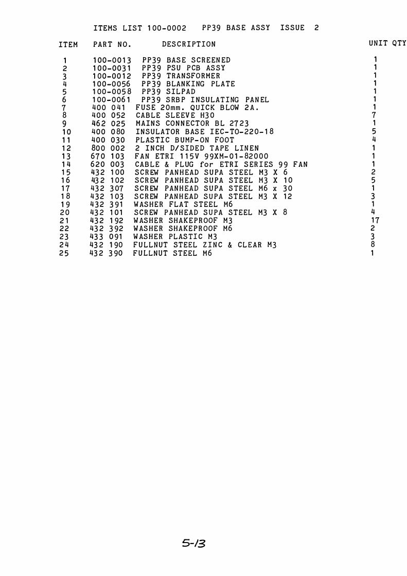
I TEMS L I S T 1 0 0 - 0 0 0 2 P P 3 9 BAS E A S S Y I S S U E 2
PA R T N O .
1 0 0 -0 0 1 3 1 0 0 - 0 0 3 1 1 0 0 - 0 0 1 2 1 0 0 -0 0 56 1 0 0 - 0 0 5 8 1 0 0 - 0 06 1 4 0 0 0 4 1 4 0 0 0 52 4 6 2 0 2 5 4 0 0 0 80 4 0 0 0 3 0 Bo o o o 2 6 7 0 1 0 3 6 2 0 0 0 3 4 3 2 1 0 0 43 2 1 0 2 4 3 2 3 07 4 3 2 1 0 3 4 3 2 3 9 1 4 3 2 1 0 1 4 3 2 1 92 4 3 2 3 9 2 4 3 3 0 9 1 43 2 1 90 43 2 3 90
D ES C R I P T I O N
P P 3 9 BAS E S C R E E N ED P P 3 9 PS U P CB AS S Y P P 3 9 T R A N SFO R M E R P P 3 9 B LA N K I NG P L A T E P P 3 9 S I L PA D P P 3 9 S RB P I N S U L AT I NG PA N EL
F U S E 2 0 mm . Q U I C K B LOW 2 A . C A B L E S L E EV E H 3 0 M A I N S CO N N E C T O R B L 27 2 3 I N S U L A T O R B AS E I E C - T0- 2 2 0 - 1 8 P L AS T I C B U M P - O N FO O T 2 I N CH D/ S I D E D T A P E L I N E N F A N E T R I 1 1 5 V 9 9X M- 0 1 - 82 0 0 0 CAB L E & P L UG f or E T R I S E R I ES 9 9 F A N S C R EW P A N H EAD S U PA S T E E L M 3 X 6 S C R EW P A N H EAD S U P A S T E E L M 3 X 1 0 S C R EW P A N H EA D S U P A S T E E L M 6 x 3 0 S C R EW P A N H EAD S U P A S T E E L M3 X 1 2 W AS H E R F L A T S T E E L M 6 S C R EW P A N H E A D S U PA S T E E L M3 X 8 W AS H E R S H A K E P R O OF M 3 W AS H E R S H A K E P R O O F M 6 W AS H E R P L AS T I C M 3 F U L L N U T S T E E L Z I N C & C L E A R M 3 F U L L N U T S T E E L M 6
5-13
U N I T Q TY
1 1 1 1 1 1 1 7 1 5 4 1 1 1 2 5 1 3 1 4 1 7 2 3 8 1

I T E M
1 2 3 4 5 6
I T EMS L IS T 1 0 0 - 0 0 1 5 P P 3 9 H/ S I N K AS S Y ( 8T R S ) I S S U E 2
P A R T N O .
1 0 0 - 0 0 6 2 1 0 0 - 0 0 6 4 2 90 2 5 1 4 3 2 1 0 3 4 3 2 1 92 4 3 2 1 90
DE S C R I P T I O N
8 T R A N S I S TO R H EATS I N K 8 T R A N S I S TO R S I L P A D P P 3 9
T R A N S I S T O R MJ E 2 5 1 S C R EW PAN H EAD S U PA S T E E L M 3 X 1 2 W AS H E R S H A K E P R O O F M 3 F U L L N U T S TE E L Z I N C & C L E A R M 3
5- 14-
U N I T Q TY
1 2 8 4 8 4

I T E M
1 2 3 4 5 6
I T E M S L I S T 1 0 0 - 0 0 1 6 P P 3 9 H/ S I N K A S S Y ( 3 T R S ) I S S U E 1
PA R T N O .
1 0 0 - 0 0 6 3 1 0 0 - 0 0 6 5 2 90 2 5 1 43 2 1 02 4 3 2 1 92 4 3 2 1 90
D E S C R I PT I O N
3 T R A N S I S TO R H E ATS I N K 3 T R A N S I S TO R S I L P A D P P 3 9
TR A N S I S TO R MJ E 2 5 1 S C R EW PAN H EAD S U PA S T E E L M3 X 1 0 W AS H E R S H AK E P R O O F M 3 F U L L N U T S T E EL Z I N C & C L E A R M3
5-15
U N I T Q TY
1 1 3 3 6 3

I T EM S L I S T 1 0 0 - 0 0 1 4 P P 3 9 C / F O R M MAI N B D/ P S U IS S U E 2
I T E M P A R T N O .
1 4 9 1 6 1 7 1 8 1 9 2 0 2 1 2 2 2 3
4 6 2 0 4 1 46 2 0 1 5 4 0 0 0 4 9 6 80 0 0 9 6 80 0 1 0 6 80 0 1 1 6 80 0 1 5 6 80 0 2 1 6 80 0 1 3 6 80 0 1 4 6 80 0 2 2
D E S C R I P T I O N
M O L EX C O N N EC T O R 1 1 W AY 1 0 - 0 1 - 1 1 1 4 MO L EX C O N TA C T 6 83 8 TL CAB L E TI E TYB 2 3 M W I R E R ED 2 4/ 0 . 2 W I R E G R EY 2 4/ 0 . 2 W I R E B LA C K 2 4/ 0 . 2 PV C EQ U I P . W I R E 2 4 / 0 . 2 m m G R E EN EQ U I P W I R E 2 4 / 0 . 2 mm B L U E W I R E B ROW N 1 6 / 0 . 2 W I R E O R A NG E 1 6 / 0 . 2 PV C EQ U I P W I R E 2 4 / 0 . 2 Y E L LOW
5-16
U N I T Q TY
1 1 0 1 1 1 1 1 1 1 1 1

I T E M
1 2 3 4 5 6 7 8 9 1 0 1 1 1 2 1 3 1 4 1 5 1 6 1 7 1 8 1 9 2 0 2 1 2 2 2 3
I T EMS L I S T 1 0 0 - 0 0 3 1 P P 3 9 PS U P CB IS S U E 3
PA R T N O .
1 3 1 1 83 1 3 1 2 2 3 1 3 1 4 7 2 1 3 1 5 6 2 1 3 4 2 4 1 1 3 4 6 82 1 1 0 0 1 9 1 1 0 0 3 9 1 1 0 0 4 0 1 1 0 0 4 2 1 2 0 1 0 2 1 2 3 1 0 0 1 2 9 47 0 3 0 6 2 1 5 3 0 6 3 1 7 3 0 6 4 0 5 1 6 6 1 0 3 46 2 0 40 1 0 0 - 0 0 3 2 26 0 0 0 4 2 6 0 0 0 5 4 0 0 0 6 0 4 3 4 0 0 4
D E S C R I PT I O N
R ES I S TO R C A R B O N F I L M 0 . 2 5W 5 % 1 8 K R ES I S TO R C A R B O N FI L M 0 . 2 5W 5 % 2 2 K R ES I S TO R C A R B O N F I L M 0 . 2 5W 5 % 4 K7 R ES I S TO R C A R B O N F I L M 0 . 2 5W 5 % 5 K 6 R ES I S TO R M E TA L F I L M 0 . 2 5W 1 % 2 4 0 R R ES I S TO R M E TA L F I L M 0 . 2 5W 1 % 6 K 8 C A P A L U M E L E C T O L YT I C 1 0 0 0 u F 2 5 V CA P A L EL E C AX I A L 47 0 0 u F 1 6 V C A P A L EL E C AX I A L 1 0 0 0 u F 6 3 V C A P A L EL E C AX I A L 2 2 0 0 u F 2 5 V CA P R E S I N DI P P E D TA N T 1 0 u F 3 5 V C A P M U LT I L AY E R C E R A M I C 0 . 1 u F 5 0 V C A P . S E R I ES Y 0 . 0 0 47 u F 2 5 0 V a c V O L TAG E R EG U LA T O R L M 3 2 0 T 1 5 V OL TAG E R EG U LATO R L M3 1 7 T V O L TAG E R EG U L ATO R L M 3 4 0 T5 P O T C E R M E T 3 / 8 i n SQ 1 0K MO L EX C O N N E C T O R 1 1 W AY 1 0 - 1 6 - 1 1 1 1 P P 3 9 PS U P CB R E CT I F I E R W 02 R E C T I F I E R KB P C 1 0 2 S OL D E R P I N D/ S P I EZ O A L A R M PKB 8 - 4 AO
5-1 7
U NI T Q TY
1 1 1 1 3 1 1 2 2 1 2 5 3 1 3 1 2 2 1 3 1 4 1

6 . 0 Component Locat ion
6 . 1 6 . 2
Ma i nboa rd PSU Boa rd
6 -/
1 00-002 1 1 00-003 1


7.0 Circuit Diagrams
7.1 7.2
PP39 Mainboard PP39 PSU Board
7-/
100-0021 100-0031


8.1 39H100 Module
8 . 1 .1 Component List 8 .1 .2 Items List 8 .1 .3 Circuit Diagram
8-/

COMPONENT LIST 105-0001 39M100 PCB ASSY ISSUE 3
CON 1 CON 2 CON 3 CON 4 LED 1 LED 2
LED 3 LED 4 re 1 re 2 IC 3 re 4 re 5 re 6 re 7 VR 1 R 1 R 2 R 3 R 4 R 5 R 6 R 7 R 8 0 1 D 2 D 3 D 4 D 5 D 6 D 7 c 1 c 2 c 8 c 9 c 10 c 11 c 12 c 13 c 1 4 M 1 M 2
401 128 401 128 462 104 462 104 309 209 309 209 309 209 309 209 401 428 323 373 323 373 313 000 3 13 122 172 221 172 221 167 1 0 4 131 472 131 224 131 221 131 221 131 271 131 271 131 271 131 271 284 148 284 1 48 284 148 2 84 1 48 2 84 1 48 2 84 1 48 284 1 48 123 100 123 012 124 103 124 103 124 1 03 124 103 12 4 103 124 103 124 103 318 7256 105-0002
8-2
TEXTOOL SOCKET 28 WAY TEXTOOL SOCKET 28 WAY CONNECTOR DIN MALE 48 WAY CONNECTOR DIN MALE 48 WAY LED TIL 209 LED TIL 209 LED TIL 209 LED TIL 209 28 WAY OIL CARRIER A28-KT-103d/HZ CMOS DIGITAL IC 74HC373 CMOS DIGITAL IC 74HC373 IC DIGITAL 7 4LS SERIES 7 4LSOO IC DIGITAL 7 4LS SERIES 74LS122 RESISTOR NETWORK 8RS 220R RESISTOR NETWORK 8RS 220R POT CITEC MPWT lOOK RESISTOR CARBON FILM 0. 25W 5$ 4K7 RESISTOR CARBON FILM 0. 25W 5$ 220K RESISTOR CARBON FILM 0. 25W 5$ 220R RESISTOR CARBON FILM 0. 25W 5$ 220R RESISTOR CARBON FILM 0. 25W 5$ 270R RESISTOR CARBON FILM 0. 25W 5$ 270R RESISTOR CARBON FILM 0. 25W 5$ 270ft RESISTOR CARBON FILM 0. 25W 5$ 270R DIODE 1 N4148 DIODE 1 N41 48 DIODE 1 N41 48 DIODE 1N 4148 DIODE 1N4148 DIODE 1 N41 48 DIODE 1 N41 48 CAP MULTILAYER CERAMIC 0. 1uF 50V CAP CERAMIC PLATE 4. 7pF 63V CAP MULTILAYER CERAMIC 10000pF 50V CAP MULTILAYER CERAMIC 10000pF 50V CAP MULTILAYER CERAMIC 10000pF 50V CAP MULTILAYER CERAMIC 10000pF 50V CAP MULTILAYER CERAMIC 10000pF 50V CAP MULTILAYER CERAMIC 10000pF 50V CAP MULTILAYER CERAMIC 10000pF 50V 256K E-PROM PP39 39M100 PCB

ITEMS LIST 105-0008 39M100 MODULE ASSY ISSUE 2
ITEM PART NO. DESCRIPTION UNIT QTY
1 105-0001 39M100 PCB ASSY 1 2 105-0009 PP39 39M100 TEXTOOL COVER SCREENED 1 3 100-0051 PP39 TEXTOOL COVER MOULDING 1 12 43 2 1 03 SCREW PANHEAD SUPA STEEL M3 X 12 5 20 432 192 WASHER SHAKEPROOF M3 5
8-3

ITEM
1 2 3 � 5 6 7 8 9 10 1 1 12 13 1 � 15 16 17 18 1 9
ITEMS LIST 105-0001 39M100 PCB ASSY ISSUE 3
PART NO.
131 221 131 22� 131 271 131 l.l7 2 2 8� 1 48 172 221 313 000 3 13 122 323 373 �01 �28 123 012 123 100 12� 1 03 167 1 0� �01 128 �62 1 0� 3 09 209 105-0002 318 7256
DESCRIPTION
RESISTOR CARBON FILM 0.25W 5% 220R RESISTOR CARBON FILM 0.25W 5% 220K RESISTOR CARBON FILM 0.25W 5% 270R RESISTOR CARBON FILM 0.25W 5% �K7 DIODE 1 N�1 �8 RESISTOR NETWORK 8RS 220R IC DIGITAL 7�LS SERIES 7�LSOO IC DIGITAL 7�LS SERIES 7�LS122 CMOS DIGITAL IC 7�HC373 28 WAY DIL CARRIER A28-KT-103d/HZ CAP CERAMIC PLATE �.7pF 63V CAP MULTILAYER CERAMIC 0.1uF 50V CAP MULTILAYER CERAMIC 10000pF 50V POT CITEC MPWT 100K TEXTOOL SOCKET 28 WAY CONNECTOR DIN MALE �8 WAY LED TIL 209 PP39 39M100 PCB 256K E-PROM
8-4-
UNIT QTY
2 1 4 1 7 2 1 1 2 1 1 1 7 1 2 2 � 1 1


8 .2 3 9H200 Hodul e
8.2 .1 8.2.2 8.2.3
Component List !tans Lists Circuit Diagran
8-6

COMPONENT LIST 105-0211 39M200 PCB ASSY ISSUE 1
CON 1 CON 2 LED 1 LED 2 LED 3 LED 4 IC 1 IC 2 IC 3 IC 4 IC 5 IC 6 IC 7 IC 8 IC 9 IC 10 IC 11 IC 12 IC 13 re 14 IC 15 T R 1 DN 1 R 1 R 2 R 3 R 4 R 5 R 6 R 7 R 8 D 1 D 2 D 3 D 4 D 5 D 6 D 7 c 1 c 2 c 3 c 4 c 5 c 6 c 7 c 8 c 9 c 10 c 11 M 1 M 2 M 12 M 15
46 2 1 04 46 2 1 04 309 209 309 209 309 209 309 209 310 136 313 109 313 373 313 373 321 040 105-0208 105-0207 401 1 40 401 140 401 140 401 128 401 024 317 116 317 116 401 02 8 290 056 10-0150 131 271 131 271 131 271 131 271 131 47 1 131 47 1 131 471 131 1 02 284 148 2 84 1 48 284 1 48 284 148 2 84 148 2 84 1 48 2 84 1 48 124 103 124 103 124 1 03 124 1 03 1 24 1 03 124 1 03 124 1 03 123 100 123 100 123 100 123 100 105-0212 340 004 318 716 318 7256
8-7
CONNECTOR DIN MALE 48 WAY CONNECTO R DIN MALE 48 WAY LED TIL 209 LED TIL 209 LED TIL 209 LED TIL 209 IC DIGITAL 74 SERIES 74136 IC DIGITAL 74LS SERIES 74LS109 IC DIGITAL 74LS SE RIES 74LS373 IC DIGITAL 74LS SERIES 74LS373 DIGITAL CMOS CD4040B FPLA 82S153 39M200 IC6 FPLA 82S153 39M200 IC7 TEXTOOL SOCKET 40 WAY TEXTOOL SOCKET 40 WAY TEXTOOL SOCKET 40 WAY TEXTOOL SOCKET 28 WAY OIL SOCKET 24 WAY RAM 6116 RAM 6116 DIL SOCKET 28 WAY TRANSISTO R MPS A56 8 PIN DIODE PACK 1N4150 RESISTO R CA RBON FILM 0.25W 5S 270R RESISTOR CARBON FILM 0.25W 5S 270R RESISTO R CARBON FILM 0. 25W 5S 270R RESISTOR CARBON FILM 0.25W 5S 270R RESISTOR CARBON FILM 0.25W 5S 470R RESISTOR CARBON FILM 0.25W 5% 470R RESISTOR CARBON FILM 0.25W 5% 470R RESISTOR CARBON FILM 0. 25W 5% 1KO DIODE 1N4148 DIODE 1N4148 DIODE 1 N4148 DIODE 1 N41 48 DIODE 1 N4148 DIODE 1N4148 DIODE 1N4148 CAP MULTILAYE R CERAMIC 10000pF 50V CAP MULTILAYE R CERAMIC 10000pF 50V CAP MULTILAYE R CERAMIC 10000pF 50V CAP MULTILAYE R CERAMIC 10000pF 50V CAP MULTILAYER CERAMIC 10000pF 50V CAP MULTILAYE R CE RAMIC 10000pF 50V CAP MULTILAYE R CE RAMIC 10000pF 50V CAP MULTILAYE R CE RAMIC 0. 1uF 50V CAP MULTILAYE R CE RAMIC 0.1uF 50V CAP MULTILAYE R CE RAMIC 0.1uF 50V CAP MULTILAYE R CE RAMIC 0.1uF 50V PP39 39M200 PCB RELAY RS 349 399 FORM C EPROM 2716 256K E-PROM

ITEMS LIST 105-0211 39M200 PCB ASSY ISSUE 1
ITEM PART NO.
1 1 3 1 1 02 2 1 3 1 271 3 1 3 1 47 1 4 284 1 48 5 1 05-0207 6 1 05-0208 7 3 1 0 1 36 8 3 1 3 1 09 9 3 1 3 373 1 0 3 1 7 1 1 6 1 1 321 040 1 2 401 024 1 3 40 1 028 1 4 40 1 1 28 1 5 40 1 1 40 1 6 1 23 1 00 1 7 124 1 03 1 8 2 90 056 1 9 462 1 04 20 309 209 2 1 1 0-0 1 50 22 1 05-02 1 2 23 3 1 8 7 1 6 24 3 1 8 7256 25 340 004
DESCRIPTION
RESISTOR CARBON FILM 0.25W 5% 1KO RESISTOR CARBON FILM 0.25W 5% 270R RESISTOR CARBON FILM 0.25W 5% 470R DIODE 1 N4148 FPLA 82S153 39M200 IC7 FPLA 82S153 39M200 IC6 IC DIGITAL 74 SERIES 74136 IC DIGITAL 74LS SERIES 74LS109 IC DIGITAL 74LS SERIES 74LS373 RAM 6 1 16 DIGITAL CMOS CD4040B OIL SOCKET 24 WAY OIL SOCKET 28 WAY TEXTOOL SOCKET 28 WAY TEXTOOL SOCKET 40 WAY CAP MULTILAYER CERAMIC 0. 1 uF 50V CAP MULTILAYER CERAMIC 1 0000pF 50V TRANSISTOR MPS A56 CONNECTOR DIN MALE 48 WAY LED TIL 209 8 PIN DIODE PACK 1N4 1 50 PP3 9 3 9M200 PCB EPROM 271 6 256K E-PROM RELAY RS 349 399 FORM C
UNIT QTY
1 4 3 7 1 1 1 1 2 2 1 1 1 1 3 4 7 1 2 4 1 1 1 1 1
