stable operation of a single phase cascaded … · the proposed paper presents the steady state...
TRANSCRIPT

International Journal of Advances in Engineering & Technology, July 2012.
©IJAET ISSN: 2231-1963
206 Vol. 4, Issue 1, pp. 206-216
STABLE OPERATION OF A SINGLE - PHASE CASCADED H-
BRIDGE MULTILEVEL CONVERTER
V. Komali1
and P. Pawan Puthra2
1Assistant Prof., Dhanekula Institute of Engg. & Tech., Vijayawada, India
2Assistant Prof., Gayatri Vidya Parishad College of Engg. & Tech., Visakhapatnam, India
ABSTRACT
The proposed paper presents the steady state power balance in the cells of a single-phase two cell cascaded H-
Bridge converter. Multilevel cascaded H-Bridge (CHB) converters fonds a good solution for high-power
applications. The power balance can be achieved by supplying the active power from the grid or to deliver
active power to the grid in each cell. This can be analyzed by maintaining the DC-link voltages and the desired
AC output voltage value. To have a stable operation it is necessary to supply the active power to 2C-CHB
between maximum and minimum limits. The circuit for 2C-CHB synchronous rectifier is designed in MATLAB
and the results are obtained successfully.
KEYWORDS: Cascaded Converters, Multilevel systems.
I. INTRODUCTION
MULTILEVEL converters have turned into a mature technology that has increased its use in the last
years. [1]-[3]. Among the multilevel converter topologies, the Cascaded H-Bridge (CHB) converters
were first presented in 1975.Since then, the research works have paid attention in this topology
because it presents several advantages compared with other multilevel converter topologies in terms
of modularity, Simplicity, and the number of levels with a minimum number of power
semiconductors [4]
The CHB has been used to develop different applications, such as synchronous rectifiers, inverters,
Statcoms, active filters, renewable energy integration systems, motor drives, etc. [5]-[10]. Moreover,
specific control strategies and modulation techniques, associated with those applications, have been
designed for this converter topology.[11]-[13]. As each DC link is independent, when the CHB
converter is used as a synchronous rectifier, it is possible to connect loads with several values to each
DC link. In addition, each DC link can be controlled to a different DC voltage level providing a high
degree of freedom. When two or more DC voltage values are needed, although it is possible to use
independent two-level converters, the CHB converter provides some extra benefits. It has a lower
input current harmonic content; thus, a lower smoothing inductor Value can be used. Therefore, the
CHB provides reduction in the overall volume, weight, and economical cost. For these reasons, the
CHB topology is very suitable when two or more DC voltage levels are needed. However, the
converter operation has to be taken into account in the design process. Due to the fact that every cell
shares the same input AC current, the loading condition of each cell affects the behavior of the overall
system.
International Journal of Advances in Engineering & Technology, July 2012.
©IJAET ISSN: 2231-1963
207 Vol. 4, Issue 1, pp. 206-216
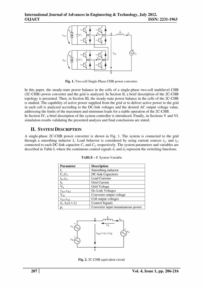
Fig. 1. Two-cell Single-Phase CHB power converter.
In this paper, the steady-state power balance in the cells of a single-phase two-cell multilevel CHB
(2C-CHB) power converter and the grid is analyzed. In Section II, a brief description of the 2C-CHB
topology is presented. Then, in Section III, the steady-state power balance in the cells of the 2C-CHB
is studied. The capability of active power supplied from the grid or to deliver active power to the grid
in each cell is analyzed according to the DC-link voltages and the desired AC output voltage value,
addressing the limits of the maximum and minimum loads for a stable operation of the 2C-CHB.
In Section IV, a brief description of the system controller is introduced. Finally, in Sections V and VI,
simulation results validating the presented analysis and final conclusions are stated.
II. SYSTEM DESCRIPTION
A single-phase 2C-CHB power converter is shown in Fig. 1. The system is connected to the grid
through a smoothing inductor L. Load behavior is considered by using current sources iL1 and iL2
connected to each DC-link capacitor C1 and C2, respectively. The system parameters and variables are
described in Table I, where the continuous control signals δ1 and δ2 represent the switching functions.
TABLE – I System Variable
Parameter Description
L Smoothing inductor
C1,C2 DC-link Capacitors
iL1,iL2 Load Currents
IS Grid Current
VS Grid Voltage
vdc1,vdc2 Dc-Link Voltages
Vab Converter output voltage
vm1,vm2 Cell output voltages
δ1, δ2є[-1,1] Control Signals
pt Converter input instantaneous power
Fig. 2. 2C-CHB equivalent circuit
International Journal of Advances in Engineering & Technology, July 2012.
©IJAET
208
The equations that describe the 2C
previously.
The behavior of 2C-CHB is characterized by the inductor current dynamic (4) and DC
voltage dynamic in each cell (5) and (6). In these equations, signals
voltages of each cell. These voltages depend on the DC
each cell. Moreover, signals p1
current sources connected to each cell, respectively.
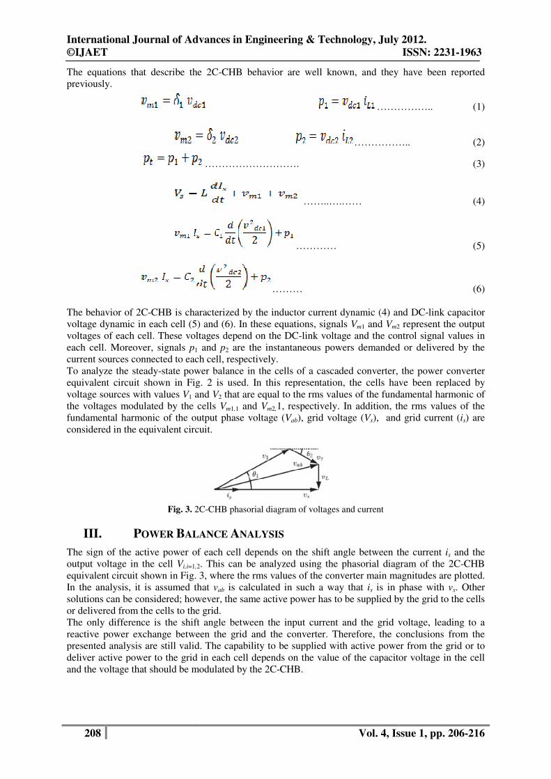
To analyze the steady-state power balance in the cells of
equivalent circuit shown in Fig. 2 is used. In this representation, the cells have been replaced by
voltage sources with values V1 and
the voltages modulated by the cells
fundamental harmonic of the output phase voltage (
considered in the equivalent circuit.
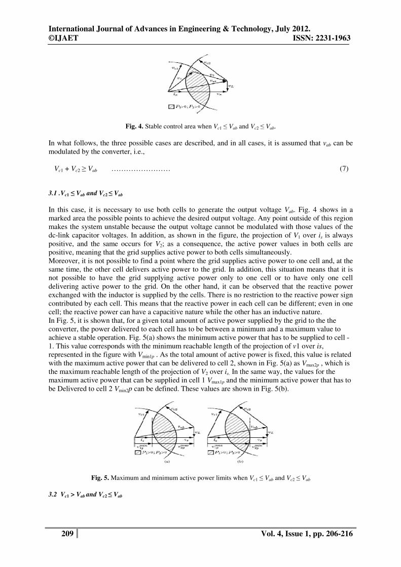
Fig. 3. 2C
III. POWER BALANCE
The sign of the active power of each cell depends on the shift angle between the current
output voltage in the cell Vi,i=1,2
equivalent circuit shown in Fig. 3, where the rms values of the converter main magnitudes are plotted.
In the analysis, it is assumed that
solutions can be considered; however, the same active power has to be supplied by the grid to the cells
or delivered from the cells to the grid.
The only difference is the shift angle between the input current and the grid voltage, leading to a
reactive power exchange between the g
presented analysis are still valid. The capability to be supplied with active power from the grid or to
deliver active power to the grid in each cell depends on the value of the capacitor voltage i
and the voltage that should be modulated by the 2C
International Journal of Advances in Engineering & Technology, July 2012.
Vol. 4, Issue 1, pp.
The equations that describe the 2C-CHB behavior are well known, and they have been reported
……………..
……………..
……………………….
……..….……
…………
………
CHB is characterized by the inductor current dynamic (4) and DC
voltage dynamic in each cell (5) and (6). In these equations, signals Vm1 and Vm2
voltages of each cell. These voltages depend on the DC-link voltage and the control signal values in
and p2 are the instantaneous powers demanded or delivered by the
current sources connected to each cell, respectively.
state power balance in the cells of a cascaded converter, the power converter
equivalent circuit shown in Fig. 2 is used. In this representation, the cells have been replaced by
and V2 that are equal to the rms values of the fundamental harmonic of
modulated by the cells Vm1,1 and Vm2,1, respectively. In addition, the rms values of the
fundamental harmonic of the output phase voltage (Vab), grid voltage (Vs), and grid current (
considered in the equivalent circuit.
2C-CHB phasorial diagram of voltages and current
ALANCE ANALYSIS
The sign of the active power of each cell depends on the shift angle between the current
2. This can be analyzed using the phasorial diagram of the 2C
equivalent circuit shown in Fig. 3, where the rms values of the converter main magnitudes are plotted.
In the analysis, it is assumed that vab is calculated in such a way that is is in phase with
; however, the same active power has to be supplied by the grid to the cells
or delivered from the cells to the grid.
The only difference is the shift angle between the input current and the grid voltage, leading to a
reactive power exchange between the grid and the converter. Therefore, the conclusions from the
presented analysis are still valid. The capability to be supplied with active power from the grid or to
deliver active power to the grid in each cell depends on the value of the capacitor voltage i
and the voltage that should be modulated by the 2C-CHB.
International Journal of Advances in Engineering & Technology, July 2012.
ISSN: 2231-1963
Vol. 4, Issue 1, pp. 206-216
CHB behavior are well known, and they have been reported
…………….. (1)
…………….. (2)
(3)
(4)
(5)
(6)
CHB is characterized by the inductor current dynamic (4) and DC-link capacitor
2 represent the output
link voltage and the control signal values in
are the instantaneous powers demanded or delivered by the
a cascaded converter, the power converter
equivalent circuit shown in Fig. 2 is used. In this representation, the cells have been replaced by
that are equal to the rms values of the fundamental harmonic of
1, respectively. In addition, the rms values of the
), and grid current (is) are
The sign of the active power of each cell depends on the shift angle between the current is and the
diagram of the 2C-CHB
equivalent circuit shown in Fig. 3, where the rms values of the converter main magnitudes are plotted.
is in phase with vs. Other
; however, the same active power has to be supplied by the grid to the cells
The only difference is the shift angle between the input current and the grid voltage, leading to a
rid and the converter. Therefore, the conclusions from the
presented analysis are still valid. The capability to be supplied with active power from the grid or to
deliver active power to the grid in each cell depends on the value of the capacitor voltage in the cell
International Journal of Advances in Engineering & Technology, July 2012.
©IJAET ISSN: 2231-1963
209 Vol. 4, Issue 1, pp. 206-216
Fig. 4. Stable control area when Vc1 ≤ Vab and Vc2 ≤ Vab.
In what follows, the three possible cases are described, and in all cases, it is assumed that vab can be
modulated by the converter, i.e.,
Vc1 + Vc2 ≥ Vab …………………… (7)
3.1 .Vc1 ≤ Vab and Vc2 ≤ Vab
In this case, it is necessary to use both cells to generate the output voltage Vab. Fig. 4 shows in a
marked area the possible points to achieve the desired output voltage. Any point outside of this region
makes the system unstable because the output voltage cannot be modulated with those values of the
dc-link capacitor voltages. In addition, as shown in the figure, the projection of V1 over is is always
positive, and the same occurs for V2; as a consequence, the active power values in both cells are
positive, meaning that the grid supplies active power to both cells simultaneously.
Moreover, it is not possible to find a point where the grid supplies active power to one cell and, at the
same time, the other cell delivers active power to the grid. In addition, this situation means that it is
not possible to have the grid supplying active power only to one cell or to have only one cell
delivering active power to the grid. On the other hand, it can be observed that the reactive power
exchanged with the inductor is supplied by the cells. There is no restriction to the reactive power sign
contributed by each cell. This means that the reactive power in each cell can be different; even in one
cell; the reactive power can have a capacitive nature while the other has an inductive nature.
In Fig. 5, it is shown that, for a given total amount of active power supplied by the grid to the the
converter, the power delivered to each cell has to be between a minimum and a maximum value to
achieve a stable operation. Fig. 5(a) shows the minimum active power that has to be supplied to cell -
1. This value corresponds with the minimum reachable length of the projection of v1 over is,
represented in the figure with Vmin1p . As the total amount of active power is fixed, this value is related
with the maximum active power that can be delivered to cell 2, shown in Fig. 5(a) as Vmax2p , which is
the maximum reachable length of the projection of V2 over is. In the same way, the values for the
maximum active power that can be supplied in cell 1 Vmax1p and the minimum active power that has to
be Delivered to cell 2 Vmin2p can be defined. These values are shown in Fig. 5(b).
Fig. 5. Maximum and minimum active power limits when Vc1 ≤ Vab and Vc2 ≤ Vab
3.2 Vc1 > Vab and Vc2 ≤ Vab

International Journal of Advances in Engineering & Technology, July 2012.
©IJAET ISSN: 2231-1963
210 Vol. 4, Issue 1, pp. 206-216
In this case, the desired output voltage can be achieved using both cells or just using the cell with the
higher dc voltage. This allows two possible power balance situations in the cells. In Fig. 6, the marked
area represents the points where both cells are supplied with active power from the grid, while the
marked area shows the points where the first cell is supplied with active power from the grid while the
second cell delivers active power to the grid. As in Section III-A, the reactive power is exchanged
between the inductor and the cells without restrictions in the reactive power sign contributed by each
one.
Fig. 6(a) shows a possible solution with both cells supplied with active power from the grid, and Fig.
6(b) shows a possible solution when the first cell is supplied from the grid while the second cell
delivers active power to the grid. It is worth noting that, when Vc1 > Vab and Vc2 ≤ Vab, if the total
active power supplied to the converter from the grid is positive, then only the second cell active power
can be negative, while the first cell active power is positive; it is not possible to have a negative active
power in the first cell while the second cell has a positive active power value.
Fig. 6. Stable control area when Vc1 > Vab and Vc2 ≤ Vab. (From top to bottom) Possible solution with (a) P1 > 0
and P2 > 0, and (b) P1 > 0 and P2 < 0.
Fig. 7 shows the limits for the maximum and minimum active power values allowed in the cells to
achieve a stable operation, when the total amount of active power supplied from the grid to the
converter is fixed. Two different power balance situations can be clearly identified.
The first one can be considered as the conventional operation of the converter, and it is shown in Fig.
7(a). In this case, both cells are supplied from the grid, and as a consequence, a minimum active
power has to be supplied to cell 1 from the grid; this value corresponds with the minimum reachable
length of the projection of v1 over is, represented in the figure with Vmin1p . Associated with this value
is Vmax2p, which is the maximum reachable length of the projection of V2 over is and represents the
maximum active power that can be supplied to cell 2.
The second power balance situation, shown in Fig. 7(b), implies that the active powers in each cell
have different signs. Thus, the cell with the higher dc voltage is supplied from the grid, while the
other cell is delivering active power to the grid.
Under this situation, the values for the maximum active power that can be delivered to cell 1 vmax1p
and the minimum active power that has to be supplied to cell 2 Vmin2p can be defined. In Fig. 7(b), it
can be noticed that Vmin2p has opposite direction than is; thus, the second cell is delivering active
power.
Moreover, the maximum active power supplied to cell 1 is higher than the total amount of active
powers delivered from the grid. This means that the active power delivered from the second cell is
going into the first cell.
International Journal of Advances in Engineering & Technology, July 2012.
©IJAET ISSN: 2231-1963
211 Vol. 4, Issue 1, pp. 206-216
Fig. 7. Maximum and Minimum active power limits when Vc1 > Vab and Vc2 ≤ Vab.
3.3 Vc1 > Vab and Vc2 > Vab
In this case, the output voltage can be modulated using both cells or just using one of them. As a
consequence, three possible power balance situations in the cells are under concern. In the marked
area of Fig. 8, both cells are supplied simultaneously with active power from the grid, whereas the
marked area shows the set of points where the first cell is supplied with active power from the grid
while the second cell delivers active power to the grid. On the other hand, the marked area represents
the set of points where the first cell delivers active power to the grid while the second cell is supplied
with active power from the grid. Again, the reactive power is exchanged between the smoothing
inductor and the cells without restrictions in the sign of the reactive power of each cell.
Fig. 8 shows the three possible solutions, one for each power balance situation under concern. Fig.
8(a) shows the conventional operation, where both cells are supplied with active power from the grid.
Fig. 8(b) shows the converter operation when the first cell is supplied from the grid while the second
cell delivers active power to the grid. Finally, Fig. 8(c) shows a solution with the first cell delivering
active power to the grid while the second cell is supplied with active power from the grid. It can be
noticed that, when Vc1 > Vab and Vc2 > Vab, although the total active power supplied to the converter
from the grid is positive, it is possible that any one cell delivers active power to the grid while the
other one is supplied with active power from the grid. When the maximum and minimum limits of the
active power consumed or injected by the loads connected to the cells are analyzed, similar
conclusions to those presented in Section III-B, when the power balance through each cell has
different signs, are found.
Fig. 8. Stable control area when Vc1 > Vab and Vc2 > Vab. (From left to right) Possible solution with (a) P1 > 0
and P2 > 0, (b) P1 > 0 and P2 < 0, and (c) P1 < 0 and P2 > 0.
In Fig. 9, the maximum active power that can be supplied and the minimum active power values that
have to be delivered to each cell to achieve a stable operation, for a given total amount of active
powers consumed by the loads connected to the converter, are shown. Under this situation, the
minimum active power that has to be supplied in each cell is negative; thus, the cell is delivering
active power. Meanwhile, the maximum active power that can be consumed by the loads connected to
the cell is higher than the total active power supplied to the converter; thus, part of the energy
consumed in this cell comes from the other cell and not from the grid.

International Journal of Advances in Engineering & Technology, July 2012.
©IJAET ISSN: 2231-1963
212 Vol. 4, Issue 1, pp. 206-216
Fig. 9. Maximum and minimum active power limits when Vc1 > Vab and Vc2 > Vab
IV. SIMULATION RESULTS
In this section, simulation results are shown to validate the analysis presented in Section III. For this purpose, a
single phase 2C-CHB converter prototype has been used. The electric parameters of the prototype are
summarized in Table II. To assess the presented analysis, three different experiments are described. The first
one shows the converter operation in the stable region, as described in Section III-A, while the second
experiment shows the prototype behavior when the loading condition leads outside this stable operation region.
TABLE II Electric Parameters
Finally, an experiment showing the stable converter operation with both cells having opposite power balance
signs, as presented in Section III-B, is analyzed.
4.1 Stable Operation With Vc1 ≤ Vab and Vc2 ≤ Vab
In this case, both cells have to be supplied or to deliver active power from the grid simultaneously. To
illustrate this operation, a resistor of 60 Ω is connected to each dc link as a load. Several dc voltage
step references are applied to show the behavior of the 2C-CHB. Initially, the dc voltage commands
are set to 200 V. When the actual dc voltages achieve their references, the loads are connected.
Approximately 2s later, the voltage command for the first cell is changed to 300 V, and then, after 1 s,
a new reference for the second cell of 100 V is established. Fig.10. shows the real and reactive powers
of stable operation.
Fig.10. Real and reactive power
Parameter Description
RMS Grid Voltage(vs) 230 V
Grid Frequency(f) 50 HZ
Smoothing Inductance(L) 3 mH
DC -Link Capacitors(C1,C2) 2200 µF
Switching Frequency(fsw) 10 KHZ
Sampling Frequency(fs) 10 KHZ
International Journal of Advances in Engineering & Technology, July 2012.
©IJAET ISSN: 2231-1963
213 Vol. 4, Issue 1, pp. 206-216
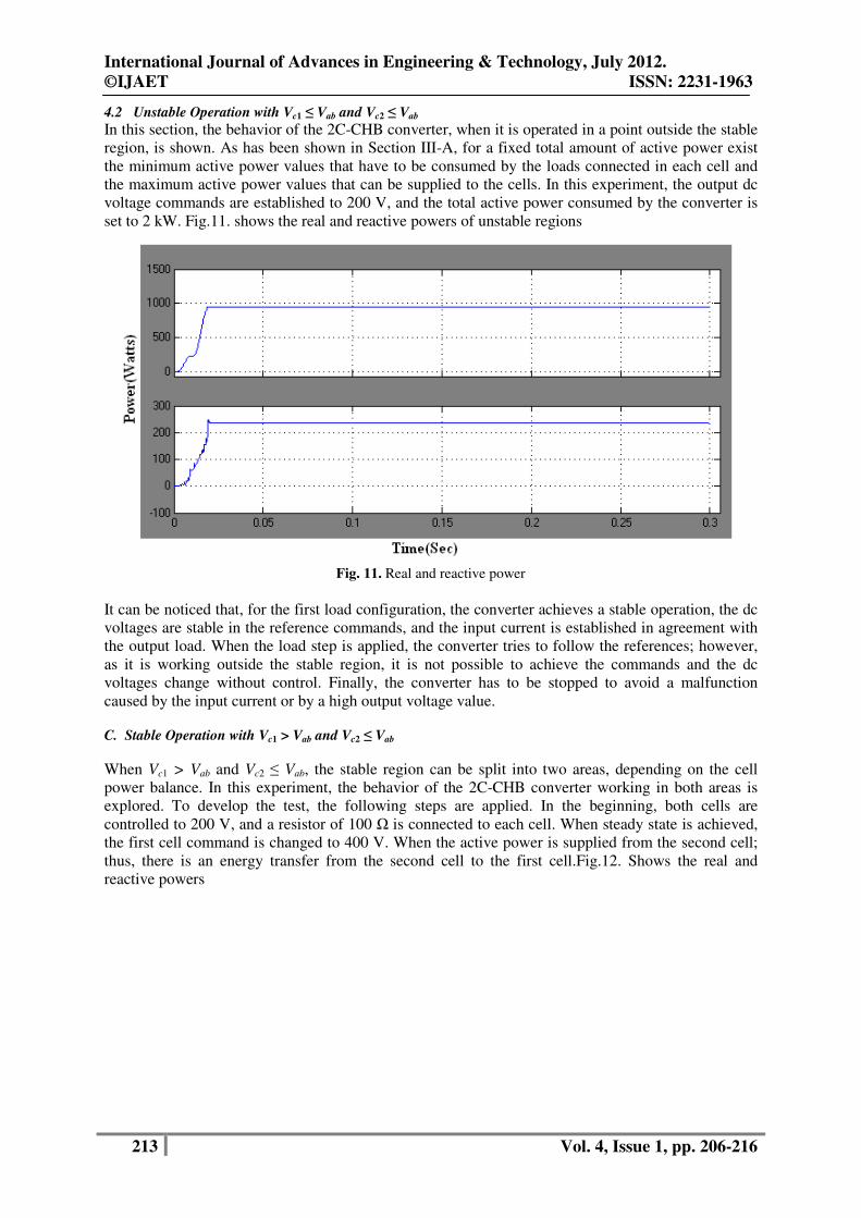
4.2 Unstable Operation with Vc1 ≤ Vab and Vc2 ≤ Vab
In this section, the behavior of the 2C-CHB converter, when it is operated in a point outside the stable
region, is shown. As has been shown in Section III-A, for a fixed total amount of active power exist
the minimum active power values that have to be consumed by the loads connected in each cell and
the maximum active power values that can be supplied to the cells. In this experiment, the output dc
voltage commands are established to 200 V, and the total active power consumed by the converter is
set to 2 kW. Fig.11. shows the real and reactive powers of unstable regions
Fig. 11. Real and reactive power
It can be noticed that, for the first load configuration, the converter achieves a stable operation, the dc
voltages are stable in the reference commands, and the input current is established in agreement with
the output load. When the load step is applied, the converter tries to follow the references; however,
as it is working outside the stable region, it is not possible to achieve the commands and the dc
voltages change without control. Finally, the converter has to be stopped to avoid a malfunction
caused by the input current or by a high output voltage value.
C. Stable Operation with Vc1 > Vab and Vc2 ≤ Vab
When Vc1 > Vab and Vc2 ≤ Vab, the stable region can be split into two areas, depending on the cell
power balance. In this experiment, the behavior of the 2C-CHB converter working in both areas is
explored. To develop the test, the following steps are applied. In the beginning, both cells are
controlled to 200 V, and a resistor of 100 Ω is connected to each cell. When steady state is achieved,
the first cell command is changed to 400 V. When the active power is supplied from the second cell;
thus, there is an energy transfer from the second cell to the first cell.Fig.12. Shows the real and
reactive powers

International Journal of Advances in Engineering & Technology, July 2012.
©IJAET ISSN: 2231-1963
214 Vol. 4, Issue 1, pp. 206-216
Fig. 12. Real and reactive power
Fig.13. Current through the grid
Fig.14. Multi level Inverter output voltage.

International Journal of Advances in Engineering & Technology, July 2012.
©IJAET ISSN: 2231-1963
215 Vol. 4, Issue 1, pp. 206-216
V. CONCLUSION
A CHB power converter is a suitable topology to be used when two or more independent dc voltage
values are needed in a synchronous rectifier or back-to-back application. However, some criteria have
to be taken into account to achieve a stable converter operation. In this paper, the power balance limits
in the cells of a single-phase 2C-CHB power converter have been addressed.
These limits depend on the dc-link voltage values It is shown that, under certain conditions, it is
possible to have opposite sign active power values simultaneously in both cells. Moreover, to have a
stable operation, it is necessary to ensure that, for a total amount of active power supplied to the 2C-
CHB, both cell loads are between the maximum and minimum allowed. Finally, simulation results are
introduced, validating that the presented analysis is an appropriate tool to establish the design criteria
for the 2C-CHB synchronous rectifier or back-to-back application.
REFERENCES [1] J. Rodriguez, S. Bernet, B. Wu, J. O. Pontt, and S. Kouro, “Multilevel voltage-source-converter
topologies for industrial medium-voltage drives,” IEEE Trans. Ind. Electron., vol. 54, no. 6, pp. 2930–
2945, Dec. 2007.
[2] L. G. Franquelo, J. Rodriguez, J. I. Leon, S. Kouro, R. Portillo, and M. M. Prats, “The age of multilevel
converters arrives,” IEEE Ind. Electron. Mag., vol. 2, no. 2, pp. 28–39, Jun. 2008.
[3] D. Krug, S. Bernet, S. S. Fazel, K. Jalili, and M. Malinowski, “Comparison of 2.3-kV medium-voltage
multilevel converters for industrial medium-voltage drives,” IEEE Trans. Ind. Electron., vol. 54, no. 6,
pp. 2979–2992, Dec. 2007.
[4] M. E. Ortuzar, R. E. Carmi, J. W. Dixon, and L. Moran, “Voltage-source active power filter based on
multilevel converter and ultracapacitor dc link,” IEEE Trans. Ind. Electron., vol. 53, no. 2, pp. 477–485,
Apr. 2006.
[5] H. Iman-Eini, J. L. Schanen, S. Farhangi, and J. Roudet, “A modular strategy for control and voltage
balancing of cascaded H-bridge rectifiers,” IEEE Trans. Power Electron., vol. 23, no. 5, pp. 2428–2442,
Sep. 2008.
[6] A. J. Watson, P. W. Wheeler, and J. C. Clare, “A complete harmonic elimination approach to dc link
voltage balancing for a cascaded multilevel rectifier,” IEEE Trans. Ind. Electron., vol. 54, no. 6, pp.
2946–2953, Dec. 2007.
[7] P. Lezana, J. Rodriguez, and D. A. Oyarzun, “Cascaded multilevel inverter with regeneration capability
and reduced number of switches,” IEEE Trans. Ind. Electron., vol. 55, no. 3, pp. 1059–1066, Mar. 2008.
[8] P. Lezana, C. A. Silva, J. Rodriguez, and M. A. Perez, “Zero-steady-stateerror input-current controller for
regenerative multilevel converters based on single-phase cells,” IEEE Trans. Ind. Electron., vol. 54, no.
2, pp. 733– 740, Apr. 2007.
[9] J. A. Barrena, L. Marroyo, M. A. R. Vidal, and J. R. T. Apraiz, “Individual voltage balancing strategy for
PWM cascaded H-bridge converterbased STATCOM,” IEEE Trans. Ind. Electron., vol. 55, no. 1, pp.
21–29, Jan. 2008.
[10] A. M. Massoud, S. J. Finney, A. J. Cruden, and B. W. William, “Threephase, three-wire, five-level
cascaded shunt active filter for power conditioning, using two different space vector modulation
techniques,” IEEE Trans. Power Del., vol. 22, no. 4, pp. 2349–2361, Oct. 2007.
[11] A. Dell’Aquila, M. Liserre, V. G. Monopoli, and P. Rotondo, “Overview of PI-based solutions for the
control of dc buses of a single-phase H-bridge multilevel active rectifier,” IEEE Trans. Ind. Appl., vol.
44, no. 3, pp. 857–866, May/Jun. 2008.
[12] M. A. Perez, P. Cortes, and J. Rodriguez, “Predictive control algorithm technique for multilevel
asymmetric cascaded H-bridge inverters,” IEEE Trans. Ind. Electron., vol. 55, no. 12, pp. 4354–4361,
Dec. 2008.
[13] J. I. Leon, S. Vazquez, A. J. Watson, P. W. Wheeler, L. G. Franquelo, and J. M. Carrasco, “Feed-forward
space vector modulation for single-phase multilevel cascaded converters with any dc voltage ratio,” IEEE
Trans. Ind. Electron., vol. 56, no. 2, pp. 315–325, Feb. 2009.
AUTHORS BIBLIOGRAPHY
V.KOMALI was born in Vijayawada in the year of 1987. She received Bachelor of
Technology from K.L.C.E in 2008. Her Master of technology in Power system control and
automation from Gayatri Vidhya Parishad College of Engineering, Visakhapatnam, A.P. in
2011. Her main research area interest in FACTS, Non-Conventional energy sources such as

International Journal of Advances in Engineering & Technology, July 2012.
©IJAET ISSN: 2231-1963
216 Vol. 4, Issue 1, pp. 206-216
photo voltaic, wind and hybrid.
P. PAWAN PUTHRA was born in Visakhapatnam in the year of 15 Nov 1983. He received
Bachelor of Technology from St. Theresa institute of technology in 2006. His Master of
Technology in specialization of Power Electronics & Drives from Vellore institute of
Technology in the year of 2008. His main research area interest in FACTS, Power Electronics,
and Non-Conventional energy sources such as photo voltaic, wind and hybrid. He is presently
working as an Assistant Professor in Gayatri Vidya parishad college of engineering in
Visakhapatnam.