stability of the master oscillator for flash at desy
TRANSCRIPT
Stability of the Master Oscillator forFLASH at DESY
Project thesis
Institut fur Hochfrequenztechnik TUHH
TESLA-FEL Report 2006-12
B.Lorbeer
October 2006
Supervisors: Prof.Dr.-Ing. Klaus SchunemannTechnische Universitat Hamburg Harburg
Dr.Stefan SimrockDeutsches Elektronen Synchrotron1(DESY)
1We acknowledge the support of the European Community-Research Infrastructure Activity under the FP6”Structuring the European Research Area” program (CARE, contract number RII3-CT-2003-506395).
Abstract
In this document a microwave master oscillator (M.O.) and a reference frequency distributionsystem for the Free Electron Laser (FEL) DESY FLASH is presented. The M.O. generatesfixed frequencies ranging from 50 Hz up to 2.856 GHz that must have a defined phase rela-tion. The long term stability (hours) is in the range of a few ps. On short time scales ( < 1sec) the measured timing jitter for generated frequencies higher than 9 MHz is smaller than100 fs. The focus is on the design of single modules of the M.O.. The established precisionmeasurements techniques used to verify the performance are presented. The measurementresults are discussed in the end.
In diesem Dokument wird ein Mikrowellen Master Oszillator (M.O.) fur den Freie Elektro-nen Laser (FEL) DESY FLASH vorgestellt. Im M.O. werden feste Frequenzen zwischen 50Hz und 2.856 GHz generiert, die eine feste Phasenbeziehung zueinander haben mussen. DieLangzeitstabilitat (Stunden) betragt mehrere ps. Die Kurzzeitstabilitat (< 1s) fur Frequen-zen grosser als 9 MHz ist kleiner als 100 fs. Das Hauptaugenmerk liegt in der Entwicklung derEinzelmodule des M.O. Die Prazisionsmesstechniken um dieses System zu bewerten werdenerlautert und die Messergebnisse werden diskutiert.

CONTENTS 3
Contents
1 Motivation 4
1.1 FLASH and XFEL [1] . . . . . . . . . . . . . . . . . . . . . . . . . . . . . . . . . 41.2 Assignment . . . . . . . . . . . . . . . . . . . . . . . . . . . . . . . . . . . . . . . 5
2 Definition of stability terms 6
2.1 Phase noise description in time and frequency domain . . . . . . . . . . . . . . . 62.2 Transmission of amplitude - and phase noise in linear networks . . . . . . . . . . 72.3 Phase noise in a mutiplier chain . . . . . . . . . . . . . . . . . . . . . . . . . . . . 72.4 Phase noise model of a phase locked loop . . . . . . . . . . . . . . . . . . . . . . 72.5 Integrated phase noise and timing jitter . . . . . . . . . . . . . . . . . . . . . . . 92.6 Drifts . . . . . . . . . . . . . . . . . . . . . . . . . . . . . . . . . . . . . . . . . . 9
3 Measurement principles 10
3.1 Phase Noise measurement using cross correlation . . . . . . . . . . . . . . . . . . 103.2 Drift measurement methods . . . . . . . . . . . . . . . . . . . . . . . . . . . . . . 11
3.2.1 Principle operation of a phasedetector . . . . . . . . . . . . . . . . . . . . 113.2.2 Drifts of a phase detector . . . . . . . . . . . . . . . . . . . . . . . . . . . 123.2.3 Drifts of an amplifier . . . . . . . . . . . . . . . . . . . . . . . . . . . . . . 143.2.4 Drifts of several RF sources . . . . . . . . . . . . . . . . . . . . . . . . . . 14
4 Master Oscillator 16
4.1 Overview . . . . . . . . . . . . . . . . . . . . . . . . . . . . . . . . . . . . . . . . 164.2 Low Power Part . . . . . . . . . . . . . . . . . . . . . . . . . . . . . . . . . . . . . 18
4.2.1 OCXO reference module . . . . . . . . . . . . . . . . . . . . . . . . . . . . 204.2.2 The 81 MHz and 108 MHz phase locked loops . . . . . . . . . . . . . . . . 224.2.3 Divider modules for 27 MHz, 13.5 MHz, 9 MHz, 1 MHz . . . . . . . . . . 354.2.4 9 MHz Power amplifier . . . . . . . . . . . . . . . . . . . . . . . . . . . . . 374.2.5 TTL drivers for 9 MHz and 1 MHz TTL signal . . . . . . . . . . . . . . . 374.2.6 Direct digital synthesis of 50 Hz . . . . . . . . . . . . . . . . . . . . . . . 38
4.3 1.3 GHz and 2.856 GHz phase locked loops . . . . . . . . . . . . . . . . . . . . . 394.3.1 1.3 GHz PLL . . . . . . . . . . . . . . . . . . . . . . . . . . . . . . . . . . 394.3.2 2.856 GHz Fractional N PLL . . . . . . . . . . . . . . . . . . . . . . . . . 45
4.4 High Power Part for amplification of 81 MHz and 1.3 GHz signals . . . . . . . . 49
5 Summary and Conclusion 50
A Blockdiagrams 53
B Programming the ADF4153 56
4 1 MOTIVATION
1 Motivation
1.1 FLASH and XFEL [1]
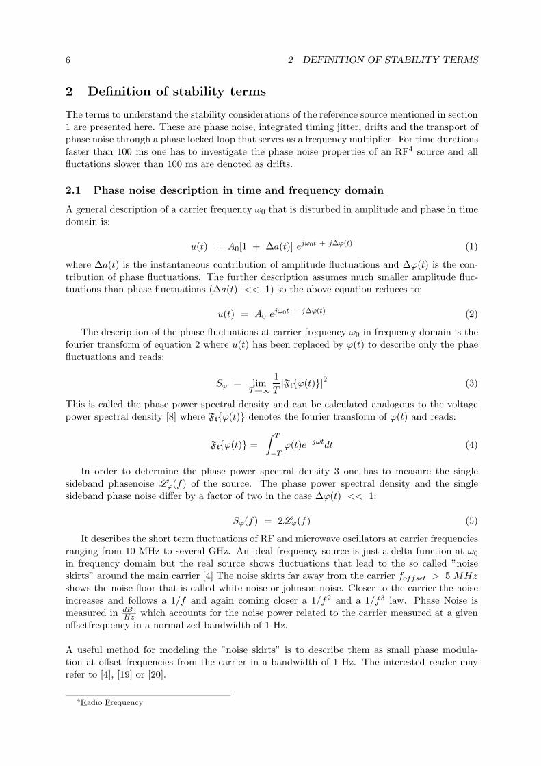
In 1993 DESY started developing the next generation linear accelerator using superconductingcavities at an accelerating frequency of 1.3 GHz called Tera Electron-Volts SuperconductingLinear Accelerator (TESLA). The accelerated electrons are used for a free electron laser (FEL)to produce coherent X-Ray light of high intensity that has many applications in research formaterial science, chemistry, biology and other sciences. The XFEL X-ray laser is being plannedas a project with European participation. For the project, an all-new research center will bebuilt on the outskirts of the town of Schenefeld (Pinneberg district) in Schleswig-Holstein. Here,the X-ray laser flashes generated in a 3.4-km-long facility will be used for research purposes. Thedimensions of the XFEL make it the world’s longest artificial light source. A test facility calledFLASH is in operation at DESY and gives the opportunity to evaluate technologies for XFEL.With the generation of coherent pulsed X-Ray radiation with wavelengths of a few nanometerand pulswidths smaller than 100 fs it is possible to explore chemical reactions dynamically andthe structure of matter at scales of a few nanometers.Figure 1 sketches the layout of FLASH at DESY.
Figure 1:
The generation of coherent X-RAY radiation is based on the SASE - effect (Self AmplifiedSpontaneous Emission). After an accleration of electron bunches up to several hundreds of MeVthe electronbunches enter an undulator where they are forced on a slalom course 2in which theygenerate the coherent radiation. The interaction of the induced radiation leads to microbunchinginside the electron bunches that are seperated by the wavelength of the radiation. At FLASH awavelength of 13 nm has been achieved.The generation of highly coherent radiation is highly sensitive to field and energy fluctuationsin the accelerator. Therefore the RF 3 fields in the accelerating structures and the varioussubsytems have to be synchronized with each other. A Master Oscillator and the distributionsystem is the source to generate all frequencies synchronous to one reference source in order toobtain the synchronization stability required.
2due to the periodicity of north - and south poles of magnets and the resulting Lorenzforce on the electronbunches
3Radio Frequency

1.2 Assignment 5
1.2 Assignment
The various distributed subsystems in the accelerator require a number of different frequenciesgenerated by one source to assure the functionality of the SASE process. The short and longterm stability of and between the various widely distributed outputs of the reference systemmust be in the order of 100 fs and 1 ps respectively [21]. The frequencies are all generatedin a reference source that is called the Master Oscillator. The theoretical treatment to judgethe stability of this Master Oscillator is studied and has been realized as a prototype for beingcommisioned at FLASH in late 2006. The single modules are presented here and have beenstudied in detail.
6 2 DEFINITION OF STABILITY TERMS
2 Definition of stability terms
The terms to understand the stability considerations of the reference source mentioned in section1 are presented here. These are phase noise, integrated timing jitter, drifts and the transport ofphase noise through a phase locked loop that serves as a frequency multiplier. For time durationsfaster than 100 ms one has to investigate the phase noise properties of an RF4 source and allfluctations slower than 100 ms are denoted as drifts.
2.1 Phase noise description in time and frequency domain
A general description of a carrier frequency ω0 that is disturbed in amplitude and phase in timedomain is:
u(t) = A0[1 + ∆a(t)] ejω0t + j∆ϕ(t) (1)
where ∆a(t) is the instantaneous contribution of amplitude fluctuations and ∆ϕ(t) is the con-tribution of phase fluctuations. The further description assumes much smaller amplitude fluc-tuations than phase fluctuations (∆a(t) << 1) so the above equation reduces to:
u(t) = A0 ejω0t + j∆ϕ(t) (2)
The description of the phase fluctuations at carrier frequency ω0 in frequency domain is thefourier transform of equation 2 where u(t) has been replaced by ϕ(t) to describe only the phaefluctuations and reads:
Sϕ = limT→∞
1
T|Ftϕ(t)|2 (3)
This is called the phase power spectral density and can be calculated analogous to the voltagepower spectral density [8] where Ftϕ(t) denotes the fourier transform of ϕ(t) and reads:
Ftϕ(t) =
∫ T
−Tϕ(t)e−jωtdt (4)
In order to determine the phase power spectral density 3 one has to measure the singlesideband phasenoise Lϕ(f) of the source. The phase power spectral density and the singlesideband phase noise differ by a factor of two in the case ∆ϕ(t) << 1:
Sϕ(f) = 2Lϕ(f) (5)
It describes the short term fluctuations of RF and microwave oscillators at carrier frequenciesranging from 10 MHz to several GHz. An ideal frequency source is just a delta function at ω0
in frequency domain but the real source shows fluctuations that lead to the so called ”noiseskirts” around the main carrier [4] The noise skirts far away from the carrier foffset > 5 MHzshows the noise floor that is called white noise or johnson noise. Closer to the carrier the noiseincreases and follows a 1/f and again coming closer a 1/f2 and a 1/f3 law. Phase Noise ismeasured in dBc
Hzwhich accounts for the noise power related to the carrier measured at a given
offsetfrequency in a normalized bandwidth of 1 Hz.
A useful method for modeling the ”noise skirts” is to describe them as small phase modula-tion at offset frequencies from the carrier in a bandwidth of 1 Hz. The interested reader mayrefer to [4], [19] or [20].
4Radio Frequency

2.2 Transmission of amplitude - and phase noise in linear networks 7
2.2 Transmission of amplitude - and phase noise in linear networks
To describe the transmission of amplitude - and phase noise from the input to the output in alinear network one makes use of a conversion matrix equation 6 that relates the amplitude - andphase fluctuations at the input of the network to the output of the network.
[∆aout
A0
∆ϕout
]
︸ ︷︷ ︸
noisy output
=
[
Kaa Kaϕ
Kϕa Kϕϕ
]
︸ ︷︷ ︸
conversion matrix
[∆ain
A0
∆ϕin
]
︸ ︷︷ ︸
noisy input
+
[∆anetwork
A0
∆ϕnetwork
]
︸ ︷︷ ︸
noisy network
(6)
Amplitude - and phase fluctuations are phasors describing the noise as an AM5 ∆a and PM6
∆ϕ at an offsetfrequency ∆ω from the carrier ω0 [5]. The amplitude of the AM contribution isnormalized to the carrier voltage A0.
The input amplitude - and phase noise is directly converted by the factors Kaa and Kϕϕ.The factors Kaϕ and Kϕa describe how an AM converts to a PM and how a PM converts to anAM. The additional vector accounts for the AM and PM noise contribution of the network.
2.3 Phase noise in a mutiplier chain
An input phase noise ∆ϕin(t) is converted by an ideal multiplier N to the output ∆ϕout(t) thatmeans that Kϕϕ = N . Assuming that Kaϕ = 0 and the multiplier is ideal the equationdescribing this reads:
∆ϕout(t) = N ∆ϕin(t) (7)
The spectral densities are gained from equation 3 and read:
Sϕout(f) = N2 Sϕin(f) (8)
The assumption of an ideal multiplier is not valid in all circumstances since the network willadd it’s own noise to the output e.g. especially 1/f noise is a big noise source in semiconductors.
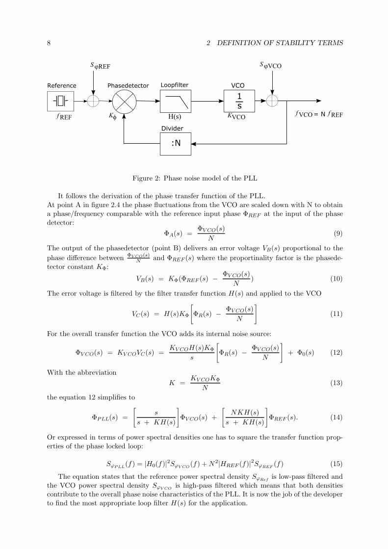
2.4 Phase noise model of a phase locked loop
A common method to generate high stable reference frequencies is to make use of a phase lockedloop (PLL). This will reduce the overall output power spectral density as derived in the previoussection. The output frequency is phase locked to a reference source at a lower frequency [2.4].The modeling of phase noise in a PLL follows the description in [2]. This model describes howthe phase noise of the reference (Sϕ REF (f)) and the VCO (Sϕ V CO(f)) are filtered by the looptransfer function. This model excludes noise sources in the Phasedetector (PD), Loop Filter(LF) and Frequency divider (N).
5Amplitude Modulation6Phase Modulation
8 2 DEFINITION OF STABILITY TERMS
Figure 2: Phase noise model of the PLL
It follows the derivation of the phase transfer function of the PLL.At point A in figure 2.4 the phase fluctuations from the VCO are scaled down with N to obtaina phase/frequency comparable with the reference input phase ΦREF at the input of the phasedetector:
ΦA(s) =ΦV CO(s)
N(9)
The output of the phasedetector (point B) delivers an error voltage VB(s) proportional to the
phase difference between ΦV CO(s)N
and ΦREF (s) where the proportinality factor is the phasede-tector constant KΦ:
VB(s) = KΦ(ΦREF (s) − ΦV CO(s)
N) (10)
The error voltage is filtered by the filter transfer function H(s) and applied to the VCO
VC(s) = H(s)KΦ
[
ΦR(s) − ΦV CO(s)
N
]
(11)
For the overall transfer function the VCO adds its internal noise source:
ΦV CO(s) = KV COVC(s) =KV COH(s)KΦ
s
[
ΦR(s) − ΦV CO(s)
N
]
+ Φ0(s) (12)
With the abbreviation
K =KV COKΦ
N(13)
the equation 12 simplifies to
ΦPLL(s) =
[
s
s + KH(s)
]
ΦV CO(s) +
[
NKH(s)
s + KH(s)
]
ΦREF (s). (14)
Or expressed in terms of power spectral densities one has to square the transfer function prop-erties of the phase locked loop:
SϕPLL(f) = |H0(f)|2SϕV CO
(f) + N2|HREF (f)|2SϕREF(f) (15)
The equation states that the reference power spectral density SϕRefis low-pass filtered and
the VCO power spectral density SϕV COis high-pass filtered which means that both densities
contribute to the overall phase noise characteristics of the PLL. It is now the job of the developerto find the most appropriate loop filter H(s) for the application.
2.5 Integrated phase noise and timing jitter 9
2.5 Integrated phase noise and timing jitter
An important figure of stability is not only the definite phase noise at offsetfrequencies of anRF source but also the integrated phase noise and the integrated timing jitter. For a measuredphasenoise characteristic Lϕ(f) the integrated phase noise can be calculated as follows:
∆φ =
√∫ f2
f1
Sϕ(f)df [rad]rms (16)
where Sϕ(f) is two times the single sideband phase noise Lϕ(f) and f1 and f2 denote thebandwidth over which the noise has to be integrated. The integrated phase noise (equation 16)can be related to the carrier f0 under consideration and give the integrated timing jitter:
∆Trms =1
2πf0
√∫ f2
f1
Sϕ(f)df [s]rms (17)
A lower integration limit f1 of 10 Hz corresponds to an error in an observation time fasterthan 100 ms. If one wishes to investigate the stability of a source within 1 second one has tointegrate from 1 Hz up to the upper frequency limit given by f2. For the stability considerationsdiscussed for the Master Oscillator in section 4 the lower limit f1 is at 10 Hz and the upper limitf2 is at 1 MHz.
2.6 Drifts
Drifts is the long term stability of an RF source and their related phases at distances rangingfrom a few meters up to hundreds of meter inside the accelerator facility. It is a measure todetermine how different frequencies generated in one source change their phase relation. Thischange of the phase is mainly caused by the change of temperature. The quantification of thesedrifts is given as a temporal variation of a carrier phase caused by temperature changes:
drifts[ sec
C
]
=∆t
∆T
[ sC
]
(18)
A temperature change of 10 C leads to an increasing change of phase expressed in portions ofthe carrier period.
10 3 MEASUREMENT PRINCIPLES
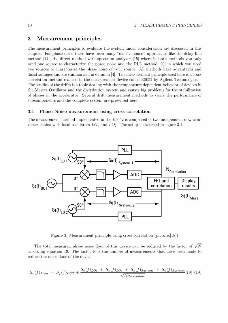
3 Measurement principles
The measurement principles to evaluate the system under consideration are discussed in thischapter. For phase noise there have been many ”old fashioned” approaches like the delay linemethod [14], the direct method with spectrum analyzer [15] where in both methods you onlyneed one source to characterize the phase noise and the PLL method [20] in which you needtwo sources to characterize the phase noise of your source. All methods have advantages anddisadvantages and are summarized in detail in [4]. The measurement principle used here is a crosscorrelation method realized in the measurement device called E5052 by Agilent Technologies.The studies of the drifts is a topic dealing with the temperature dependent behavior of devices inthe Master Oscillator and the distribution system and causes big problems for the stabilizationof phases in the accelerator. Several drift measurement methods to verify the performance ofsubcomponents and the complete system are presented here.
3.1 Phase Noise measurement using cross correlation
The measurement method implemented in the E5052 is comprised of two independent downcon-verter chains with local oscillators LO1 and LO2. The setup is sketched in figure 3.1.
ADC
FFT andcorrelation
90°
PLL
0°
ADC
90°
PLL
0°
Displayresults
Figure 3: Measurement principle using cross correlation (picture:[18])
The total measured phase noise floor of this device can be reduced by the factor of√
Naccording equation 19. The factor N is the number of measurements that have been made toreduce the noise floor of the device.
Sϕ(f)Meas = Sϕ(f)DUT +Sϕ(f)LO1
+ Sϕ(f)LO2+ Sϕ(f)System1
+ Sϕ(f)System2√NCorrelation
[19] (19)

3.2 Drift measurement methods 11
3.2 Drift measurement methods
3.2.1 Principle operation of a phasedetector
The principle measurement method to characterize drift contribution of RF sources and theelectronics behind it is based on measuring the phase variation of two RF sources. Figure 4illustrates the phasedetector that is symbolized by a common mixer symbol.
Figure 4: Phasedetector and mixer
In the case of using a double balanced mixer the inputs of the detector are the local oscillatorLO and the radio frequency RF input. In the drift measurement setup 3.2.2 the two inputshave the same frequency f0. The output voltage of the phasedetector is proportional to thephasedifference ∆φ of the two input phases φ1 of the RF and φ2 of the LO. The proportionalityfactor is called the phasedetector gain Kφ and is given in V
rador respectively V
.
The output voltage versus phasedifference of a typical phasedetector is shown in figure 5.
PHASE DIFFERENCE – Degrees
PH
AS
E O
UT
– V
–180 –150
1.80
–120 –90 –60 –30 0 30 60 90
1.62
1.44
1.26
1.08
0.90
0.72
0.54
0.36
0.00120 150 180
0.18
ER
RO
R –
De
gre
es
10
8
6
4
2
0
–2
–4
–6
–10
–8
Figure 5: Slope of AD8302 and phase error [6]
For this detector the Kφ can be found as 1.8 V180
= 10 mV
. From this plot it can also beseen that for phase differences leading to voltages at the lower corner of 0 V or the upper endof the detector 1.8 V the phase error of the detector is significantly increased. To minimize

12 3 MEASUREMENT PRINCIPLES
nonlinear distortions the operating point should be chosen such that the detector works at anoperating point from 500 mV up to 1.4 V. The operating point can be adjusted by introducinga phase shift of the RF input phase φ1 and φ2 by adjusting the cable length or by using a phaseshifter. A factor of
λeff
47 as the length difference between the two cables will not only lead to
the smallest phase errors but also gives the maximum sensitivity to detect phase variations [4].
3.2.2 Drifts of a phase detector
The phase detector AD8302 from Analog Devices is found to have the smallest drift contributionfrom commercially available phasedetectors. A measurement setup to find out the drifts of aphasedetector is sketched in figure 6.
Figure 6: Phase measurement setup
An RF source with f0 and the period T0 = 1f0
is split into two branches with the correspond-ing phases φ1 and φ2. The phase φ2 gets an additional phase shift of 90 to minimize the phaser-rors of the phasedetector. The phasedetector converts the phasedifference ∆φ = φ1 − φ2 − 90
with a conversion gain of Kφ to a proportional voltage ∆V .
∆V = Kφ ∆φ (20)
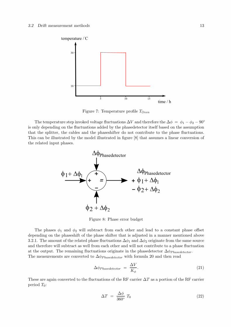
The phasedetector is put into an oven at temperature TOven with a temperature profilesketched in figure 7. The other equipment of the setup is held at constant ambient temperatureTambient.
7where λeff denotes the effective wavelength of the RF input frequency in the coaxial cable
3.2 Drift measurement methods 13
Figure 7: Temperature profile TOven
The temperature step invoked voltage fluctuations ∆V and therefore the ∆φ = φ1 − φ2 − 90
is only depending on the fluctuations added by the phasedetector itself based on the assumptionthat the splitter, the cables and the phaseshifter do not contribute to the phase fluctuations.This can be illustrated by the model illustrated in figure [8] that assumes a linear conversion ofthe related input phases.
Figure 8: Phase error budget
The phases φ1 and φ2 will subtract from each other and lead to a constant phase offsetdepending on the phaseshift of the phase shifter that is adjusted in a manner mentioned above3.2.1. The amount of the related phase fluctuations ∆φ1 and ∆φ2 originate from the same sourceand therefore will subtract as well from each other and will not contribute to a phase fluctuationat the output. The remaining fluctuations originate in the phasedetector ∆φPhasedetector.The measurements are converted to ∆φPhasedetector with formula 20 and then read
∆φPhasedetector =∆V
Kφ. (21)
These are again converted to the fluctuations of the RF carrier ∆T as a portion of the RF carrierperiod T0:
∆T =∆φ
360T0 (22)

14 3 MEASUREMENT PRINCIPLES
For a temperature step of 20 C as sketched in figure [7] the output shows fluctuations in ∆V20C
.With this procedure the inertial stability of the phasedetector is found out. For maximizingthe stability of the phase detector it has to be temperature stabilized. From the stability re-quirement of the entire Master Oscillator system in section 4.1 the accuracy requirement for thephasedetector can be estimated. As a rule of thumb it has to be at least 10 times better thanwhat is required for the whole Master Oscillator system.Evaluation measurements show [12] that a drift stability of less than 50 fs at a constant tem-perature of the phasedetector can be achieved with the AD8302.
3.2.3 Drifts of an amplifier
The drift properties of an ampifier can be characterized by using a phasedetector described inthe previous section 3.2.2. The measurement setup for measuring amplifier drifts is sketched infigure 9.
Figure 9: Drift measurement setup of an amplifier
The measurement procedure equals the description for measuring the internal phase driftsof a phasedetector. When stabilizing the phasedetector at a fixed temperature 25 C the fluc-tuations of the phasedetector are neglectible compared to the drifts of the amplifier.
3.2.4 Drifts of several RF sources
A source generating several frequencies at the same time can also be characterized concerningits drifts. The measurement setup is sketched in figure 10. A reference oscillator is a refer-ence for two equal oscillator systems generating the outputfrequencies f0, f1, f2, . . . , fn. Theoutput phases are compared with phasedetectors PD0, PD1, PD2, . . . , PDn that are stabi-lized in temperature at TOven so drift contributions from the Phasedetector are neglectible inthe range of what has been shown in section 3.2.2. Assuming that the input phases φinput 1
and φinput 2 for the two oscillators remain constant for a neglectible environmental temperaturechange a temperature step on oscillator 1 with a temperature profile Tchamber as used to char-acterize the phasedetector will give us the temperature dependence of the drifts at frequenciesf0, f1, f2, . . . , fn.

3.2 Drift measurement methods 15
Figure 10: Measurement setup to estimate drifts of two oscillator systems against each other
This setup will be used to judge the performance of the oscillator system as a whole but willnot localize the limiting electronic components inside the box.
16 4 MASTER OSCILLATOR
4 Master Oscillator
The challenging task of generating all frequencies needed in the accelerator facility with a shortterm stability of ∆T = 100 fs and a long term stability in the range of a few picosecondsis in the focus of this chapter. First an overview of the M.O. and the distribution system isgiven including a table of frequencies with required output powers. The socalled Low Powerpart (LPP), 1.3 GHz PLL, 2.856 GHz PLL, High Power Part 1.3 GHz (HPP), High Power Part81 MHz (HPP) are presented here.The phase noise performance and the related minimization of the integrated timing jitter withthe help of phase locked loops is focused on. An important issue of the PLL is its stability thatalso has been studied. A comparison of required and achieved parameters is put in the summaryof the thesis.
4.1 Overview
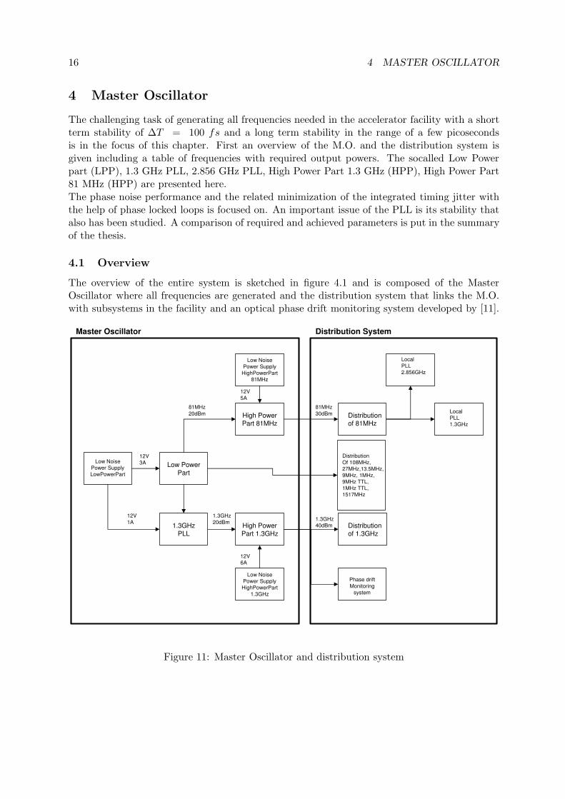
The overview of the entire system is sketched in figure 4.1 and is composed of the MasterOscillator where all frequencies are generated and the distribution system that links the M.O.with subsystems in the facility and an optical phase drift monitoring system developed by [11].
Low PowerPart
1.3GHzPLL
High PowerPart 1.3GHz
High PowerPart 81MHz
Low Noise
Power Supply
LowPowerPart
Low Noise
Power Supply
HighPowerPart
1.3GHz
Low Noise
Power Supply
HighPowerPart
81MHz
Distributionof 81MHz
Local
PLL
1.3GHz
Distribution
Of 108MHz,
27MHz,13.5MHz,
9MHz, 1MHz,
9MHz TTL,
1MHz TTL,
1517MHz
Distributionof 1.3GHz
Local
PLL
2.856GHz
12V
3A
12V
1A
12V
6A
12V
5A
81MHz
20dBm
81MHz
30dBm
1.3GHz
20dBm1.3GHz
40dBm
Phase drift
Monitoring
system
Master Oscillator Distribution System
Figure 11: Master Oscillator and distribution system

4.1 Overview 17
The frequencies required in the FLASH facility at DESY are listed in table 1:
Output frequencies [MHz] Power levels [dBm] Powers required
81.249975 (1) 19.23 2081.249975 (2) 19.47 2081.249975 (3) 19.6 20
81.249975 (4) 8 17.66 2081.249975 Monitor 0.324 0
108.3333 (1) 18.55 20108.3333 (2) 18.6 20108.3333 (3) 18.85 20
108.3333 (4) 9 16.58 20108.3333 Monitor -1.55 0
1 4.87 89.027775 (1) 21.93 209.027775 (2) 22.02 209.027775 (3) 22.03 209.027775 (4) 22.02 20
13.5416625 (1) 10.03 813.5416625 (2) 9.96 827.083325 (1) 12.27 1127.083325 (2) 12.18 11
1299.9996 19 202856.001105 15 20
81.249975 10 30 301299.9996 11 40 40
Table 1: Output powers from Master Oscillator
The requirements for the system including the distribution 12 are for the short term 100fs and for the long term 1 ps respectively [21]. The short term is defined for an integrationbandwidth from 10 Hz. . . 1 MHz and is specified in terms of phase noise for three differentfrequencies also found in the specification [21]. A comparison of phase noise characteristics willbe made when discussing the single modules in the M.O. in the following.
8goes through two couplers9goes through two couplers
10after amplification by HPP 81 MHz11after amplification by HPP 1300 MHz12not considered here
18 4 MASTER OSCILLATOR
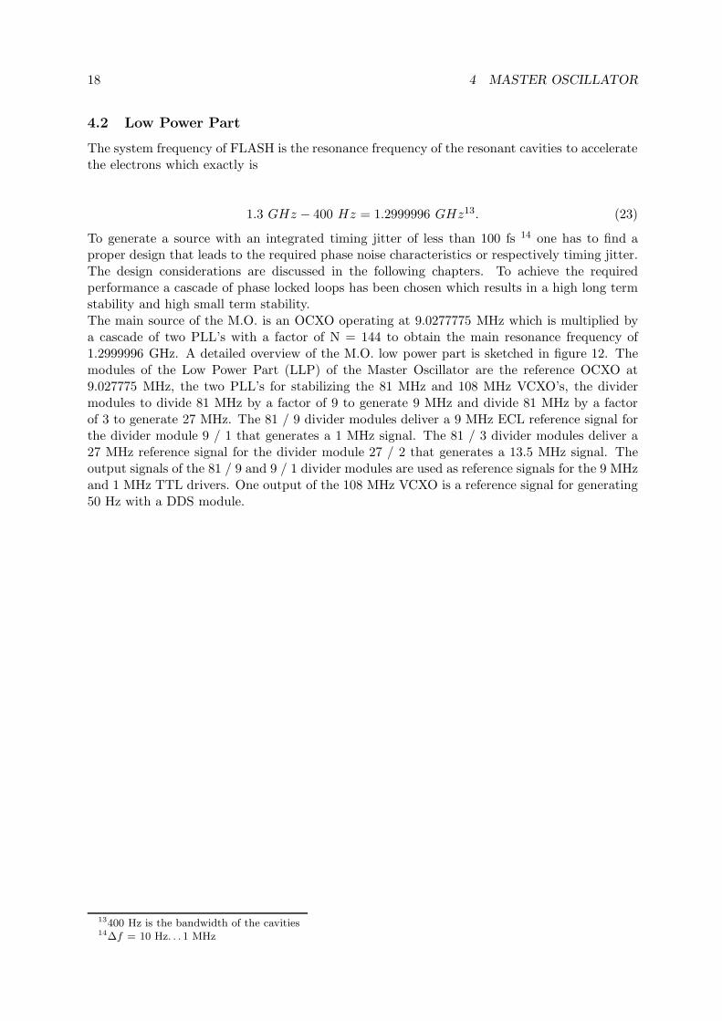
4.2 Low Power Part
The system frequency of FLASH is the resonance frequency of the resonant cavities to acceleratethe electrons which exactly is
1.3 GHz − 400 Hz = 1.2999996 GHz13. (23)
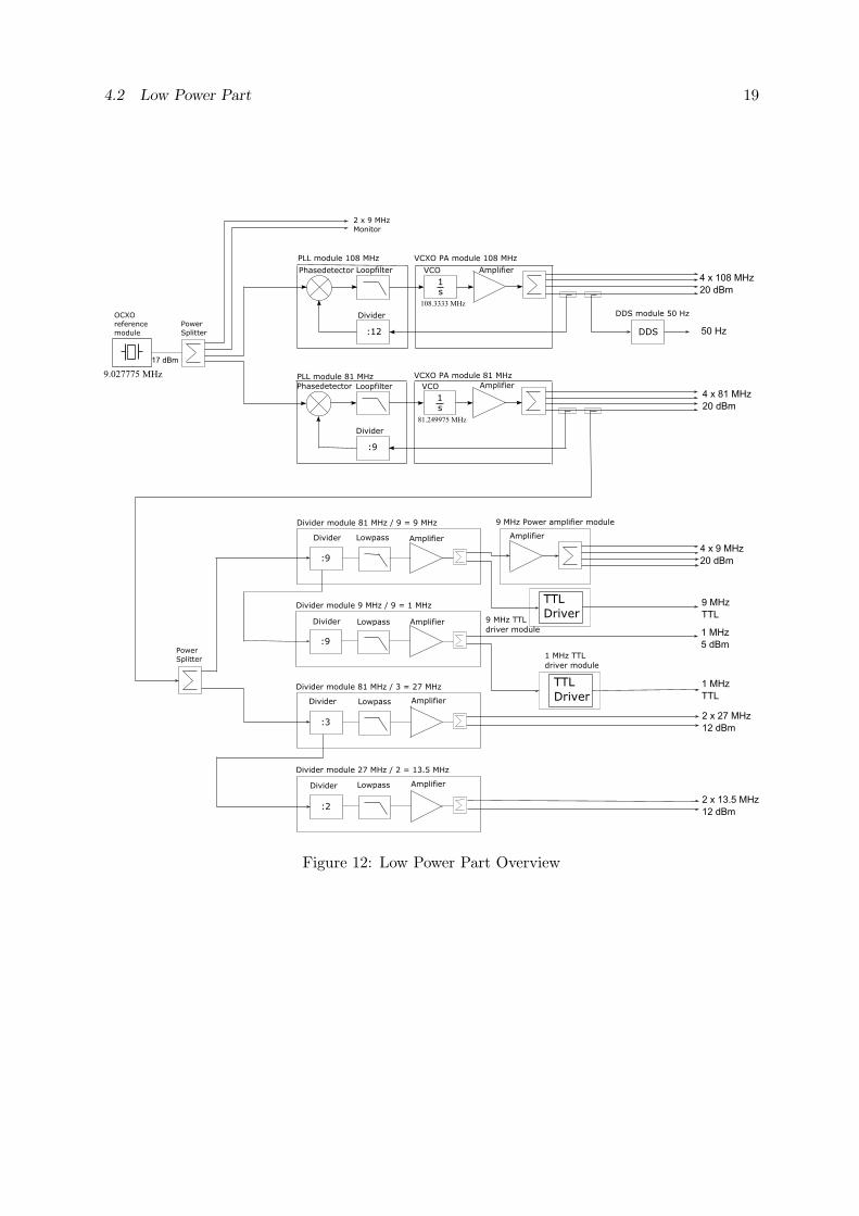
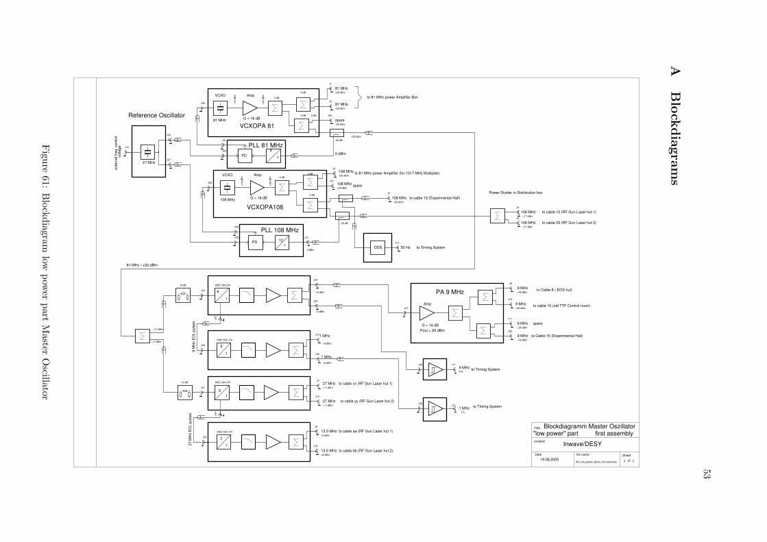
To generate a source with an integrated timing jitter of less than 100 fs 14 one has to find aproper design that leads to the required phase noise characteristics or respectively timing jitter.The design considerations are discussed in the following chapters. To achieve the requiredperformance a cascade of phase locked loops has been chosen which results in a high long termstability and high small term stability.The main source of the M.O. is an OCXO operating at 9.0277775 MHz which is multiplied bya cascade of two PLL’s with a factor of N = 144 to obtain the main resonance frequency of1.2999996 GHz. A detailed overview of the M.O. low power part is sketched in figure 12. Themodules of the Low Power Part (LLP) of the Master Oscillator are the reference OCXO at9.027775 MHz, the two PLL’s for stabilizing the 81 MHz and 108 MHz VCXO’s, the dividermodules to divide 81 MHz by a factor of 9 to generate 9 MHz and divide 81 MHz by a factorof 3 to generate 27 MHz. The 81 / 9 divider modules deliver a 9 MHz ECL reference signal forthe divider module 9 / 1 that generates a 1 MHz signal. The 81 / 3 divider modules deliver a27 MHz reference signal for the divider module 27 / 2 that generates a 13.5 MHz signal. Theoutput signals of the 81 / 9 and 9 / 1 divider modules are used as reference signals for the 9 MHzand 1 MHz TTL drivers. One output of the 108 MHz VCXO is a reference signal for generating50 Hz with a DDS module.
13400 Hz is the bandwidth of the cavities14∆f = 10 Hz. . . 1 MHz
4.2 Low Power Part 19
Figure 12: Low Power Part Overview
20 4 MASTER OSCILLATOR
4.2.1 OCXO reference module
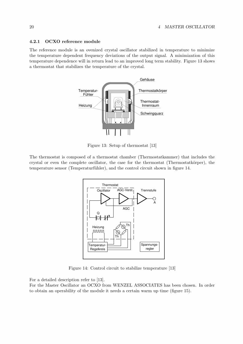
The reference module is an ovenized crystal oscillator stabilized in temperature to minimizethe temperature dependent frequency deviations of the output signal. A minimization of thistemperature dependence will in return lead to an improved long term stability. Figure 13 showsa thermostat that stabilizes the temperature of the crystal.
Gehäuse
Thermostatkörper
Thermostat-InnenraumHeizung
Temperatur-Fühler
Schwingquarz
Figure 13: Setup of thermostat [13]
The thermostat is composed of a thermostat chamber (Thermostatkammer) that includes thecrystal or even the complete oscillator, the case for the thermostat (Thermostatkorper), thetemperature sensor (Temperaturfuhler), and the control circuit shown in figure 14.
Oszillator AGC-Verst. Trennstufe
AGC
Q
A
Thermostat
Temperatur-
Regelkreis
Spannungs-
regler
Th
Th
Heizung
Bild 5.17 Thermostat,
Figure 14: Control circuit to stabilize temperature [13]
For a detailed description refer to [13].For the Master Oscillator an OCXO from WENZEL ASSOCIATES has been chosen. In orderto obtain an operability of the module it needs a certain warm up time (figure 15).

4.2 Low Power Part 21
9.02778
9.02776
9.02774
9.02772
9.02770
9.02768
9.02766
9.02764
fred
quen
cy [M
Hz]
03:0001.01.1904
06:00 09:00
time [min]
400
350
300
250
200
current I [mA
]
Figure 15: Warm up of OCXO and current consumption, Vtune = 5 V
After warm up time the module can operate at its nominal frequency f = 9.027775 MHzwith a tuning voltage of Vtune = 5V . The temperature stability after 10 minutes warmup dueto datasheet [3] is ∆f
f= 10−8. The aging after 30 days of operation is 10−9. The module
can also be detuned by a tuning voltage Vtune = 5V in its frequency to correct for potentialdeviation of the reference frequency after a long operating time or also in order to synchronizeto an external reference source. The tuning voltage ranges from 0 V < Vtune < 10 V . Thefrequency dependence of the tuning voltage is sketched in figure 16. The tuning sensitivity isKV CO = 5 Hz
V.

22 4 MASTER OSCILLATOR
9.02779
9.02778
9.02777
9.02776
9.02775
freq
uenc
y [M
Hz]
1086420tuning voltage [V]
Figure 16: Tuning slope of reference module
The short term stability is specified in terms of phase noise and the datasheet values from theOCXO module are listed in table 2.
offsetfrequency [Hz] SSB Phasenoise [dBc/Hz]
1 -10510 -135100 -1501000 -15510000 -162100000 -1641000000 -164
Table 2: Phase noise reference module
The phase noise contribution of the reference to the various ouputs will be considered in thefollowing section 4.2.2.
4.2.2 The 81 MHz and 108 MHz phase locked loops
The phase locked loops for 81 MHz and 108 MHz are composed of the reference OCXO at9.027775 MHz, a phasedetector, a loopfilter and a frequency divider and of the VCXO’s at 81MHz and 108 MHz respectively (figure 17).

4.2 Low Power Part 23
Figure 17: Phase locked loop for 81 MHz and 108 MHz VCXO’s
The VCXO modules contain a fifth overtone tunable crystal oscillators with very low phase noisecharacteristics and an additional amplifier to deliver the required output power. The outputamplifier is inside the loop so drifts of the amplifier will be compensated for. The closed looptransfer function reads
GCL(s) =GOL(s)
(
1 + GOL(s)n
) , (24)
where N is the division ratio in the feedback of the phase locked loop and GOL is the open looptransfer function that reads
GOL(s) =Kφ KV CO HLF (s)
s, (25)
with loop parameters Kφ the phasedetector constant, KV CO the voltage controlled oscillatorgain and HLF (s) the loopfilter transferfunction that will be discussed later.
The phasedetector and frequency divider:
The phasedetector and frequency divider are combined in one integrated circuit HMC440 fromHittite [10]. The phasedetector has a differential output ND and NU and the frequency divideris programmable with values from 1 to 32. For the 81 MHz PLL a division factor of N = 9and for the 108 MHz PLL a factor of N = 12 is chosen to obtain in both cases a comparisonfrequency of 9.027775 MHz.The phasedetector will add its internal residual phase noise what is not considered in the modelintroduced in section 2.4. A phasedetector that shows significantly worse phase noise charac-teristics as compared to the reference OCXO at the 9.027775 MHz input signal would limitthe minimum phase noise transport through the PLL. The phasenoise of the phasedetctor issketched in figure 18.
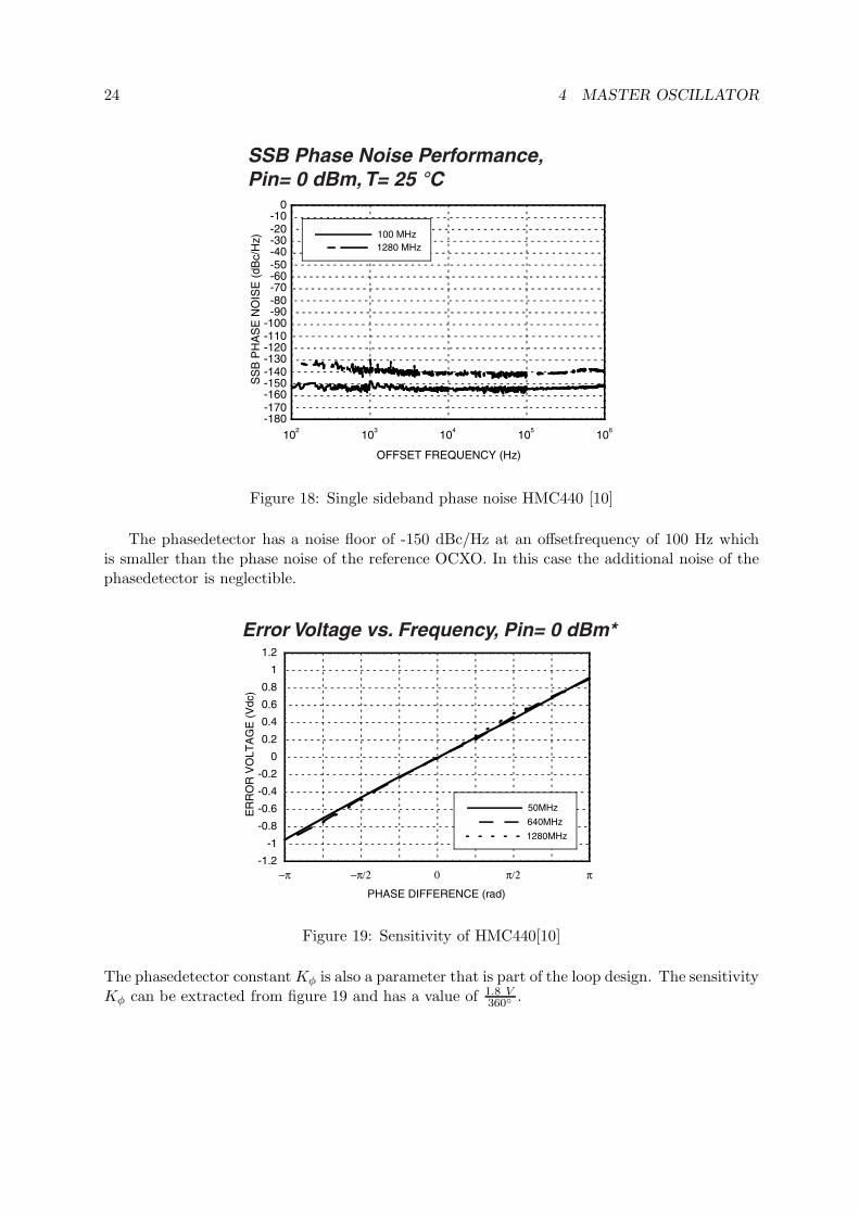
24 4 MASTER OSCILLATOR
SSB Phase Noise Performance,
Pin= 0 dBm, T= 25 °C
-180-170-160-150-140-130-120-110-100-90-80-70-60-50-40-30-20-10
0
102
103
104
105
106
100 MHz
1280 MHzS
SB
PH
AS
E N
OIS
E (
dB
c/H
z)
OFFSET FREQUENCY (Hz)
Figure 18: Single sideband phase noise HMC440 [10]
The phasedetector has a noise floor of -150 dBc/Hz at an offsetfrequency of 100 Hz whichis smaller than the phase noise of the reference OCXO. In this case the additional noise of thephasedetector is neglectible.
GaAs MMIC SUB-HARMONICALError Voltage vs. Frequency, Pin= 0 dBm*
-1.2
-1
-0.8
-0.6
-0.4
-0.2
0
0.2
0.4
0.6
0.8
1
1.2
−π −π/2 0 π/2 π
50MHz
640MHz
1280MHz
ER
RO
R V
OLT
AG
E (
Vdc)
PHASE DIFFERENCE (rad)
Figure 19: Sensitivity of HMC440[10]
The phasedetector constant Kφ is also a parameter that is part of the loop design. The sensitivityKφ can be extracted from figure 19 and has a value of 1.8 V
360 .
4.2 Low Power Part 25
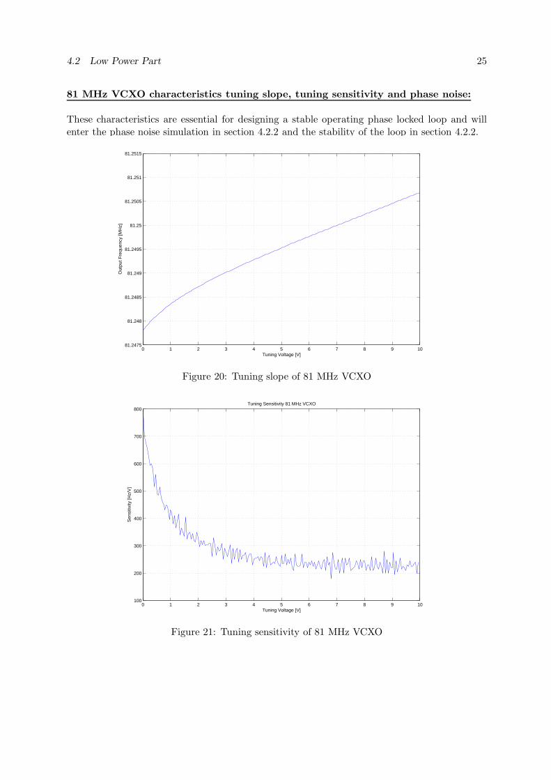
81 MHz VCXO characteristics tuning slope, tuning sensitivity and phase noise:
These characteristics are essential for designing a stable operating phase locked loop and willenter the phase noise simulation in section 4.2.2 and the stability of the loop in section 4.2.2.
0 1 2 3 4 5 6 7 8 9 1081.2475
81.248
81.2485
81.249
81.2495
81.25
81.2505
81.251
81.2515
Tuning Voltage [V]
Out
put F
requ
ency
[MH
z]
Figure 20: Tuning slope of 81 MHz VCXO
0 1 2 3 4 5 6 7 8 9 10100
200
300
400
500
600
700
800
Tuning Voltage [V]
Sen
sitiv
ity [H
z/V
]
Tuning Sensitivity 81 MHz VCXO
Figure 21: Tuning sensitivity of 81 MHz VCXO

26 4 MASTER OSCILLATOR
100
101
102
103
104
105
106
107
−180
−160
−140
−120
−100
−80
−60
Offsetfrequency [Hz]
Pha
se N
oise
[dB
c/H
z]
Figure 22: Phase noise of freerunning 81 MHz VCXO
108 MHz VCXO characteristics tuning slope, tuning sensitivity and phase noise:
0 1 2 3 4 5 6 7 8 9 10108.33
108.332
108.334
108.336
108.338
108.34
108.342
108.344
Tuning Voltage [V]
Out
put F
requ
ency
[MH
z]
Figure 23: Tuning slope of 108 MHz VCXO
4.2 Low Power Part 27
0 1 2 3 4 5 6 7 8 9 100
500
1000
1500
2000
2500
Tuning Voltage [V]
Sen
sitiv
ity [H
z/V
]
Tuning Sensitivity 108 MHz VCXO
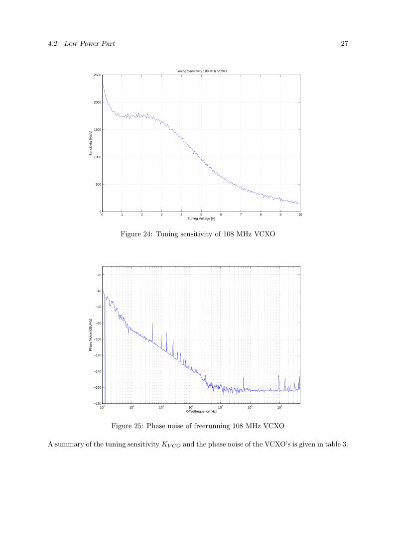
Figure 24: Tuning sensitivity of 108 MHz VCXO
100
101
102
103
104
105
106
−180
−160
−140
−120
−100
−80
−60
−40
−20
Offsetfrequency [Hz]
Pha
se N
oise
[dB
c/H
z]
Figure 25: Phase noise of freerunning 108 MHz VCXO
A summary of the tuning sensitivity KV CO and the phase noise of the VCXO’s is given in table 3.
28 4 MASTER OSCILLATOR
81 MHz VCXO 108 MHz VCXO
KV CO 250 Hz/V 15 1.75 kHz/V 16
10 -95 -88100 -120 -1051000 -148 -13510000 -163 -160100000 -165 -163
Table 3: VCXO parameters
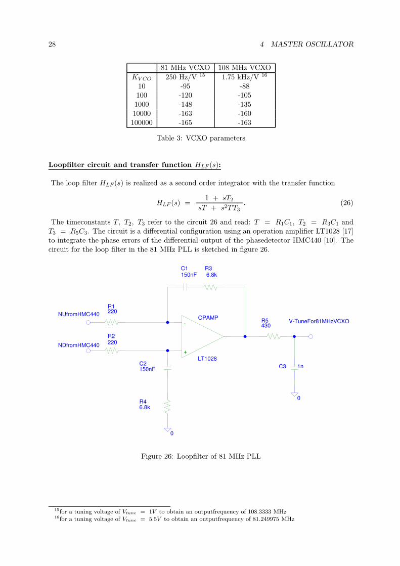
Loopfilter circuit and transfer function HLF (s):
The loop filter HLF (s) is realized as a second order integrator with the transfer function
HLF (s) =1 + sT2
sT + s2TT3. (26)
The timeconstants T, T2, T3 refer to the circuit 26 and read: T = R1C1, T2 = R3C1 andT3 = R5C3. The circuit is a differential configuration using an operation amplifier LT1028 [17]to integrate the phase errors of the differential output of the phasedetector HMC440 [10]. Thecircuit for the loop filter in the 81 MHz PLL is sketched in figure 26.
R1220
220R2
C1150nF
R36.8k
R46.8k
+
-OPAMP
LT1028
R5430
1nC3C2150nF
0
NUfromHMC440
NDfromHMC440
0
V-TuneFor81MHzVCXO
Figure 26: Loopfilter of 81 MHz PLL
15for a tuning voltage of Vtune = 1V to obtain an outputfrequency of 108.3333 MHz16for a tuning voltage of Vtune = 5.5V to obtain an outputfrequency of 81.249975 MHz
4.2 Low Power Part 29
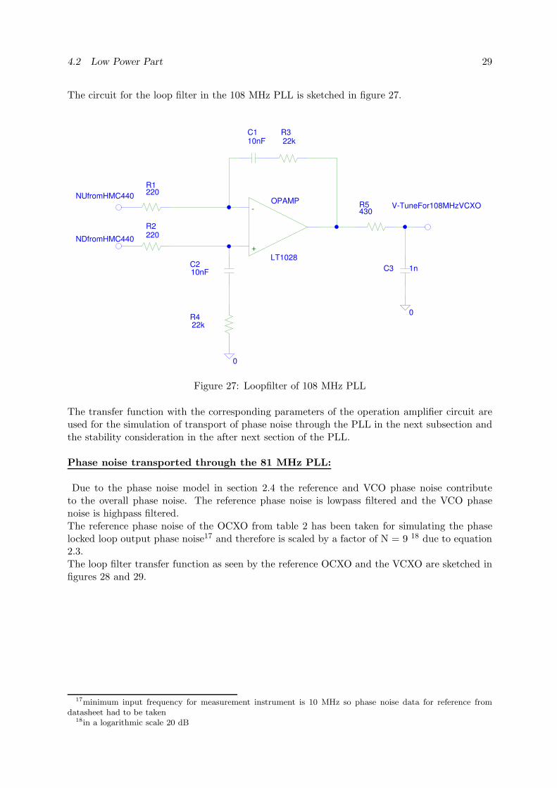
The circuit for the loop filter in the 108 MHz PLL is sketched in figure 27.
R1220
220R2
+
-OPAMP
LT1028
R5430
1nC3
10nFC1
10nFC2
22kR3
22kR4
0
NUfromHMC440
NDfromHMC440
0
V-TuneFor108MHzVCXO
Figure 27: Loopfilter of 108 MHz PLL
The transfer function with the corresponding parameters of the operation amplifier circuit areused for the simulation of transport of phase noise through the PLL in the next subsection andthe stability consideration in the after next section of the PLL.
Phase noise transported through the 81 MHz PLL:
Due to the phase noise model in section 2.4 the reference and VCO phase noise contributeto the overall phase noise. The reference phase noise is lowpass filtered and the VCO phasenoise is highpass filtered.The reference phase noise of the OCXO from table 2 has been taken for simulating the phaselocked loop output phase noise17 and therefore is scaled by a factor of N = 9 18 due to equation2.3.The loop filter transfer function as seen by the reference OCXO and the VCXO are sketched infigures 28 and 29.
17minimum input frequency for measurement instrument is 10 MHz so phase noise data for reference fromdatasheet had to be taken
18in a logarithmic scale 20 dB

30 4 MASTER OSCILLATOR
100
101
102
103
104
105
106
107
−1
−0.5
0
0.5
1
1.5
2
offsetfrequency [Hz]
mag
nitu
de [a
.u.]
lowpass filter for referencehighpass filter for VCXO
Figure 28: Lowpass as ”seen” by the 9.027775 MHz OCXO reference and highpass filtered asseen by the 81 MHz VCXO
The loop filter as simulated shows a cutoff at around 100 Hz what could be verified by themeasurement of phase noise of the closed loop 81 MHz VCXO as depicted in figure 29.
100
101
102
103
104
105
106
107
−180
−160
−140
−120
−100
−80
−60
−40
offsetfrequency [Hz]
phas
enoi
se [d
Bc/
Hz]
scaled reference phasenoisefiltered VCO phasenoisemeasured phasenoise of locked VCXO
Figure 29: 81 MHz phase locked loop with highpass filtered 81 MHz VCXO phase noise
The scaled reference phase noise deviates by roughly 10 dB up to 15 dB from measurementsof closed loop phase noise. A discussion of deviations will be given in the summary. Theintegrated timing jitter19 for measured phase noise at 81 MHz is around 70 fs20.
1910 Hz. . . 1 MHz20measured without correlation
4.2 Low Power Part 31
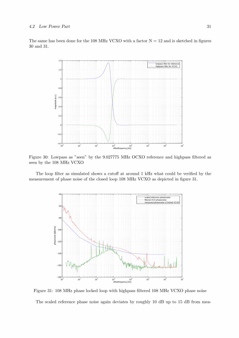
The same has been done for the 108 MHz VCXO with a factor N = 12 and is sketched in figures30 and 31.
100
101
102
103
104
105
106
107
−0.4
−0.2
0
0.2
0.4
0.6
0.8
1
1.2
1.4
offsetfrequency [Hz]
mag
nitu
de [a
.u.]
lowpass filter for referencehighpass filter for VCXO
Figure 30: Lowpass as ”seen” by the 9.027775 MHz OCXO reference and highpass filtered asseen by the 108 MHz VCXO
The loop filter as simulated shows a cutoff at around 1 kHz what could be verified by themeasurement of phase noise of the closed loop 108 MHz VCXO as depicted in figure 31.
100
101
102
103
104
105
106
107
−180
−160
−140
−120
−100
−80
−60
−40
offsetfrequency [Hz]
phas
enoi
se [d
Bc/
Hz]
scaled reference phasenoisefiltered VCO phasenoisemeasured phasenoise of locked VCXO
Figure 31: 108 MHz phase locked loop with highpass filtered 108 MHz VCXO phase noise
The scaled reference phase noise again deviates by roughly 10 dB up to 15 dB from mea-

32 4 MASTER OSCILLATOR
surements of closed loop phase noise. The integrated timing jitter21 for measured phase noiseat 81 MHz is around 75 fs22.
Stability of loops:
The stability limit for control loops such as phase locked loops is when the open loop gainGOL > 1 when the phase shift of the open loop reaches φ = −180.
This means that phase errors will no longer be subtracted but added in the feedback of acontrol loop due to the change of sign introduced by the phaseshift bigger than φ = −180.Amplitude and phase of open loop transfer functions of the phase locked loops for 81 MHz and108 MHz have been simulated. The results are shown in figure 32 for the 81 MHz loop and infigure 33 for the 108 MHz loop respectively.
−150
−100
−50
0
50
100
150
Mag
nitu
de (
dB)
101
102
103
104
105
106
107
108
−180
−135
−90
Pha
se (
deg)
Bode Diagram
Frequency (rad/sec)
Figure 32: Magnitude and phase of closed loop transfer function of 81 MHz PLL
2110 Hz. . . 1 MHz22measured without correlation

4.2 Low Power Part 33
−100
−50
0
50
100
150M
agni
tude
(dB
)
102
103
104
105
106
107
108
−180
−135
−90
Pha
se (
deg)
Bode Diagram
Frequency (rad/sec)
Figure 33: Magnitude and phase of closed loop transfer function of 108 MHz PLL
Both loops are stable and have a phasemargin φmargin > 60 23.
Harmonics at the output of 81 MHz and 108 MHz loop:
The harmonics of the outputs at 81 MHz and 108 MHz are measured with a spectrum ana-lyzer. The requirement document [21] requires a distance of harmonics < 25 dB below thecarrier. A summary of harmonic distance in the outputs is given in table 63.
fundamental 1st harmonic [dBc] 2nd harmonic [dBc] 3rd harmonic [dBc]
81MHz <35 <40 <40108MHz <35 <35 n.m.24
Table 4: Table of harmonics in outputs from locked 81 MHz and 108 MHz VCXO
23point at which the gain decreased to |G| = |1|24n.m.= not measured

34 4 MASTER OSCILLATOR
Att 40 dBRef 10 dBm
Center 250 MHz Span 500 MHz50 MHz/
*RBW 30 kHz
VBW 100 kHz
SWT 560 ms
P
-90
-80
-70
-60
-50
-40
-30
-20
-10
0
10
1
Marker 1 [T1 ]
0.17 dBm
81.000000000 MHz
2
Marker 2 [T1 ]
-37.61 dBm
162.000000000 MHz
3
Marker 3 [T1 ]
-40.59 dBm
244.000000000 MHz
4
Marker 4 [T1 ]
-43.34 dBm
325.000000000 MHz
Figure 34: Harmonic content of 81 MHz output
Att 40 dBRef 10 dBm
Center 250 MHz Span 500 MHz50 MHz/
*RBW 30 kHz
VBW 100 kHz
SWT 560 ms
P
-90
-80
-70
-60
-50
-40
-30
-20
-10
0
10
1
Marker 1 [T1 ]
-2.07 dBm
108.000000000 MHz
2
Marker 2 [T1 ]
-37.22 dBm
325.000000000 MHz
3
Marker 3 [T1 ]
-37.34 dBm
217.000000000 MHz
Figure 35: Harmonic content of 108 MHz output

4.2 Low Power Part 35
4.2.3 Divider modules for 27 MHz, 13.5 MHz, 9 MHz, 1 MHz
The divider modules that generate the frequencies 27 MHz, 13.5 MHz, 9 MHz and 1 MHzare programmable with division factors from 0 to 32. The chip used here is the HMC394 [9].The divider is a device based on ECL technology that features two independent outputs of thedivided signal. One signal is low pass filtered and amplified to deliver the powers listed in table1. The other output is inverted and serves as a reference signal for the other module as sketchedin figure 12. The phase noise limits of the chip are sketched in figure 36.
-160
-150
-140
-130
-120
-110
-100
-90
-80
-70
-60
102
103
104
105
106
107
SS
B P
HA
SE
NO
ISE
(dB
c/H
z)
OFFSET FREQUENCY (Hz)
SSB Phase Noise Performance,
Fin= 1 GHz, N= 4, T= 25 °C
Figure 36: Phase noise floor of divider module [9]
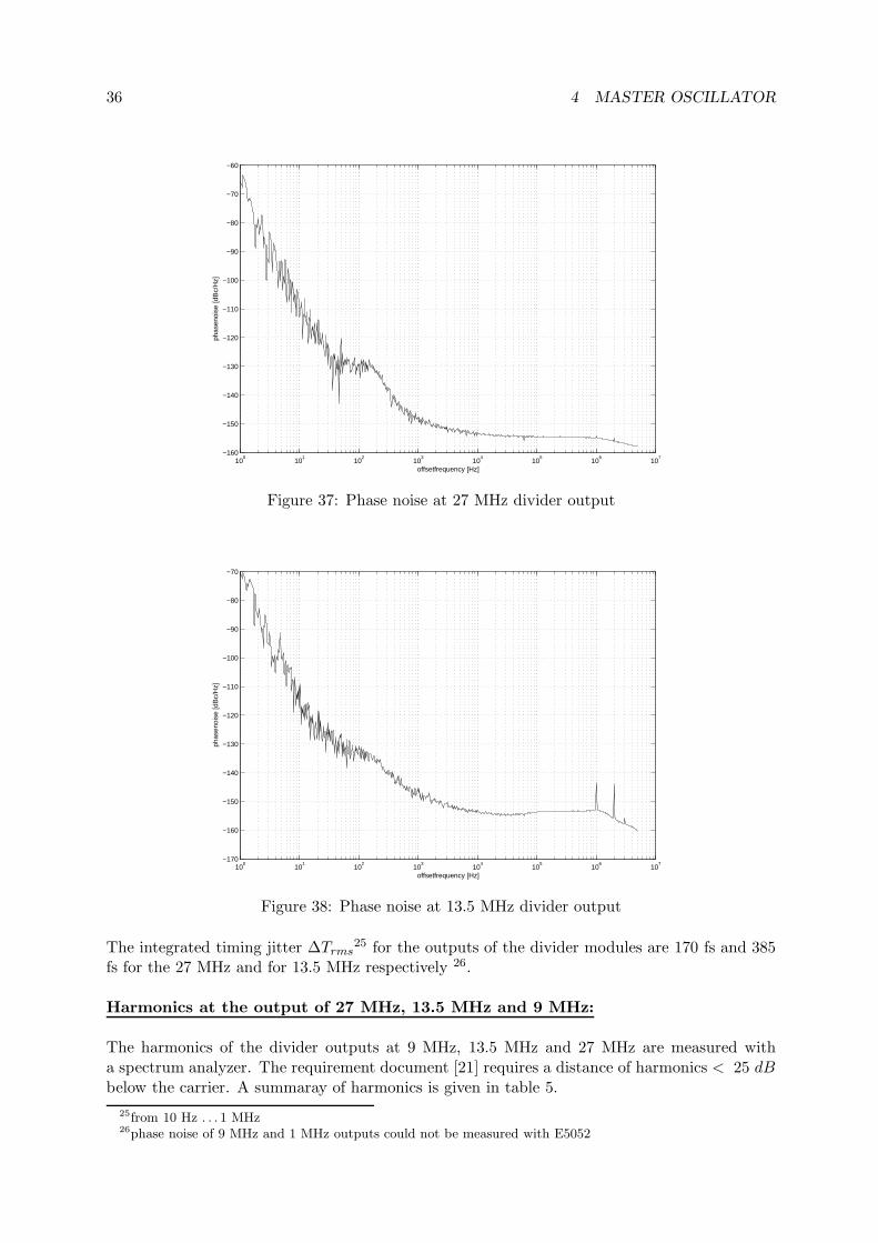
The phase noise at offsetfrequency 100 Hz is -140 dBc/Hz, at 1 kHz -150 dBc/Hz and a phasenoise floor of -155 dBc/Hz is reached at 10 kHz offset frequency. The phase noise of the outputs27 MHz and 13.5 MHz is sketched in figure 37 and 38.
36 4 MASTER OSCILLATOR
100
101
102
103
104
105
106
107
−160
−150
−140
−130
−120
−110
−100
−90
−80
−70
−60
offsetfrequency [Hz]
phas
enoi
se [d
Bc/
Hz]
Figure 37: Phase noise at 27 MHz divider output
100
101
102
103
104
105
106
107
−170
−160
−150
−140
−130
−120
−110
−100
−90
−80
−70
offsetfrequency [Hz]
phas
enoi
se [d
Bc/
Hz]
Figure 38: Phase noise at 13.5 MHz divider output
The integrated timing jitter ∆Trms25 for the outputs of the divider modules are 170 fs and 385
fs for the 27 MHz and for 13.5 MHz respectively 26.
Harmonics at the output of 27 MHz, 13.5 MHz and 9 MHz:
The harmonics of the divider outputs at 9 MHz, 13.5 MHz and 27 MHz are measured witha spectrum analyzer. The requirement document [21] requires a distance of harmonics < 25 dBbelow the carrier. A summaray of harmonics is given in table 5.
25from 10 Hz . . . 1 MHz26phase noise of 9 MHz and 1 MHz outputs could not be measured with E5052

4.2 Low Power Part 37
fundamental 1st harmonic [dBc] 2nd harmonic [dBc] 3rd harmonic [dBc]
9MHz <40 <60 <7013.5MHz <45 n.m.27 n.m.27MHz <50 n.m. n.m.
Table 5: Table of harmonics in 9 MHz, 13.5 MHz and 27 MHz divider module
4.2.4 9 MHz Power amplifier
The output of the 81 MHz / 9 divider module is amplified again to obtain four outputs withapproximately 20 dBm for each output. The output versus input power characteristic of one ofthe four outputs is sketched in figure 39.
20
15
10
5
0
-5
Out
put P
ower
[dB
m]
-25 -20 -15 -10 -5 0Input Power [dBm]
1dB compression point Old Design 9MHz PA Ideal Old PA
Figure 39: 1 dB compression point of 9 MHz module
An operation in the linear regime of the amplifier is recommended and minimizes the phasedeviation from the input to the output. An input power of 0 dBm is sufficient to deliver anoutput power of approximately 20 dBm for each output.
4.2.5 TTL drivers for 9 MHz and 1 MHz TTL signal
For timing purposes in the facility two outputs with TTL signal levels at 9 MHz and 1 MHz arerequired [21]. The TTL driver input and output signals are sketched in figures 40 and 41. Theinput signals are delivered from the divider modules.
27n.m. = not measured

38 4 MASTER OSCILLATOR
-1.0
-0.5
0.0
0.5
1.0S
IN a
mpl
itude
[V]
0.20.10.0-0.1-0.2time [us]
4
3
2
1
0
TT
L amplitude [V
]
sin9MHz_amplitude ttl9M_amplitude
Figure 40: 9 MHz sinusoidal input - and TTL output signal
-0.4
-0.2
0.0
0.2
0.4
SIN
am
plitu
de [
V]
-2 -1 0 1 2time [us]
4
3
2
1
0
TT
L amplitude [V
]
sinusoidal input signal 1 MHz TTL output signal
Figure 41: 1 MHz sinusoidal input - and TTL output signal
The additional jitter of these drivers have not been investigated up to this point.
4.2.6 Direct digital synthesis of 50 Hz
The input signal for the DDS module is coupled out from the 108 MHz VCXO module andgenerates the signal sketched in figure 42.
4.3 1.3 GHz and 2.856 GHz phase locked loops 39
1.6
1.4
1.2
1.0
0.8
0.6
0.4
0.2
0.0
am
plit
ude [V
]
100500-50-100
time [ms]
Figure 42: Output signal 50 Hz DDS
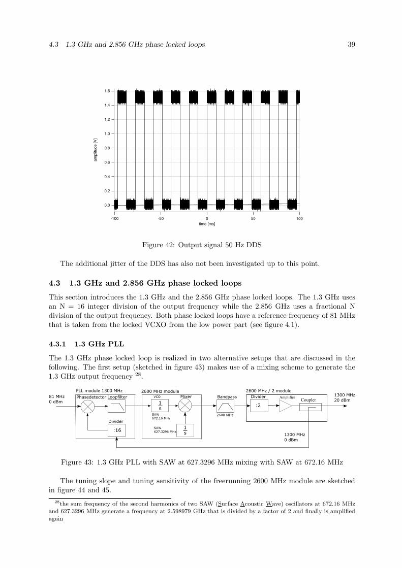
The additional jitter of the DDS has also not been investigated up to this point.
4.3 1.3 GHz and 2.856 GHz phase locked loops
This section introduces the 1.3 GHz and the 2.856 GHz phase locked loops. The 1.3 GHz usesan N = 16 integer division of the output frequency while the 2.856 GHz uses a fractional Ndivision of the output frequency. Both phase locked loops have a reference frequency of 81 MHzthat is taken from the locked VCXO from the low power part (see figure 4.1).
4.3.1 1.3 GHz PLL
The 1.3 GHz phase locked loop is realized in two alternative setups that are discussed in thefollowing. The first setup (sketched in figure 43) makes use of a mixing scheme to generate the1.3 GHz output frequency 28.
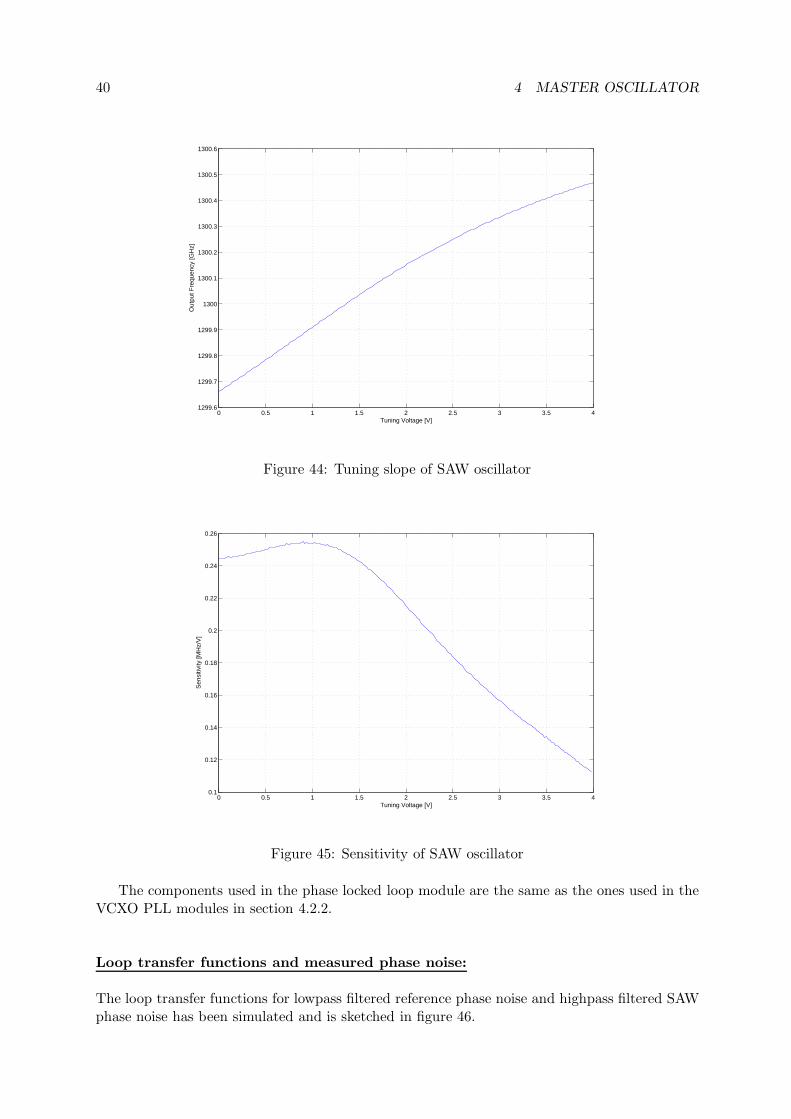
Figure 43: 1.3 GHz PLL with SAW at 627.3296 MHz mixing with SAW at 672.16 MHz
The tuning slope and tuning sensitivity of the freerunning 2600 MHz module are sketchedin figure 44 and 45.
28the sum frequency of the second harmonics of two SAW (Surface Acoustic Wave) oscillators at 672.16 MHzand 627.3296 MHz generate a frequency at 2.598979 GHz that is divided by a factor of 2 and finally is amplifiedagain
40 4 MASTER OSCILLATOR
0 0.5 1 1.5 2 2.5 3 3.5 41299.6
1299.7
1299.8
1299.9
1300
1300.1
1300.2
1300.3
1300.4
1300.5
1300.6
Tuning Voltage [V]
Out
put F
requ
ency
[GH
z]
Figure 44: Tuning slope of SAW oscillator
0 0.5 1 1.5 2 2.5 3 3.5 40.1
0.12
0.14
0.16
0.18
0.2
0.22
0.24
0.26
Tuning Voltage [V]
Sen
sitiv
ity [M
Hz/
V]
Figure 45: Sensitivity of SAW oscillator
The components used in the phase locked loop module are the same as the ones used in theVCXO PLL modules in section 4.2.2.
Loop transfer functions and measured phase noise:
The loop transfer functions for lowpass filtered reference phase noise and highpass filtered SAWphase noise has been simulated and is sketched in figure 46.

4.3 1.3 GHz and 2.856 GHz phase locked loops 41
100
101
102
103
104
105
106
107
−0.4
−0.2
0
0.2
0.4
0.6
0.8
1
1.2
1.4
offsetfrequency [Hz]
mag
nitu
de [a
.u.]
lowpass filter for reference
highpass filter for SAW
Figure 46: Transfer functions as ”seen” by the reference and the SAW
The filter shows a cut off at around 11 kHz what could be verified by measurements of theclosed loop phase noise what is sketched in figure 47. For the loop filter parameter estimationthe reference phase noise of the locked 81 MHz VCXO has been scaled by a factor of N = 16 29,the phase noise of the freerunning SAW oscillator, the simulated locked loop phase noise andthe measured locked loop phase noise are sketched in figure 47.
100
101
102
103
104
105
106
107
−160
−140
−120
−100
−80
−60
−40
−20
0
20
offsetfrequency [Hz]
phas
enoi
se [d
Bc/
Hz]
SAW freerunning 1300 MHzscaled Reference 81 MHzsimulation Sphimeasured locked PLL
Figure 47: Measured and simulated phase noise in locked SAW phase locked loop
The integrated timing jitter30 is 70 fs.
29roughly 24 dB30integration bandwidth from 10 Hz. . . 1MHz
42 4 MASTER OSCILLATOR
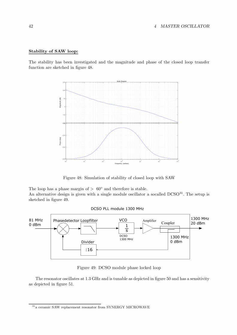
Stability of SAW loop:
The stability has been investigated and the magnitude and phase of the closed loop transferfunction are sketched in figure 48.
−100
−50
0
50
100
150
Mag
nitu
de (
dB)
103
104
105
106
107
108
109
−180
−150
−120
−90
Pha
se (
deg)
Bode Diagram
Frequency (rad/sec)
Figure 48: Simulation of stability of closed loop with SAW
The loop has a phase margin of > 60 and therefore is stable.An alternative design is given with a single module oscillator a socalled DCSO31. The setup issketched in figure 49.
Figure 49: DCSO module phase locked loop
The resonator oscillates at 1.3 GHz and is tunable as depicted in figure 50 and has a sensitivityas depicted in figure 51.
31a ceramic SAW replacement resonator from SYNERGY MICROWAVE

4.3 1.3 GHz and 2.856 GHz phase locked loops 43
0 0.5 1 1.5 2 2.5 3 3.5 4 4.5 51.296
1.297
1.298
1.299
1.3
1.301
1.302
1.303
1.304
1.305
Tuning Voltage [V]
Out
put F
requ
ency
[GH
z]
Figure 50: DCSO slope
0 0.5 1 1.5 2 2.5 3 3.5 4 4.5 51
1.2
1.4
1.6
1.8
2
2.2
2.4
2.6
2.8
Tuning Voltage [V]
Sen
sitiv
ity [M
Hz/
V]
Figure 51: Sensitivity of DCSO
Loop transfer functions and measured phase noise:
The loop transfer functions for lowpass filtered reference phase noise and highpass filtered DCSOphase noise has been simulated and is sketched in figure 52.
44 4 MASTER OSCILLATOR
100
101
102
103
104
105
106
107
−0.2
0
0.2
0.4
0.6
0.8
1
1.2
offsetfrequency [Hz]
mag
nitu
de [a
.u.]
lowpass filter for referencehighpass filter for SAW
Figure 52: Transfer functions as ”seen” by the reference and the DCSO
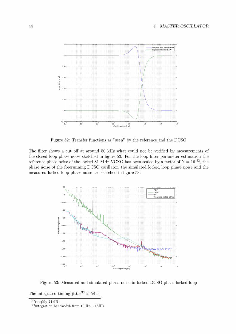
The filter shows a cut off at around 50 kHz what could not be verified by measurements ofthe closed loop phase noise sketched in figure 53. For the loop filter parameter estimation thereference phase noise of the locked 81 MHz VCXO has been scaled by a factor of N = 16 32, thephase noise of the freerunning DCSO oscillator, the simulated locked loop phase noise and themeasured locked loop phase noise are sketched in figure 53.
100
101
102
103
104
105
106
107
−180
−160
−140
−120
−100
−80
−60
−40
−20
0
20
offsetfrequency [Hz]
phas
e no
ise
[dB
c/H
z]
REFDCSOSIMmeasured locked DCSO
Figure 53: Measured and simulated phase noise in locked DCSO phase locked loop
The integrated timing jitter33 is 58 fs.
32roughly 24 dB33integration bandwidth from 10 Hz. . . 1MHz
4.3 1.3 GHz and 2.856 GHz phase locked loops 45
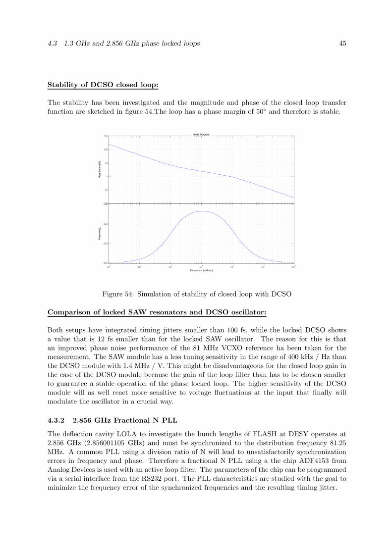
Stability of DCSO closed loop:
The stability has been investigated and the magnitude and phase of the closed loop transferfunction are sketched in figure 54.The loop has a phase margin of 50 and therefore is stable.
−100
−50
0
50
100
150
Mag
nitu
de (
dB)
103
104
105
106
107
108
109
−180
−150
−120
−90
Pha
se (
deg)
Bode Diagram
Frequency (rad/sec)
Figure 54: Simulation of stability of closed loop with DCSO
Comparison of locked SAW resonators and DCSO oscillator:
Both setups have integrated timing jitters smaller than 100 fs, while the locked DCSO showsa value that is 12 fs smaller than for the locked SAW oscillator. The reason for this is thatan improved phase noise performance of the 81 MHz VCXO reference ha been taken for themeasurement. The SAW module has a less tuning sensitivity in the range of 400 kHz / Hz thanthe DCSO module with 1.4 MHz / V. This might be disadvantageous for the closed loop gain inthe case of the DCSO module because the gain of the loop filter than has to be chosen smallerto guarantee a stable operation of the phase locked loop. The higher sensitivity of the DCSOmodule will as well react more sensitive to voltage fluctuations at the input that finally willmodulate the oscillator in a crucial way.
4.3.2 2.856 GHz Fractional N PLL
The deflection cavity LOLA to investigate the bunch lengths of FLASH at DESY operates at2.856 GHz (2.856001105 GHz) and must be synchronized to the distribution frequency 81.25MHz. A common PLL using a division ratio of N will lead to unsatisfactorily synchronizationerrors in frequency and phase. Therefore a fractional N PLL using a the chip ADF4153 fromAnalog Devices is used with an active loop filter. The parameters of the chip can be programmedvia a serial interface from the RS232 port. The PLL characteristics are studied with the goal tominimize the frequency error of the synchronized frequencies and the resulting timing jitter.

46 4 MASTER OSCILLATOR
The blockdiagram in figure 55 illustrates the entire PLL to synchronize the reference fre-quency 81.2499997 MHz and the 2.856001105 GHz oscillator.
Figure 55: LOLA PLL
The oscillator is generated by mixing the second harmonic at 200 MHz of a high stable crystaloscillator with a SAW (Surface Acoustic Wave) oscillator at 2488 MHz. The mixing productis filtered out with a bandpass filter and amplified in the end. The VCOs characteristics aresketched in figures 56, 57 and 58.
0 0.5 1 1.5 2 2.5 3 3.5 4 4.5 52.854
2.8545
2.855
2.8555
2.856
2.8565
2.857
2.8575
Tuning Voltage [V]
Out
put F
requ
ency
[GH
z]
Figure 56: Tuning slope of 2.856 GHz VCO

4.3 1.3 GHz and 2.856 GHz phase locked loops 47
0 0.5 1 1.5 2 2.5 3 3.5 4 4.5 50.2
0.4
0.6
0.8
1
1.2
1.4
1.6
Tuning Voltage [V]
Sen
sitiv
ity [M
Hz/
V]
Figure 57: Tuning sensitivity
100
101
102
103
104
105
106
107
−160
−140
−120
−100
−80
−60
−40
−20
0
20
Offsetfrequency [Hz]
Pha
se N
oise
[dB
c/H
z]
Figure 58: Free running phase noise at 2.856 GHz
Determination of output frequency: The outputput frequency of the entire PLL can becalculated like
fRF = PFD ( INT + FRAC/MOD) (27)

48 4 MASTER OSCILLATOR
where PFD is the phasedetector frequency that reads:
PFD = fREF ( ( 1 + D ) / R ) (28)
where fREF is the reference frequency and D is a input frequency doubler Bit. The outputfrequency is adjustable due to equation 27 by the variables
1. R = 0. . . 15
2. INT = 0. . . 511
3. FRAC = 0. . . 4095
4. MOD = 0. . . 4095
and a doubler Bit D to double the input frequency34. Doubler Bit D is set off and R divider isset to 4. An example for programming the registers is put in the appendix.Loop Filter: The Loopfilter used in the PLL is an active Filter using an operation amplifieras sketched in figure 59.
R1
R5R4
R2 C1
R3
C2R6
+
-
OPAMP
LT1028
Offsetvoltage
CP
0 0
Vtune
Figure 59: Loopfilter LOLA PLL
The parameters chosen for the Filter here are listed in table 6.
R1 0ΩR2 5kΩC1 10nFR3 1kΩC2 6.8nF
R435 1kΩR5 220ΩR6 1kΩ
Table 6: Loop filter parameters
34disabled here34R4, R5 and R6 for putting an offsetvoltage of 1.8 V at positve pin of operation amplifier
4.4 High Power Part for amplification of 81 MHz and 1.3 GHz signals 49
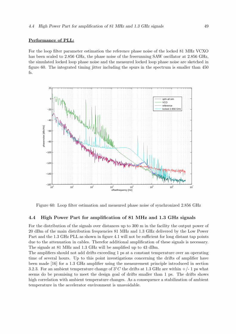
Performance of PLL:
For the loop filter parameter estimation the reference phase noise of the locked 81 MHz VCXOhas been scaled to 2.856 GHz, the phase noise of the freerunning SAW oscillator at 2.856 GHz,the simulated locked loop phase noise and the measured locked loop phase noise are sketched infigure 60. The integrated timing jitter including the spurs in the spectrum is smaller than 450fs.
100
101
102
103
104
105
106
107
−160
−140
−120
−100
−80
−60
−40
−20
0
20
offsetfrequency [Hz]
phas
enoi
se [d
Bc/
Hz]
sphi all simVCOreferencelocked 2.856 GHz
Figure 60: Loop filter estimation and measured phase noise of synchronized 2.856 GHz
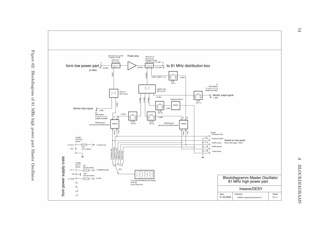
4.4 High Power Part for amplification of 81 MHz and 1.3 GHz signals
For the distribution of the signals over distances up to 300 m in the facility the output power of20 dBm of the main distribution frequencies 81 MHz and 1.3 GHz delivered by the Low PowerPart and the 1.3 GHz PLL as shown in figure 4.1 will not be sufficient for long distant tap pointsdue to the attenuation in cables. Therefor additional amplification of these signals is necessary.The signals at 81 MHz and 1.3 GHz will be amplified up to 43 dBm.The amplifiers should not add drifts exceeding 1 ps at a constant temperature over an operatingtime of several hours. Up to this point investigations concerning the drifts of amplifier havebeen made [16] for a 1.3 GHz amplifier using the measurement principle introduced in section3.2.3. For an ambient temperature change of 3C the drifts at 1.3 GHz are within +/- 1 ps whatseems do be promising to meet the design goal of drifts smaller than 1 ps. The drifts showshigh correlation with ambient temperature changes. As a consequence a stabilization of ambienttemperature in the accelerator environment is unavoidable.

50 5 SUMMARY AND CONCLUSION
5 Summary and Conclusion
The requirements of generating integrated timing jitters smaller than 100 fs could be met withthe 81 MHz and 108 MHz and with the 1.3 GHz phase locked loops using the mixing process andthe single DCSO module. The limitations for the integrated timing jitters are highly dominatedby the phase noise characeristics of the OCXO 9.027775 MHz reference module but there aredeviations from the datasheet phase noise levels and the measured ones36. In order to determinethe real phase noise at offset frequencies up to 100 Hz of the locked VCXO’s at 81 MHz, 108MHz, 1.3 GHz and the 2.856 GHz PLL the correlation factor of the measurement instrumenthas to be set to 10000 which is the maximum number N of measurement entering the formula19. The deviations of measured and simulated loop filters to minimize the integrated timingjitters especially in the case of the 1.3 GHz DCSO and the 2.856 GHz phase locked loop are aproblem that has not been solved up to now. One point to consider experimentally is to increasethe number of poles in the loop filters of the loops since the smaller proportional gain37 can notsupress the noise inside the loop bandwidth sufficently. An additional pole will also involve anew stability consideration of the loops. A smaller number of spurs in the locked loop phasenoise in the 2.856 GHz module will also improve the integrated timing jitter of this module thatwill promisingly decrease to smaller than 100 fs. The phase noise measured at 27 MHz and 13.5MHz shows also timing jitters higher than 100 fs. The theory to scale the phase noise by thedivision factor of N is not working here. The limitation can be found in the divider chips andthe additional output amplifier in the divider modules used to generate these frequencies.The investigation of harmonics shows that the modules meet the distance of harmonics to car-rier.The drift of the 1.3 GHz amplifier is in a tolerable range but the measurements have to be madefor the 81 MHz amplifier as well.The drift measurements of several RF sources has not been setup yet. The measurements in-clude two complete low power parts (LPP) and two 1.3 GHz phase locked loops driven by onereference source (figure 10). In order to localize the main causes for drifts at the outputs acomplete analytic description of the correlation of output voltages at all frequencies generatedin the two oscillator systems is necessary.New VCO’s for the 81 MHz and 108 MHz phase locked loops with superior phase noise perfor-mance have been shipped to DESY with first measurement results showing integrated timingjitters from 10 Hz to 1 MHz smaller than 55 fs. The performance of the entire distribution sys-tem includes the links of signals to remote tappoints in the facility. The sum of drifts generatedin the M.O., the power amplifiers, the locally installed PLL’s and the cables will all contributeto drifts of the reference signals at distant tappoints. The measurement of drifts in a coaxialdistribution system between distances up to 300 m at FLASH is a future research topic. Thepossibility to monitor drifts over this distance has been shown [11].
36phase noise at 9 MHz could not be measured with our instrument that works with a minimum input frequencyof 10 MHz
37due to the high tuning sensitivity of the VCO’s

Acknowledgements
I would like to thank Prof.Dr.-Ing. Schunemann for supervising this thesis and increasing myinterests for research topics at microwave frequencies.
Big thanks go to my botany companions and colleagues Jost Muller, Matthias Hoffmann,Matthias Felber, Frank Eints, Jean Randhan, Frank Ludwig and all who join us from timeto time.
I would also thank the retired PhD student Norbert Pchalek for the many interesting discussionsabout work, and many topics that go beyond that.
Harry Busse introduced me to the mystery of Tangerine Dream and he knows what I mean.Thanks go especially to all people who shared my work on the Master Oscillator like HenningWeddig, Krzysztof Czuba, Bibiane Wendland and others involved with this project.
My last but not least thanks go to Stefan Simrock who supported and still supports me forfinish my master studies and partly work on this project.

52 5 SUMMARY AND CONCLUSION
53
AB
lock
dia
gra
ms
27 MHz
Reference Oscillator81 MHz
VCXO
81 MHz
81 MHz
108 MHz
108 MHz
+20 dBm
+20 dBm
+20 dBm
+17 dBm
27 MHz+11 dBm
1
9
13.5 MHz+8 dBm
9 MHz+20 dBm
9 MHz+20 dBm
9 MHz+20 dBm
1
9
HMC 394 LP4
DDS
1 MHzTTL
50 Hz
Blockdiagramm Master Oszillator"low power" part
Inwave/DESY
19.08.2005MO_low_power_Block_first assembly 1 1
exte
rnal fr
eq. contr
ol
voltage
Amp
G = 16 dB
G = 16 dB
Amp
Pout = 26 dBm
108 MHz
VCXO
1
12
Amp
G = 16 dB
9 MHzTTL
-20 dB
+26 d
Bm
+26 d
Bm
-20 dB
0 dBm
0 dBm
-3 dB
-3 dB
-3 dB
-3 dB
-3 dB
-3 dB
3
1
HMC 394 LP4
27 MHz+11 dBm
13.5 MHz+8 dBm
2
1
108 MHz+20 dBm
to cable 13 (Experimental Hall)
to cable 12 (RF Gun Laser hut 1)
108 MHz+17 dBm
to cable 33 (RF Gun Laser hut 2)
108 MHz+20 dBm
spare
Power Divider in Distribution box
to Cable 8 ( EOS hut)
to Cable 15 (Experimental Hall)
to cable 10 (old TTF Control room)
to Timing System
to Timing System
to Timing System
to cable xx (RF Gun Laser hut 1)
to cable yy (RF Gun Laser hut 2)
to cable aa (RF Gun Laser hut 1)
to cable bb (RF Gun Laser hut 2)
to 81 MHz power Amplifier Box
spare
to 81 MHz power Amplifier (for 1517 MHz Multiplier)
+20 dBm
+20 dBm
+17 dBm
+17 dBm
+10 d
Bm
+10 d
Bm
VCXOPA 81
PLL 81 MHz
-3 dB
81 MHz / +20 dBm
VCXOPA108
PLL 108 MHz
PA 9 MHz
first assembly
9 MHz+20 dBm
spare
HMC 394 LP4
9 M
Hz E
CL p
uls
es
27 M
Hz E
CL p
uls
es
1 MHz
+8 dBm
1 MHz
+8 dBm
9
1
HMC 394 LP4
+9 dBm
+9 dBm
PD
J1
J2
J3
J4
J7
Sheet
of
Title
created
file nameDate
J8
J9
J10
J11
J13
J14
J16
PD
J17
J15
J18
J5
J6
J19
J20
10 dB
10 dB
J22
J21
J23
J24
J25
J26
J27
J28
J29
J30 J31
J32
J33
J34
J12
J35
J36
J37
J38
J39
J40
J41
J42
Figu
re61:
Blo
ckdiagram
lowpow
erpart
Master
Oscillator
54A
BLO
CK
DIA
GR
AM
S
81 MHz
main line loss = 0,3 dB
+20 dBm
Blockdiagramm Master Oszillator81 MHz high power part
Inwave/DESY
21.03.2006 1300MHz_highpoweramp_Block.sch
Power amp
+40 dBm
0 d
Bm
+20 d
Bm
+14 d
Bm
main line loss = 0,3 dB
+39.7 dBm
-6 dBm
0 dBm (VSWR = 1.2)
+14 d
Bm
-6 dBm
Tra
nsd
uce
r G
ain
Tra
nsducer
Phase
VS
WR
(lo
g v
alu
e)
VS
WR
Phase
AD8302 board:
Transducer Gain
Transducer phase
VSWR (value)
VSWR (phase)
Socket on rear panel(Doocs data logger + Alarm)
+12 V
Gnd
+5 V DVM
to AD8302 boards
to DVM
to power amp+12 V/5 A
Gnd
from
pow
er
supply
cra
tecoupling = 20 dB
coupling = 20 dB
to 81 MHz distribution boxform low power part
Monitor Input signal
-3 d
Bm
-3 dBm
Monitor output signal
Output power
Ou
tpu
t p
ow
er
-12 dBm
-6 dBm
1 1
+14 d
Bm
+14 dBm
with internal 20 dB Attenuators
AD8302 board:
with internal 20 dB Attenuators
+4 dBmAmplitude Detector
J1 J2
ZFSC-2-1
Mini Circuits
3 1/2 Digit DVM Module (LED Display)
DPM 340
Lascar Electronics
ZFDC-20-1H
Mini Circuits
In1
In2
Ga
in
Phase
AD8302
In1
In2
Ga
in
Phase
AD8302
20 dB
VAT-20
20 dB
VAT-20
Date Sheet
of
Filename
SW1
FS1
6.3 A medium
J3
SMA Adapter
37_50_0-1/111_N
HUBER+SUHNER
ZB4PD1-500
Mini Circuits
AD8361
20 dB
VAT-20
ZFDC-20-3
Mini Circuits
6 dB
VAT-6
10 dB
VAT-10
J4
SMA Adapter
37_50_0-1/111_N
HUBER+SUHNER
1
2
3
4
5
6
7
8
9
CONN1
1
2
3
CONN2
NC3FXCC
Neutrik
1
2
3
4
5
6
7
CONN3
NC7FX
NeutrikFS2
200 mA medium
FS3
200 mA medium
Figu
re62:
Blo
ckdiagram
of81
MH
zhigh
pow
erpart
Master
Oscillator

55
1300 MHz
main line loss = 0,3 dB
+20 dBm
Blockdiagramm Master Oszillator"1.3 GHz high power part"
Inwave/DESY
15.03.2006 1300MHz_highpoweramp_Block.sch
1
Power amp
+44 dBm
DVM module on front panel with five position switchto monitor amplitude and phase detector voltagesLED´s for monitoring supply voltagesSupply voltage for Phase and amplitude detector + 5 V
-10 d
Bm
+14 d
Bm
+8 d
Bm
main line loss = 0,3 dB
+43.7 dBm
-12 dBm
-6 dBm (VSWR = 1.2)
+8 d
Bm
-12 dBm
Tra
nsd
uce
r G
ain
Tra
nsducer
Phase
VS
WR
(lo
g v
alu
e)
VS
WR
Phase
AD8302 board: with internal 20 dB Attenuators
AD8302 board: with internal 20 dB Attenuators
Transducer Gain
Transducer phase
VSWR (value)
VSWR (phase)
to 9 pin Sub-min D socket on rear panel
(Doocs data logger + Alarm)
+12 V
Gnd
+Vs DVM
to AD8302 boards
to DVM
to power amp+12 V/5 A
Gnd
from
pow
er
supply
cra
tecoupling = 30 dBcoupling = 30 dB
to 1.3 GHz distribution boxfrom 1.3 GHz PLL
Monitor Input signal
-13 d
Bm
-13 dBm
Monitor output signal
Output power
Ou
tpu
t p
ow
er
-12 dBm
-12 dBm
AM38-1.3S-23-43
Microwave Amplifiers Ltd.
J1 J2
ZN2PD-20
Powersplitter
3 1/2 Digit DVM Module (LED Display)
3194-30
ARRA
3194-30
ARRA
In1
In2
Ga
in
Phase
AD8302
In1
In2
Ga
in
Phase
AD8302
20 dB 20 dB
6 dB
Date Sheet
of
Filename
50
SW1
J4
J5
J6
J7
J8
J9
J10
J11
J12 FS1
6.3 A medium
J13
ZB4PD1-2000
Mini CircuitsJ14
AD8361 Amplitude Detector
J15
10 dB
10 dB
Figu
re63:
Blo
ckdiagram
of1300
MH
zhigh
pow
erpart
Master
Oscillator

56 B PROGRAMMING THE ADF4153
B Programming the ADF4153
For synchronizing the deflection cavity with the help of a fractional N divider synthesizer chipthe registers in the chip have been programmed as follows.Programming the Registers:
4 registers should be programmed [7]Example: Bit pattern for synchronizing LOLA loading numbers:
reg0=reg0 (for decimal 0)reg1=reg327681 (for bitpattern:1010000000000000001)reg2=reg578 (for bitpattern:1001000010) or reg2=reg514 for inversed polarity of phasedetectorwith bitpattern : 1000000010reg3=reg967 (for bitpattern:1111000111)and the values for INT, FRAC and MOD should be entered like frac0. . . frac4095 [+ Enter].Here:frac612mod1015int140

REFERENCES 57
References
[1] vuv-fel.desy.de, 2006.
[2] Application Note Aeroflex/Comstron. Phase noise theory and measurement. Internet,www.aeroflex.com.
[3] Wenzel Associates. Datasheet of 9.0277775 MHz - SC Streamline Crystal oscillator.www.wenzel.com.
[4] B.Lorbeer. Phase Noise Measurements of the new Master Oscillator for TTF2. DESY-THESIS-2004-023, July 2004.
[5] Heinz-J B.Schiek. Rauschen in Hochfrequenzschaltungen.
[6] ANALOG DEVICES. Datasheet of AD8302. www.analog.com.
[7] ANALOG DEVICES. Datasheet of ADF4153. www.analog.com.
[8] Frank Ludwig et. al. Phase stability of the next generation RF field control for VUV-and
X-Ray FEL. EPAC, 2006.
[9] Hittite. Datasheet of HMC 394. www.hittite.com.
[10] Hittite. Datasheet of HMC 440. www.hittite.com.
[11] K.Czuba. First generation of optical fiber phase reference distribution system for TESLA.TESLA REPORT 2005-08, 28.02.2005.
[12] M.Felber. A Feedback System based on Optical Fiber for compensating RF-Phase Drifts.Diplomarbeit in Physikalische Technik an der Fachhochschule Wedel, February 2006.
[13] Bernd Neubig. Quarzkockbuch. www.axtal.de.
[14] Application Note/Hewlett Packard. Phase noise characterization of microwave oscillators.Product Note: 11729C-2. Frequency discriminator method.
[15] Werner Schnorrenberg. Rauschmessung mit dem spektrumanalysator. Mikrowellen und HF
Magazin, Vol.16(No.2), 1990.
[16] Karol Suchecki. Phase drift measurements of power amplifier. Laboratory report LLRF(internal logbook DESY), 2006.
[17] Linear Technology. Datasheet from OP LT1028. www.linear.com.
[18] Application Note 5989-1617EN Agilent Techologies. Advanced phase noise and transientmeasurement techniques. Internet, www.agilent.com.
[19] Application Note 5989-1617EN Agilent Techologies. Model pll dynamics and phase-noiseperformance. Microwaves and RF, February 2000.
[20] Thumm/Wiesbeck/Kern. Hochfrequenzmesstechnik, Verfahren und Messysteme.B.G.Teubner Stuttgart Leipzig, 1998.
[21] Henning Weddig. Requirements for the new m.o. for ttf2. DESY Document.

Confirmation
I confirm that i have written the thesis myself and only the references mentioned have beenused.