sputterdepositionofnanocrystalline -sic ... · and in various rhombohedral or hexagonal high...
TRANSCRIPT

RESEARCHARTICLE
Copyright © 2010 American Scientific PublishersAll rights reservedPrinted in the United States of America
Journal ofNanoscience and Nanotechnology
Vol. 10, 1–9, 2010
Sputter Deposition of Nanocrystalline �-SiCFilms and Molecular Dynamics
Simulations of the Sputter Process
Carlos Ziebert1�∗, Jian Ye1, Sven Ulrich1, Alen-Pilip Prskalo2, and Siegfried Schmauder21Institute for Materials Research I, Forschungszentrum Karlsruhe, Hermann-von-Helmholtz-Platz 1, 76344
Eggenstein-Leopoldshafen, Germany2Institute for Materials Testing, Materials Science and Strength of Materials (IMWF), University of Stuttgart,
Pfaffenwaldring 32, 70569 Stuttgart, Germany
Thin nanocrystalline films of silicon carbide (SiC) have been deposited on Si substrates by rfmagnetron sputtering in pure Ar atmosphere. Simultaneously classical molecular dynamics (MD)simulations of sputtering of �-SiC by Ar atoms were performed using IMD and Materials Explorersoftware with a combination of the Tersoff and the Ziegler-Biersack-Littmark (ZBL) potential in orderto get more insight into the sputter process. In experiments the bias voltage (0 to −40 V) has beenvaried at constant substrate temperature of 900 �C to investigate the influence on the composition,the constitution and the mechanical properties of crystalline �-SiC films. At second the substratetemperature has been varied between 900 �C and 100 �C to find the minimum substrate temper-ature that is needed to get nanocrystalline �-SiC under the applied sputter conditions (ceramicSiC target, 300 W rf power, 18 cm target-substrate distance, 50 sccm Ar gas flow, 0.26 Pa totalgas pressure). The films have been characterized by electron probe micro-analysis (EPMA), X-raydiffraction (XRD), Raman spectroscopy and atomic force microscopy (AFM). Hardness and residualstress have been investigated by nanoindentation and wafer bending. In the MD simulations thesputter yield was determined as a function of the energy of the incident Ar atoms (in the interestingrange for sputter deposition, i.e., 50–1000 eV). To our knowledge this is the first time that the sputteryield of a SiC target was determined as a function of the energy of the incident Ar atoms in the lowenergy range by using MD simulations and compared with experimental results.
Keywords: Magnetron Sputtering, Silicon Carbide, Nanoindentation, Molecular DynamicsSimulation, Sputter Yield.
1. INTRODUCTION
Due to their mainly covalent bonding silicon carbide (SiC)thin films are of great scientific and technological inter-est because of their excellent properties such as goodcorrosion and wear resistance, high hardness, chemicalinertness, high thermal stability and good electric con-ductivity. These material characteristics make it attractivefor semiconductor applications (high temperature electron-ics, high frequency devices, optoelectronic application),for protective coatings against corrosion of steel, X-raymask materials and protection of thermonuclear reactorwalls.1 SiC can appear in different crystal structures: ina metastable, cubic low temperature modification (�-SiC)
∗Author to whom correspondence should be addressed.
and in various rhombohedral or hexagonal high tempera-ture modifications (�-SiC), which form from �-SiC above1000 �C.2 The polytypes of �-SiC differ in the orien-tation and the stacking sequence of subsequent tetrahe-dron layers. The most common types are 4-H-, 6-H- und15-R-�-SiC. A great advantage of SiC is that the mechan-ical properties of the �- and the �-phase do not differas much as in the case of graphite/diamond or cubic andhexagonal boron nitride. Moreover under high compressivestress �-SiC can become superhard.
Various techniques have been applied to deposit crys-talline SiC films such as: CVD,3–8 reactive and non-reactive magnetron sputtering,1�9–14 molecular ion beamdeposition,15�16 pulsed laser deposition17�18 and ion implan-tation.19 For industrial applications crystalline SiC coatingsare mainly deposited by chemical vapour deposition (CVD)
J. Nanosci. Nanotechnol. 2010, Vol. 10, No. xx 1533-4880/2010/10/001/009 doi:10.1166/jnn.2010.1842 1
RESEARCHARTICLE
Sputter Deposition of Nanocrystalline �-SiC Films and MD Simulations of the Sputter Process Ziebert et al.
at typical deposition temperatures of more than 1000 �C.These CVD methods usually use hydrogen-containing pro-cess gases such as methane (CH4�, silane (SiH4� or HMDS(Si(CH3�6�, which can lead to a high content of bondedhydrogen (10–30 at.%) in the growing films, and thus toSiCx:H coatings. To deposit hydrogen-free SiC coatings,the PVD methods are more appropriate, because they canalso work with pure Ar process gas. Generally, at lowdeposition temperatures (T < 700 �C) and medium or highgrowth rates (R ≥ 5 nm/min) sputtered SiC coatings areamorphous. However, Ulrich et al.10 succeeded in deposit-ing hard nanocrystalline �-SiC coatings with a crystallitesize of 20 nm by r.f. magnetron sputtering of a SiC targetin pure argon plasma at a low substrate temperature of only420 �C. They showed that intense argon ion bombardment(high ion flux and low ion energies) during film growth andlow growth rates (R < 5 nm/min) are required.
In the case of large systems (number of atoms > 1000)the classical molecular dynamics (MD) method is wellsuited for the simulation of structural and mechanicalproperties of materials at the atomic scale. In this methodthe atoms of a solid are regarded as point particles, whichinteract by classical potential functions. The Newton equa-tions of motion are numerically integrated, with the pos-sibility to take into account certain conditions, such asexternal forces or deformations and to use various thermo-dynamic ensembles, such as the canonical NVT ensemble(i.e., a system with a constant volume in contact with aheat bath of constant temperature). From the configura-tions, which are calculated in the MD simulation, energies,stresses, distortions and elastic constants can be locallydetermined. For the simulation of covalent solids, as in thecase of SiC/Si3N4 multilayer films, multi-body potentialsare necessary, because directed bonds are occurring. Thesepotentials can be subdivided into two main categories, onthe one hand those potentials, which can be split into two-and three-body parts and on the other hand, the bond-orderpotentials. The most popular potential of the first class isthe Stillinger-Weber potential,20 for the second class themost popular representative is the Tersoff potential.21�22
Sputtering is the removal of target atoms by ion bom-bardment. The quantitative value for this removal is thesputtering yield, defined as the number of removed atomsor molecules per incident ion. To simulate the sputter pro-cess in the thin film deposition the ZBL (Ziegler-Biersack-Littmark) potential was developed23 and later combinedwith the multi-body potentials mentioned above. MD sim-ulations of sputter processes make especially sense forlow process energies below 1 keV. At higher energies thesingle collision cascades are spatially separated and thebinary collision approximation in the form of Monte Carlo(MC) simulations can be used,24 which is implementedin such widespread codes as TRIM25 and TRIDYN.26 In1988 Harrison made pioneering work when he investi-gated collision cascades by MD simulations using the
simple pair potentials for metals and noble gases avail-able at that time. He showed important principles, suchas e.g., channelling and blocking mechanisms of surfaceatoms, which are responsible for the emission pattern ofthe sputtered particles.27 For the bombardment of cova-lent materials similar sputter mechanisms were found, butthe open lattice structures allowed stronger contributionsfrom the second and third atomic layers as in the case ofmetals.28 In 2002 Ecke et al. compared the experimentalsputter yields of SiC for bombardment of Ar ions in theenergy range between 0.5 and 5 keV under 60� sputter-ing with MC simulations using the programs TRIM andT-DYN. They reported that the differences between theresults of the simulation programs are sometimes greaterthan their difference from the experimentally measuredsputter yields.29 Later Kosiba performed TRIDYN simula-tions and compared them to his experimental results fromAuger spectroscopy.30 In 2004 Shapiro et al. investigatedthe influence of the interatomic potential on the resultsof MD simulations of the sputter process and showedthat most sputter parameters are relatively independent onthe choice of the potential.31
Our overall research goal is to use molecular dynamicssimulations in combination with experimental validationfor the development of improved SiC and Si3N4 single-and bilayer coatings, and multilayer SiC/Si3N4 nanolami-nates, which are deposited by magnetron sputtering ontosilicon and/or steel. As the first experimental step thinSiC films have been deposited by rf magnetron sputter-ing with systematic variation of the substrate temperatureand the bias voltage and the influence of these deposi-tion parameters on the constitution, the microstructure andthe mechanical properties were investigated to find out,whether it is possible to deposit nanocrystalline b-SiCfilms with the chosen sputter set-up. As the first MD sim-ulation step the sputtering of a �-SiC-target at 700 K byargon was simulated using the Tersoff potential for theSi–C interaction and tabulated ZBL pair potential for theinteraction with argon. Of course it would have been niceto compare the experimental results of a deposition processdirectly with MD simulations. However, for the MD sim-ulations it is necessary at first to get more insight into thesputtering process, because this gives the necessary inputparameters for the MD simulation of the SiC depositionprocess. To our knowledge this is the first time that thesputter yield of a SiC target was determined as a functionof the energy of the incident Ar atoms in the low energyrange by using MD simulations and compared with exper-imental results.
2. EXPERIMENTAL DETAILS
2.1. Deposition
The SiC-films were produced in a PVD-CVD hybridcoating machine consisting of an electron cyclotron
2 J. Nanosci. Nanotechnol. 10, 1–9, 2010

RESEARCHARTICLE
Ziebert et al. Sputter Deposition of Nanocrystalline �-SiC Films and MD Simulations of the Sputter Process
resonance (ECR) microwave plasma beam source, anECR-microwave ion gun, three magnetron sputter sources(target-substrate distance 18 cm) and a heatable substrateholder where a variable substrate bias voltage can beapplied. The films were prepared in unbalanced rf mag-netron sputtering mode at a power of 300 W at substratetemperatures between 100 and 900 �C and bias voltagesup to −40 V without making use of the ECR components.The target was a hot pressed SiC target (diameter =75 mm, thickness = 6 mm, purity = 99.95%). Double-side polished, (100)-oriented silicon wafers were used asthe substrates. Prior to the film deposition, the substrateswere ultrasonically cleaned in isopropanol, and addition-ally cleaned by argon ion beam etching for 10 min eachat deposition temperature with a bias voltage of −400 V.The base pressure before deposition was lower than 3×10⁻⁴ Pa and a working pressure of 0.26 Pa was adjustedby 50 sccm Ar gas flow.
2.2. Characterization
The coating thickness has been measured by a surfaceprofilometer (type Tencor P-10). Chemical compositionwas investigated by using EPMA (type Cameca Came-bax Microbeam). The surface topography was studied bymeans of AFM (Digital Instruments Inc., Dimension 3100)with a Si tip (Nanosensors LFM-20; tip radius < 10 nm)in contact mode. The crystal structure was investigated byXRD (Seifert Company, PAD II) with Cu K� radiation.The measured diffractograms have been fitted by pseudo-Voigt functions using the Rietveld program LS1 developedby Lutterotti et al.,32 which allows the determinationof the crystallite sizes and the lattice constants.33 Thebonding characteristics has been investigated by Ramanspectroscopy (type Renishaw micro-Raman spectroscopysystem 1000). As mechanical properties, nanohardness H ,reduced Young’s modulus E∗ (CSIRO, UMIS2000) andresidual stress �r (wafer bending method, type TencorP-10) were measured. Nanohardness and reduced Young’smodulus were determined from load versus penetrationdepth curves using the Oliver-Pharr method34 and theASMEC Indentanalyser software at a maximum appliedload of 10 mN to reduce both the influence of the surfaceroughness and of the substrate.
3. COMPUTATIONAL METHODS
By classical molecular dynamics the sputter process forthe �-SiC target material by Ar atoms was simulated to getadditional information on the expected sputter yields. Forthe modelling of the short-range interaction, the tabulatedZBL potential was used and for modelling the Si–C inter-action the Tersoff classical potential was chosen, which hasbeen used before successfully in several SiC studies.35–37
Especially when the overall computational workload is
massive, using the Tersoff potential is better than tight-binding or ab initio potentials. For the MD simulationsboth the commercial software package Materials Explorer4.0 (ME) (Fujitsu Ltd.) and the MD program package IMD(ITAP Molecular Dynamics),38�39 which was developed atthe university of Stuttgart and is suited for many platformsfrom a single PC to a massively parallel supercomputer,were used. A comparison of these two different softwarepackages seems interesting, because they have differentadvantages and disadvantages which have to be comparedand if possible their advantages combined to get betterMD simulation results. E.g., ME possesses a better graph-ical interface and is easier to use, but the maximum blocksize is limited. In both cases periodic boundary conditionswere applied at the lateral (x� y) boundaries to mimic asemi-infinite surface and remove edge-effects and the sim-ulations cells had an open top layer in the +z direction.In the ME simulations, i.e., those performed with the MEsoftware, the C-terminated �-SiC single crystal target hasa size of 8× 8× 12 units cells consisting of 6144 atomswith the density of about 3.3 g/cm3. In the IMD simu-lations the dimensions are 10 × 10 × 20 unit cells, i.e.,16000 atoms. The chosen unit cell size for the ME isthe maximum size that can be simulated by the MaterialsExplorer Software, which is running on a single Windowsworkstation. Because the IMD software, which is runningin parallel on a high performance cluster, allows a largerunit cell size, this larger size was chosen for the IMD sim-ulations. The chosen cell height made sure that the incidentAr ions transfer all their energy to the SiC target and thechosen cell width ensures that the Ar ions do not hit theboundaries.
The same number of Si and C atoms was initially placedon the diamond lattice and an equilibration of the targetat 673 K for 1 ps using the NPT-ensemble with externalpressure control by the Parinello-Rahman method40 andtemperature control by the Nose-Hoover thermostat41�42
was performed. The interaction potentials were used tocalculate forces, and the Newtonian equations of motionswere solved using the Gear method employing a five-valuepredictor-corrector scheme43 with the time-step 1 fs. 50thermally equivalent samples were prepared for the subse-quent simulation of the sputter process to achieve statistics.After the equilibration the atoms in the two bottom lay-ers were fixed to prevent unphysical centre-of-mass driftof the lattice caused by the momentum transfer from thebombarding ion.44
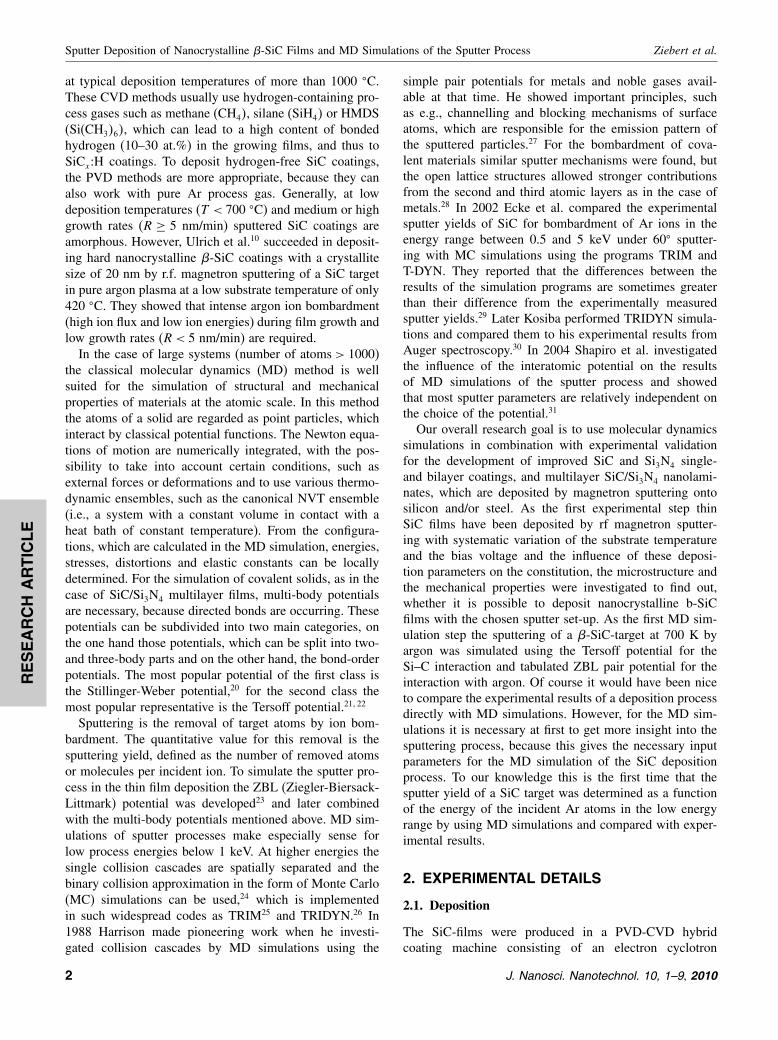
To simulate the sputter process two different procedureswere applied using the microcanonical NVE ensemble.In the ME simulations an area of 1.2 nm× 1�2 nm waschosen on the SiC (001) surface. Starting at a height of2 nm above the surface one randomly oriented (on thex–y plane) Ar ion at an incident angle of 0�, measuredfrom the macroscopic surface normal, with a fixed energywas allowed to impact this surface area. For the IMD simu-lations 9 coordinates were defined according to the crystal
J. Nanosci. Nanotechnol. 10, 1–9, 2010 3
RESEARCHARTICLE
Sputter Deposition of Nanocrystalline �-SiC Films and MD Simulations of the Sputter Process Ziebert et al.
Fig. 1. Definition of the 9 coordinates for a C-terminated SiC-surface.
symmetry of the zincblende structure as shown schemati-cally in Figure 1, and for every coordinate the MD sim-ulations were performed for one Ar ion that impacts theSiC (001) surface at this coordinate at 0� and fixed energy.Coordinate Nr. 1 is an atom of the topmost C layer, coor-dinate Nr. 2 is an atom of the layer below, which is thefirst Si layer, Nr. 3 is in the third layer, i.e., the secondC layer and Nr. 4 is in the second Si layer. The other coor-dinates are selected in the centres between the layers (Nr.5–8) and in the free space (Nr. 9). Thus there is no cova-lent Si–C bonding for Nr. 5 in contrast to Nr. 6, 7 and 8,which are situated below by 1/4 of the lattice constant.
The experimental sputtering yield is an average ofnumerous sputtering events. In simulations, especially athigher energies, the yield can vary from zero to severalthousand atoms per ion between individual events. A sin-gle large yield event can increase the average yield signifi-cantly and the results are very sensitive to whether a singleevent is included in an average or not. To compare simu-lated results to experimental values it is necessary to runenough simulations with different random initial values.45
Therefore in both procedures 50 simulations have beenperformed for every ion energy in order to stabilize thecalculated average sputter yield. A simulation time of 2 pswas chosen to ensure that the individual atoms oscillatearound a momentarily stable average distance from theirequilibrium bulk positions after the impact. The sputteryield was calculated from the final states of the simula-tions as a function of the incident energy of the argonions, which was varied between 50 eV and 1 keV, whichis the interesting range for sputter deposition. An atom oran atom cluster is considered sputtered, if it is more than0.6 nm away from the surface, which is twice the cut-offdistance of the potentials. Furthermore, the trajectories of
the Ar atoms and the ranges of Ar ions and sputtered Siand C atoms were determined from the simulation data.
4. RESULTS AND DISCUSSION
4.1. Experimental Results
4.1.1. Constitution
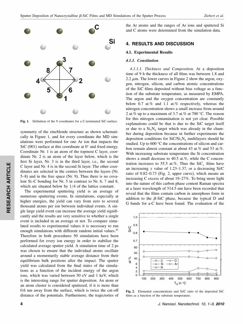
4.1.1.1. Thickness and Composition. At a depositiontime of 9 h the thickness of all films was between 1.8 and2.2 �m. The lower curves in Figure 2 show the argon, oxy-gen, nitrogen, silicon, and carbon atomic concentrationsof the SiC films deposited without bias voltage as a func-tion of the substrate temperature, as measured by EMPA.The argon and the oxygen concentration are constantlybelow 0.7 at.% and 1.1 at.% respectively, whereas thenitrogen concentration shows a small increase from around2 at.% up to a maximum of 3.7 at.% at 700 �C. The reasonfor this nitrogen contamination is not yet clear. Possibleexplanations could be that is due to the SiC target itselfor due to a Si3N4 target which was already in the cham-ber during deposition because in further experiments thedeposition conditions for SiC/Si3N4 multilayers should bestudied. Up to 600 �C the concentrations of silicon and car-bon remain almost constant at about 43 at.% and 53 at.%.With increasing substrate temperature the Si concentrationshows a small decrease to 40.5 at.%, while the C concen-tration increases to 55.5 at.%. Thus the SiCx films havean increasing x value of 1.23–1.37, or a decreasing Si/Cratio of 0.82–0.73 (Fig. 2, upper curve), which means anincreasing C excess of about 19–27%. To bring more lightinto the nature of this carbon phase content Raman spectraat a laser wavelength of 514.5 nm have been recorded thatreveal that the films contain carbon in amorphous form inaddition to the �-SiC phase, because the typical D andG bands for a-C have been found. The evaluation of the
100 200 300 400 500 600 700 800 9000246
40
50
60
0.7
0.8
0.9
1.0
C OSi ArN
at %
TS in °C
Si/C
Fig. 2. Elemental concentrations and Si/C ratio of the deposited SiCfilms as a function of the substrate temperature.
4 J. Nanosci. Nanotechnol. 10, 1–9, 2010
RESEARCHARTICLE
Ziebert et al. Sputter Deposition of Nanocrystalline �-SiC Films and MD Simulations of the Sputter Process
Raman spectra showed that with increasing substrate tem-perature the D and G bands show an increasing separation,which indicates increasing graphitisation. This graphitisa-tion is even more pronounced for the film with highersubstrate bias. Concerning the dependence of the chemicalcomposition on the bias voltage at constant substrate tem-perature of 900 �C no significant dependence was found.In contrast to Lattemann et al.14 no decreasing Si concen-tration due to increasing resputtering of Si was observedwith increasing bias voltage.4.1.1.2. Crystal Structure. Figure 3 shows the evolu-
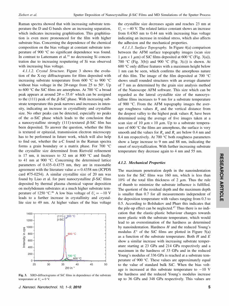
tion of the X-ray diffractograms for films deposited withincreasing substrate temperature from 600 �C to 900 �Cwithout bias voltage in the 2�-range from 25 to 50�. Upto 600 �C the SiC films are amorphous. At 700 �C a broadpeak appears at around 2� = 35�6� which can be assignedto the (111) peak of the �-SiC phase. With increasing sub-strate temperature this peak narrows and increases in inten-sity, indicating an increase in crystallinity and crystallitesize. No other peaks can be detected, especially no peaksof the �-SiC phase which leads to the conclusion thata nanocrystalline strongly (111)-textured �-SiC film hasbeen deposited. To answer the question, whether the filmis textured or epitaxial, transmission electron microscopyhas to be performed in future work, which will also helpto find out, whether the a-C found in the Raman spectraforms a grain boundary or a matrix phase. For 700 �Cthe crystallite size determined from Rietveld refinementis 17 nm, it increases to 32 nm at 800 �C and finallyto 41 nm at 900 �C. Concerning the determined latticeparameters of 0.435–0.4375 nm, they are in reasonableagreement with the literature value a= 0�4358 nm (JCPDScard #75-0254). A similar crystallite size of 20 nm wasfound by Liao et al. for pure nanocrystalline �-SiC filmsdeposited by thermal plasma chemical vapour depositionon molybdenum substrates at a much higher substrate tem-perature of 1250 �C.46 A low bias voltage of Us =−10 Vleads to a further increase in crystallinity and crystal-lite size to 49 nm. At higher values of the bias voltage
25 30 35 40 45 500
200
400
600
800
1000
1200
1400
700 °C
800 °C
900 °C
600 °C
Inte
nsity
in c
ps
2Θ in °
(111)β-SiC
Fig. 3. XRD-diffractograms of SiC films in dependence of the substratetemperature at Us = 0 V.
the crystallite size decreases again and reaches 23 nm atUs =−40 V. The related lattice constant shows an increasefrom 0.4365 nm to 0.44 nm with increasing bias voltageindicating an increase in residual stress, which also affectsthe adhesion and the mechanical properties.4.1.1.3. Surface Topography. In Figure 4(a) comparison
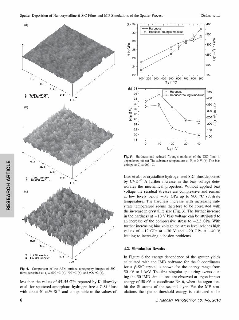
between the AFM surface topography images (scan size1 �m×1 �m) of SiC films deposited at 600 �C (Fig. 3(a)),700 �C (Fig. 3(b)) and 900 �C (Fig. 3(c)) is shown. At600 �C only diffuse features with a maximum height below1 nm can be seen, which confirms the amorphous natureof this film. The image of the film deposited at 700 �Cshows small rounded structures with an average diameterof 7 nm as determined by the grain size analysis methodof the Nanoscope AFM software. This size which can beregarded as the lateral crystallite size of the nanocrys-talline films increases to 9 nm for a substrate temperatureof 900 �C. From the AFM topography images the aver-age roughness values Ra and the vertical distance fromthe deepest valley to the highest peak values Rt have beendetermined using the average of five images taken at ascan size of 10 �m× 10 �m. Up to a substrate tempera-ture of 600 �C the films are amorphous, the surface is verysmooth and the values for Ra and Rt are below 0.4 nm and8.4 nm respectively. At 700 �C both roughness parametersshow a large increase to 9 nm and 88 nm, indicating theonset of recrystallization. With further increasing substratetemperature they decrease again to 4 nm and 55 nm.
4.1.2. Mechanical Properties
The maximum penetration depth in the nanoindentationtests for the SiC films was 160 nm, which is less than10% of the total film thickness of 2 �m. Thus the ruleof thumb to minimize the substrate influence is fulfilled.The quotient of the residual depth and the maximum depthis smaller than 0.7 for all measurements independent ofthe deposition temperature with values ranging from 0.3 to0.5. According to Bolshakov and Pharr this indicates thatthe pile-up effect can be neglected.47 Thus there is no indi-cation that the elastic-plastic behaviour changes towardsmore plastic with the substrate temperature, which wouldlead to an overestimation of the hardness as determinedby nanoindentation. Hardness H and the reduced Young’smodulus E∗ of the SiC films are plotted in Figure 5(a)as a function of the substrate temperature. Both H and Eshow a similar increase with increasing substrate temper-ature starting at 23 GPa and 214 GPa respectively and amaximum in the hardness of 33 GPa and in the reducedYoung’s modulus of 336 GPa is reached at a substrate tem-perature of 900 �C. These values are approximately equalto the value of standard bulk SiC. When the bias volt-age is increased at this substrate temperature to −10 Vthe hardness and the reduced Young’s modulus increaseup to 36 GPa and 348 GPa respectively. This values are
J. Nanosci. Nanotechnol. 10, 1–9, 2010 5
RESEARCHARTICLE
Sputter Deposition of Nanocrystalline �-SiC Films and MD Simulations of the Sputter Process Ziebert et al.
(a)
(b)
(c)
Fig. 4. Comparison of the AFM surface topography images of SiC-films deposited at Ts = 600 �C (a), 700 �C (b), and 900 �C (c).
less than the values of 45–55 GPa reported by Kulikovskyet al. for sputtered amorphous hydrogen-free a-C:Si filmswith about 40 at.% Si 48 and comparable to the values of
100 200 300 400 500 600 700 800 90022
24
26
28
30
32
34
HardnessReduced Young′s modulus
TS in °C
(a)
(b)
H in
GP
a
150
200
250
300
350
400
E/(
1–ν2 )
in G
Pa
0 –10 –20 –30 –4018
20
22
24
26
28
30
32
34
36
38HardnessReduced Young′s modulus
US in V
H in
GP
a
100
150
200
250
300
350
400
450
E/(
1–ν2 )
in G
Pa
Fig. 5. Hardness and reduced Young’s modulus of the SiC films independence of: (a) The substrate temperature at Us = 0 V. (b) The biasvoltage at Ts = 900 �C.
Liao et al. for crystalline hydrogenated SiC films depositedby CVD.46 A further increase in the bias voltage dete-riorates the mechanical properties. Without applied biasvoltage the residual stresses are compressive and remainat low levels below −0.7 GPa up to 900 �C substratetemperature. The hardness increase with increasing sub-strate temperature seems therefore to be correlated withthe increase in crystallite size (Fig. 3). The further increasein the hardness at −10 V bias voltage can be attributed toan increase of the compressive stress to −2.2 GPa. Withfurther increasing bias voltage the stress level reaches highvalues of −12 GPa at −30 V and −20 GPa at −40 Vleading to increasing adhesion problems.
4.2. Simulation Results
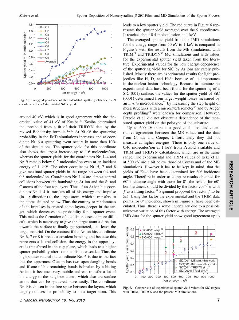
In Figure 6 the energy dependence of the sputter yieldscalculated with the IMD software for the 9 coordinatesfor a �-SiC crystal is shown for the energy range from50 eV to 1 keV. The first singular sputtering events dur-ing the 50 IMD simulations are observed at argon impactenergy of 50 eV at coordinate Nr. 6, when the argon ionshit the Si atoms of the second layer. For the ME sim-ulations the sputter threshold energy is estimated to be
6 J. Nanosci. Nanotechnol. 10, 1–9, 2010
RESEARCHARTICLE
Ziebert et al. Sputter Deposition of Nanocrystalline �-SiC Films and MD Simulations of the Sputter Process
0 200 400 600 800 1000
0.0
0.2
0.4
0.6
0.8
1.0
1.2
1.4
1.6
1.8S
putte
r yi
eld
Y i
n m
olec
ules
/ion
Ion energy in eV
C1C2C3C4C5C6C7C8C9Average
Fig. 6. Energy dependence of the calculated sputter yields for the 9coordinates for a C-terminated SiC crystal.
around 40 eV, which is in good agreement with the the-oretical value of 41 eV of Kosiba.30 Kosiba determinedthe threshold from a fit of their TRIDYN data by therevised Bohdansky formula.49�50 At 90 eV the sputteringprobability in the IMD simulations increases and at coor-dinate Nr. 6 a sputtering event occurs in more then 10%of the simulations. The sputter yield for this coordinatealso shows the largest increase up to 1.6 molecules/ion,whereas the sputter yields for the coordinates Nr. 1–4 andNr. 9 remain below 0.2 molecules/ion even at an incidentenergy of 1 keV. The other coordinates Nr. 5, 7 and 8give maximal sputter yields in the range between 0.4 and0.8 molecules/ion. Coordinates Nr. 1–4 are almost centralcollisions between the bombarding Ar ion and the Si andC atoms of the four top layers. Thus, if an Ar ion hits coor-dinates Nr. 1–4 it transfers all of his energy and impulse(in −z direction) to the target atom, which it transfers tothe atoms situated below. Thus the entropy or randomnessof the impulses is created some layers deeper in the tar-get, which decreases the probability for a sputter event.This makes the formation of a collision cascade more diffi-cult, which is necessary to give the target atom a directiontowards the surface to finally get sputtered, i.e., leave thetarget material. On the contrast if the Ar ion hits coordinateNr. 6, 7 or 8 it breaks a covalent bonding and because thisrepresents a lateral collision, the energy in the upper lay-ers is transferred in the x–y-plane, which leads to a highersputter probability after some collision cascades. Thus thehigh sputter rate of the coordinate No. 6 is due to the factthat the uppermost C-atom has two open dangling bondsand if one of his remaining bonds is broken by a hittingAr ion, it becomes very mobile and can transfer a lot ofhis energy to the neighbor atoms, which also are surfaceatoms that can be sputtered more easily. The coordinateNr. 9 is chosen in the free space between the layers, whichlargely reduces the probability to hit a target atom. This
leads to a low sputter yield. The red curve in Figure 6 rep-resents the sputter yield averaged over the 9 coordinates.It reaches about 0.4 molecules/ion at 1 keV.
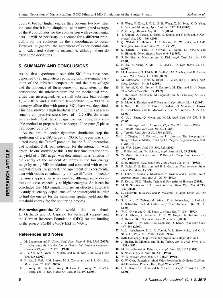
The averaged sputter yield from the IMD simulationsfor the energy range from 50 eV to 1 keV is compared inFigure 7 with the results from the ME simulations, withTRIM29 and TRIDYN30 MC simulations and with valuesfor the experimental sputter yield taken from the litera-ture. Experimental values for the low energy dependenceof the sputtering yield for SiC by Ar ions are rarely pub-lished. Mostly there are experimental results for light pro-jectiles like H, D, and He 51 because of its importancein the nuclear fusion technology. Because in literature noexperimental data have been found for the sputtering of aSiC (001) surface, the values for the sputter yield of SiC(0001) determined from target weight losses measured byan in-situ microbalance,52 by measuring the step height ofmesa structures with a microinterferometer53 and by Augerdepth profiling29 were chosen for comparison. However,Petzold et al. did not observe a dependence of the mea-sured sputter yield on the polytype of the substrate.
Up to 600 eV there is a good qualitative and quan-titative agreement between the ME values and the datafrom Comas and Cooper. Unfortunately they did notmeasure at higher energies. There is only one value of0.46 molecules/ion at 1 keV from Petzold available andTRIM and TRIDYN calculations, which are in the samerange. The experimental and TRIM values of Ecke et al.at 500 eV are a bit below those of Comas and of the MEsimulations. However it has to be kept in mind, that theyields of Ecke have been determined for 60� incidenceangle. Therefore in order to compare results obtained for60� incidence angle with those for 0�, the results for 60�
bombardment should be divided by the factor cos−f � withf as a fitting factor.54 Sigmund proposed the factor f to be5/3. Using this factor the experimental and the TRIM datapoints for 0� incidence, shown in Figure 7, have been cal-culated. Thus, there is some uncertainty due to a possibleunknown variation of this factor with energy. The averagedIMD data for the sputter yield show good agreement up to
0 100 200 300 400 500 600 700 800 900 1000
0.0
0.1
0.2
0.3
0.4
0.5
0.6 SiC(0001) exp.29
SiC(0001) exp.52
SiC(0001) exp.53
SiC(001) ME sim. (this work)SiC(001) IMD sim. (this work)SiC(001) TRIDYN sim.30
SiC(0001) TRIM sim.29
Spu
tter
yiel
d Y
in m
olec
ules
/ion
Ion energy in eV
Fig. 7. Comparison of experimental sputter yield values for SiC targetswith TRIM, TRIDYN and the present MD simulations.
J. Nanosci. Nanotechnol. 10, 1–9, 2010 7
RESEARCHARTICLE
Sputter Deposition of Nanocrystalline �-SiC Films and MD Simulations of the Sputter Process Ziebert et al.
300 eV, but for higher energy they become too low. Thisindicates that it is too simple to use an unweighted averageof the 9 coordinates for the comparison with experimentaldata. It will be necessary to account for a different prob-ability for the collisions on the 9 coordinates to occur.However, in general, the agreement of experimental datawith calculated values is reasonable, although there doexist some deviations.
5. SUMMARY AND CONCLUSIONS
As the first experimental step thin SiC films have beendeposited by rf magnetron sputtering with systematic vari-ation of the substrate temperature and the bias voltageand the influence of these deposition parameters on theconstitution, the microstructure and the mechanical prop-erties was investigated. At a small substrate bias voltageUs = −10 V and a substrate temperature Ts = 900 �C ananocrystalline film with pure �-SiC phase was deposited.This film showed a high hardness of H = 36 GPa at a rea-sonable compressive stress level of −2�2 GPa. So it canbe concluded that the rf magnetron sputtering is a suit-able method to prepare hard nanocrystalline pure �-phasehydrogen-free SiC-films.
As the first molecular dynamics simulation step thesputtering of a �-SiC-target at 700 K by argon was sim-ulated using the Tersoff potential for the Si–C interactionand tabulated ZBL pair potential for the interaction withargon. To our knowledge this is the first time that the sput-ter yield of a SiC target was determined as a function ofthe energy of the incident Ar atoms in the low energyrange by using MD simulations and compared with exper-imental results. In general, the agreement of experimentaldata with values calculated by the two different moleculardynamics approaches is reasonable, although some devia-tions do exist, especially at higher energies. So it can beconcluded that MD simulations are an effective approachto study the energy dependence of the sputter yield in orderto find the energy for the maximum sputter yield and thethreshold energy for the sputtering process.
Acknowledgments: We would like to thankU. Gerhards and D. Capriulo for technical support andthe German Research Foundation (DFG) for the fundingin the project SCHM 746/68-1/ZI 1174/3-1.
References and Notes
1. M. Lattemann and S. Ulrich, Surf. Coat. Technol. 201, 5564 (2007).2. H. Kleykamp, Bericht der Bunsen-Gesellschaft-Physical ChemistryChemical Physics 102, 1231 (1998).
3. J.-Y. Seo, S.-Y. Yoon, K. Niihara, and K. H. Kim, Thin Solid Films406, 138 (2002).
4. F. Liao, S. Park, J. M. Larson, M. R. Zachariah, and S. L. Girshick,Mater. Lett. 57, 1982 (2003).
5. B. Wang, W. Liu, G. J. Wang, B. Liao, J. J. Wang, M. K. Zhu,H. Wang, and H. Yan, Mater. Sci. Eng. B 98, 190 (2003).
6. B. Wang, Q. Zhao, J. C. Li, B. B. Wang, X. M. Song, X. D. Yang,H. Yan, and M. Wang, Appl. Surf. Sci. 217, 314 (2003).
7. Z. C. Feng, Microel. Eng. 83, 165 (2006).8. Y. Komura, A. Tabata, T. Narita, A. Kondo, and T. Mizutani, J. Non-crystal. Sol. 352, 1367 (2006).
9. Q. Wahab, L. Hultman, I. P. Ivanov, M. Willander, and J.-E.Sundgren, Thin Solid Films 261, 317 (1995).
10. S. Ulrich, T. Theel, J. Schwan, V. Batori, M. Scheib, andH. Ehrhardt, Diam. Relat. Mater. 6, 645 (1997).
11. S. Kerdiles, R. Madelon, and R. Rizk, Appl. Surf. Sci. 184, 150(2001).
12. E. Xie, Z. Zhang, Z. Ma, H. Li, and D. He, Opt. Mater. 23, 157(2003).
13. M. Lattemann, S. Ulrich, H. Holleck, M. Stueber, and H. Leiste,Diam. Relat. Mater. 11, 1248 (2002).
14. M. Lattemann, E. Nold, S. Ulrich, H. Leiste, and H. Holleck, Surf.Coat. Technol. 174, 365 (2003).
15. K. Pressel, G. G. Fischer, P. Zaumseil, M. Kim, and H. J. Osten,Thin Solid Films 294, 133 (1997).
16. T. Matsumoto, M. Kiuchi, M. Sugimoto, and S. Goto, Surf. Sci. 493,426 (2001).
17. H. Muto, S. Kamiya, and T. Kusumori, Opt. Mater. 23, 43 (2003).18. F. Neri, F. Barreca, E. Fazio, E. Barletta, G. Mondio, S. Trusso,
B. Brendebach, and H. Modrow, J. Vac. Sci. Technol. A 25, 117(2007).
19. G. Li, J. Zhang, Q. Meng, and W. Li, Appl. Surf. Sci. 253, 8428(2007).
20. F. H. Stillinger and T. A. Weber, Phys. Rev. B 31, 5262 (1985).21. J. Tersoff, Phys. Rev. Lett. 56, 632 (1986).22. J. Tersoff, Phys. Rev. B 39, 5566 (1989).23. J. F. Ziegler, J. P. Biersack, and U. Littmark, The Stopping and
Range of Ions in Matter, edited by J. F. Ziegler, Pergamon, New York(1985), Vol. 1.
24. M. V. R. Murty, Surf. Sci. 500, 523 (2002).25. J. P. Biersack and W. Eckstein, Appl. Phys. A 34, 73 (1984).26. W. Möller, W. Eckstein, and J. P. Biersack, Comp. Phys. Comm. 51,
355 (1988).27. D. E. Harrison, Crit. Rev. Solid State Mater. Sci. 14, S1 (1988).28. R. Smith, D. E. Harrison, and B. J. Garrison, Nucl. Instrum. Meth.
Phys. Res. B 46, 1 (1990).29. G. Ecke, R. Kosiba, V. Kharlamov, Y. Trushin, and J. Petzoldt, Nucl.
Instrum. Meth. Phys. Res. B 196, 39 (2002).30. R. Kosiba, Ph.D. Thesis, Technical University of Ilmenau (2005).31. M. H. Shapiro and P. Lu, Nucl. Instrum. Meth. Phys. Res. B 215,
326 (2004).32. L. Lutterotti, P. Scardi, and P. Maistrelli, J. Appl. Cryst. 25, 459
(1992).33. S. Ulrich, C. Ziebert, M. Stüber, P. Schloßmacher, H. Holleck,
E. Schweitzer, and M. Göken, Surf. Coat. Technol. 188–189, 331(2004).
34. W. C. Oliver and G. M. Pharr, J. Mater. Res. 7, 1564 (1992).35. G. J. Sibona, S. Schreiber, R. H. W. Hoppe, B. Stritzker, and
A. Revnic, Mat. Sci. Sem. Cond. Proc. 6, 71 (2003).36. J.-Y. Kim, B.-W. Lee, H.-S. Nam, and D. Kwon, Thin Sold Films
467, 294 (2004).37. V. I. Ivashchenko, P. E. A. Turchi, V. I. Shevchenko, and O. A.
Shramko, Phys. Rev. B 70, 115201 (2004).38. IMD Homepage, http://www.itap.physik.uni-stuttgart.de/∼imd.39. J. Stadler, R. Mikulla, and H. R. Trebin, Int. J. Mod. Phys. C 8,
1131 (1997).40. M. Parinello and A. Rahman, J. Appl. Phys. 52, 7182 (1981).41. S. Nose, J. Chem. Phys. 81, 511 (1984).42. W. G. Hoover, Phys. Rev. A 31, 1695 (1985).43. C. W. Gear, Numerical Initial Value Problems in Ordinary Differen-
tial Equations, Prentice Hall, EngleWood (1973).44. D. H. Kim, D. H. Kim, and K. S. Leem, J. Cryst. Growth 230, 285
(2001).
8 J. Nanosci. Nanotechnol. 10, 1–9, 2010
RESEARCHARTICLE
Ziebert et al. Sputter Deposition of Nanocrystalline �-SiC Films and MD Simulations of the Sputter Process
45. J. Samela, J. Kotakoski, K. Nordlund, and J. Keinonen, Nucl.Instrum. Meth. Phys. Res. B 239, 239 (2005).
46. F. Liao, S. L. Girshick, W. M. Mook, W. W. Gerberich, and M. R.Zachariah, Appl. Phys. Lett. 86, 171913 (2005).
47. A. Bolshakov and G. M. Pharr, J. Mater. Res. 13, 1049 (1998).48. V. Kulikovsky, V. Vorlícek, P. Bohác, A. Kurdyumov, and
L. Jastrabik, Diam. Relat. Mater. 13, 1359 (2004).49. J. Bohdansky, Nucl. Instr. and Meth. B 2, 587 (1984).
50. C. Garcia-Rosales, W. Eckstein, and J. Roth, J. Nucl. Mat. 218, 8(1994).
51. W. Eckstein, C. Garcia-Rosales, J. Roth, W. Ottenberger, SputteringData, Max-Planck-Institut für Plasmaphysik, Report IPP 9/82 (1993).
52. J. Comas and C. B. Cooper, J. Appl. Phys. 37, 2820 (1966).53. J. Pezoldt, B. Stottko, G. Kupris, and G. Ecke, Mat. Sci. Eng. B 29,
94 (1995).54. P. Sigmund, Phys. Rev. 184, 383 (1969).
Received: 14 November 2008. Accepted: 11 March 2009.
J. Nanosci. Nanotechnol. 10, 1–9, 2010 9