spin-polarized current-induced domain wall motion in cofeb
TRANSCRIPT

HAL Id: tel-01924456https://tel.archives-ouvertes.fr/tel-01924456
Submitted on 16 Nov 2018
HAL is a multi-disciplinary open accessarchive for the deposit and dissemination of sci-entific research documents, whether they are pub-lished or not. The documents may come fromteaching and research institutions in France orabroad, or from public or private research centers.
L’archive ouverte pluridisciplinaire HAL, estdestinée au dépôt et à la diffusion de documentsscientifiques de niveau recherche, publiés ou non,émanant des établissements d’enseignement et derecherche français ou étrangers, des laboratoirespublics ou privés.
Spin-polarized current-induced domain wall motion inCoFeB nanowires
Xueying Zhang
To cite this version:Xueying Zhang. Spin-polarized current-induced domain wall motion in CoFeB nanowires. Microand nanotechnologies/Microelectronics. Université Paris Saclay (COmUE), 2018. English. �NNT :2018SACLS104�. �tel-01924456�

Le mouvement des parois des domaines magnétiques dans le fil
de CoFeB induit par le courant polarisé
Spin-polarized current-induced domain
wall motion in CoFeB nanowires
Thèse de doctorat de l'Université Paris-Saclay préparée à Université Paris-Sud
École doctorale n°575 : electrical, optical, bio - physics and engineering (EOBE)
Spécialité de doctorat: Physique
Thèse présentée et soutenue à Orsay, le 15 Mai 2018, par
Xueying Zhang Composition du Jury : Vincent Jeudy Professeur, Université Paris-Saclay Président
Catherine Gourdon Directeur de recherche, Université Pierre et Marie Curie-Paris 6 Rapporteur
Vincent Repain Professeur, Université Paris Diderot – Paris 7 Rapporteur
Stefania Pizzini Directeur de recherche, Institut Néel Examinateur
Salim Mourad Chérif Professeur, Université Paris 13 Examinateur
Nicolas Vernier Maître de Conférence, HDR , Université Paris-Saclay Directeur de thèse
Weisheng Zhao Professeur, Université de Beihang Co-Directeur de thèse
NN
T :
20
18
SA
CL
S1
04

Université Paris-Saclay Espace Technologique / Immeuble Discovery Route de l’Orme aux Merisiers RD 128 / 91190 Saint-Aubin, France
I
Remerciements
Je souhaite commencer ce manuscrit par adresser mes remerciements sincères aux personnes qui
m’ont beaucoup aidé depuis quatre ans et qui ont contribué à l’achèvement de ce mémoire. Cette thèse a
été menée dans le cadre de la coopération entre le centre de nanoscience et nanotechnologie (C2N) de
l’Université Paris-Saclay et le Fert Beijing Institute de l’Université de Beihang.
Je voudrais tout d’abord adresser mes remerciements à mes directeurs de thèse Monsieur Nicolas
Vernier, Professeur à l’Université Paris-Saclay et Monsieur Weisheng Zhao, Professeur à l’Universié de
Beihang, qui m’ont accueilli dans leur équipe et qui m’ont soutenu tout au long des quatre ans de travail.
J’ai commencé des recherche sur le magnétisme en 2014 sous la direction de M. Weisheng Zhao, qui m’a
aidé à former des connaissance foundamentales sur le magnétisme, la spintronique et des méthode de
recherche via simulations micromagnétique. En 2015, je commence des recherches expérimentales sur
des parois du domaine magnétique sous la direction de M. Nicolas Vernier, qui a développé une
microscope de Kerr très puissant et qui m’a appris des techniques de microscopie de Kerr, des technologies
pour appliquer du champ magnétique et faire simultanément des tests électriques, des méthodes de
recherche expérimentales sur la paroi du domaine. Tous les résultats dans cette thèse ont été obtenus sous
la direction patiente de mes deux encadrants. Je tiens à les remercier également de m’avoir aidé à exploiter
des démarches de recherche scientifique et à résoudre des problèmes scientifiques ou administratifs.
Je voudrais aussi adresser mes remerciements à Monsieur Dafiné Ravelosona, professeur à
l’Université Paris-Saclay, qui m’a accueilli et qui m’a donné beaucoup de conseils précieux pendant la
recherche de la thèse.
Je voudrais ensuite remercier les membres de mon jury de leur temps consacré à ma thèse. Je remercie
particulièrement, mes rapporteurs professeurs Catherine Gourdon et professeur Vincent Repain pour le
regard critique et leurs remarques constructives sur mon travail. Je remercie également Professeur Vincent
Jeudy, professeur Stefania Pizzini, et professeur Mourad Cherif qui ont gentiment accepté d’examiner mes
travaux de thèse.
J’aimerais aussi adresser mes remerciements à Monsieur Laurent Vila, qui a aidé à concevoir et
fabriquer des nanostructures testées dans ce recherche, Monsieur Vincent Jeudy, qui m’a appris des
connaissance sur le mouvement de paroi dans le régime transition de dépiégeage et qui m’a aidé à analyser
des results expérimentals, Monsieur Bonan Yan, qui m’a appris à utiliser le logiciel Mumax3, Monsieur
Yue Zhang, avec qui nous avons conçu la mémoire de racetrack de forme annulaire, Monsieur Qunwen

II
Leng, qui m’a donné des conseils sur le design de la capteur à base de l’élasticité de paroi du domaine,
Monsieur Yu Zhang, pour les discussions sur des techniques de nano-fabrication et notre coopération sur
la recherche du renversement magnétique des nanodots.
Un grand merci à l'atelier du C2N. Grâce à leur travail scrupuleux et efficace, la fabrication et la mis
en place des appareil expérimentaux ont été possibles. Aussi, Je tiens à remercier tous mes collègues de
C2N et de l’Université de Beihang, de leur gentillesse et de leur accompagnement. Leurs conseils voire
les causeries menés pendant les déjeuners ou les pauses, qui ont beaucoup enrichi mes connaissances
profesionnelles ainsi que ma vie quotidienne. Cela a été un grand plaisir de travailler avec eux.
Naturellement, je voudrais aussi remercier tous mes amis chinois et français: Ping Che, Sylvain Eimer,
Gefei Wang, Qi An, Jiaqi Zhou, You Wang, Boyu Zhang, Chenghao Wang, Zhiqiang Cao... pour leur
accompagnement durant les quatre ans.
Un grand merci à China Scholarship Council (CSC) pour son support de financement pendent ma
recherche en France.
Enfin, je souhaite exprimer profonde gratitude à ma famille, dont notamment, mes parents, M. Cheng
Zhang et Mme Shuchun Wang, qui m’ont accompagné et soutenu sans condition depuis toujours.
III
Symbols
α: Damping constant
γ: Gyromagnetic ratio
γDW: DW surface energy
θSH: Spin Hall angle
μ: Exponent constant of the
creep law
μ0: Permeability of vacuum
μB: Bohr magneton
�⃗⃗� 𝑚: Magnetic moment
ξ: Non adiabatic constant
ρ: Resistivity
σ: Conductivity
𝜎 𝑆𝐻: Polarizing direction of
the spin Hall current
τ: Spin torque
χ: DW tilting angle
φ: Azimuthal angle of
magnetization
θ: Zenith angle of
magnetization
𝜙′: Kerr rotation
𝜙′′: Kerr ellipticity
ћ: Reduced Planck constant
Aex: Exchange stiffness
constant
B: Magnetic flux density
Bext: Externally applied field
D: DMI constant
e: Electric charge
Eex: Exchange energy
Ek: Anisotropy energy
Ed: Demagnetizing energy
EZeem: Zeeman energy
EDM: DMI energy
Fpin: Pinning force
g: Landau factor
H: Magnetic field
HDM: Effective DMI field
Hdemag: Demagnetizing field
Hext: Externally applied field
Hp_intr: Intrinsic pinning field
HK: Anisotropy field
Hdep: Depinning field
I: Electric current
j: Current density
jHM: Current density in heavy
metal layer
jSH: Spin Hall current density
jSTT: Current density for spin
transfer torque
KU: Uniaxial anisotropy
Keff: Effective anisotropy
field
kB: Boltzmann constant
l: Length
�⃗⃗� : Reduced magnetization
vector
�⃗⃗� 𝐷𝑊: Magnetic direction in
the center of DW
�⃗⃗� : Magnetization
MS: Saturation magnetization
P: Polarization ratio
Pγ: Laplace pressure
associated to DW surface
energy
Rcoil: Resistance of coil
t: Time
tM: Thickness of
ferromagnetic layer
T: Temperature
TC: Curie temperature
v: DW motion velocity
w: width

IV
Acronyms
AD-STT: Adiabatic Spin Transfer Torque
BLS: Brillouin Light Scattering
BW: Block Wall
DMI: Dzyaloshinskii-Moriya Interaction
DW: Domain Wall
FM: FerroMagnetic
FMR: FerroMagnetic Resonance
GMR: Giant MagnetoResistance
HM: Heavy Metal
MTJ: Magnetic Tunnel Junction
NA-STT: Non-Adiabatic Spin Transfer Torque
NW: Néel Wall
PMA: Perpendicular Magnetic Anisotropy
RM: Racetrack Memory
SAF: Synthetic AntiFerromagnetic
SH: Spin Hall
SHE: Spin Hall Effect
SOC: Spin-Orbit Coupling
SOI: Spin-Orbit Interaction
SOT: Spin-Orbit Torque
SQUID: Superconducting Quantum Interference Device
STT: Spin Transfer Torque
TMR: Tunneling MagnetoResistance
VSM: Vibrating Sample Magnetometer
1D model: One Dimension model

V
Contents
Abstract .......................................................................................................................................... 1
Résumé ........................................................................................................................................... 3
Chapter 1 Introduction .............................................................................................................. 5
Motivation ................................................................................................................................. 5
Organization of the thesis .......................................................................................................... 6
Chapter 2 State of the art ........................................................................................................... 7
Basics......................................................................................................................................... 7
Magnetic domain walls ........................................................................................................... 10
DW profile ........................................................................................................................ 10
DW surface energy ........................................................................................................... 11
DW dynamics .......................................................................................................................... 13
Field-driven DW motions ................................................................................................. 13
Spin transfer torque driven DW motion ........................................................................... 19
Spin orbit torque driven DW motion ................................................................................ 22
Micromagnetic simulations ..................................................................................................... 25
Applications of DW in storage, logic, communications and sensor ....................................... 25
DW based sensors ............................................................................................................ 26
Racetrack Memory ........................................................................................................... 27
Chapter 3 Experimental methods ............................................................................................ 29
Magneto-Optical Kerr effect ................................................................................................... 29
Typical optical circuits of Kerr microscopes ................................................................... 32
Configurations of the Kerr microscope for these studies ................................................. 35
Configurations of magnetic coils ............................................................................................ 36
Design of magnetic coils .................................................................................................. 37

VI
Power supply for the coil.................................................................................................. 43
Configurations for electrical tests ............................................................................................ 47
Samples and the measurements procedures ............................................................................ 49
Samples ............................................................................................................................ 49
Nucleation of DW ............................................................................................................ 50
Measurement of the DW velocity .................................................................................... 50
Chapter 4 Surface energy of domain walls ............................................................................. 52
Direct observation of the effect of DW surface tension and measurement of the domain wall
surface energy ....................................................................................................................................... 52
Spontaneous contraction of the magnetic bubble ............................................................. 52
The Laplace pressure of a bend DW ................................................................................ 54
Stabilization of the magnetic bubble and estimation of the DW surface energy ............. 55
Interactions of two magnetic domain bubbles .................................................................. 58
DW pinning and depinning at Hall crosses or at necks .................................................... 60
Precision of the DW surface energy measured using the two approaches ....................... 63
Magnetic sensors based on the DW surface tension ............................................................... 65
Concept and mechanism ................................................................................................... 65
Device design and simulations ......................................................................................... 66
Discussions ....................................................................................................................... 68
Conclusions ............................................................................................................................. 70
Chapter 5 Domain walls motion and pinning effects in nanowires ........................................ 71
Field-induced DWs motion in nanowires ................................................................................ 71
Randomly distributed hard pinning sites in nanowire ............................................................. 74
Experiments ...................................................................................................................... 74
Depinning field distribution ............................................................................................. 75
VII
Data analysis and the origin of the pinning effects .......................................................... 77
DW motion induced by the combined effect of magnetic fields and electric current ............. 79
Current-induced DW motion ............................................................................................ 79
DWs motion induced by synchronized current pulses and magnetic field pulses ........... 82
Polarization of CoFeB in the Ta/CoFeB/MgO structure .................................................. 86
Enhancement of DW pinning effects by spin hall current ...................................................... 88
Experiments and results.................................................................................................... 88
Influence of the SH current on the DW depinning process .............................................. 90
Comparison of the models with the experimental results ................................................ 97
Application: a ring-shaped racetrack memory based the complementary work of STT and SOT
............................................................................................................................................................... 98
Ring-shaped RM structure and configurations ................................................................. 99
Micromagnetic simulations ............................................................................................ 100
Results ............................................................................................................................ 100
Discussions ..................................................................................................................... 102
Conclusion ............................................................................................................................. 103
Chapter 6 General conclusions and perspectives .................................................................. 105
References .................................................................................................................................. 111
Appendices ................................................................................................................................. 127
Appendix 1: Mathematic demonstration of the expression of Laplace pressure in magnetism and
the associated DW behavior ................................................................................................................ 127
Appendix 2: Another example of magnetic sensors based on the elasticity of DWs .................. 133
Appendix 3: Experimental measurements of the resistivity of the CoFeB thin film .................. 135
Appendix 4: More information about the DW depinning field in Figure 5-22 ........................... 138
Appendix 5: List of publications during the doctoral research ................................................... 140
Résumé en français ..................................................................................................................... 141


1
Abstract
This thesis is dedicated to the research of the static and dynamic properties of magnetic Domain Walls
(DWs) in CoFeB nanowires. A measurement system based on a high-resolution Kerr microscope was
implemented and used for these research.
First, phenomena related to the DW surface tension was studied. A spontaneous collapse of domain
bubbles was directly observed using the Kerr microscope. This phenomenon was explained using the
concept of the Laplace pressure due to the DW surface energy. The surface energy of DW was quantified
by measuring the external field required to stabilize these bubbles. The DW pinning and depinning
mechanism in some artificial geometries, such as the Hall cross or the entrance connecting a nucleation
pad and a wire, was explained using the concept of DW surface tension and was used to extract the DW
surface energy. Benefited from these studies, a method to directly quantify the coefficient of
Dzyaloshinskii- Moriya Interactions (DMI) using Kerr microscope has been proposed. In addition, a new
type of magnetic sensor based on the revisable expansion of DW due to DW surface tension was proposed
and verified using micromagnetic simulations.
Second, the dynamic properties of DWs in Ta/CoFeB/MgO film and wires were studied. The velocity
of DW motion induced by magnetic fields or by the combined effect of synchronized magnetic field pulses
and electrical current pulses was measured. In steady flow regime, the velocity of DW motion induced by
the combined effect of the field and the current equals to the superposition of the velocities driven by field
or current independently. This result allowed us to extract the spin-polarization of CoFeB in this structure.
Pinning effects of DW motion in narrow wires was studied. Depinning fields of hard pinning sites for the
field-driven DW motion in nanowires was measured. It was found that the pinning effects become severer
as the width w of the wires scaled down. A linear relationship between the depinning field and w was
found. The origin of these hard pinning sites, as well as their influences on the DW motion velocity, was
discussed. Furthermore, it was found that the pinning effect was enhanced when a current was applied, no
matter the relative direction between the DW motion and the current. We propose a possible explanation,
which would be an effect of the spin Hall current from the sublayer (Ta). Although there was no DMI or
in-plane field, the spin Hall current, which was polarized in the transverse direction, can still exert a torque
on the Bloch DW, once the DW tilts away from the transverse direction.
At last, a ring-shaped racetrack memory based on the combined work of STT and has been proposed.
Compared with the traditional line-shaped racetrack memory, this ring-shaped memory allows the DW

2
moving in a ring-shaped nanowire and the data dropout problem can be avoided. The design and
optimization work was performed with micromagnetic simulations.
Keywords: Domain Wall (DW), Kerr microscopy, CoFeB, Surface tension, Pinning effect, Spin
transfer torque (STT), Spin-orbit torque (SOT), racetrack memory, magnetic sensor, Magnetism,
Spintronics

3
Résumé
Cette thèse est consacrée aux recherches des propriétés statiques et dynamiques des parois de
domaines magnétiques (DW pour Domain Wall) dans les nanofils CoFeB. Un système de mesure basé sur
un microscope Kerr à haute résolution a été mis en place et utilisé pour ces recherches.
Tout d'abord, les phénomènes liés à la tension interfaciale des parois ont été étudiés. La contraction
spontanée des bulles de domaine a été observée directement en utilisant le microscope Kerr. Ce
phénomène a été expliqué en utilisant le concept de la pression de Laplace due à l'énergie interfaciale des
parois. L'énergie interfaciale des parois a été quantifiée en mesurant le champ externe nécessaire pour
stabiliser ces bulles. Le mécanisme de la piégeage et de la dépiégeage des parois dans certaines géométries
artificielles, comme la croix de Hall ou l'entrée reliant un carré de nucléation et un fil, a été expliqué en
utilisant le concept de tension interfaciale des parois et a été utilisé pour extraire l'énergie interfaciale des
parois. Bénéficiant de ces études, une méthode permettant de quantifier directement le coefficient des
Interactions de Dzyaloshinskii- Moriya (DMI pour Dzyaloshinskii- Moriya Interaction) à l'aide du
microscope Kerr a été proposée. En outre, un nouveau type de capteur magnétique basé sur l'expansion
réversible de paroi en raison de la tension interfaciale a été proposé et vérifié en utilisant des simulations
micromagnétiques.
Deuxièmement, les propriétés dynamiques des parois dans le film et les fils Ta / CoFeB / MgO ont
été étudiées. La vitesse du propagation des parois induite par le champ magnétique ou par l'effet combiné
des impulsions de champ magnétique synchronisées et des impulsions de courant électrique a été mesurée.
En régime précessionne, la vitesse du mouvement DW induite par l'effet combiné du champ et du courant
est égale à la superposition des vitesses entraînées par le champ ou le courant indépendamment. Ce résultat
nous a permis d'extraire la polarisation de spin de CoFeB dans cette structure. Les effets de piégeage du
mouvement des parois dans les fils étroits ont été étudiés. Des champs de dépiégeage associés aux gros
défauts pour le mouvement des parois induit par champ dans les nanofils a été mesurée. Il a été constaté
que les effets de piégeage deviennent plus sévères lorsque la largeur w des fils diminue. Une relation
linéaire entre le champ de piégeage et 1/w a été trouvée. L'origine de ces sites d'ancrage durs ainsi que
leurs influences sur la vitesse de mouvement des parois ont été discutées. En outre, il a été constaté que
l'effet d'épinglage était amélioré lorsque le courant était appliqué, quelle que soit la direction relative entre
le mouvement des parois et le courant. Cet accroissement pourrait être expliqué par l'effet du courant de
Hall de spin de la sous-couche (Ta). Bien qu'il n'y ait pas eu de DMI ou de champ planaire, le courant de

4
Hall de spin, polarisé dans la direction transversale, peut exercer un couple sur la parois de type de Bloch,
une fois que la paroi s'éloigne de la direction transversale.
Enfin, un dispositif mémoire de circuit en forme d'anneau basée sur le travail combiné de STT et SOT
a été proposée. Comparée à la mémoire de piste traditionnelle en forme de ligne, cette mémoire en forme
d'anneau permet au paroi de demaine de se déplacer dans un nanofil en forme d'anneau sans être éjecté,
évitant ainsi la perte des informations associées. Le travail de conception et d'optimisation a été réalisé
avec des simulations micromagnétiques.
Mots clés: Paroi de domaine magnétique, Microscopie Kerr, CoFeB, Tension interfaciale, Effet de
piégeage de paroi de domaine, Couple de transfert de spin, Couple d'orbite à spin, Mémoire de type
Racetrack, Capteur magnétique, Magnétisme, Spintronique

CHAPTER 1 INTRODUCTION
5
Chapter 1 Introduction
Motivation
Magnetic domains and Domain Walls (DWs) are very common objects in the magnetic material.
Static and dynamic properties of DWs have always been one of the central research topics of magnetism
in the last hundred years. On the one hand, these researches provide varieties of ways to characterize the
basic properties of the magnetic material or magnetic structures. For example, by analyzing the state or
the behavior of DWs, some parameters such as the saturation magnetization 𝑀𝑆[1], the exchange stiffness
𝐴𝑒𝑥 [2–4], the strength of Dzyaloshinskii-Moriya Interactions (DMIs) [5] etc. can be quantified.
On the other hand, varieties of devices based on DWs have been proposed or developed for
information processing, storage, and transport. For example, DWs based logic devices[6,7], DWs based
Artificial Neural Networks (ANNs) computing[8–10], DW as the transmission channel of spin wave[11]
etc. In particular, the prototype of Racetrack Memory (RM) proposed by S. Parkin[12,13], which stores
the information using the flowing DWs in nanowires, triggered a sustained boom of the research on DWs
motions in nanowires.
In the last two decades, varieties of emergent phenomena have been involved into the DW related
phenomena. For example, different from the traditional field-induced DW motion, it was found that DWs
could be moved in narrow wires by electrical current via spin transfer torque (STT). Owing to the DMI
and Spin Hall effect (SHE), DWs can be moved by the spin-orbit torque (SOT) with an ultra-fast speed.
In structures with perpendicular magnetic anisotropy (PMA), DWs with a smaller width were obtained.
Some emergent materials have been widely explored to develop magnetic based devices, such as
CoFeB[14–18], which has a low damping and a low depinning field, promising a better efficiency for DW
based devices. All these developments provide chances for a better understanding of the underlying
physical phenomena or for the development of novel DWs based devices.
The DW motion in nanowires with the heavy metal/CoFeB/MgO structure is very interesting in view
of its potential applications for DW based device for information storage or processing. However, many
underlying issues need to be better understand. The current-induced DW motion needs to be further
studied because, in this system, many effects are potentially involved, such as the adiabatic STT (AD-
STT), non-adiabatic STT (NA-STT), the Spin-Orbit Coupling (SOC), the SHE etc. The role of these
various effects on the DW motion needs to be clarified.
CHAPTER 1 INTRODUCTION
6
Therefore, this thesis focus on the studies of static and dynamic properties of DWs in the CoFeB
nanowires, including the basic parameters such as the DW surface energy, the current and field-induced
DW motion velocities and the pinning effects.
Organization of the thesis
This thesis is organized into six chapters, including the introduction and the conclusion.
In chapter 2, the state of the art concerning to this thesis is introduced. We generally summarize the
basic theory related to DWs, including the static properties such as DW surface energy, the dynamic
properties such as the DW motion driven by field or current, the interest to study DWs and their
applications.
In chapter 3, study methods of this thesis is introduced. This chapter includes the following contents:
the configuration of a high resolution Kerr microscope; the design of magnetic coils, which are capable to
nucleate a DW and to measure the DW velocity in a microstructure; the configuration of electric tests; the
nature of the sample studied and the method to measure the DW velocity etc.
In chapter 4, we present the research on the DW surface tension. A series of experiments in which
the DWs surface tension play the dominant role are introduced, including the stabilization of magnetic
bubbles, the depinning of DW at artificial geometries. The Laplace pressure is used to explain these
phenomena. The design and verification of sensors based on the DW surface energy are introduced.
In chapter 5, experiments about the field and current-driven DW motion in CoFeB nanowires are
introduced. The velocity of the field-driven DW motion, as well as the velocity of the DW motion driven
by the combined effects of magnetic field and electrical current are measured and analyzed. The DW
pinning effect in the nanowire and its dependence on the width of wires and on the applied current are
studied. At last, a ring-shape racetrack memory based on the complementary work of STT and SOT is
proposed and verified using micromagnetic simulations.

CHAPTER 2 STATE OF THE ART
7
Chapter 2 State of the art
Basics
In this thesis, we shall use exclusively the units and definitions of the Système International (S.I.).
The strength of the magnetization of a FerroMagnetic (FM) material is defined as the quantity of
magnetic moments per unit volume[19],
�⃗⃗� =𝑑�⃗⃗� 𝑚
𝑑𝑉 (2-1)
where 𝑑�⃗⃗� 𝑚 is the elementary magnetic moment, with a dimension of A ∙ 𝑚2, and dV is the volume
element. Magnetic moments may be contributed by the motion of the electrons in atoms, the spin of
electrons and the spin of nuclei. However, the contribution from the spin of electrons are the major one[19].
The stable state of a magnetic system is determined by the equilibrium of different energy terms
involved, including the exchange energy Eex, the crystalline anisotropy energy EK, the magnetostatic
energy Ed (or demagnetizing energy) originated from the dipole-dipole interaction, and the Zeeman energy
EZeem when an external field is applied etc.
Exchange interactions:
Benefited from the development of the quantum theory, W. Heisenberg constructed a model in 1926-
1928, which explained the origin of the magnetism in the magnetic material, namely, the Heisenberg
exchange interaction model[20]. A simple understanding of this model is: the unpaired spins in nearby
atoms tend to align in parallel to reduce the electrostatic energy (i.e. energy associated with the Coulomb
interaction). This interaction is very strong, orders of magnitude larger than any other interaction such as
the dipole-dipole interaction. However, the exchange interaction diminishes rapidly as the distance of
spins increases. The result is that the magnetization in a small range is aligned.
Microscopically, the energy aroused by this interaction can be written as[19],
𝐸𝑒𝑥 = ∫𝑒𝑒𝑥𝑑𝑉 = 𝐴𝑒𝑥 ∫(𝑔𝑟𝑎𝑑 �⃗⃗� )2𝑑𝑉 (2-2)
Where �⃗⃗� is the magnetization vector, defined as �⃗⃗� = �⃗⃗� 𝑀𝑆⁄ with MS the saturation magnetization,
and Aex is the exchange stiffness, with a dimension of J/m. Aex is an intrinsic property of the material and
it changes with the temperature [21].
Conventionally, the coordinate shown in Figure 2-1 is used to describe the magnetization direction,
�⃗⃗� = (sin 𝜃 cos𝜑 , sin 𝜃 sin𝜑 , cos 𝜃) (2-3)

CHAPTER 2 STATE OF THE ART
8
Then we have
𝑒𝑥 = 𝐴𝑒𝑥[(𝑔𝑟𝑎𝑑𝜃)2 + sin2𝜃 (𝑔𝑟𝑎𝑑𝜑)2] (2-4)
Anisotropy energy
The magnetization direction in ferromagnetic material usually tends to align parallel to some
specified axis, depending on the crystalline structure. The associated energy is called the anisotropy energy.
The anisotropy energy (excluding the shape anisotropy) basically comes from the spin-orbit interaction
(SOI)[21].
In the case of uniaxial anisotropy, the magneto-crystalline energy is described by a polynomial
development in sinθ with only even terms for reasons of symmetry in the thin films studied,
𝑒𝐾𝑉= 𝐾𝑉1𝑠𝑖𝑛
2𝜃 + 𝐾𝑉2𝑠𝑖𝑛4𝜃 (2-5)
KV1 and KV2 are the first and second order anisotropy constants. In general, KV1 is much larger than
KV2. A positive KV1 favors that the material has an easy axis while a negative KV1 favors an easy plane
perpendicular to the anisotropy axis.
A perpendicular magnetic anisotropy (PMA) can be obtained in the ultra-thin multilayers structure
due to the reduced symmetry of the atomic environment in the surface. The surface anisotropy was first
introduced by Néel in 1953. Supposing that the surface is in the x-y plane, the surface anisotropy energy
density is expressed as[21],
𝑒𝑠 = 𝐾𝑠[1 − (�⃗⃗� ∙ �⃗� )2] = 𝐾𝑠 sin2 𝜃 (2-6)
Where �⃗� is the surface normal. 𝐾𝑠 has a dimension of 𝐽/𝑚2 and is in the order of 10−4 to 10−3𝐽/𝑚2.
This term becomes the predominant effect beyond the crystalline anisotropy only when the thickness of
Figure 2-1 Sketch of the default coordinate and symbol of angle used in this thesis.
z
x
y
m
plane of the film
θ

CHAPTER 2 STATE OF THE ART
9
the ferromagnetic layer becomes very thin (~1 nm) and leads to the PMA in the ultra-thin multilayers
structure. The material studied in this thesis has such an anisotropy.
Zeeman energy
For magnetic moment �⃗⃗� 𝑚 in a magnetic field �⃗� , �⃗⃗� 𝑚 tends always to stay in parallel with �⃗� . The
associated potential energy is 𝐸𝑀 = −�⃗⃗� 𝑚 ∙ �⃗� . The Zeeman energy indicates the magnetic energy
introduced when an external field �⃗� 𝑒𝑥 is applied to a magnetic material, expressed as,
𝐸𝑍 = −∫ �⃗� 𝑒𝑥 ∙ �⃗⃗� 𝑑𝑉 (2-7)
Magneto-static energy
Inside a magnetic material, the magnetic flux density �⃗� , the magnetic field intensity �⃗⃗� and the
magnetization �⃗⃗� have the following relationship[21],
�⃗� = 𝜇0(�⃗⃗� + �⃗⃗� ) (2-8)
Where 𝜇0 is the permeability of vacuum. According to Maxwell’s equation,
𝑑𝑖𝑣�⃗� = 𝜇0𝑑𝑖𝑣(�⃗⃗� + �⃗⃗� ) = 0 (2-9)
So
𝑑𝑖𝑣�⃗⃗� = −𝑑𝑖𝑣�⃗⃗� (2-10)
If there is no current nor alternating electric field,
𝑟𝑜𝑡(�⃗� ) = 0 (2-11)
Combining these equations with the boundary condition, we can find that the magnetic field outside
a magnet is not zero. This field is conventionally called the stray field. A magnetic field opposite to the
magnetization inside the magnet exists. This field H is called the demagnetizing field.
In fact, the stray field and the demagnetizing field has the same origin. The different appellations
depend on how to define the studied magnetic element. Here we use the symbol �⃗⃗� 𝑑 as an indication. The
associated energy, which is usually called the magneto-static energy, the stray field energy or the
demagnetizing energy, is[21]
𝐸𝑑 =1
2𝜇0 ∫ �⃗⃗� 𝑑
2𝑑𝑉
𝑎𝑙𝑙 𝑠𝑝𝑎𝑐𝑒= −
1
2𝜇0 ∫ �⃗⃗� 𝑑�⃗⃗� 𝑑𝑉
𝑠𝑎𝑚𝑝𝑙𝑒 (2-12)
The calculation of this energy is very complex. References [21] gives several methods for the
calculation of the demagnetizing energy. In particular, the density of demagnetizing energy in an infinite
thin film with a uniform magnetization can be expressed as,

CHAPTER 2 STATE OF THE ART
10
𝑒𝑑 = −1
2𝜇0𝑀𝑆
2sin2𝜃 (2-13)
This contribution favors an easy plane anisotropy, and a hard out-plane direction for the
magnetization. The energy due to the demagnetization field is often called shape anisotropy.
Regarding the uniaxial anisotropy due to the crystalline as described in Eq. (2-5) and the surface
anisotropy described in Eq. (2-6), neglecting the second order, one can describe the uniaxial anisotropy
energy as [22],
𝑒𝐾 = 𝐾𝑈 sin2 𝜃 (2-14)
with 𝐾𝑈 = 𝐾𝑉1 + 𝐾𝑆. If we further consider into the shape anisotropy described in Eq. (2-13), we can
get an effective anisotropy energy density[22],
𝑒𝐾,𝑒𝑓𝑓 = 𝐾𝑒𝑓𝑓 sin2 𝜃 (2-15)
With,
𝐾𝑒𝑓𝑓 = 𝐾𝑈 −1
2𝜇0𝑀𝑆
2 (2-16)
Dzyaloshinskii-Moriya interactions
Dzyaloshinskii-Moriya interactions (DMI) have been intensively studied in recent years. The DMI
exists in the material in which the structure reversion symmetry is broken. The energy density associated
with this interaction is[23],
𝑒𝐷𝑀 = 𝐷[𝑚𝑧div�⃗⃗� − (�⃗⃗� ∙ ∇⃗⃗ )𝑚𝑧] (2-17)
where D is DMI constant. Although DMI is negligible in the sample we have studied, the result presented
in this work opens a new way to study DMI, as it will be seen at the end of this manuscript.
Magnetic domain walls
DW profile
Below a critical temperature (called Curie temperature), the magnetization in adjacent zone tends to
spontaneously align in parallel due to the exchange integration in ferromagnetic material. The region in
which the magnetization is in a uniform direction is called magnetic domain. Magnetic Domain Wall (DW)
is the interface separating two domains in the magnetic material. In a static state, the configuration of a
DW is determined by the equilibrium under the competition of different energy terms. Properties of DWs,
including the arrangement of the magnetization, the DW width, and the surface energy, can be calculated

CHAPTER 2 STATE OF THE ART
11
by minimizing the free energy of the system. For example, the DW tends to stay in a Bloch Wall (BW)
configuration in an infinite film or a wire (only when wire width is larger than DW width) with PMA and
without DMI, because this configuration can minimize the demagnetizing energy. In a material with strong
DMI, the DW is stabilized in a Néel Wall (NW) configuration because this type of DW can minimize the
energy associated to the DMI[24].
Based on the 1D model (supposing that the magnetization is identical in the transverse direction, i.e.
y-direction in Figure 2-1) and by minimizing the energy of the system, one can deduce a function to
describe the rotation of the magnetization of a DW,
𝜃(𝑥) =𝜋
2− 2arctan (𝑒
𝑥−𝑥0∆ ) (2-18)
Where x0 is the center position of the DW. The DW width is ∆= √𝐴𝑒𝑥 𝐾𝑒𝑓𝑓⁄ for BW in static state.
Note that this width is defined by Thiele and is conventionally called the Thiele width. The geometrical
width of the DW in this case is πΔ[25]. For a NW, A. Thiaville et al. numerically calculated the DW width
when DMI exists [23] and found that the width of NW is larger than the BW. The increase of DW width
is caused by the magnetostatic field.
DW surface energy
After determining the DW profile by minimizing the total free energy, one can obtain the DW energy
per unit surface (i.e. surface energy). For a BW [23],
γ𝐵𝑊 = 4√𝐴𝑒𝑥𝐾𝑒𝑓𝑓 (2-19)
If DMI or an in-plane field Hx exist, the expression of the DW surface energy becomes complex [5],
𝛾𝐷𝑊 = {𝛾BW −
𝜋2∆𝑀𝑆2
8𝐾𝐷(𝐻𝑥 + 𝐻𝐷𝑀)2 𝑓𝑜𝑟 |𝐻𝑥 + 𝐻𝐷𝑀| <
4𝐾𝐷
𝜋𝑀𝑆
𝛾BW + 2𝐾𝐷 − 𝜋∆𝑀𝑆|𝐻𝑥 + 𝐻𝐷𝑀| 𝑜𝑡ℎ𝑒𝑟𝑤𝑖𝑠𝑒 (2-20)
where KD is the demagnetizing energy of DWs and HDM is the effective field due to DMI.
In particular, for a pure NW fixed only by the DMI,
γ𝐷𝑊 = 4√𝐴𝑒𝑥𝐾𝑒𝑓𝑓 − πD (2-21)
Note that this energy is defined with respect to the energy in the uniformly magnetized state.
A conventionally used method to experimentally quantify the DW surface energy is by observing the
domain structure in the demagnetizing state[2,3]. As shown in Figure 2-2, in the demagnetizing state, the
magnetic texture of thin film with PMA is of a labyrinthine like distributed stripes. This state is mainly
the competition result of the demagnetizing energy and the DW surface energy. The characteristic period

CHAPTER 2 STATE OF THE ART
12
wp of the domain can be obtained after analyzing the images. Then, the DW surface energy can be deduced
using the following formula developed by Kaplan and Gehring[26],
𝑤𝑝 = 1.91𝑡𝑀𝑒𝑥𝑝(𝜋𝑤0/𝑡𝑀) (2-22)
where 𝑡𝑀 is the thickness of the FM layer and,
𝑤0 = γ𝐷𝑊/𝜇0𝑀𝑆2 (2-23)
However, the accuracy of the results obtained via this method depends on how the demagnetizing
state is obtained. Usually, the as-prepared sample is in a naturally demagnetized state. However, once
magnetized, it is difficult to return to the intrinsic demagnetized state, even after a demagnetizing process
via an alternating and exponentially decaying magnetic field, as done in the above example (Figure 2-2).
When the alternating field decays to a low value, the motion of the DW is usually trapped by the defects,
one can never know how close the magnetization approaches the intrinsic demagnetizing state. Therefore,
a more direct and accurate method to quantify the DW surface energy is desired.
The DW surface energy is a very important and fundamental parameter which affects the DW
behaviors. A surface tension exists due to this energy. In some literature, this effect is also called as the
DW elasticity[27,28]. For example, the DW depinning before pinning sites is determined by the
competition between several energy terms such as the pinning barrier, the DW surface energy, and the
Zeeman energy[29]. Another example, the stabilization of the domain bubble, the skyrmions are also
affected by the DW surface energy.
Figure 2-2 Fig. 2. MOKE microscope images of domain structures. Sample:
Ta(5nm)/Co20Fe60B20(t)/MgO(1)/Ta(2). (a)–(c) sample A (as deposited, t=1.1), and
(d)–(f) sample B (annealed, t=1.3) in demagnetized state at different temperatures (10,
200, and 300 K). Extracted from [IEEE MAGNETICS LETTERS, Volume 2 (2011)].

CHAPTER 2 STATE OF THE ART
13
DW dynamics
DW can be moved or manipulated through varieties of mechanism, for example, by an external
magnetic field, by the STT, by the SHE current, by the an electric field[30–32], by the spin wave[33–37],
by the polarized light[38] or by the thermal gradient[39]. Among them, the first three mechanisms were
most studied.
Field-driven DW motions
Field-driven DW motions predicted by the 1D model
First, we consider the DW motion in a defect-free sample. In this case, as predicted by the one
dimension model (1D model), the DW motion can be divided into three regimes: the steady regime for H
between 0 and the Walker breakdown field HW, the intermediate regime after Walker breakdown and the
precessional regime[40], as shown in Figure 2-3(a).
When the applied field is smaller than a critical value, the DW motion is in a steady regime, also
called the viscous regime. The magnetization in the center of the DW �⃗⃗� 𝐷𝑊 rotates in the plane such that
the azimuth angle 𝜑(𝐻𝑒𝑥𝑡) (defined as the angle between and the longitudinal direction, as shown in
Figure 2-1) is constant. The DW velocity is proportional to the magnitude of the applied field Hext[41,42],
𝑣 =𝛾𝛥𝜑(𝐻𝑒𝑥𝑡)
𝛼𝜇0𝐻𝑒𝑥𝑡 (2-24)
where 𝛾 is the gyromagnetic ratio, α is the damping parameter (note that the constant can be
obtained through different experiments. But, there is not yet agreement between them, values obtained
through ferromagnetic resonance are quite different from the one obtained through DW propagation. It
Figure 2-3 (a) ) Regimes of domain-wall flow motion in an ideal ferromagnetic film without pinning.
(b)Theoretical variation of the velocity, v, of a 1D interface (domain wall) in a 2D weakly
disordered medium submitted to a driving force, f (magnetic field, H), at zero and finite temperature,
T. The creep, depinning, and flow regimes are labeled. Extracted from [PRL 99, 217208 (2007)].
CHAPTER 2 STATE OF THE ART
14
suggested that locally induced anisotropy due to structural relaxation and roughness increased the damping
related to the DW motion [43,44]). 𝛥𝜑(𝐻𝑒𝑥𝑡) is the DW width parameter taking into consideration of the
demagnetizing field, which changes with 𝜑(𝐻𝑒𝑥𝑡),
𝛥𝜑(𝐻) = √𝐴
𝐾𝑒𝑓𝑓+1
2𝜇0𝑀𝑆
2𝑐𝑜𝑠2𝜑 (2-25)
Here, 𝐾𝑒𝑓𝑓 is the effective anisotropy field including the magneto-static field, as defined by Eq.
(2-16).
When the external field reaches a critical field, namely, the Walker breakdown field, the rotation of
�⃗⃗� 𝐷𝑊 reaches π/2. After the Walker breakdown, the DW velocity drops rapidly because of the collective
precession of the DW magnetization. The Walker breakdown field 𝐻𝑊 is directly related to α[45],
𝐻𝑊 = 𝛼𝑀𝑆/2 (2-26)
After the external field has exceeded the Walker breakdown field, the DW moves in a precessional
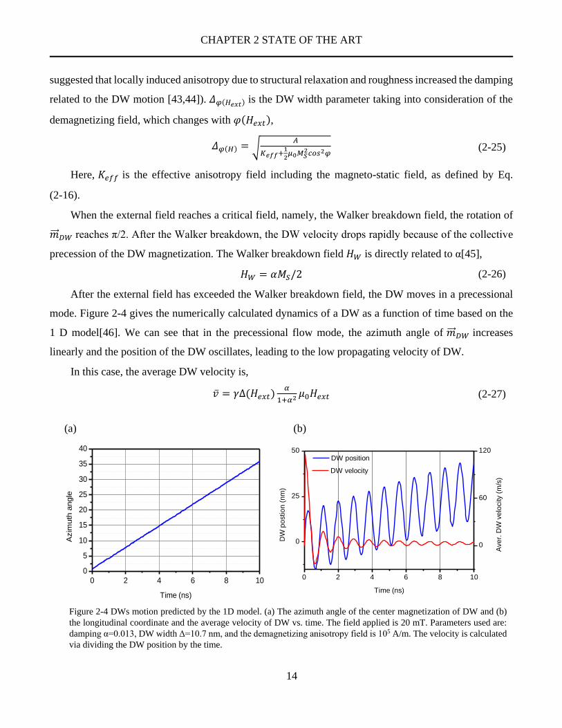
mode. Figure 2-4 gives the numerically calculated dynamics of a DW as a function of time based on the
1 D model[46]. We can see that in the precessional flow mode, the azimuth angle of �⃗⃗� 𝐷𝑊 increases
linearly and the position of the DW oscillates, leading to the low propagating velocity of DW.
In this case, the average DW velocity is,
�̅� = 𝛾Δ(𝐻𝑒𝑥𝑡)𝛼
1+𝛼2 𝜇0𝐻𝑒𝑥𝑡 (2-27)
0 2 4 6 8 10
0
5
10
15
20
25
30
35
40
Azim
uth
angle
Time (ns)
0 2 4 6 8 10
0
25
50
0
60
120 DW position
DW
po
stio
n (
nm
)
Time (ns)
DW velocity
Ave
r. D
W v
elo
city (
m/s
)
(a) (b)
Figure 2-4 DWs motion predicted by the 1D model. (a) The azimuth angle of the center magnetization of DW and (b)
the longitudinal coordinate and the average velocity of DW vs. time. The field applied is 20 mT. Parameters used are:
damping α=0.013, DW width Δ=10.7 nm, and the demagnetizing anisotropy field is 105 A/m. The velocity is calculated
via dividing the DW position by the time.
CHAPTER 2 STATE OF THE ART
15
Field-driven DW velocity in 2D films with defects
DW pining in infinite film
As a matter of fact, the magnetic film is not perfect. Some pinnings exist, which may arise from
nanoscale defects such as atomic steps, grain boundaries[47], surface roughness, local variations of the
thickness/composition[29,48], variation in stress, etc., leading to random fluctuations of the anisotropy or
of the exchange interaction.
When the moving DW comes across a pinning site in the film, it may get over the pinning site through
two regimes: (1) if the pinning site is strong enough so that the DW cannot get over the energy barrier
directly, or if the distance between the two pinning sites is large enough, the DW may keep propagating
on the left and the right of the site, until it has completely surrounded the sites, which disappear at last. (2)
If the applied field is strong enough or if the pinning is not solid enough, the DW directly overcomes the
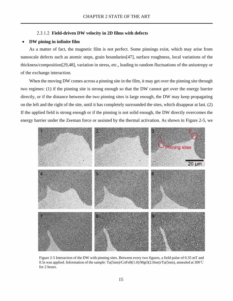
energy barrier under the Zeeman force or assisted by the thermal activation. As shown in Figure 2-5, we
Figure 2-5 Interaction of the DW with pinning sites. Between every two figures, a field pulse of 0.35 mT and
0.5s was applied. Information of the sample: Ta(5nm)/CoFeB(1.0)/MgO(2.0nm)/Ta(5nm), annealed at 300℃
for 2 hours.

CHAPTER 2 STATE OF THE ART
16
have directly observed these two processes using a Kerr microscope. In the field of vision, two hard
pinning sites appeared and they induced the curvature of the propagating DW. The DW passed the pinning
site 2 after reaching a short radius of curvature. However, the DW cannot go over the pinning site 1. At
last, an unreversed domain stripe was formed. In fact, many strips of this kind can be found after the weak
0,46 mT x 480 s 0,53 mT x 840 s 0,59 mT x 300 s
0,93 mT x 5 s 1,11 mT x 0,5 s 1,78 mT x 0,03 s
Figure 2-7Morphology of domains propagations under different fields, observed with a Kerr microscope. Information of the
sample: Si/SiO2/5Ta/40CuN/5Ta/1.1Co40Fe40B20/1MgO/5Ta, annealed at 380°C during 20 minutes.
Figure 2-6 (a) DW propagation after a field pulse of 0.4mT and 30s. (b) DW propagation after a pulse of
3.1 mT and 0.2 ms. (c) the white lines denotes the disappeared domain stripes under the pressure of the
field of 2.8 mT. Information of the sample: Ta(5nm)/CoFeB(1.0)/MgO(2.0nm)/Ta(5nm), annealed at 300℃
for 2 hours.

CHAPTER 2 STATE OF THE ART
17
field-induced propagation of DWs, as shown in Figure 2-6 (a) and Figure 2-7. In Figure 2-6, we have done
a comparison of the morphology of reversed domains after a weak field with that after a strong field. The
unreversed domain stripes began to merge as the applied field increased to a critical value (about 2.8 mT
in this sample). The distance of these strips can be used to estimate the magnetization of the material[1].
In the case when the defects in a sample are strong or when the driving field is relatively small, the trace
of DWs propagation is dendritic, as shown in Figure 2-7. When the applied field increases, the edge of
expanded domains becomes smoother.
DW motion in creep regime
In ultra-thin magnetic films, the interaction of DWs with the random disorder at low magnetic fields
leads to the well-known creep theory[29,49,50], which describes the motion of a 1D interface in a 2D
random disorder. The DW velocity can be expressed as[29,50],
𝑣 = 𝑣0exp [− (𝑈𝑐
𝑘𝐵𝑇) (
𝐻𝑝_𝑖𝑛𝑡𝑟
𝐻)𝜇] (2-28)
Where UC is a parameter to characterize the strength the energy barriers due to defects in a material,
𝑘𝐵 is the Boltzmann constant, T is the temperature, 𝑣0 is constant related to the properties of material with
a dimension of velocity, and μ is a constant. For the DW motion in a 2D system, 𝜇 = 1/4. 𝐻𝑝_𝑖𝑛𝑡𝑟 is called
the intrinsic pinning field of a material. The theory of creep regime applies from zeros field until 𝐻𝑝_𝑖𝑛𝑡𝑟.
0.4 0.6 0.8 1.0 1.2
1E-4
1E-3
0.01
0.1
1
10
Exp. result
Linear fitting
DW
velo
city (
m/s
)
(μ0H
app)-1/4
(mT-1/4
)
μ0H
p_intr=3.01 mT
Figure 2-8 Field-induced DW motion velocity in creep regime, in this measurement, the
temperature is 24°C. Information of the sample: Ta(5nm)/CoFeB(1.0)/MgO(2.0nm)/Ta(5nm),
annealed at 300°C for 2 hours.

CHAPTER 2 STATE OF THE ART
18
According to Eq. (2-28), a linear relationship can be found between ln(v) and H-1/4. As an example,
we show here the measured DW velocity on the sample we have studied in this thesis and the fitting result
with the creep law, as shown in Figure 2-8. We can see that the measurement results get a good agreement
with the prediction of Eq. (2-28). The intrinsic pinning field 𝜇0𝐻𝑝_𝑖𝑛𝑡𝑟 of the sample is extracted to be
about 3 mT.
In addition, the dependence of the field-induced velocity on the temperature in creep mode has also
been examined in this sample, as shown in Figure 2-9.The temperature effect was not the goal of the
present work. So, to avoid artefact due to this dependency, we have been careful to work always at the
temperature of about 25°C.
It can be noted that the dependency of v(H) is a very strong one, a small change of H can induce a
big change in velocity. It can be used to calibrate the field created by a very small coil (see later, in chapter
3).
Depinning transition mode
After the creep regime, the DW motion respect the so-called depinning transition mode as the applied
field is a little higher than the intrinsic pinning field. After systematical studies of the DW behavior in this
regime, R. Diaz Pardo, V. Jeudy et al. summarized the DW velocity law as following[51].
When the applied field is fixed to be 𝐻𝑑𝑒𝑝, the variation of the DW velocity with the temperature is,
v(𝐻𝑝_𝑖𝑛𝑡𝑟 , 𝑇) = 𝑣𝑇 (𝑇
𝑇𝑑)𝜓
(2-29)
and when the temperature is near zero (𝑇 ≪ 𝑇𝑑), the variation of the DW velocity with the applided
field can be written as,
0.8 1.0 1.2 1.4 1.6 1.8
-14
-12
-10
-8
-6
-4
-2
0
ln(V
elo
city)
(v in m
/s)
μ0H
-0.25 (mT
-0.25)
T=22.5℃
T=28.5℃
T=33.5℃
T=39℃
T=44,6℃
Figure 2-9 (a) Temperature dependence and (b) Field dependence of the DW motion velocity in creep regime.
Information of the sample: Ta(5nm)/CoFeB(1.0)/MgO(2.0nm)/Ta(5nm), annealed at 300°C for 2 hours.
0.0031 0.0032 0.0033 0.0034
-10
-8
-6
-4
-2
μ0H=0.5 mT
μ0H=1.0 mT
μ0H=1.5 mT
ln(v
elo
city)
(v in m
/s)
T-1 (K
-1)

CHAPTER 2 STATE OF THE ART
19
v(𝐻, 𝑇 ≪ 𝑇𝑑) = 𝑣𝐻 (𝐻−𝐻𝑝_𝑖𝑛𝑡𝑟
𝐻𝑝_𝑖𝑛𝑡𝑟)𝛽
(2-30)
where 𝑣𝑇 and 𝑣𝐻 are depinning velocities, Td is a characteristic temperature related to the pinning
strength of the material, ψ and β is constant.
At last, we verified this theory with the field-driven DW velocity we measured at room temperature.
The sample used is still the Ta(5nm)/Co40Fe40B20(1.0)/MgO(2.0nm)/Ta(5nm), annealed at 300℃ for 2
hours. The experiment results were fitted with the following formula,
v = 𝑣𝑑 (𝐻−𝐻𝑝_𝑖𝑛𝑡𝑟
𝐻𝑝_𝑖𝑛𝑡𝑟)𝛽
(2-31)
Here, 𝑣𝑑 and 𝐻𝑝_𝑖𝑛𝑡𝑟 is set as the variables and β is set as constant 0.25. As shown in Figure 2-10, a
good agreement is obtained. We can find that the depinning transition law is effective from 3.4 mT until
about 20 mT.
Spin transfer torque driven DW motion
The field-driven DW motion is the result of the expansion of the magnetic domains in the direction
favored by the magnetic field. The adjacent DWs in wires move always in the opposite directions. This
0 10 20
0
2
4
6 Exp. results
fitting: creep law
fitting: depinning transition model
velo
city
(m
/s)
Field (mT)
Modelcreep law
Equation v0*exp(-E*x^-0.25)
results v0 2.73458E6
E 19.65562
Modeldeppinng transition
Equationv_d*((x-H_dep)/H_dep)^0.25
velocityv_d 3.43868
H_dep 3.4482
Figure 2-10 The field induce DW motion velocity measured on Ta/CoFeB/MgO film and the fitting
results with the creep law and the depinning transition model.

CHAPTER 2 STATE OF THE ART
20
characteristic hinders its applications for information transmission and storage. On the contrary, the
current-driven DW motion is different, as shown in Figure 2-11.
When electrons flow in the magnetic layer with DWs, the electrons will be locally spin-polarized due
to the exchange interactions. Because of the conservation of angular momentum, the spin momentum is
transferred by electrons, creating a torque to the local magnetization. This torque is called the spin transfer
torque (STT)[52]. The STT can induce the magnetic switching[53,54] or induce the DW motions[55].
Berger had proposed the concept of the STT in as early as the 1970s and first predicted the STT-
driven DW motion[56,57]. Thereafter, the STT driven domain wall motion was experimentally observed
in a 30-40 nm thick permalloy films through Faraday effect[58,59]. In these experiments, DW
displacement is observed when the applied current density is larger than 1.2 ×10¹¹ A/m2. However,
because of the large dimension of the sample (3.5 mm wide), the critical current for DW motion had
reached the huge value of 13A.
The STT driven DW motion became widely studied after the 2000s, when technology made it
possible to create nano-sized devices, for which the critical current density could be easily reached.
Two terms of STT contribute to the DW motion: the adiabatic STT (AD-STT) and the non-adiabatic
STT (NA-STT). The former one can be expressed as[60],
𝜏 𝑎𝑑 = (�⃗� ∙ ∇⃗⃗ )�⃗⃗� (2-32)
Where u
is called the spin-drift velocity and its value is 𝑢 =𝜇𝐵𝑔𝑃𝑗
2𝑒𝑀𝑆. Here, μB is the Bohr magneton,
g the Landau factor, P is the polarization, j is the current density, e is the elementary electrical[61].
Figure 2-11 A sketch showing the difference between the field-induced DW motion and current-induced DW motion. (a)
The initial position of a circular DW. (b) The expansion of a DW induced by a magnetic field. (c) The displacement of a
DW induced by an electric current.

CHAPTER 2 STATE OF THE ART
21
Since the theoretically predicted DW motions considering only the AD-STT was not able to get an
agreement with the experimentally observed ones, the non-adiabatic torque was introduced by S. Zhang
et al[62] and A. Thiaville et al[63] the NA-STT, expressed as,
𝜏 𝑛𝑎 = 𝜉[�⃗⃗� × (�⃗� ∙ ∇⃗⃗ )�⃗⃗� ] (2-33)
Here 𝜉 is the non-adiabatic constant (different from that in Eq. (2-31) ). The value of 𝜉 is usually very
small and the order of the NA-STT is much smaller than the AD-STT. However, the role of the NA-STT
is very important for the DW dynamic. A. Thiaville et al.[63] has compared the DW dynamics with
different weight of 𝜉, as shown in Figure 2-12. For zero 𝜉, the DW will not move until the spin drift
velocity u reaches a threshold value uc even in a perfect thin film. However, when NA-STT is introduced,
the DW begins to move at low u. In fact, the value of uc is expressed as[61],
𝑢𝑐 = 𝛾𝜇0𝐻𝐾∆/2 (2-34)
where HK is the shape anisotropy field.
For STT-driven DW motion, there are also the flow regime, Walker breakdown, and the precessional
regime. the Walker breakdown velocity is[61],
𝑢𝑤 = 𝑢𝑐𝛼
|𝜉−𝛼| (2-35)
In a defect-free film, the DW velocity before the Walker breakdown is[61],
𝑣𝑆𝑇𝑇 =𝜉𝜇𝐵𝑃
𝛼𝑒𝑀𝑠j (2-36)
Figure 2-12 Steady velocity computed for a transverse domain wall by micromagnetics in a 120 ×
5nm2 wire as a function of the velocity u representing the spin-polarized current density , with the
relative weight 𝜉. Open symbols denote vortices nucleation. The shaded area indicates the available
experimental range for u. (a) Perfect wire and (b) wire with rough edges (mean grain size D = 10 nm).
The dashed lines display a fitted linear relation with a 25 m/s offset. Extracted from [A. Thiaville et
al. Europhys. Lett., 69 (6), pp. 990–996 (2005) ]
0 200 400 600 800 10000
200
400
600
800
1000
1200
u (m/s)
ξ = 0
v(m
/s)
0.010.02
0.040.10
(a)
D = 0
0 200 400 600 800 10000
200
400
600
800
1000
1200
u (m/s)
0.04
v(m
/s)
0.1
(b)
0.020.01
D= 10 nm

CHAPTER 2 STATE OF THE ART
22
After Walker breakdown, the DW move in a precessional mode, and the average velocity is[61],
�̅�𝑆𝑇𝑇 =1+𝛼𝜉
1+𝛼2 𝑢 (2-37)
The DW motion velocity as high as 110m/s when the driving current density is 1.5 × 10¹² A/m2 has
been observed in Permalloy wires[64].
In samples with defects, the creep motion of STT-driven DW motion was observed and theoretically
studied[65–67]. However, the exponent factor μ varied. In addition, the experimental results and the
theoretical prediction cannot get a good agreement. More studies are required.
Spin orbit torque driven DW motion
The Spin-Orbit Coupling (SOC, sometimes also called SOI for Spin-Orbit Interaction) is the
interaction between the spin of electrons and its own orbital angular momentum[68]. In a material with
strong SOC (e.g. heavy metal such as Ta, the interface between heavy metal and FM layer), the SOC
yields various interesting phenomena that affect the DW behavior[12]. First, the SOC at the interface
between ferromagnetic (FM) layer and the nonmagnetic (e.g. heavy metal, HM) layer yields the PMA.
This strong PMA promises a thinner DW, which is very helpful to improve the storage density for the DW
based memory. Second, the strong interfacial SOC between the FM layer and the adjacent layers and the
lack of structure reversion symmetry can induce DMIs. Third, the SOC in the HM layer yields a spin
current, which can be injected into the adjacent FM layer[69].
The combination of the above effects can result in an efficient DW motion and the spin torque due to
the SOC is called the spin-orbit torque (SOT). This phenomenon was first observed in the 500nm wide
Pt/Co/AlOx nanowires by I. Miron et al. in 2011[70]. Subsequently, the SOT induced ultra-fast DW
motion was found in other structures, such as the Pt/Co/Ni/Co multilayer[71], the Pt/CoFe/MgO and
Ta/CoFe/MgO structures[72]. Some theoretical studies were conducted at the same time[23,73,74].
When a current 𝑗𝐻𝑀 flows in the HM layer, the density of the spin Hall (SH) current injected into the
FM layer can be expressed as[69],
𝑗𝑠 = 𝜃𝑆𝐻𝑗𝐻𝑀/𝑒 (2-38)
and the polarization direction of the spin current is[69],
𝜎 𝑆𝐻 = 𝑠𝑖𝑔𝑛𝜃𝑆𝐻(𝑗 𝐻𝑀 × 𝑧 ) (2-39)
Where 𝑧 is the SH current injection direction. 𝜃𝑆𝐻 is called the spin Hall angle. This parameter is
related to the material and its phase. Table 2-1 gives some experimentally measured value of 𝜃𝑆𝐻 of Ta,

CHAPTER 2 STATE OF THE ART
23
which should be considered in the following studies [69]. For example, in the β-Ta, 𝜃𝑆𝐻 was found to be
as large as 0.12, with a negative sign[75].
Table 2-1 Experimental spin Hall angles of Ta. SP = spin pumping, NL = nonlocal, STT+SHE = STT combined with SHE.
Extracted from [Jairo Sinova et al. RMP, Vol. 87, OCTOBER–DECEMBER 2015]..
Temperature (K) SH angle (%) methode reference
10 −0.37±0.11 NL Morota et al. (2011)
295 -7.1±0.6 SP Wang, Pauyac, and Manchon (2014)
295 -2−1.5+0.8 SP, spin Hall magnetoresistance (variable
Ta thickness)
Hahn et al. (2013)
295 -(12±4) STT +SHE (β-Ta) Liu et al. (2012a)
295 -(3±1) SP (β-Ta) Gómez et al. (2014)
This SH current will produce two terms of Slonczewski torque, namely, the damping like SOT (DL-
SOT) and the field like SOT (FL-SOT),
𝜏 𝐷𝐿 = 𝜏𝐷𝐿(�⃗⃗� × (𝜎 𝑆𝐻 × �⃗⃗� )) (2-40)
𝜏 𝐹𝐿 = 𝜏𝐹𝐿(𝜎 𝑆𝐻 × �⃗⃗� ) (2-41)
where 𝜏𝐷𝐿 =𝛾ℏ𝜃𝑆𝐻𝑗𝐻𝑀
2𝑒𝑀𝑠𝑡𝑀. It is generally admitted that the FL-SOT remains very weak in metallic
systems[73].
For the SH current produced by an electric current flowing along a narrow wire, 𝜎 𝑆𝐻 is along the
transverse direction (i.e. O-y on figure 2.13). In a wire with PMA, the DW is of Bloch type due to the
demagnetizing field, providing that no DMI nor an external in-plane field HX exists, and that the width of
wire is larger than the DW width. Supposing also that the DW surface is along the transverse direction,
without tilting or curvature, then the magnetization in the center of the DW �⃗⃗� 𝐷𝑊 is also in the transverse
direction. According to Eq. (2-40), the SOT is zero in this case and the SH current cannot drive the DW
motion. However, when DMIs or HX exists, �⃗⃗� 𝐷𝑊 will tilt away from the transverse direction. If the
direction of �⃗⃗� 𝐷𝑊 is fixed (no precession of �⃗⃗� 𝐷𝑊 occurs), as can be seen from Eq. (2-40), the DL-SOT
act as an perpendicular (i.e. z-axis) field,
�⃗⃗� 𝑆𝐻 = −ℏ𝜃𝑆𝐻𝑗𝐻𝑀
2𝑒𝑀𝑠𝑡𝑀(𝜎 𝑆𝐻 × �⃗⃗� 𝐷𝑊 ) (2-42)
In addition, a strong DMI or HX can prevent the precession of �⃗⃗� 𝐷𝑊. As a result, the SOT driven DW
motion can achieve velocity as high as 350 m/s[70,71].

CHAPTER 2 STATE OF THE ART
24
In addition to observing the DW motion velocity,
some other effects of the SOT on the DW have been
studied. For example, the DW depinning governed by
the SOT[76,77], control of the magnetic chirality of
DWs by changing the heavy-metal underlayers[78].
For the SOT-driven DW motion, as the current
increases, the surface of DW as well as the magnetization of �⃗⃗� 𝐷𝑊 will tilt away from the longitudinal
direction (i.e. x-axis, the direction along the wire), as shown in Figure 2-13. This tilting is the resultant
effect of the DMI and the torque from the SH current[79]. According to Eq. (2-40), this tilting results in a
decreases of the SOT driving efficiency and the DW motion velocity gets saturated[79–81]. S-H Yang et
al. solved this problem by replacing the single FM layer with a synthetic antiferromagnetic (SAF) structure.
A DW velocity as high as 750 m/s was observed[82].
At last, based on the calculation of [61,79,83–86], we summarize a group of equations developed
from the 1D model, which can be used to describe the DW behavior in narrow wires with PMA under
various effects. In these equations, magnetic fields in three directions, the effective field of DMI, the
pinning potential, the DW tilting, the STT and the SOT are all included:
�̇� +𝛼 cos𝜒
𝛥�̇� = Q𝛾0𝐻𝑍 +
𝜉𝑢
∆cos 𝜒 + Q
𝜋
2𝛾0𝐻𝑆𝐻 cos𝜑 +
𝛾
2𝑀𝑆
∂V𝑝𝑖𝑛
∂q (2-43)
−𝛼�̇� +𝑐𝑜𝑠 𝜒
𝛥�̇� =
𝛾0𝐻𝐾
2𝑠𝑖𝑛 2(𝜑 − 𝜒) +
𝑢
𝛥𝑐𝑜𝑠 𝜒 − 𝑄
𝜋
2𝛾0𝐻𝐷𝑀 𝑠𝑖𝑛(𝜑 − 𝜒) +
𝜋
2𝛾0𝐻𝑥 −
𝜋
2𝛾0𝐻𝑦 𝑐𝑜𝑠 𝜑
(2-44)
�̇�𝛼𝜇0𝑀𝑆Δ𝜋2
6𝛾0(tan2 𝜒 + (
𝑤
𝜋Δ)2 1
cos2 𝜒) = 𝜎 tan𝜒 − 𝜋𝐷 sin(φ − 𝜒) − 𝜇0𝐻𝐾𝑀𝑆Δ sin 2(𝜑 − 𝜒)
(2-45)
Where q is the position of the center of the DW, χ is the tilting angle of the DW surface from the
transverse direction, Q is +1or −1 for up-down and down-up DW configurations, 𝛾0 = 𝜇0|𝛾|, 𝐻𝑆𝐻 is the
effective field of DL-SOT defined as Eq. (2-42), V𝑝𝑖𝑛 is the pinning poteitial, 𝐻𝐾 is the shape anisotropy
field, vector H includes the external applied field and the FL-SOT, Hx, Hy and Hz are its components along
the 3 axis. Note that here the DW width Δ is considered as constant.
HDM is the effective field of DMIs, written as,
𝐻𝐷𝑀 =𝐷
𝜇0𝑀𝑆Δ (2-46)
Figure 2-13 Tilting of a DW in the nanowire.

CHAPTER 2 STATE OF THE ART
25
Although fruitful results have been obtained in the studies of current-driven DW motion, some open
questions remain. For example, how to distinguish the contribution of AD-STT and NA-STT in STT
driven-DW motion? What are the different contributions from STT and SOT in the HM/FM system?
Recently, research on the HM/CoFeB/MgO has attracted lots of interests because many distinct
advantages have been found in these structures: both the SOI in the HM/FM interface and the FM/MgO
interface contributes to a large PMA[22,87–89]; the CoFeB is very soft, with an intrinsic pinning field as
low as 2 mT and a damping parameter in the order of 0.01[90]. A tunneling spin polarization rate as high
as 0.53 has been measured in the CoFeB based MTJ structures[91–93]. A large SH current can be
produced in the sub-HM layer[69] (a giant SH angle was found when the thickness of some HM is reduced
to several nanometers and a phase change occurs, e.g. β-Ta, β-W[75,78]). The interfacial DMI can be
tuned via the choice of the HM[78].
Micromagnetic simulations
Micromagnetic simulations is a very helpful means to study DWs in some cases, for example, to
understand the DW behavior or state in very small size scale or in very short timescale that cannot be
observed using experimental methods, to extract the energy fluctuation during a magnetic dynamic
process, or to verify the performance of a device that are still under conception.
The micromagnetic simulation is based on a modified Landau-Lifshitz-Gilbert (LLG) equation that
includes various effects. Here, we give an expression of this equation that includes various effects
discussed in the above section[94],
𝜕�⃗⃗⃗�
𝜕𝑡= −
𝛾
𝑀𝑆�⃗⃗� × �⃗� 𝑒𝑓𝑓 + 𝛼�⃗⃗� ×
𝜕�⃗⃗⃗�
𝜕𝑡+ 𝜏 𝑎𝑑 + 𝜏 𝑛𝑎 + 𝜏 𝐷𝐿 + 𝜏 𝐹𝐿 (2-47)
Where �⃗� 𝑒𝑓𝑓 = −1
𝑀𝑆
𝛿𝐸𝑎𝑙𝑙
𝛿�⃗⃗⃗� Effects such as exchange interactions, DMIs, dipolar interactions,
perpendicular anisotropy can be introduced as an energy terms appearing in 𝐸𝑎𝑙𝑙.
In this thesis, simulations are performed using Mumax, a GPU-accelerated program developed by the
DyNaMat group of Prof. Van Waeyenberge at Ghent University[94].
Applications of DW in storage, logic, communications and sensor
Magnetic materials are widely used for information detection, processing, transmission, and storage.
Meanwhile, various DW based devices for different applications were proposed or developed. For

CHAPTER 2 STATE OF THE ART
26
example, the DW based logic device[95], the DW based spin wave transmission channel[11]. Here, we
give two examples of the applications of DW for magnetic sensor and for information storage.
DW based sensors
Magnetic sensors are of great importance for the intelligent world, especially in the field of the
positioning, the navigation and the automatic control etc. A variety of effects related to the magnetism
were used to fabricate the magnetic sensors[96–98], such as Hall sensors, Anisotropic Magnetoresistance
(AMR) sensors[99,100], fluxgate sensors[101], magnetic sensors based on the Giant Magnetoresistance
(GMR) or Tunneling Magnetoresistance (TMR) effects [17,102–108].
Recently, a type of DW based multi-turn rotary sensor was sold in the market[109,110], the sketch
of the geometry of which is shown in Figure 2-14. The purpose of this sensor is to count the number of
rotations of a magnetic field. This type of sensor is made of magnetic wire with in-plane anisotropy. Under
a rotating applied magnetic field, the structure nucleates one domain wall every 180° rotation. The
nucleated DWs move with the rotation of the applied field. The absolute rotation is indicated by the
combination of the DWs positions and their number within the device. The position of the DW is read out
by GMR[111].
These DW based sensors exhibit two types of failure events, the pinning of domain walls if a
particular propagation field threshold is not reached and the undesired nucleation of DWs at excessively
high fields[111].
Figure 2-14 Sketch of a rotary DW based sensor with zoomed in bottom left and top right
corners. A Kerr microscopy imaged shows the observed wires with the magnetic contrast
visible. Extracted from [D. Heinze et al. OP Conf. Series: Journal of Physics: Conf. Series 903
(2017) 012053].

CHAPTER 2 STATE OF THE ART
27
Racetrack Memory
Among all the DWs based devices, Racetrack Memory (RM) is the most eye-catching one, which
was first proposed by S. Parkin in 2008[13]. As shown in Figure 2-15, in a nanowire with DWs, magnetic
direction of each domain can be used to store one bit of logic information “1” or “0”[112].
The magnetization of domains can be sensed
by measuring the magnetoresistance with MTJs
arranged closed or in contact with the nanowire
[12]. Information writing can be realized with a
variety of schemes, e.g., the Oersted field of
currents passed along neighboring metallic
nanowires, or STT of current injected into the
racetrack via an MTJ. Data can be shifted via the
DWs motion along the nanowire. As discussed
above, a uniform magnetic field cannot be used to
shift data because neighboring DWs move in
opposite directions and will annihilate each other.
Spin current becomes a suitable method to realize
an efficient, controllable and reliable DW motion.
Racetrack memory was first proposed based
on the STT-driven DW motions in permalloy
nanowires with in-plane anisotropy, see Figure 2-16 (a)[12]. Then, much narrower and more robust DWs
are found in materials that exhibit strong PMA, such as Co/Ni superlattices[18,113,114], see Figure 2-16
(b). Since the discovery of the SOT-driven DW motion in 2011[70], a more power-efficient and faster
RM is promised (Figure 2-16 (c)). Most recently, SAFs structure was adopted to reduce the demagnetizing
field (See Figure 2-16 (d)), thus the DWs can be packed much closer together, which allows a larger
storage density. Moreover, DW motion velocity increases as the net moment in the SAF structure is
reduced, velocities of 750 m/s have been observed in this device[115].
Figure 2-15 Full schematics of RM proposed by S. Parkin:
data write in is through STT and read out is through TMR
and data shift is through the current-driven DW motion.
Extracted from [S. Parkin, Science 320, 190 (2008)].

CHAPTER 2 STATE OF THE ART
28
Racetrack memory has many potential
advantages than the other memories, for example,
the high density, fast speed, low power data storage.
One of the most interesting prospects of racetrack
memory is that it can be implemented with 3D
structure, as shown in Figure 2-15[13].
There are still many outstanding challenges,
including the nanofabrication and integration
technique and the precise manipulation of DWs. For
example, the DW motion in nanowire is more
complex than expected, pinning effects originated
from the defects of film and roughness of edge of
wire significantly influence the behavior of DW.
Moreover, the position and displacement of DW
must be precisely controlled to ensure the
correctness of the transferred information.
Therefore, further research on the mechanism of
current-induced DW motion is very important for
the application of DWs.
Figure 2-16 Evolution of racetrack memory. (a) Racetrack
Memory 1.0, with in-plane magnetized racetracks; (b)
Racetrack Memory 2.0, with perpendicularly magnetized
racetracks. Conventional volume spin-transfer torque
moves DWs in the direction of electron flow in (a) and (b);
(c) Racetrack Memory 3.0: chiral spin torque drives DWs
at high velocities along the current direction; (d) Racetrack
Memory 4.0: a giant exchange coupling torque drives DWs
in SAF racetracks at extremely high velocities. Jc, current
through the device; v, DW velocity. Red and blue regions
represent areas that are oppositely magnetized.
Reproduced according to [S. Parkin, Nat. Nanotechnol.
2015, 10, 195–198 ].
Jc
V
Jc
V
Jc
V
Jc
V
(a)
(b)
(c)
(d)

CHAPTER 3 EXPERIMENTAL METHODS
29
Chapter 3 Experimental methods
In this thesis, the structure of magnetic domains and the behavior of DWs were mainly observed via
a high-resolution Kerr microscope.
Magneto-Optical Kerr effect
When a beam of polarized light is reflected from a magnetic material, its polarization direction will
rotate. This phenomenon is called the Magneto-Optic Kerr Effect (MOKE). It was first discovered by John
Kerr in 1877[116–118]. In fact, before the discovery of the MOKE, another interaction between the
polarized light and the magnetic material had already been found by Michael Faraday in 1845, named the
Magneto-Optic Faraday effect. It refers to the effect that the polarization plane of the light can be rotated
when it is transmitted through a material [118].
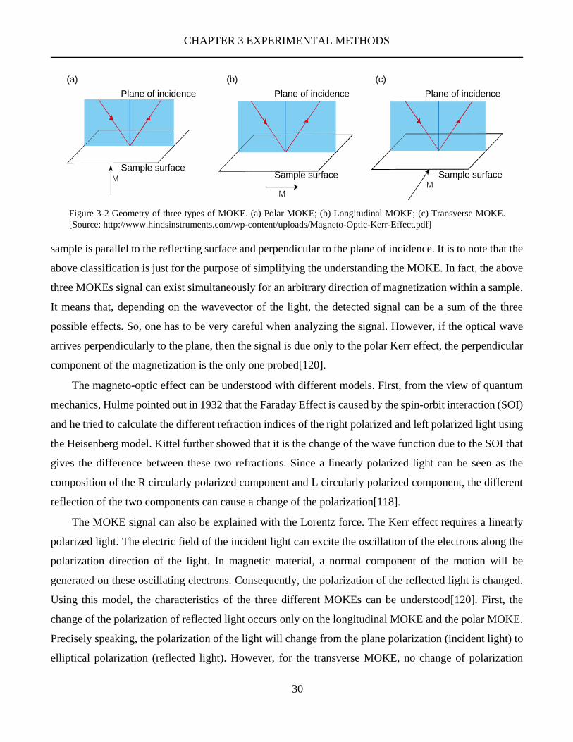
MOKE can be divided into three types, depending on the magnetization direction of the reflecting
sample with respect to the incident plane and the reflecting surface, as shown in Figure 3-2[119]. For the
polar MOKE, the magnetization of the sample is perpendicular to the reflecting surface, thus parallel to
the plane of incidence; For the longitudinal MOKE, the magnetization of the sample is parallel to the
reflecting surface and parallel to the plane of incidence; For the transverse MOKE, the magnetization of
Figure 3-1 Experimental set-up used by John Kerr with which the Kerr effect was discovered.
This sketch was reproduced by P. Weinberger according to the description of John Kerr in his
publication [Philos. Mag. Lett. 2008, 88, 897–907].
CHAPTER 3 EXPERIMENTAL METHODS
30
sample is parallel to the reflecting surface and perpendicular to the plane of incidence. It is to note that the
above classification is just for the purpose of simplifying the understanding the MOKE. In fact, the above
three MOKEs signal can exist simultaneously for an arbitrary direction of magnetization within a sample.
It means that, depending on the wavevector of the light, the detected signal can be a sum of the three
possible effects. So, one has to be very careful when analyzing the signal. However, if the optical wave
arrives perpendicularly to the plane, then the signal is due only to the polar Kerr effect, the perpendicular
component of the magnetization is the only one probed[120].
The magneto-optic effect can be understood with different models. First, from the view of quantum
mechanics, Hulme pointed out in 1932 that the Faraday Effect is caused by the spin-orbit interaction (SOI)
and he tried to calculate the different refraction indices of the right polarized and left polarized light using
the Heisenberg model. Kittel further showed that it is the change of the wave function due to the SOI that
gives the difference between these two refractions. Since a linearly polarized light can be seen as the
composition of the R circularly polarized component and L circularly polarized component, the different
reflection of the two components can cause a change of the polarization[118].
The MOKE signal can also be explained with the Lorentz force. The Kerr effect requires a linearly
polarized light. The electric field of the incident light can excite the oscillation of the electrons along the
polarization direction of the light. In magnetic material, a normal component of the motion will be
generated on these oscillating electrons. Consequently, the polarization of the reflected light is changed.
Using this model, the characteristics of the three different MOKEs can be understood[120]. First, the
change of the polarization of reflected light occurs only on the longitudinal MOKE and the polar MOKE.
Precisely speaking, the polarization of the light will change from the plane polarization (incident light) to
elliptical polarization (reflected light). However, for the transverse MOKE, no change of polarization
M
Sample surface
Plane of incidence
Sample surface
Plane of incidence
M
Sample surface
Plane of incidence
M
(a) (b) (c)
Figure 3-2 Geometry of three types of MOKE. (a) Polar MOKE; (b) Longitudinal MOKE; (c) Transverse MOKE.
[Source: http://www.hindsinstruments.com/wp-content/uploads/Magneto-Optic-Kerr-Effect.pdf]
CHAPTER 3 EXPERIMENTAL METHODS
31
occurs. Instead, a change of the intensity of the light (Kerr reflectivity) occurs. Second, as the incident
angle tends to zero, the longitudinal MOKE will diminish. However, the polar MOKE maintains. As a
consequence, a microscope with perpendicular incident light is sensitive only to the polar Kerr effect. In
other words, it probes only the perpendicular component of the magnetization. As it is the only component
we are interested in the present work, it is perfectly suitable for our purpose. In addition, if the incident
light is normal to the surface of the sample, the Kerr rotation is not affected by the polarization of the
incident light. So, theoretically, the polarization direction of the incident light of a polar MOKE
microscope does not matter.
The Kerr effect changes the linear polarized incident light into a slightly elliptical polarized light,
with a main axis whose direction has rotated as compared to the incident polarization direction. Both the
Kerr rotation and the ellipticity of the reflected light can be used to characterize the magnetic state of the
sample. Analysis based on the dielectric properties of the medium and using the Maxwell boundary
conditions at the interface can give an expression of the Kerr rotation 𝜙′and the ellipticity 𝜙′′. Both 𝜙′and
𝜙′′ are proportional to the magnetization of the material [118].
In general, a polarizer can be implemented before the photodetector to extract the Kerr rotation (this
polarizer is conventionally called analyzer). Supposing that the intensity of the incident light is I = |𝐸𝑝|2,
with Ep the electric field vector of the incident light in the direction of the polarizer. After reflected by a
magnetic material, an orthogonal component ES appears. EP can be filtered out by setting the analyzer in
the crosswise direction with respect to the polarizer (i.e. extinction) before acquiring the signal. Usually,
to get the rotation , the analyzer is a little deviate from the extinction with a small angle δ. Assuming
δ>>𝜙′>>𝜙′′, the intensity of light passed the analyzer is[118],
I ≈ |𝐸𝑃|2|𝛿 + 𝜙′ + 𝜙′′|2 ≈ 𝐼0 (1 +
2𝜙′
𝛿) (3-1)
with 𝐼0 = |𝐸𝑃|2𝛿2, being the intensity of reflected light in the case without Kerr rotation.
The Kerr intensity is defined as the difference in the intensity for a sample magnetized in opposite
directions and normalized by the total polarized light intensity[121],
Δ𝐼
𝐼≈
4𝜙′
𝛿−𝜙′ (3-2)
The above formula is valid only for δ > 𝜙′. One can find that δ should be set to an appropriate value
according the Kerr rotation to maximize the Kerr intensity.

CHAPTER 3 EXPERIMENTAL METHODS
32
Typical optical circuits of Kerr microscopes
MOKE can be applied for two purposes. One is to measure the magnetization evolution of the sample
when scanning the applied field, i.e., measuring the hysteresis loop. Another purpose is to image the
magnetic state of the sample, i.e., the Kerr microscopy.
Figure 3-4 shows the layout of a polar Kerr microscope. For the Kerr microscopy, an objective is
required before the sample. For a polar Kerr microscope, the light is usually incident from the normal
direction of the surface of the sample. Both the incident light and the reflected light pass the objective and
the two beams of light are separated by a splitter. First, the incident light is converged into a very narrow
beam by a lens and becomes polarized after passing a polarizer. Then, the incident light beam is sent into
the objective after the reflection by the light splitter. The incident light beam is transmitted through the
objective and illuminates the field of vision on the sample. After reflected by the sample, part of the light
returns to the objective and partially passed the splitter in the straight direction. This part of the light beam
Figure 3-3 A sketch to describe the Kerr rotation of the reflected light and the polarization direction of the analyzer.

CHAPTER 3 EXPERIMENTAL METHODS
33
is captured by the camera after a filtering by the analyzer. In this way, the optical image of the tested
structure is acquired and Kerr rotation caused by the ferromagnetic material presents in the form of a
contrast of the intensity of the image.
Some key technique points:
The source of the light: a stable light source is strongly desired. After acquiring a series of Kerr
images, a differential operation is required, i.e., subtracting the Kerr image by another one as a reference
to maximize the signal to noise ratio, as shown in Figure 3-5. A stable light illumination can ensure a
consistent intensity for all images. In addition, a light source with a large output power is preferred. Since
the intensity of the light after the filtering by the polarizer and the analyzer has been significantly reduced,
a powerful source ensures a meaningful signal much higher than the parasitic light coming from non
controlled reflexions or light leak from the outside of the setup. In addition, a larger light intensity
promises a shorter exposure time when acquiring a Kerr image, which is important to acquire some
dynamics of the DW. It is very important that all the light arriving on the CCD is coming from the
reflection on the sample, which is the interesting one. So, one must get rid of parasitic light such as leak
Figure 3-4 A typical configuration of the polar Kerr microscope designed by Mr. Nicolas VERNIER.
Light
source
convex lens Polarizer
Analyzer
light
splitter
Objective
Camera
Sample
holder
Magnetic coil
Sample

CHAPTER 3 EXPERIMENTAL METHODS
34
from the lightning of the room or reflections of the beam on some of the setup elements. The Kerr
microscope used in this thesis was completely covered by a double shade cloth to avoid the parasitical
light from the outside. The light beam from the LED is confined in a tube.
The polarizer and analyzer: As the Kerr rotation is very small (at best a few tenths of degrees), very
good polarizer and analyzer are required. An extinction ratio of at least 10-4 is needed, with a very well
defined direction of polarization on the whole area of both polarizers.
The objective: the area of the field of vision and the resolution of the Kerr microscope is largely
determined by the objective implemented. Generally, an objective with a smaller magnification gives a
larger field of vision but a weaker resolution while an objective with a larger magnification gives a better
resolution but the field of vision is reduced. Users can choose a suitable objective according to their
application requirements. The objective should be polarization compatible. In addition, an objective with
long working distance is required so that a large operation space for other configurations between the
objective and the sample is possible. For example, if we want to insert a mini magnetic coil of 2 mm thick,
a working distance of about 4 mm is required considering the space between the sample, the coil, and the
objective.
Like the traditional optical microscopy, the resolution of Kerr microscopes is also constricted by the
problem of the light diffraction. The resolution of a microscope can be described by the Rayleigh criterion
[122–125]:
𝛿𝑑 ≈0.61𝜆
𝑛𝑎 (3-3)
Figure 3-5 (a) Raw Kerr image of an infinite CoFeB magnetic film with saturated magnetization. (b) Kerr image of the
film with a DW. The field of vision of (a) and (b) remains the same. (c) After subtracting (b) by (a), the background
noise, such as the black spot caused by the dust in the sample or in the optical elements, was removed and a net image
with a clear Kerr contrast was obtained.

CHAPTER 3 EXPERIMENTAL METHODS
35
Where 𝛿𝑑 is the minimum distance between two points so that they can be distinguished, λ is the
wave length of the light and na is the numerical aperture of the objective lens. From Rayleigh criterion,
one can hope an ultimate resolution of around 400nm with an optical microscope. With the best lens we
had (Olympus x100, na=0.80, which is not far from the maximum possible) and blue light of wavelength
480nm (fortunately for us, our samples had a good Kerr rotation in the blue), we had a resolution of 370nm.
It was enough to view domains on nanowires as narrow as 200nm.
Camera: since the Kerr signal is finally presented in the form of the contrast of the intensity of light,
a monochrome camera is sufficient for the image acquisition. Considering today’s technology level,
compared with the cameral with the CMOS photosensor, a CCD camera is better in terms of the signal to
noise ratio for the acquisition of Kerr image. In addition, a camera with a cooling plant is preferred to
reduce the noise caused by the heating of the camera.
Configurations of the Kerr microscope for these studies
In this thesis, the sample studied are all with PMA. Correspondingly, a polar Kerr microscope is used.
The layout of the Kerr image is shown in Figure 3-4. This microscope is designed and implemented by
Mr. Nicolas VERNIER. A blue-LED is used as the light source. With an objective of magnification of
100× and the numerical aperture of 0.8, produced by Olympus, the microscopy is able to detect the
magnetic reversal of the 400-nm-large square (see Figure 3-6 (a)) and the DW motion in the 200nm wide
(c)
(a) (b)
Figure 3-6 Examples of Kerr images (after subtracting the background, as explained in Figure 3-5) obtained with our
Kerr microscope. (a) The magnetic reversal of a 400-nm-large square array. (b) The DW motion in a 200-nm-wide wire;
(c) the DW motion in a 1.5-μm-wide wire.

CHAPTER 3 EXPERIMENTAL METHODS
36
nanowires (see Figure 3-6(b)). On the other hand, with an objective of magnification of 4×, the field of
vision can be as large as 1 mm.
Configurations of magnetic coils
To study the field-induced DW motion in nanostructures, three problems have to be solved. First, the
DW nucleation: although the DW nucleation in the magnetic nanowire can be achieved with the Oersted
field produced by a large current pulse through a transverse metal wire, as shown in Figure 3-7 (a), but,
the nanostructure is very easy to be destroyed by the Joule heating in this operation, as shown in Figure
3-7 (b), and this method should be avoided.
Therefore, our strategy is to nucleate a DW by a large and short field pulse. It requires a very large
field magnitude due to the lack of the nucleation point in the nanostructure, e.g., larger than 100 mT for
our sample. Moreover, the field pulse width should be short enough, with a small rising edge and falling
edge, so that the structure cannot be reversed completely because of the propagation occuring during the
pulse. Second, to measure the DW motion velocity in the nanowire, the field pulse should be short enough
so that the propagation distance of the DW is smaller than the length of the wire. For example, the velocity
of the field-induced DW motion in the precessional flow regime is about 5 m/s in the CoFeB nanowire
studied here. With an objective of 100×, the field of vision is about 50 μm. Accordingly, the length of the
magnetic nanowire is usually designed to be less than 50 μm. If we want to observe this motion, the width
of the field pulse applied should be less than 10 μs in order that the DW has not reached the end of the
wire and the propagation length can be measured. Third, the rise time should be much shorter than the
width of the pulse so that the magnetic field can be considered as constant in this duration. All these
requirements demand an intentional design of the magnetic coils.
(a) (b)
Figure 3-7 (a) Schematic diagram of the DW nucleation with Oersted field. A strong current pulse is applied on
the transverse nonmagnetic metal wire and an Oersted field can be produced, resulting the DW nucleation. (b) A
structure destroyed by the Joule heating of the current pulse.

CHAPTER 3 EXPERIMENTAL METHODS
37
As known to all, to reduce the rise time, the number of turns of the coil should be reduced since the
inductance of the coil increases as the turns of the coil increase. However, to obtain a larger field
magnitude, more turns are required. We have to make a tradeoff. Other factors must also be considered,
for example, the Joule heating due to the current passing the coil, which is related to the diameter of the
varnished wire used; the small inductance required and the space of operation, which both limit the size
of the coil; the homogeneity of the field produced in the field of vision observed. To obtain a fast response
and to avoid the remanent field, a magnetic core cannot be used. Parameters which we can play include
the structure, the diameter, the length of the coil, the varnished wire used to fabricate the coil and the
electric configuration for the power supply. In the following, we discuss the design of the coil in a
quantitative manner.
Design of magnetic coils
Design
Supposing a single turn closed coil with a radius R
and that the principal axis is in the z-direction, as shown
in Figure 3-8. When a current I flows in the circuit, the
magnetic field produced in any point P(x,y,z) can be
calculated with the Biot-Savart law. For simplification,
we suppose that the projection of P in the x-y plane is in
the x-axis. In this case, the in-plane component of the
field produced at the position P is parallel to the x-axis,
i.e., By=0. According to the calculation of [126], the
perpendicular component and the in-plane component of
the field produced in a point P(x,0,z) can be expressed as,
𝐵𝑍 =𝜇0𝐼𝑅
4𝜋∫
(𝑅−𝑥 cos𝜃)𝑑𝜃
[𝑥2+𝑧2+𝑅2−2𝑅𝑥 cos𝜃]3/2
2𝜋
0 (3-4)
𝐵𝑥 =𝜇0𝐼𝑅
4𝜋∫
𝑧 cos𝜃𝑑𝜃
[𝑥2+𝑧2+𝑅2−2𝑅𝑥 cos𝜃]3/2
2𝜋
0 (3-5)
The out-of-plane magnetic field created in the center of the loop (x=y=0) is,
𝐵0 =𝜇0𝐼
2𝑅 (3-6)
If z≠0 (which is the case for the sample), this value can be corrected by:
Figure 3-8 Sketch of a coil with single turn closed
circuit.
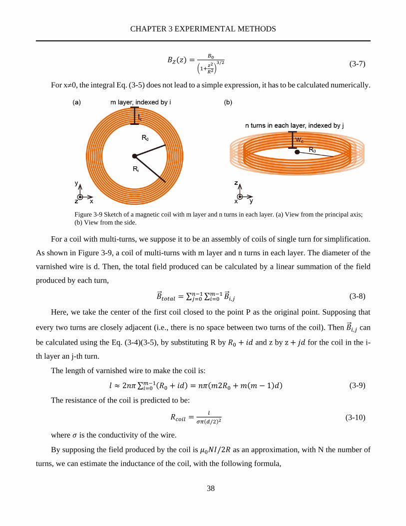
CHAPTER 3 EXPERIMENTAL METHODS
38
𝐵𝑍(𝑧) =
𝐵0
(1+𝑧2
𝑅2)3/2 (3-7)
For x0, the integral Eq. (3-5) does not lead to a simple expression, it has to be calculated numerically.
For a coil with multi-turns, we suppose it to be an assembly of coils of single turn for simplification.
As shown in Figure 3-9, a coil of multi-turns with m layer and n turns in each layer. The diameter of the
varnished wire is d. Then, the total field produced can be calculated by a linear summation of the field
produced by each turn,
�⃗� 𝑡𝑜𝑡𝑎𝑙 = ∑ ∑ �⃗� 𝑖,𝑗𝑚−1𝑖=0
𝑛−1𝑗=0 (3-8)
Here, we take the center of the first coil closed to the point P as the original point. Supposing that
every two turns are closely adjacent (i.e., there is no space between two turns of the coil). Then �⃗� 𝑖,𝑗 can
be calculated using the Eq. (3-4)(3-5), by substituting R by 𝑅0 + 𝑖𝑑 and z by z + 𝑗𝑑 for the coil in the i-
th layer an j-th turn.
The length of varnished wire to make the coil is:
𝑙 ≈ 2𝑛𝜋 ∑ (𝑅0 + 𝑖𝑑)𝑚−1𝑖=0 = 𝑛𝜋(𝑚2𝑅0 + 𝑚(𝑚 − 1)𝑑) (3-9)
The resistance of the coil is predicted to be:
𝑅𝑐𝑜𝑖𝑙 =𝑙
𝜎𝜋(𝑑/2)2 (3-10)
where 𝜎 is the conductivity of the wire.
By supposing the field produced by the coil is 𝜇0𝑁𝐼/2𝑅 as an approximation, with N the number of
turns, we can estimate the inductance of the coil, with the following formula,
Figure 3-9 Sketch of a magnetic coil with m layer and n turns in each layer. (a) View from the principal axis;
(b) View from the side.

CHAPTER 3 EXPERIMENTAL METHODS
39
𝐿 = 𝜇0𝜋𝑁2𝑅/2 (3-11)
where N is the total number of turns, N=m×n
here. S is the cross-section area of the coil, we can
take S = π𝑅2, where R is the radius of the coil. Here,
we may take the average radius �̅� as an
approximation. wc is the length of the solenoid, here,
we take the width of the coil as an approximation, as
indicated in Figure 3-9.
If the overall resistance of the power supply circuit
(including the inner resistance of the power supply) is Rcirc, the rise time can be deduced from the
properties of an LR circuit. When applying a heavy side voltage, the current passing the coil is:
𝐼(𝑡) = 𝐼0 (1 − 𝑒−𝑡
𝜏) (3-12)
where I0 is the saturation current, and τ the characteristic rise time,
𝜏 =𝐿
𝑅𝑐𝑜𝑖𝑙+𝑅𝑐𝑖𝑟𝑐 (3-13)
The power transferred to the Joule heating in the coil can be calculated as,
𝑃 = 𝐼2𝑅𝑐𝑜𝑖𝑙 (3-14)
This equation can be used to evaluate the required output power of the adapted current supply system.
Moreover, the temperature rise of the coil due to Joule heating can be roughly estimated with this equation.
Supposing a coil without effective cooling configuration (e.g. cooling fin or water cooling system) and all
the Joule heating is contributed to the temperature rise of the coil,
𝑃∆𝑡 = 𝐶𝑐𝑜𝑖𝑙𝑚𝑐𝑜𝑖𝑙∆𝑇 (3-15)
Where Δt is the width of a pulse, 𝐶𝑐𝑜𝑖𝑙 is the specific heat capacity of the coil (0.39×10³J/(kg·℃) for
Cu), ΔT is the temperature rise after the pulse, and 𝑚𝑐𝑜𝑖𝑙 is the mass of the coil, which can be
approximately evaluated with the expression 𝑚𝑐𝑜𝑖𝑙 =1
2𝜋2𝑅𝑑2𝑁𝜌𝑉, with 𝜌𝑉 the volume density of the coil
(8.9×10³kg/m3 for Cu).
Considering Eq. (3-4), (3-5) & (3-8), three ways can help to obtain a high magnetic field: increasing
the current flowing in the coil, reducing the size of the coil and increasing the number of turns of wires.
The increase of the current is limited by the ability of the power supply and the heat dissipation efficiency
Figure 3-10 A simple sketch describing the circuit with a
coil.

CHAPTER 3 EXPERIMENTAL METHODS
40
of the coil. In addition, increasing the section of the copper wire is another method to reduce the Joule
heating. However, the size of the coil should be considered when determining the thickness of the wire.
Although increasing the number of turns is helpful to elevate the magnitude of the field, one has to
be careful because the increase of inductance goes faster. Indeed, B increases as N but L increases as N2.
Then, N-value too high would damage the rise time, as described in Eq. (3-11).
At last, reducing the radius of the coil favors both the elevation of the magnitude of the field and a
faster response speed of the coil. However, the homogeneity of the field near the center axis should be
considered. An inhomogeneity of produced field can cause the difficulty of calibration of the coil and can
also result in a field gradient in the field of vision. In addition, the magnitude of the field decreases with
R for a given distance between the coil and sample, with a factor 1/(1+z²/R²)3/2, as described in Eq.(3-7).
We have numerically calculated the distribution of the field produced by a single turn coil based on the
Eq. (3-4) & (3-5). The normalized field vs. the normalized coordinate of the point of view is plotted, as
shown in Figure 3-11. We can see that the order of the field and the homogeneity area depend on the
relative distance of the point of view to the coil with respect to the radius of the coil. A distance about R/2
from the point of view to the coil is optimal to get a satisfying magnitude and homogeneity of the field,
with R the radius of the coil.
(b) (a)
-1 -0.8 -0.6 -0.4 -0.2 0 0.2 0.4 0.6 0.8 1-0.5
-0.3
-0.1
0.1
0.3
0.5
r/R
BIN
P/B
0
z/R=1/4
z/R=1/2
z/R=3/4
z/R=1
-1 -0.8 -0.6 -0.4 -0.2 0 0.2 0.4 0.6 0.8 10
0.2
0.4
0.6
0.8
1
1.2
1.4
r/R
BZ/B
0
z/R=0
z/R=1/4
z/R=1/2
z/R=3/4
z/R=1
Figure 3-11 Magnetic field produced by a coil of single turn with a radius R. The vertical axis represents (a) the
perpendicular component (i.e. in z-direction) and (b) the in-plane component of the field. Each line denotes the
distribution of the field in a plane which is parallel to the surface of the coil and with a distance z to the coil. The field is
normalized by the field B0=μ0I/(2R), equaling to the field produced in the center of the coil. The abscissa axis denotes
the radical coordinates normalized by R. Note that these relationships are always valid, irrespective of the dimension of
R and I.

CHAPTER 3 EXPERIMENTAL METHODS
41
In the practical implementation, the coil cannot be very close to the sample because of several
constraints, such as the thickness of the sample (~0.5mm), the thickness of the sample holder (~1.5mm)
and the interspace between the coil and sample holder (~0.3mm, this interspace is necessary in order that
the sample is removable for the focusing and to change the observed structure). We were not able to
implement the coil between the objective and the sample because of the short work distance of the 100×
objective (3.4 mm). Moreover, the further electric test requires a wire connection before the sample. At
last, the coil is placed in the back of the sample holder, with a distance about 2.3 mm to the focus plane.
Considering this distance, a coil with a radius of 4.5
mm is optimal for our configuration.
As can be seen from Figure 3-11, the field viewed
by the sample falls rapidly as the distance from the
sample to the coil increases. Therefore, the width of
the coil wc should not be too large to make sure that
fields produced by all the turns are effective in the
tested area.
At last, a series of coils with an average diameter
of 6 to 8 mm, and a thickness wc of 1mm were
fabricated. Here, wc is the thickness of the coil, as
N° of coil Nb of
turns
Diameter
(mm)
Resistance
(Ω)
Rise time when
connected in series
with 50 ohm (µs)
Inductance
(µH)
Field
(mT/A
)
Distance from
coil to sample
(mm)
10 100 6.5-11 8.9 1.68 151 8.95 2.3
12 120 6-10 10 1.92 192 10.2 2.3
13 60 6-8 4.9 0.32 47 4.65 2.3
14 40 6-7.8 3.2 0.18 28 3.49 2.3
15 20 6-7 1.9 0.045 13 1.55 2.3
16_int 120 6-10.5 10.5 2.16 175 9.4 2.3
16_ext 20 10.5-12 2.6 0.228 19 1.63
17_int 120 5-8 9.4 1.72 164 8.9 2.5
17_ext 20 19 4.3 0.26 30 0.92
Helmholtz
coil 60/side 116-132
1.1 (two in
series) 20 1900 0.91 In center
Table 3-1 Parameters of the coil fabricated. The inductance is measured with a handheld multimeter, the uncertainty may be
very large.
3 cm
Figure 3-12 An example of the mounted coil.
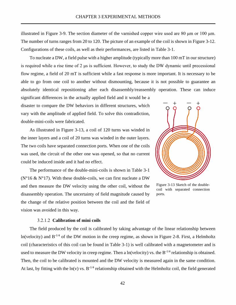
CHAPTER 3 EXPERIMENTAL METHODS
42
illustrated in Figure 3-9. The section diameter of the varnished copper wire used are 80 μm or 100 μm.
The number of turns ranges from 20 to 120. The picture of an example of the coil is shown in Figure 3-12.
Configurations of these coils, as well as their performances, are listed in Table 3-1.
To nucleate a DW, a field pulse with a higher amplitude (typically more than 100 mT in our structure)
is required while a rise time of 2 μs is sufficient. However, to study the DW dynamic until precessional
flow regime, a field of 20 mT is sufficient while a fast response is more important. It is necessary to be
able to go from one coil to another without dismounting, because it is not possible to guarantee an
absolutely identical repositioning after each disassembly/reassembly operation. These can induce
significant differences in the actually applied field and it would be a
disaster to compare the DW behaviors in different structures, which
vary with the amplitude of applied field. To solve this contradiction,
double-mini-coils were fabricated.
As illustrated in Figure 3-13, a coil of 120 turns was winded in
the inner layers and a coil of 20 turns was winded in the outer layers.
The two coils have separated connection ports. When one of the coils
was used, the circuit of the other one was opened, so that no current
could be induced inside and it had no effect.
The performance of the double-mini-coils is shown in Table 3-1
(N°16 & N°17). With these double-coils, we can first nucleate a DW
and then measure the DW velocity using the other coil, without the
disassembly operation. The uncertainty of field magnitude caused by
the change of the relative position between the coil and the field of
vision was avoided in this way.
Calibration of mini coils
The field produced by the coil is calibrated by taking advantage of the linear relationship between
ln(velocity) and B-1/4 of the DW motion in the creep regime, as shown in Figure 2-8. First, a Helmholtz
coil (characteristics of this coil can be found in Table 3-1) is well calibrated with a magnetometer and is
used to measure the DW velocity in creep regime. Then a ln(velocity) vs. the B-1/4 relationship is obtained.
Then, the coil to be calibrated is mounted and the DW velocity is measured again in the same condition.
At last, by fitting with the ln(v) vs. B-1/4 relationship obtained with the Helmholtz coil, the field generated
Figure 3-13 Sketch of the double-
coil with separated connection
ports.
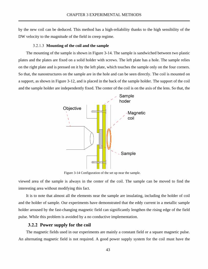
CHAPTER 3 EXPERIMENTAL METHODS
43
by the new coil can be deduced. This method has a high-reliability thanks to the high sensibility of the
DW velocity to the magnitude of the field in creep regime.
Mounting of the coil and the sample
The mounting of the sample is shown in Figure 3-14. The sample is sandwiched between two plastic
plates and the plates are fixed on a solid holder with screws. The left plate has a hole. The sample relies
on the right plate and is pressed on it by the left plate, which touches the sample only on the four corners.
So that, the nanostructures on the sample are in the hole and can be seen directly. The coil is mounted on
a support, as shown in Figure 3-12, and is placed in the back of the sample holder. The support of the coil
and the sample holder are independently fixed. The center of the coil is on the axis of the lens. So that, the
viewed area of the sample is always in the center of the coil. The sample can be moved to find the
interesting area without modifying this fact.
It is to note that almost all the elements near the sample are insulating, including the holder of coil
and the holder of sample. Our experiments have demonstrated that the eddy current in a metallic sample
holder aroused by the fast-changing magnetic field can significantly lengthen the rising edge of the field
pulse. While this problem is avoided by a no conductive implementation.
Power supply for the coil
The magnetic fields used in our experiments are mainly a constant field or a square magnetic pulse.
An alternating magnetic field is not required. A good power supply system for the coil must have the
Figure 3-14 Configuration of the set up near the sample.

CHAPTER 3 EXPERIMENTAL METHODS
44
following characteristics: first, the output power and the supplied current should be large enough during
the period of the field pulse. Second, a stable current output is required to obtain a stable field, especially
at the beginning and at the end of the field pulse. An overshot is catastrophic for the measurement of the
DW velocity. Third, the rise time of the power supply should be fast, at least faster than the rise time of
the coil.
Figure 3-15 shows the circuit diagram of a power supply system which allows us to obtain a field
pulse with width from 100 μs to the order of seconds. The ON-OFF is controlled by a transistor whose
gate voltage is governed by the signal from a function generator. A shunt resistor of 0.2 Ω is connected
into the circuit so that the current passed the circuit can be completely supervised via an oscilloscope. A
battery or a voltage supply can be used as the power source. The rise time of the voltage supply we used
is about 100 μs (i.e. when the transistor is set to ON, the output voltage reaches a stable state after 100 μs).
The response speed of battery is very fast, much faster than the coil. A proper field pulse with a width of
several hundred microseconds can be obtained with this system equipped with the mini coil we fabricated.
If a battery is used as the power supply, the amplitude of the field pulse can be adjusted via a rheostat. A
current pulse as high as 3A can be applied with this system. The key constraints that limit the amplitude
the current flowing in the coil are the current of the transistor and the coil itself because of the Joule
heating if the pulse duration is relatively long. Two examples of the field pulse produced with this power
Figure 3-15 A power supply circuit for the coil to produce a field pulse ≥ 50 μm.
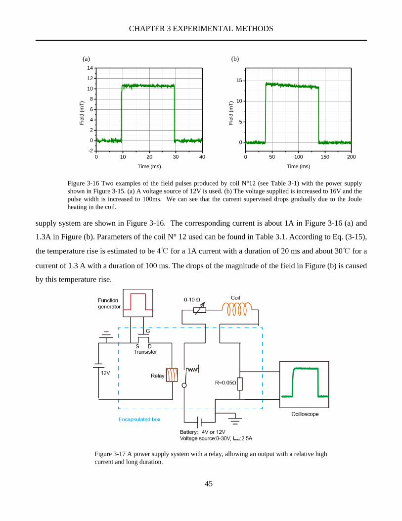
CHAPTER 3 EXPERIMENTAL METHODS
45
supply system are shown in Figure 3-16. The corresponding current is about 1A in Figure 3-16 (a) and
1.3A in Figure (b). Parameters of the coil N° 12 used can be found in Table 3.1. According to Eq. (3-15),
the temperature rise is estimated to be 4℃ for a 1A current with a duration of 20 ms and about 30℃ for a
current of 1.3 A with a duration of 100 ms. The drops of the magnitude of the field in Figure (b) is caused
by this temperature rise.
0 10 20 30 40
-2
0
2
4
6
8
10
12
14
Fie
ld (
mT
)
Time (ms)
0 50 100 150 200
0
5
10
15
Fie
ld (
mT
)
Time (ms)
(a) (b)
Figure 3-16 Two examples of the field pulses produced by coil N°12 (see Table 3-1) with the power supply
shown in Figure 3-15. (a) A voltage source of 12V is used. (b) The voltage supplied is increased to 16V and the
pulse width is increased to 100ms. We can see that the current supervised drops gradually due to the Joule
heating in the coil.
Figure 3-17 A power supply system with a relay, allowing an output with a relative high
current and long duration.

CHAPTER 3 EXPERIMENTAL METHODS
46
To overcome the constraint of current density by the transistor, a more robust power supply system
was created. As shown in Figure 3-17, the OFF-ON of the power supply circuit is governed by a relay.
The circuit controlling the OFF-ON of the relay is governed by a transistor and a function generator. This
system allows a relatively large current density (20A, precisely) and longer width of the pulse. However,
the relay introduced a delay of the field pulse about 15 ms after the command from the function generator.
We have used another implementation that can produce a field pulse with both large amplitude and
short rise time. As can be seen from Eq. (3-13), to decrease the rise time of the field pulse, a large resistance
can be connected in series with the coil. Eq. (3-4) shows that to obtain a high field, a large current is
necessary, thus requiring a very high voltage supply after the introduction of the large resistance. An
ordinary voltage/current source cannot supply such a high power and with a fast response speed. A power
supply based on the discharge of condenser bank can solve this issue[127,128]. As shown in Figure 3-18,
a current supply of this type is implemented. The condenser bank is charged with a high-voltage supply.
Once the transistor is ON, a high current will be generated by the discharge of the condensers.
Figure 3-19 shows two examples of the field pulses generated with this system. With a coil of 120
turns and 8 mm large, the amplitude of the field pulse has reached 130 mT. This field is sufficient to
nucleate a DW in the microstructure. The rise time (falling time) is less than 2 μs. Thanks to the short
falling edge, the nucleated DW still remains in the structure after the pulse. Using a coil of 20 turns, an
even shorter rising edge is obtained. The field can reach the plateau within 500 ns. This field allows us to
measure the DW velocity in the nanostructure with very high precision. An amplitude of 23 mT is
sufficient to study the DW behavior in processional flow regime in soft material such as the CoFeB.
Figure 3-18 A power supply system based on the discharge of a condenser bank.

CHAPTER 3 EXPERIMENTAL METHODS
47
However, compared with the former two power supply system, the disadvantage of this supply is the
relatively short rated pulse duration of only 10 μs.
With the above three power supply systems and coils with various configurations, different kind of
field pulses can be generated, allowing us to study the DW dynamics in different regimes.
Configurations for electrical tests
It is interesting to study the DW dynamics when the magnetic field and the electric current are applied
simultaneously. We have developed a system in which a clear magnetic field pulse and a current pulse are
compatible.
As discussed above, in order to ensure the magnitude of the pulse viewed by the sample, the distance
between the sample and the coil should be as short as 2 mm when a mini coil is used. Moreover, the
sample holder should be insulating. An ordinary chip carrier is not a good choice. In this case, we have
printed several conductive strips in the sample holder (the plastic plate in the back of the sample, as shown
in Figure 3-14). In these experiments, the implementation in Figure 3-14 is a little changed: the sample is
stick into the right plastic plate with silver lacquer and the plate in front of the sample is removed. Then,
the nanostructure was connected into the electric test circuit after wire bonding between the electrodes
and these conductive strips. An example of the configuration is shown in Figure 3-20.
0 5 10 15 20
0
50
100
150
Fie
ld (
mT
)
Time (μs)
Field
0 2 4 6 8
-5
0
5
10
15
20
25
30
Fie
ld (
mT
)
Time (μs)
(a) (b)
Figure 3-19 Two examples of the magnetic field pulse produced with power supply system shown in Figure 3-18.
(a) The coil used is coil N°12 (see Table 3-1), with 120 turns. (b) The coil used is N°16_ext, with 20 turns.

CHAPTER 3 EXPERIMENTAL METHODS
48
Figure 3-21 gives a schematic diagram of the complete configuration of the electrical tests circuit.
The pulse generator can supply a voltage pulse of 20V (high impedance mode). By measuring the voltage
Figure 3-21 Sketch showing the complete configuration for electrical tests.
Figure 3-20 An example of the electrical test configuration: the sample is stick into a plastic
plate with silver lacquer and the electrodes of microstructures are wire bonded with the
copper stripes.
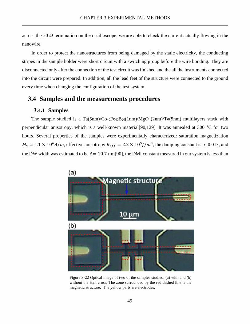
CHAPTER 3 EXPERIMENTAL METHODS
49
across the 50 Ω termination on the oscilloscope, we are able to check the current actually flowing in the
nanowire.
In order to protect the nanostructures from being damaged by the static electricity, the conducting
stripes in the sample holder were short circuit with a switching group before the wire bonding. They are
disconnected only after the connection of the test circuit was finished and the all the instruments connected
into the circuit were prepared. In addition, all the lead feet of the structure were connected to the ground
every time when changing the configuration of the test system.
Samples and the measurements procedures
Samples
The sample studied is a Ta(5nm)/Co40Fe40B20(1nm)/MgO (2nm)/Ta(5nm) multilayers stack with
perpendicular anisotropy, which is a well-known material[90,129]. It was annealed at 300 °C for two
hours. Several properties of the samples were experimentally characterized: saturation magnetization
𝑀𝑆 = 1.1 × 10⁶𝐴/𝑚, effective anisotropy 𝐾𝑒𝑓𝑓 = 2.2 × 10⁵𝐽/𝑚3, the damping constant is α=0.013, and
the DW width was estimated to be ∆= 10.7 nm[90], the DMI constant measured in our system is less than
Figure 3-22 Optical image of two of the samples studied, (a) with and (b)
without the Hall cross. The zone surrounded by the red dashed line is the
magnetic structure. The yellow parts are electrodes.

CHAPTER 3 EXPERIMENTAL METHODS
50
0.01mJ/m2, meaning that its effect on the DW surface energy is negligible[24]. This result is also
confirmed by Brillouin light scattering experiments.
One sample remains unpatterned and studied as a reference. Another sample was patterned by
conventional electron beam lithography and ion beam etching into 50 µm long narrow wires connected
with a 20µ×20µm square (nucleation pad), as shown in Figure 3-22. The size of the magnetic square is 20
μm ×20 μm and the width of the wire in different structures are 200nm, 400nmm 600nm, 1µm and 1.5µm
respectively. In some structures, Hall crosses were patterned, as shown in Figure 3-22 (b). Several golden
electrodes were added on the magnetic structure for the electrical tests.
Nucleation of DW
As stated at the beginning of the section 3.2 , our methods to nucleate a DW in the nanostructure is
applying a large and short magnetic field pulse. First, the magnetic structure is saturated in one direction
by a permanent magnet or by a large field pulse (~ 130 mT). Then, a field pulse in the opposite direction
is applied by a magnetic coil with 120 turns. One typical waveform of the pulse is shown in Figure 3-19
(a). Usually, a magnetic reversal (DW nucleation) first occurs in the nucleation pad owing to its large
surface, which promises a large probability to have a nucleation point. To ensure that the nucleated DW
stay still in the nanostructure after the field pulse, the length of the field pulse should be well controlled.
According to our experiments, a DW can be obtained in most of the structures studied when applying a
field pulse by an exponential field pulse with an amplitude of 130 mT and a pulse width of 4 – 8 μs.
Measurement of the DW velocity
The DW motion velocities in all our experiments were obtained through observing the DW motion
distance by a field pulse. Precisely, before and after applying a field pulse with width Tp, we take two Kerr
images respectively. After comparing these two Kerr images, we can obtain the DW motion distance D
during this pulse. Then, the corresponding DW motion velocity can be calculated as v=D/Tp.
In particular, for the DW velocity measurement in the nanostructure, the width of the field pulse
should be very short. In these experiments, after nucleating a DW with the 120-turns-coil of the double
coils, we pass to the 20-turns-coil without disassembly the coil implantation. A 220 ns rise time of this
coil gives a very good rectangle square waveform field pulse with a width of several microseconds, as
shown in Figure 3-19 (b). In order to improve the accuracy of the measurement, we used the differential
methods. That is to say, first, we measured the DW motion distance D1 by applying a field pulse with a

CHAPTER 3 EXPERIMENTAL METHODS
51
relatively long width t1; then, we measure the DW motion distance D2 after a field pulse width a relatively
short width t2. The DW velocity is calculated as, 𝑣 = (𝐷1 − 𝐷2) (𝑡1 − 𝑡2)⁄ .
At the beginning of the thesis, in order to have a global view of the characteristic of the sample to be
studied, the field-induced DW motion velocity in the infinite film was measured with a large field range,
as shown in Figure 3-23.
Figure 3-23 DW motion velocity in the Ta/CoFeB/MgO infinite film vs. the
applied field.
0 20 40 60 80 100
0
2
4
6
8
DW
velo
city (
m/s
)
Applied field (mT)
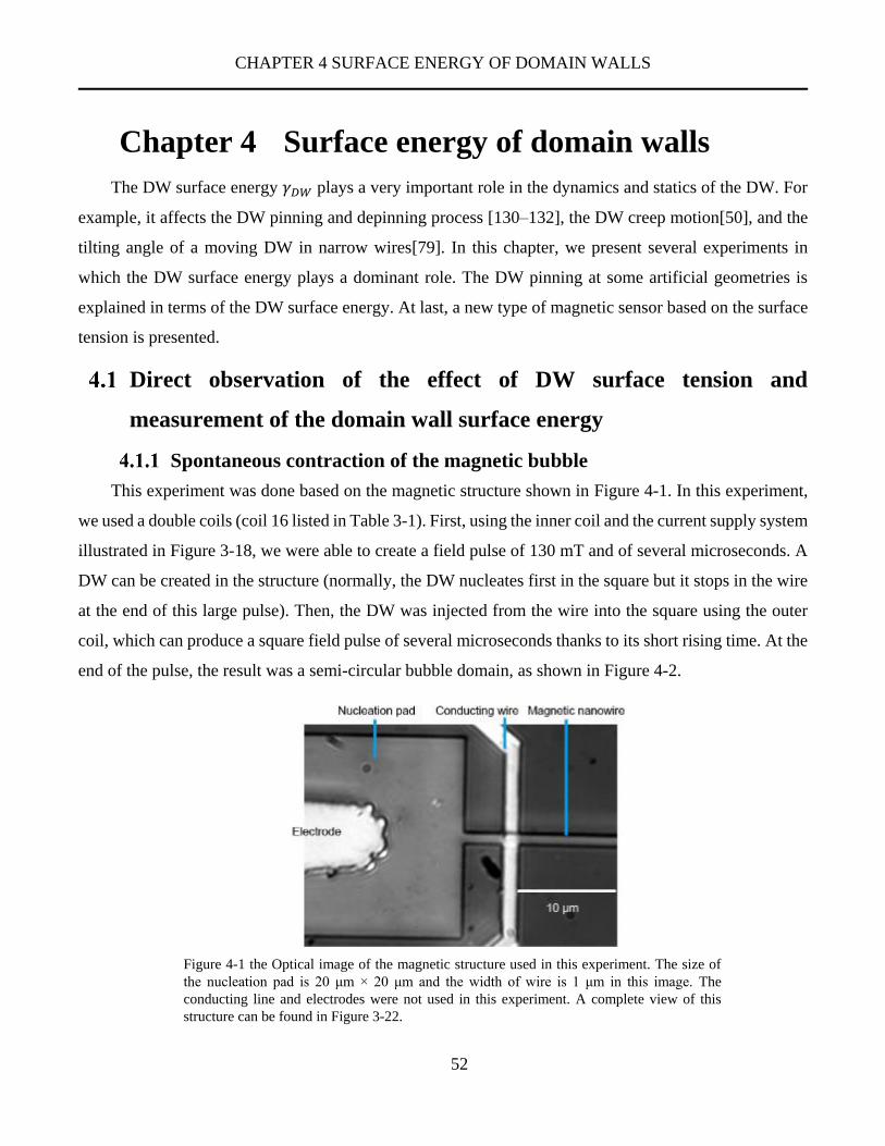
CHAPTER 4 SURFACE ENERGY OF DOMAIN WALLS
52
Chapter 4 Surface energy of domain walls
The DW surface energy 𝛾𝐷𝑊 plays a very important role in the dynamics and statics of the DW. For
example, it affects the DW pinning and depinning process [130–132], the DW creep motion[50], and the
tilting angle of a moving DW in narrow wires[79]. In this chapter, we present several experiments in
which the DW surface energy plays a dominant role. The DW pinning at some artificial geometries is
explained in terms of the DW surface energy. At last, a new type of magnetic sensor based on the surface
tension is presented.
Direct observation of the effect of DW surface tension and
measurement of the domain wall surface energy
Spontaneous contraction of the magnetic bubble
This experiment was done based on the magnetic structure shown in Figure 4-1. In this experiment,
we used a double coils (coil 16 listed in Table 3-1). First, using the inner coil and the current supply system
illustrated in Figure 3-18, we were able to create a field pulse of 130 mT and of several microseconds. A
DW can be created in the structure (normally, the DW nucleates first in the square but it stops in the wire
at the end of this large pulse). Then, the DW was injected from the wire into the square using the outer
coil, which can produce a square field pulse of several microseconds thanks to its short rising time. At the
end of the pulse, the result was a semi-circular bubble domain, as shown in Figure 4-2.
Figure 4-1 the Optical image of the magnetic structure used in this experiment. The size of
the nucleation pad is 20 μm × 20 μm and the width of wire is 1 μm in this image. The
conducting line and electrodes were not used in this experiment. A complete view of this
structure can be found in Figure 3-22.

CHAPTER 4 SURFACE ENERGY OF DOMAIN WALLS
53
Subsequently, although the magnetic field was zero, we found that the bubble could contract
spontaneously until the DW had come back to the entrance of the nucleation pad, i.e., the neck.
Furthermore, the speed of contraction depended on the radius of curvature of the DW circle. The smaller
the radius, the faster was the contraction. As shown in Figure 4-3, when the radius of the bubble is
approximately 9 μm, the DW contraction is observable only after 20 s. However, when the radius of the
DW bubble shrinks to 4 μm, DW returns to the neck after several seconds. After returning to the neck, no
more DW motion could be observed during several minutes; the state is stable.
We checked that there was no remnant parasitic field that could induce such an effect. The sample
holder was made of a non-magnetic material, and a Hall probe was used to check the magnetic field around
the sample. In addition, the experiment was conducted with both directions of the magnetization of the
Figure 4-2 Spontaneous contraction of the semicircular domain bubble in a zero external field.

CHAPTER 4 SURFACE ENERGY OF DOMAIN WALLS
54
bubble and the result was exactly the same, which would not have been the case if there had been a remnant
field.
The Laplace pressure of a bend DW
In physics, the concept of the Laplace pressure is commonly used to explain the surface and interface
phenomena[133,134]. The Laplace pressure indicates the pressure difference between the inside and the
outside of a curved surface or interface.
A DW can be seen as an elastic membrane with energy 𝛾𝐷𝑊 per unit area[135]. For a bend DW, there
is also such a pressure. In a bulk magnetic material, the Laplace pressure of a spherical DW expressed
as[135],
𝑃𝛾 = γ𝐷𝑊 (1
𝑅1+
1
𝑅2)⁄ (4-1)
where R1 and R2 are the principal radii of curvature of the wall at the point considered.
Figure 4-3 3D sketch of the profile of the semicircular magnetic bubble stabilized in the square. The arrows on
the DW show the forces induced by the different pressures on this part. As the pressures are isotropic, the
direction of the local forces point perpendicularly to the surface of DW and changes according to the position
on the DW.
PH_ext
Pdemag
Applied field
m
DW
tM
Pγw

CHAPTER 4 SURFACE ENERGY OF DOMAIN WALLS
55
In a thin film, the curved DW is a cylindrical surface of radius R, as shown in Figure 4-3. Then the
Laplace pressure can be written as[134–136],
𝑃𝛾 = γ𝐷𝑊 𝑅⁄ (4-2)
Where R is the curvature of radius of the DW. (Appendix 1 presents a demonstration of this result).
The Laplace pressure is high enough to induce some movement on the bubble in the creep regime.
Note that it remains a relatively low force; the movement is possible because CoFeB is very soft[40].
Moreover, the bubbles created had a quite small radius (<10 μm), which induces a quite big Laplace
pressure. In agreement with 𝑃𝛾 = 𝛾𝐷𝑊/𝑅, the spontaneous contraction was faster as the radius of the
domain reduced.
Stabilization of the magnetic bubble and estimation of the DW surface
energy
To quantify the Laplace pressure, the external field needed to compensate this pressure and stabilize
domain bubble was measured by the following way: First, a very small static field is applied using the
inner coil of the double-coils. Second, we created a semicircular bubble domain using a large square-
shaped field pulse produced by the outer coil. In the experiments, the initial size of the semicircular domain
bubbles can be controlled through the magnitude and the duration of the field pulse when blowing the DW
into the square. To check whether it is stable or not under the static field, we have waited for 60 s. If no
movement was detected after 60 s (for example, in the case of Figure 4-4 (b), there is a movement), the
state can be considered as stable. Then the static field was increased (or decreased) by step of 20 μT until
a movement is detected. In Figure 4-4(c), critical fields for expansion and for contraction were plotted as
a function of the inverse of the radius of the domain bubble. The equilibrium field is between the two
clouds of critical fields for expansion and for contraction. Its magnitude is quite well defined. As could be
expected, this field had to be applied along the magnetization direction inside the bubble.
It was found that the magnitude of the external field to stabilize the semicircular domain bubble
depended on the size of bubbles. As the radius of the domain bubble is reduced, the stabilization field
increased sharply.
Theoretically, a circular DW is at equilibrium only when the pressure due to the magnetic field
exactly cancels out the excess pressure from the DW tension. The Zeeman pressure given by the external
field Hext is expressed as
𝑃𝐻 = 2𝜇0𝐻𝑒𝑥𝑡𝑀𝑆 (4-3)

CHAPTER 4 SURFACE ENERGY OF DOMAIN WALLS
56
According to Eq. (4-2), the Laplace pressure increases linearly as the inverse of the radius of the DW
bubble. The field required to stabilize the semi-bubble should be inversely proportional to the radius. In
Figure 4-4(c), the stabilizing field appears as the boundary between the expansion points and contraction
points. We can see Figure 4-4(c) that there is a very good agreement between the predicted behavior and
the experimental one, the slope being 𝑘𝑒𝑞𝑢 ≈ 1.2 𝑚𝑇 ∙ 𝜇𝑚.
However, one should be careful because there are two contributions for the magnetic field: the
externally applied field and the demagnetizing field. We have numerically calculated the demagnetizing
field. To obtain this field, we have used the magnetization current[1,137]. Let us remember that the
magnetization is defined as the volume density of magnetic moment �⃗⃗� 𝑚 (see Eq.(2-1)) and each
(a) (b)
(c)
0.0 0.1 0.2 0.30.0
0.2
0.4
0.6
Min field observed for expansion
Max field observed for contraction
Fie
ld (
mT
)
1/Radius (R in μm)
Figure 4-4(a) A semi bubble is stabilized by an external field 𝜇0𝐻𝑒𝑥𝑡 = 0.11 𝑚𝑇 and no DW motion
is observed during 60s; (b) The external field decreases to 𝜇0𝐻𝑒𝑥𝑡 = 0.094 𝑚𝑇 T and the domain
bubble contracts slightly. This image is the difference between two images: the first one was acquired
before decreasing the applied field and the second one was acquired 66s after having decreased the
applied field. The white circular trace shows the DW displacement; (c) Critical field for expansion
and contraction as a function of the inverse of the radius of the semicircular domain bubble. Two
structures associated with 600 nm wide wire were used to get more statistics.

CHAPTER 4 SURFACE ENERGY OF DOMAIN WALLS
57
elementary magnetic moment can be seen as a loop of current of magnetic moment d�⃗⃗� 𝑚 = 𝐼𝑑�⃗⃗� , where I
is the current flowing inside the loop and 𝑑�⃗⃗� is the surface of the loop. For a uniformly magnetized out-
of-plane domain, the magnetization density can be expressed as,
𝑀𝑠𝑧 = 𝐼𝑑𝑆𝑧
𝑑𝑉=
𝐼
𝑡𝑀𝑧 (4-4)
where 𝑧 is the unit vector in the out of plane
direction. Let's note that, looking at picture 4.5, it is
straightforward: the effective current of each
elementary magnetic dipole is cancelled by the
neighboring dipoles, except for the dipoles at the edge
of the domain. For the structure we studied in the
experiments, the demagnetizing field can be deduced
from the electrical circuit shown in Figure 4-6(a).
Using MATLAB, we calculated the demagnetizing
field for a radius from 3 μm to 10 μm. The result is
plotted in Figure 4-6(b). It can be seen that, in this
range, this demagnetizing field can be approximated by
a linear law, of slope 𝑘𝑑𝑒𝑚𝑎𝑔 ≈ 1.24 𝑚𝑇 ∙ 𝜇𝑚.
From the above considerations, equilibrium of the
pressures can be written as follows:
2𝜇0𝐻𝑒𝑥𝑡𝑀𝑆 + 2𝜇0𝐻𝑑𝑒𝑚𝑎𝑔𝑀𝑆 −γ𝐷𝑊
𝑅= 0 (4-5)
Using the linear laws found for 𝜇0𝐻𝑑𝑒𝑚𝑎𝑔 = 𝑘𝑑𝑒𝑚𝑎𝑔 𝑅⁄ and the equilibrium field 𝜇0𝐻𝑒𝑞𝑢 = 𝑘𝑒𝑞𝑢 𝑅⁄ ,
and simplifying by 1/R, the surface energy of DW is given by:
γ𝐷𝑊 = 2𝑀𝑆(𝑘𝑒𝑞𝑢 + 𝑘𝑑𝑒𝑚𝑎𝑔) (4-6)
From Eq. (4-3), we get γ𝐷𝑊 ≈ 5.4 mJ/𝑚2. From[138,139], the exchange stiffness Aex in this type of
material was found to be between 10 and 28 pJ/m. For our sample, the effective anisotropy was measured
as 𝐾𝑒𝑓𝑓 = 2.2 × 10⁵𝐽/𝑚3 [90]. According to the formula γ𝐷𝑊 = 4√𝐴𝑒𝑥𝐾𝑒𝑓𝑓 , it gives γ𝐷𝑊 between 6
and 10 mJ/m2. It can be seen that our value is in good agreement with the previous results. Note that the
formula used here to calculate the surface energy γ applies only for films without DMI. In fact, the DMI
Figure 4-5 Magnetization current of the magnetic
structure (a uniformly magnetized disk in this
sketch)
I=tmMS

CHAPTER 4 SURFACE ENERGY OF DOMAIN WALLS
58
constant measured in our system is less than 0.01mJ/m2, meaning that its effect on the DW surface energy
is negligible[24]. This result is also confirmed by Brillouin light scattering experiments.
Interactions of two magnetic domain bubbles
As suggested before, the behavior of magnetic bubbles induced by the surface energy is similar to
that of soap bubbles. There is a very well-known experiment in which two soap bubbles are connected to
each other, as illustrated in Figure 4-7; the result is not what one might expect intuitively. Instead of
obtaining two bubbles of equal size, the smaller bubble contracts while the bigger one expands due to the
unbalanced Laplace pressure [134,136,140].
Here, we observed the same phenomenon. We simultaneously created two semicircular bubbles with
different sizes in a magnetic square, as shown in Figure 4-8. An external field 𝜇0𝐻𝑒𝑥𝑡 = 0.41𝑚𝑇 was
applied to avoid the collapse of both bubbles. In the beginning, the smaller magnetic bubble was stable
while the larger one expanded slowly. When the two bubbles got close, the bigger bubbles continued to
expand while the smaller one contracted back to the neck, as shown in Figure 4-8.
(b) (a)
0.0 0.1 0.2 0.30.0
0.1
0.2
0.3
0.4
Calculated numerically
Linear fitting result
Dem
agn
etiz
ing
fie
ld (
mT
)
1/Radius (R in μm)
Intercept 0
Slope 1.24 mT·μm
Figure 4-6 (a) Electrical circuit identical to the current created by the magnetization at the edges of structure and along
the DW. Then, using Biot-Savart law, stray field can be calculated; (b) Numerically calculated demagnetizing field at
point P as a function of the inverse of radius of bubble.

CHAPTER 4 SURFACE ENERGY OF DOMAIN WALLS
59
The competition of three pressures governs this process: the Zeeman pressure tends to enlarge the
size of both bubbles; the repulsive pressure between the two bubbles due to dipolar interaction[1] hinders
the merger of the two bubbles; the Laplace pressure tends to reduce the sizes of the bubbles. The strength
Figure 4-8 Size evolution of two semicircular bubbles under applied field 0.41 mT. The bigger bubble
expands and squeezes the smaller one because of the unbalanced Laplace pressure. The movie on this
dynamic process can be download online.
Figure 4-7 Sketch of experiments about the interplay of two soap bubbles.

CHAPTER 4 SURFACE ENERGY OF DOMAIN WALLS
60
of the former two pressures is equal for the two bubbles while the Laplace pressure is higher for the smaller
bubble, as predicted by Eq. (4-1). Finally, the smaller bubble is squeezed by the larger one.
DW pinning and depinning at Hall crosses or at necks
Thanks to the theory of the DW surface energy and the Laplace pressure, it becomes possible to
explain the origin of the DW pinning effects in some geometries, such as the connection of the wire with
the nucleation pad, and the Hall cross.
Indeed, when injecting a DW from the narrow wire into the square, we found that the DW was pinned
at the neck and would not be depinned until the applied field reached a threshold value. As shown in
Figure 4-9(a), the DW was moved by a field pulse. After the pulse, we could see that the DW stopped at
Figure 4-9 (a) DW depinning at the neck: Image n°0 is the raw image of a structure, with a 1μm wide wire. As the
magnetization was saturated before acquiring it, it is used as the reference image to remove the background and get
the Kerr image. Image n°1 shows the initial position of the DW. After a field pulse of 5.8mT and 5 μs, the DW moves
to the neck (image n°2). One more identical pulse could not move it. After increasing the magnitude of pulse to 5.9
mT, the DW is depinned and expands to a semicircular bubble (on image n°3); (b) DW depinning at a Hall cross: the
sequence is similar to sequence (a), n°0 is the raw reference image of a 1 μm wide wire. Between each picture from
n°1 to n°3, a pulse of 5.9 mT and 5 μs is applied. With these pulses, the DW is moved in the wire but is pinned at the
Hall cross. Between n°3 and n°4, a field pulse of 6.0 mT and 5 μs is applied and the DW is depinned.
(a) (b)
CHAPTER 4 SURFACE ENERGY OF DOMAIN WALLS
61
the neck. We tried to send more pulses of the same magnitude, but no more movement occurred; the DW
remained pinned at the neck. To depin the DW, we had to increase the magnitude of the field; the critical
field to achieve the movement is called the depinning field Hdep here. It should be noted that the duration
of field pulse was always 5 μs in these measurements. We repeated this experiment several times for each
sample. The depinning field was almost always the same. For Hall crosses, the behavior is the same
[(Figure 4-9(b)]: pinning, if the magnetic field is below a critical field, and movement above it.
The interesting point is that the depinning field depends on the width of the wire. We have plotted
Hdep in Figure 4-9 (c). It can be seen that there is a linear dependence of Hdep as a function of the inverse
of the width. Furthermore, the dependence is almost same for the Hall cross or for the neck of the pad. Let
us note that when 1/R tends to zero, the depinning field tends to 𝜇0𝐻0 = 3 𝑚𝑇. This is explained by the
velocity law. Below 3mT, for pulses of 5μs, no effective movement is possible. Movement requires a field
larger than a minimum value 𝐻𝑃, which can be estimated at 3 mT[90]. Indeed, even if for magnetic fields
lower than 3mT, a DW can move in this kind of sample, after the end of the pulse, since it could not go
very far with a 5 μs pulse, it is driven back by the surface energy, as described Figure 4-2. Typically, for
the Hall cross, with a wire width between 200 nm and 1.5 μm, the DW has to propagate over at least 200
nm (up to 1.5 μm) to reach the opposite wire, which means a velocity greater than 40mm/s (300mm/s) and
a field of approximately 3mT (almost the same value) are required (see Figure 2-8 for DW velocities vs.
driving field in this material).
Now, our experiments show that the pinning is due to DW surface energy. Indeed, we can do the
same analysis as in section B; in this case, the minimum radius of the bubble is w/2, where w is the wire
width (see Figure 4-10). Therefore, the maximum pressure induced by the Laplace interface force is 2γ/w.
Movement can occur only if the overall pressure due to the magnetic field and Laplace pressure is larger
than the critical pressure 2µ0H0MS defined by the depinning field H0 along,
2𝜇0𝐻𝑒𝑥𝑡𝑀𝑆 + 2𝜇0𝐻𝑑𝑒𝑚𝑎𝑔𝑀𝑆 −2γ𝐷𝑊
𝑤≥ 2𝜇0𝐻0𝑀𝑆 (4-7)
For the magnetic field, there are two contributions: the externally applied field and the demagnetizing
field. From this equation, the depinning field is predicted to be:
𝜇0𝐻𝑑𝑒𝑝 =γ𝐷𝑊
𝑀𝑆𝑤− 𝜇0𝐻𝑑𝑒𝑚𝑎𝑔 + 𝜇0𝐻0 (4-8)
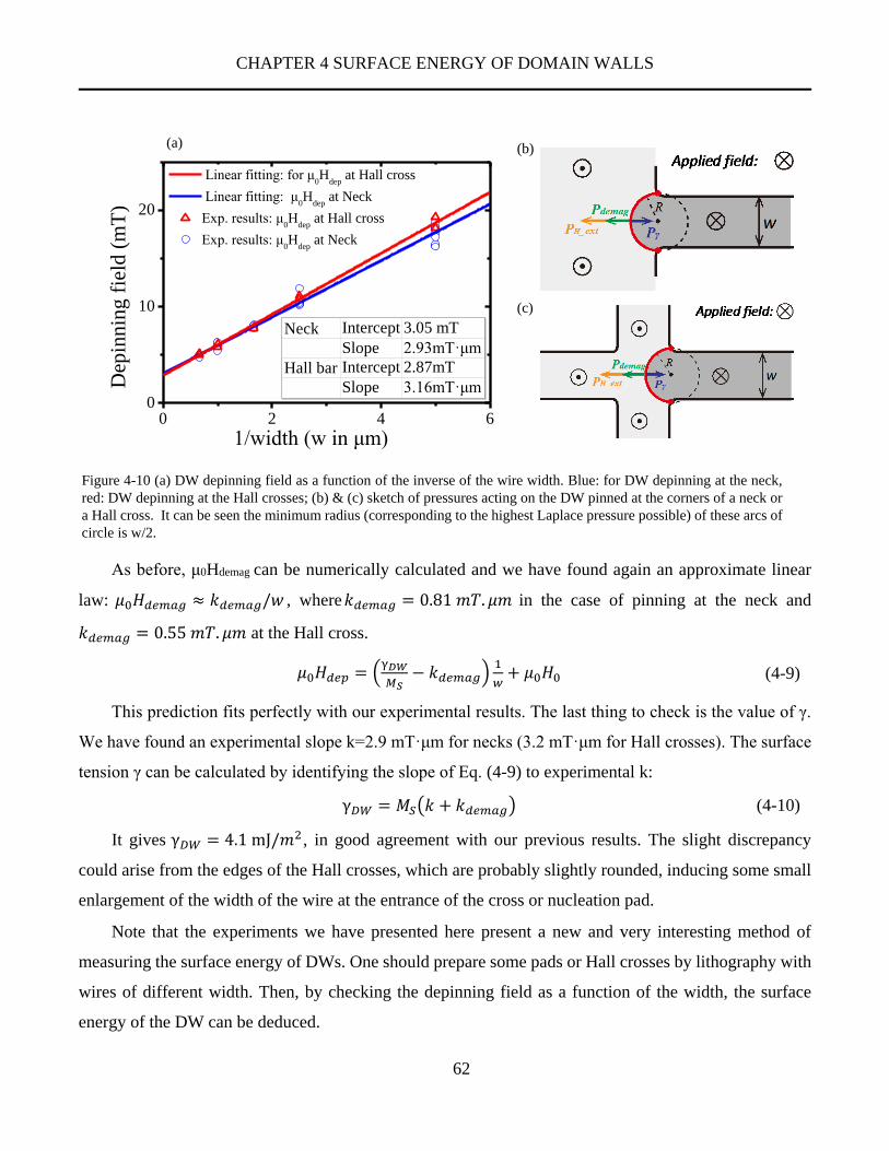
CHAPTER 4 SURFACE ENERGY OF DOMAIN WALLS
62
As before, μ0Hdemag can be numerically calculated and we have found again an approximate linear
law: 𝜇0𝐻𝑑𝑒𝑚𝑎𝑔 ≈ 𝑘𝑑𝑒𝑚𝑎𝑔/𝑤 , where𝑘𝑑𝑒𝑚𝑎𝑔 = 0.81 𝑚𝑇. 𝜇𝑚 in the case of pinning at the neck and
𝑘𝑑𝑒𝑚𝑎𝑔 = 0.55 𝑚𝑇. 𝜇𝑚 at the Hall cross.
𝜇0𝐻𝑑𝑒𝑝 = (γ𝐷𝑊
𝑀𝑆− 𝑘𝑑𝑒𝑚𝑎𝑔)
1
𝑤+ 𝜇0𝐻0 (4-9)
This prediction fits perfectly with our experimental results. The last thing to check is the value of γ.
We have found an experimental slope k=2.9 mT·μm for necks (3.2 mT·μm for Hall crosses). The surface
tension γ can be calculated by identifying the slope of Eq. (4-9) to experimental k:
γ𝐷𝑊 = 𝑀𝑆(𝑘 + 𝑘𝑑𝑒𝑚𝑎𝑔) (4-10)
It gives γ𝐷𝑊 = 4.1 mJ/𝑚2 , in good agreement with our previous results. The slight discrepancy
could arise from the edges of the Hall crosses, which are probably slightly rounded, inducing some small
enlargement of the width of the wire at the entrance of the cross or nucleation pad.
Note that the experiments we have presented here present a new and very interesting method of
measuring the surface energy of DWs. One should prepare some pads or Hall crosses by lithography with
wires of different width. Then, by checking the depinning field as a function of the width, the surface
energy of the DW can be deduced.
0 2 4 60
10
20
Linear fitting: for μ0H
dep at Hall cross
Linear fitting: μ0H
dep at Neck
Exp. results: μ0H
dep at Hall cross
Exp. results: μ0H
dep at Neck
Dep
inn
ing
fie
ld (
mT
)
1/width (w in μm)
Neck Intercept 3.05 mT
Slope 2.93mT·μm
Hall bar Intercept 2.87mT
Slope 3.16mT·μm
(a) (b)
(c)
Figure 4-10 (a) DW depinning field as a function of the inverse of the wire width. Blue: for DW depinning at the neck,
red: DW depinning at the Hall crosses; (b) & (c) sketch of pressures acting on the DW pinned at the corners of a neck or
a Hall cross. It can be seen the minimum radius (corresponding to the highest Laplace pressure possible) of these arcs of
circle is w/2.

CHAPTER 4 SURFACE ENERGY OF DOMAIN WALLS
63
Precision of the DW surface energy measured using the two approaches
Now, let us estimate the precision of the surface energy extracted based on the above two methods.
For the first method (measuring the DW surface energy based on the stabilizing field of the semicircular
domain bubble), the uncertainty mainly comes from 3 contributions:
(1) The measurement of the size of the bubble. This term is mainly determined by the resolution of
the Kerr microscope. As the radius of the bubble observed here varies from 3 μm to 10 μm and the spatial
resolution of our Kerr microscope is 500nm, the uncertainty introduced by this term is about 10% for one
point of measurement. This uncertainty has been reduced to a low level by repeating the measurements
with different sized bubbles.
(2) The magnitude of the stabilizing field. This term is mainly determined by the calibration of the
electromagnetic coil and can be reduced by a careful calibration.
(3) The calculation of the demagnetizing field. In this calculation, three parameters are involved: Ms,
tM, and Δ. The former two parameters can be precisely measured (e.g. using the vibrating sample
magnetometer or the SQUID). 𝑀𝑆 ∙ 𝑡𝑀 = 𝒎 𝑆⁄ , where m is the magnetic moments measured and S is the
Figure 4-11 The demagnetizing field as a function of the size of bubble for different DW width Δ. The
diamonds are the calculated results based on the magnetic current model and the red lines are the
linear fitting results.
0.10 0.15 0.20 0.25 0.30
0.05
0.10
0.15
0.20
0.25
0.30
0.35
0.40
0.45
Δ=5 nm
Δ=10 nm
Δ=20 nm
Dem
agnetizin
g fie
ld (
mT
)
R-1
(μm-1)
Value
Demagnetizing field
Intercept -0.0098
Slope 1.44739
Intercept 0.00212
Slope 1.24134
Intercept 7.99264E-4
Slope 1.0928

CHAPTER 4 SURFACE ENERGY OF DOMAIN WALLS
64
area of the sample measured. The calculation result of the demagnetizing field is not sensitive to Δ. As
shown in Figure 4-11, the uncertainty introduced by this term is limited within 10%. In fact, the slope of
the calculated demagnetizing field changes by less than 17% if the DW width was changed by 2 times. In
view that the contribution from the demagnetizing field to the calculation of the DW surface energy is less
than ½, the uncertainty caused by the calculation of the demagnetizing field is at a low level.
As for the second method (measurement of the DW surface energy using the depinning field at Hall
crosses or necks), uncertainties originate from three contributions:
(1) the uncertainty of the width of the wires. This may be caused by size fluctuation of the wire or
the rounded corner of the Hall cross or necks due to the nanofabrication technique. According to the
Scanning Electron Microscope (SEM) image of the sample that we studied, the corner is a little rounded,
as shown in Figure 4-12(a). This rounded corner will increase the effective width of wire that determines
the depinning field. As illustrated in Figure 4-12(b), since the surface tension is always along the tangential
direction of the DW surface and is always perpendicular to the edge of the structure, in an equilibrium
state, the endpoint of a DW should be always perpendicular to the edge of the structure, as demonstrated
by Eq.(0-21) in Appendix 1. In the critical state of depinning (corresponding to the minimum curvature
radius of the DW), the endpoints of the DW should have slid to the end of the rounded corner. If the real
width of the wire is w, because of the rounded corner, the effective width accounted for depinning is
enlarged to w+2Δw. This enlargement will cause the decrease of the measured depinning field. Compared
(a) (b)
Figure 4-12 SEM image of a studied sample. The zone displayed here is the connection part (neck) of a 1 μm wire and a
nucleation pad. We can see that the corner surrounded by red circle is a little rounded. (b) DW depinning at a structure (a
Hall cross or a neck) with rounded corner. The blue circular arc describes the DW before depinning; the red semicircular
arc describes the DW in the critical state for depinning; the green semicircular arc describes the DW after depinning.

CHAPTER 4 SURFACE ENERGY OF DOMAIN WALLS
65
with the real width, this enlargement is less important for structures with large size (e.g. 1.5μm wire) but
more important for small size (e.g. 200 nm wire). Therefore, the effect of the rounded corner will cause a
slight decrease of the slope in Figure 4-10(a) and thus lead to the underestimation of the DW surface
tension. This effect may be one reason that the result of the second method is lower by 20% than the first
method. This effect should be maximally avoided during the fabrication.
(2) The measurement of the depinning field (this term may be caused by the calibration of the
magnetic coil). In addition, the thermal activation may also introduce the uncertainty for the measurement
of the depinning field. Note that the thermal activation tends to increase the chance of depinning before
arriving at the threshold condition[49] (i.e. lead to a decrease of measured depinning field). Since the
structure with small size is more sensitive to the thermal activation due to the small activation volume[49],
the thermal activation will lead to the underestimation of the DW surface energy. In our experiments, we
have tried to reduce this effect by applying a field pulse with identic duration and the pulse is as short as
5 μs.
(3) The calculation of the demagnetizing field, as discussed above.
In summary, the first method is expected to have a better precision, with an uncertainty less than 20%.
Magnetic sensors based on the DW surface tension
In this section, we propose a novel mechanism based on the elasticity of DWs for the design of
magnetoresistive sensors: the magnetic field can be detected via the field-induced DW expansion in the
free layer of the spin valve or in the MTJ.
Concept and mechanism
As presented in the above sections, the elasticity (or the surface tension) of the DW becomes
dominant for the DW behavior in a material with weak intrinsic pinning, e.g. CoFeB. A curved DW could
contract spontaneously due to the Laplace pressure. The stabilizing field is approximately linear to the
inverse of the radius R of the semi-bubble. Moreover, the threshold field to depin the DW at the entrance
of the pad is approximately proportional to the inverse of the wire width.
Note that the propagation of the DW results in a local change of the magnetization. In the free layer
of an MTJ, this change can be accurately detected through the change of the magnetoresistance.
Interestingly, the structure near the free layer of the generally used MTJ, composed of MgO/CoFeB/heavy
metal, has got many excellent properties, which facilitate the accurate DW manipulation, for example, the
high PMA[88] and the ultralow intrinsic pinning fields[90]. We give in the following an example to show

CHAPTER 4 SURFACE ENERGY OF DOMAIN WALLS
66
the principle to measure the magnetic field using the elasticity of DWs and the method to tune the
performance of sensors through manipulating the geometry and the size of devices.
Device design and simulations
The structure of one example we proposed based on the above mechanism is shown in Figure 4-13
Structure of a sensor device proposed based on the elasticity of the DW. Two MTJs are connected via a
bridge while the pinned layer and the upper electrodes are isolated. The free layer of two or more MTJs
are connected via wire bridges while the pinned layer of MTJs are isolated. Free layers have a PMA and
magnetizations of pinned layers are perpendicularly initialized in the same direction.
Before working, opposite current pulses should be applied so that the magnetization of the free layer
of two adjacent MTJs are initialized to opposite directions via the spin transfer torque. A DW will be
created in the bridge. When the device is put in an external field, the DW will be moved in either of the
two directions, depending on the direction of the external field. At equilibrium, in an external field, the
DW is pinned at the bridge. As described by Eq. (4-5), in equilibrium, the DW will be of a circular arc
shape and the radius can be given as follows,
R =γ𝐷𝑊
2𝜇0𝑀𝑆(𝐻𝑑+𝐻𝑒𝑥𝑡) (4-11)
Figure 4-13 Structure of a sensor device proposed based on the elasticity of the DW. Two
MTJs are connected via a bridge while the pinned layer and the upper electrodes are
isolated.
Electrodes
Pinned layer
Substrate
Free layer
Barrier layer
Electrodes
MTJ 1 MTJ 2Bridge

CHAPTER 4 SURFACE ENERGY OF DOMAIN WALLS
67
Here, the demagnetizing field 𝐻𝑑 is determined by the magnetic state and the structure of the device,
varying with Hext. Other parameters are all intrinsic. Therefore, the radius of the DW arc is solely
dependent on Hext.
For a given width w of the bridge, the area reversed in the free layer caused by the expansion of the
DW can be expressed as,
S = 𝑅2 sin−1 (𝑤
2𝑅) −
𝑤
4√4𝑅2 − 𝑤2 (4-12)
The change of this area leads to the change of the magnetoresistance. In this way, the external field
is quantified through the resistance of the MTJ. Since the readout of the magnetoresistance can be realized
with very low current density, the effect of this current on the behavior of the DW can be neglected.
In order to verify the functionality of this proposed device, the response of the magnetization in the
free layer of the device versus external fields was simulated via micromagnetic using Mumax[94].
Parameters used are[90]: saturation magnetization 𝑀𝑆 = 1.1 × 10⁶ 𝐴/𝑚 , uniaxial perpendicular
anisotropy energy 𝐾𝑈 = 9.5 × 10⁵ 𝐽/𝑚3 , exchange stiffness 𝐴𝑒𝑥 = 1 × 10⁻¹¹ 𝐽/𝑚, damping constant
α=0.013. The thickness of the free layer is supposed to be 1nm.
As shown in Figure 4-14, a DW was set in the middle of the bridge as the initial state. Then a magnetic
field was applied. After the DW was pinned at the entrance, the magnitude of the magnetic field is
Figure 4-14 DW states in the free layer of two coupled MTJs: First, DW was set in the middle of the bridge of
the device. Then an external perpendicular field of -5 mT (+5 mT), -10 mT (+10 mT) was applied and the stable
state of the DW was snapshotted, respectively. At last, the external field was removed and the DW returned to
the bridge due to its elasticity. w=500 nm in this example and the width of the notch is 30 nm.
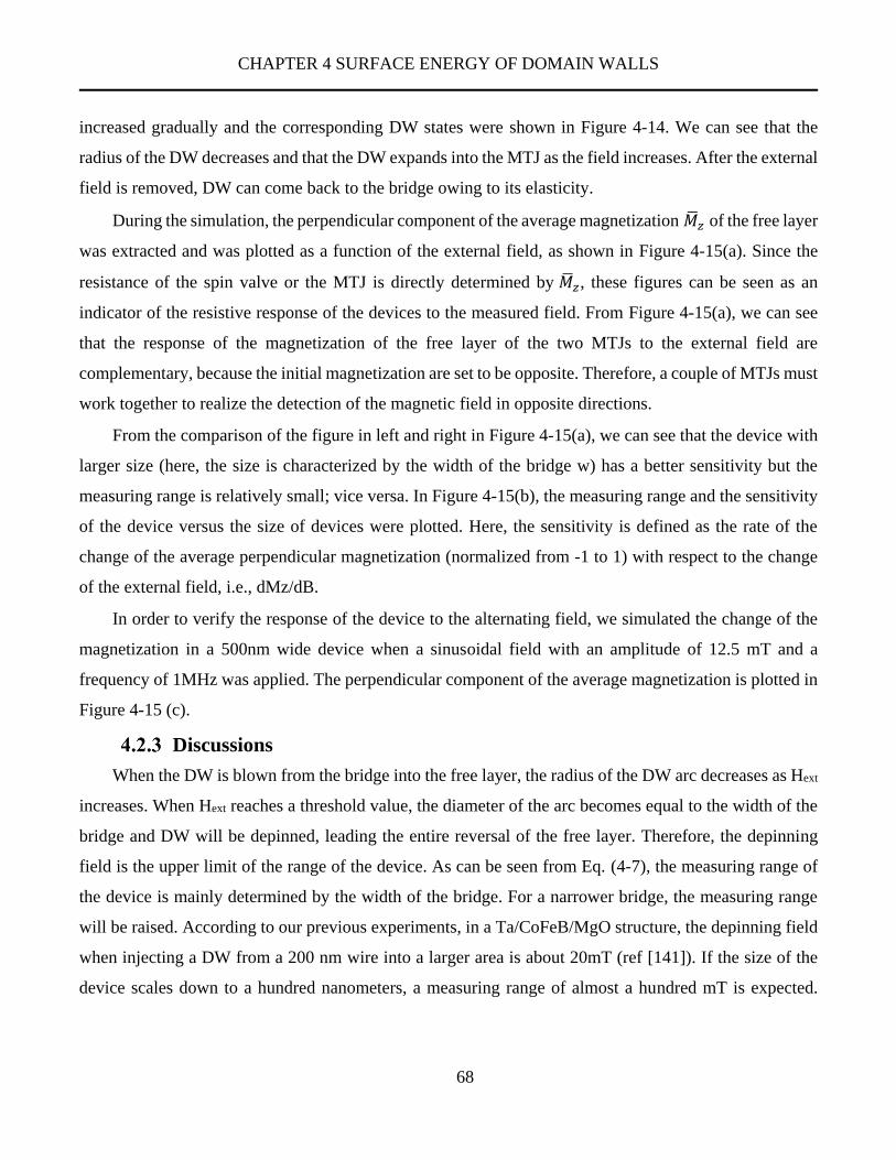
CHAPTER 4 SURFACE ENERGY OF DOMAIN WALLS
68
increased gradually and the corresponding DW states were shown in Figure 4-14. We can see that the
radius of the DW decreases and that the DW expands into the MTJ as the field increases. After the external
field is removed, DW can come back to the bridge owing to its elasticity.
During the simulation, the perpendicular component of the average magnetization �̅�𝑧 of the free layer
was extracted and was plotted as a function of the external field, as shown in Figure 4-15(a). Since the
resistance of the spin valve or the MTJ is directly determined by �̅�𝑧, these figures can be seen as an
indicator of the resistive response of the devices to the measured field. From Figure 4-15(a), we can see
that the response of the magnetization of the free layer of the two MTJs to the external field are
complementary, because the initial magnetization are set to be opposite. Therefore, a couple of MTJs must
work together to realize the detection of the magnetic field in opposite directions.
From the comparison of the figure in left and right in Figure 4-15(a), we can see that the device with
larger size (here, the size is characterized by the width of the bridge w) has a better sensitivity but the
measuring range is relatively small; vice versa. In Figure 4-15(b), the measuring range and the sensitivity
of the device versus the size of devices were plotted. Here, the sensitivity is defined as the rate of the
change of the average perpendicular magnetization (normalized from -1 to 1) with respect to the change
of the external field, i.e., dMz/dB.
In order to verify the response of the device to the alternating field, we simulated the change of the
magnetization in a 500nm wide device when a sinusoidal field with an amplitude of 12.5 mT and a
frequency of 1MHz was applied. The perpendicular component of the average magnetization is plotted in
Figure 4-15 (c).
Discussions
When the DW is blown from the bridge into the free layer, the radius of the DW arc decreases as Hext
increases. When Hext reaches a threshold value, the diameter of the arc becomes equal to the width of the
bridge and DW will be depinned, leading the entire reversal of the free layer. Therefore, the depinning
field is the upper limit of the range of the device. As can be seen from Eq. (4-7), the measuring range of
the device is mainly determined by the width of the bridge. For a narrower bridge, the measuring range
will be raised. According to our previous experiments, in a Ta/CoFeB/MgO structure, the depinning field
when injecting a DW from a 200 nm wire into a larger area is about 20mT (ref [141]). If the size of the
device scales down to a hundred nanometers, a measuring range of almost a hundred mT is expected.

CHAPTER 4 SURFACE ENERGY OF DOMAIN WALLS
69
While for a larger bridge, the measuring range decrease but the sensitivity increases, as shown in Figure
4-15 (b).
Simulation results have shown that these devices have a satisfactory performance for the detection of
the alternating field with a frequency of MHz. In fact, the response speed is limited by the DW motion
velocity in the free layer. According to our measurements (see Figure 3-23 ) in the Ta/CoFeB/MgO film,
the DW motion velocity can reach more than 5m/s soon when the applied field Hext exceeds the intrinsic
pinning field. Supposing that in a device of hundreds nm, the external field can be detected in less than
100 ns. For a lower external field, DW motion velocity is dominated by the intrinsic defects and decreases
rapidly, obeying the creep law, (Figure 2-8). Still, a movement of 100nm can be achieved in less than 1ms
when the measured field decreases to 0.5 mT, according to our experimental results. For the detection of
Figure 4-15 The average magnetization in the free layer of the device as a function of the external field. The width
of the bridge in the device simulated is 500 nm in the left and 100 nm in the right. Insets show the DW state in the
free layer. When external field exceeds the measuring range (13mT, marked in yellow), domain bubble breaks. (b)
The measuring range and the sensibility of devices as a function of the size of devices. (c) Average perpendicular
magnetization in the free layer of MTJs when an alternating field is applied. The width of the bridge in this simulation
is 500nm.
-15 -10 -5 0 5 10 15
-1
0
1
MTJ 1 MTJ 2 Average
External field (mT)
-40 -20 0 20 40
-1
0
1
External field (mT)
Mz (
No
rm.)
0 1 2-15
0
15
Time (μs)
μ0H
ext (m
T)
-1
0
1
MTJ 1 MTJ 2 Aver.
Mz (
No
rm.)
(a)
(b)
0 200 400 600 800 10000
20
40
60
80
Me
asurin
gra
ng
e(m
T)
Size of devices (nm)
Measuring range
0.0
0.02
0.04
0.06
0.08
0.1
SensitivityS
en
sitiv
ity (
mT
-1)
(c)
Bridge width: 500nm Bridge width: 100nm

CHAPTER 4 SURFACE ENERGY OF DOMAIN WALLS
70
a lower field, the wall coercivity and discontinuous domain wall motion known as the Barkhausen effect
may cause a problem. Fortunately, experiments of G. Wang et al. have demonstrated that this problem
could be well solved by applying an oscillating AC current[142].
Note that the above device is only an example to demonstrate the concept we proposed and to verify
the performance of this type of sensors. The monotonous and reversible response of the elastic DW to the
magnetic field provides a new aspect to design sensors. Another example of the design of magnetic sensors
based on the elasticity of DWs can be found in Appendix 2.
For the magnetic sensors proposed above, various devices with different size and geometry, thus with
different performance (e.g. measuring range, sensitivity etc.) can be fabricated in the same chip based on
this mechanism. No modulation of the intrinsic properties of the film, such as the PMA, is required.
Therefore, magnetic sensors based on the elasticity of DWs promise a higher integration level and a better
performance.
Conclusions
In this chapter, we have presented a series of experiments in which the DW surface tension becomes
the dominant effect, such as the spontaneous collapse of the semicircular domain bubble, the interplay of
two bubbles, the DW depinning at the Hall crosses. Two methods to quantify the DW surface energy were
proposed. At last, a novel type of magnetic sensors based on the DW surface tension (elasticity) was
proposed and verified using micromagnetic simulations.
Most of what have been presented up to now assume a perfect film without defects. It is true that
CoFeB films are really very good, but there are still some pinning defects: can these defects be neglected?
Obviously, they induce a creep behavior in 2D films, but, is it still true in nanowires?

CHAPTER 5 DOMAIN WALL MOTION AND PINNING EFFECTS IN NANOWIRES
71
Chapter 5 Domain walls motion and pinning
effects in nanowires
In this chapter, we focus on the DW dynamic behaviors in nanowires. DWs motion velocities in
nanowires induced by a magnetic field or by the combined effects of field and current have been measured.
DW pinning and depinning effects caused by the randomly distributed hard pinning sites have been
systematically studied. At last, a ring-shape racetrack memory based on the complementary work of SOT
and STT was proposed and verified via micromagnetic simulations.
Field-induced DWs motion in nanowires
Velocities of the field-induced DWs motions in 200 nm to 1.5 μm wide wires were measured using
a mini coil with a rising time of 220 ns. The measuring results are shown in Figure 5-1. The method of
measurement can be found in chapter 3.
Figure 5-1 Velocities of the field-induced DW motion measured in infinite film and
in nanowires of different width.
0 10 20
0
2
4
6
Infinite film1.5 μm1 μm600 nm400 nm200 nm
DW
velo
city
(m/s
)
μ0Happ (mT)

CHAPTER 5 DOMAIN WALL MOTION AND PINNING EFFECTS IN NANOWIRES
72
Propagation of DW in nanowires is different from the case in the infinite film, where DW can
circumvent the hard pinning sites (see Figure 2-5). In nanowire, DW can be completely trapped by a hard
pinning site. This makes the DW motion stochastic when driven by a weak magnetic field. The motion
distance depends not only on the magnitude of the applied field but also on whether hard pinning sites
exist. It is to note that the velocities measured here are based on the DW motion in the relatively smooth
section of the wire, where the DW was not completely pinned by the hard pinning sites. In addition,
measurements with the same field pulse were repeated for several times in different part of the wire and
it was always the maximum velocity observed that was kept here.
Depending on the field range, the influence of the dimension reduction is different: under a low field,
DWs move faster in broader wires; under a high field, DWs move faster in narrower wires, as shown in
Figure 5-1.
Figure 5-2 Field-induced creep motion of DWs in the nanowires. The ☆ in the inset denotes
the critical point where the DW motion velocities leave the creep regime. The corresponding
field was extracted and plotted in Figure 5-3.

CHAPTER 5 DOMAIN WALL MOTION AND PINNING EFFECTS IN NANOWIRES
73
When the driving field lowers down, the pinning effects become dominant. In a narrower wire, the
pinning effect is stronger, which will be discussed in the next section, so the velocity is smaller. We plotted
DW velocities in a logarithm form in function of H-1/4, as shown in Figure 5-2. Interestingly, although
DW can be entirely trapped by hard pinning sites, DW motion in relatively smooth sections between the
hard pinning sites can still exhibit a creep mode, except that in the 200 nm wide nanowire. This means
that intrinsic pinning effects play still an important role in DW motion in narrow wires. The lines of
ln(velocity) vs. H-1/4 shift to the left when wire width scales down. This may be caused by the roughness
of the edge[29].
Meanwhile, it can be seen that the creep regime holds to higher velocities and higher fields when
wire widths scale down. This effect can also be concluded to the friction from the edge. Here we define
the effective depinning field Hdep_eff as the critical field where DW motion leaves creep regime in wires,
as denoted by the red stars in the inset of Figure 5-2. We found that Hdep_eff increased in a linear-like mode
with the inverse of wire width, with a no negligible slope, as shown in Figure 5-3. This means that the
roughness from the edge plays an important role in DW motion and DW pinning effects in nanowires.
Furthermore, we found that the DW will be entirely stuck by the pinning sites and no motion was
observable within several ms when the applied field decreased down to a threshold value. We may call it
Figure 5-3 The effective depinning field Hdep_eff vs. the wire width, extracted from
the value denoted by the red stars ☆ in Figure 5-2.
0 1 2 3
3
4
5
6
7
Eff
ective µ
0H
de
p(m
T)
1/w (μm-1)

CHAPTER 5 DOMAIN WALL MOTION AND PINNING EFFECTS IN NANOWIRES
74
the dead field. With the scaling down of the wire width, the dead field increases. For example, in the 200
nm wire, DW motion is not possible when the applied field is lower than 6mT.
Both previous studies[90] and our experiments show that in our sample, when the applied field is
higher than 15 mT, the motion of DWs is in a precessional flow regime. In the narrow wire, the roughness
of edge can reduce the turbulence of the moving DW and thus accelerate a little the velocity. In a narrower
wire, this damping is more effective, so the DW velocity is higher[143]. Our experiments about the DWs
motion in nanowires driven by a high field is in agreement with this assumption, as shown in Figure 5-1.
Randomly distributed hard pinning sites in nanowire
To be sure to avoid artefacts arising from pinning defects, we have to check where are the strongest
pinning points on the nanowires and what are the depinning field associated.
Experiments
After nucleating a DW in the wire, pulses of small amplitudes and 5µs long were applied. We have
used the coil N°16_ext (see Table 3.1), whose rise time is as short as 220 ns (see Figure 5-4 (a)). After
one or several pulses to induce DW motion along the wire, it can be observed that the propagation can be
fully stopped (Figure 5-4 (b)(n°2&3)), indicating that the DW cannot overcome the energy potential
induced by the strong pinning sites.
After the DW is trapped in a wire, the amplitude of the pulse was increased step by step (pulse 2,
Figure 5-4 (a)), until the depinning occurs (Figure 5-4 (b)(n°4)). The minimum field that can depin the
(a) (b)
Figure 5-4 (a) Example of two field pulses with the same length and different magnitude, used to measure the DW
depinning field. (b) DW pinning and depinning in a 200 nm wire: DW moves from (image n°1) to (n°2) by a lower
field pulse 1 (12.1 mT), then trapped (n°2 and n°3), DW is depinned and continue to move from (n°3) to (n°4) by
a higher field pulse 2 (13.2 mT).
0 5 100
5
10
15
Time (μs)
Pulse 1
Pulse 2
Fie
ld (
mT
)

CHAPTER 5 DOMAIN WALL MOTION AND PINNING EFFECTS IN NANOWIRES
75
trapped DW is defined as the depinning field Hdep here. For a given pinning defect, the experiment was
repeated several times and the depinning field values were reproducible with an error bar lower than
0.3mT. In order to improve the statistics, for each width, we have studied DW motion in several nanowires
(from 3 to 6) and we have selected the five strongest pinning sites along the 50m wire.
Depinning field distribution
As an example, we give the position of the several largest pinning sites measured in a 1 μm wire and
the corresponding depinning fields Figure 5-5 (a). Typical depinning fields in our sample range from 2 to
13 mT, depending on the wire width.
The main important result of this study is the
presence of several strong pinning sites along the
wires[28,144]. This is different from the DW
depinning behaviors in the infinite film. As shown
in Figure 2-5, in 2D film, if a domain wall is pinned
at one point, it can keep on propagating on the sides,
creating a 360° domain wall, ended by a circle at
the position of the pinning. Then, because of the
Laplace pressure, the DW can overcome the
pinning. In narrow wires, there are no sides, and
strong pinning can completely prevent the DW
from moving since the wall is fully stopped at
several locations along the wires.
The origin of the hard pinning sites is difficult to figure out just by morphological observation. Figure
5-5 (b) is the profile of a 1 μm wires observed with a scanning electron microscope (SEM). No obvious
notch in the edge or visible defects on the surface of wire can be found. Here we try to explore the origin
of these hard pinning sites based on statistical analysis of the experimental data.
The distribution of the strongest depinning fields as a function of the wire width is indicated in Figure
5-6. It can be observed that the distribution is shifted towards higher values as the width of the nanowire
Figure 5-5 (a) Position of the several largest pinning sites in
a 1 μm wire. The corresponding depinning field of sites from
1-7 are: 5.2, 5.2, 6.1, 5.4, 5.5, 5.0, 4.5 (mT). (b) SEM image
of a 1 μm wide wire studied.
10 µm 1 2 3 4 5 6 7
(a)
(b)

CHAPTER 5 DOMAIN WALL MOTION AND PINNING EFFECTS IN NANOWIRES
76
is decreased. This shift can be explained by taking into account the different forces acting on the DW in
the wires. First, the pressure 2𝜇0𝐻𝑒𝑥𝑡𝑀𝑆 due to the external applied field μ0Hext integrated over the section
of the wire, gives a force 2𝜇0𝐻𝑒𝑥𝑡𝑀𝑆𝑤𝑡𝑀, where tM is the thickness of the film and w the width of the
wire[141]. Then, the presence of intrinsic pinning defects in the films induces a force FF. These intrinsic
defects alone are not strong enough to stop the DW since the magnetic fields applied for observing DW
depinning in the nanowires are much higher than those needed to move DW in the films (typically < 1mT).
The effect of intrinsic pinning effects can be described using a friction force that depends on the number
N of defects and is proportional to the section. It leads to a maximum force 𝐹𝐹𝑤𝑡𝑀, opposite to the induced
motion. Finally, the strong pinning sites evidenced here creates a pinning force FSD. Considering the action
of these three different forces, the depinning process occurs when the pressure from external field
overcomes the overall pinning forces 𝐹𝑆𝐷 + 𝐹𝐹𝑤𝑡𝑀 . The depinning field 𝜇0Hdep is deduced from this
threshold condition:
𝜇0𝐻𝑑𝑒𝑝 =𝐹𝐹
2𝑀𝑠+
𝐹𝑆𝐷
2𝑀𝑆𝑡𝑀
1
𝑤 (5-1)
It has to be noted that the quantities MS, 𝑡𝑀, FF can be assumed to be constant. However, FSD requires
a more careful analysis. Indeed, FSD is related here to the tail of the distribution of the pinning forces. As
such, the probability to get a very strong pinning force is small and increases with the overall number N
Figure 5-6 histogram distribution of depinning field obtained for the strongest defects, using the five strongest ones for each
wire included in the statistics.
CHAPTER 5 DOMAIN WALL MOTION AND PINNING EFFECTS IN NANOWIRES
77
of pinning sites. Therefore, this parameter may depend on the area and on the length of the wire as
described below.
Data analysis and the origin of the pinning effects
To describe the distribution of FSD, we have assumed it to be Gaussian and centered on zero. As the
number of pinning sites is huge, we have assumed that we have the same behavior for the average value
of the five strongest pinning sites as for the value of the strongest pinning site alone. Then, two cases can
be considered. First, the strong pinning sites are of extrinsic origin such as the roughness of the edge
introduced by the patterning process. In this case, their number should depend on the length of the edges,
which is the same for all wires, whatever the width is. Therefore, the overall number of strong defects as
well as FSD should be a constant and, according to equation (5-8), Hdep should increase linearly as a
function of 1/w.
Second, the strong pinning sites are of intrinsic origin and they originate from the magnetic films[145].
Then, their number N is proportional to the area of the wire, which means here to the width w of the wire.
In order to get a pinning force F=FM for the strongest pinning site, it means that all the other pinning sites
have a pinning force lower than FM. In this case, the probability to get F as the strongest pinning force is:
P(F = 𝐹𝑀) = N𝑃𝑁−1(𝐹𝑆𝐷 < 𝐹𝑀)𝑃(𝐹𝑀) (5-2)
Figure 5-7 Expected distribution of the strongest pinning force as a function of the overall number of defects
(N), assuming a Gaussian distribution of defects centered on zero and with standard distribution σ=1.
0 1 2 3 4 5 60
0.2
0.4
0.6
0.8
1
Pinning force
Pro
ba
bili
ty d
en
sity
N=100
N=1000
N=1000
N=10000

CHAPTER 5 DOMAIN WALL MOTION AND PINNING EFFECTS IN NANOWIRES
78
where the function P holds for the probability function. As we have assumed a Gaussian distribution,
we get the following functions for P(F ) and P( FSD< F ):
𝑃(𝐹) =1
𝜎√2𝜋𝑒𝑥𝑝 (−
𝐹2
2𝜎2) (5-3)
𝑃(𝐹𝑆𝐷 < 𝐹) = ∫1
𝜎√2𝜋𝑒𝑥𝑝 (−
𝐹2
2𝜎2)𝐹
0𝑑𝐹 = erf (
𝐹
√2𝜎) (5-4)
Injecting Eq. (5-10) and (5-11) in Eq. (5-9), the distribution probability of FM for several values of N
can be simulated, as seen in Figure 5-7. It can be observed that the average value of expected FM is shifted
towards the high values as N increases. To get a meaningful shift, there must a quite large increase of N.
For instance, when N is multiplied by ten, the increase of FM is around 20%. In our experiment, the width
goes from 200 nm to 1.5 µm, which is almost a factor of ten. Furthermore, for the strongest intrinsic
pinning effect in a wire, the pinning may be caused by the resultant force of two or several pinning sites
that coincidently cluster. This cluster of pinning sites range along the transverse direction of wire and
behavior as a single solid pinning site. For a wider wire, the probability of having such clusters is larger
than that in a narrower wire. As a result, the decrease of the expected FM should be much larger than 20%
as w increases from 200nm to 1.5 μm. Noting that, from Eq. (5-8), FSD determines the slope of this function.
If FSD decreases as 1/w, the slope of the curve should drop down when 1/w increases and the relation
Figure 5-8 Depinning fields of the strongest defects experimentally
obtained as a function of 1/w, where w is the width of the wire.
0 2 4 60
5
10
15
De
pin
nin
gF
ield
(mT
)
1/w (μm-1)
3.2
Exp. results
Linear fitting
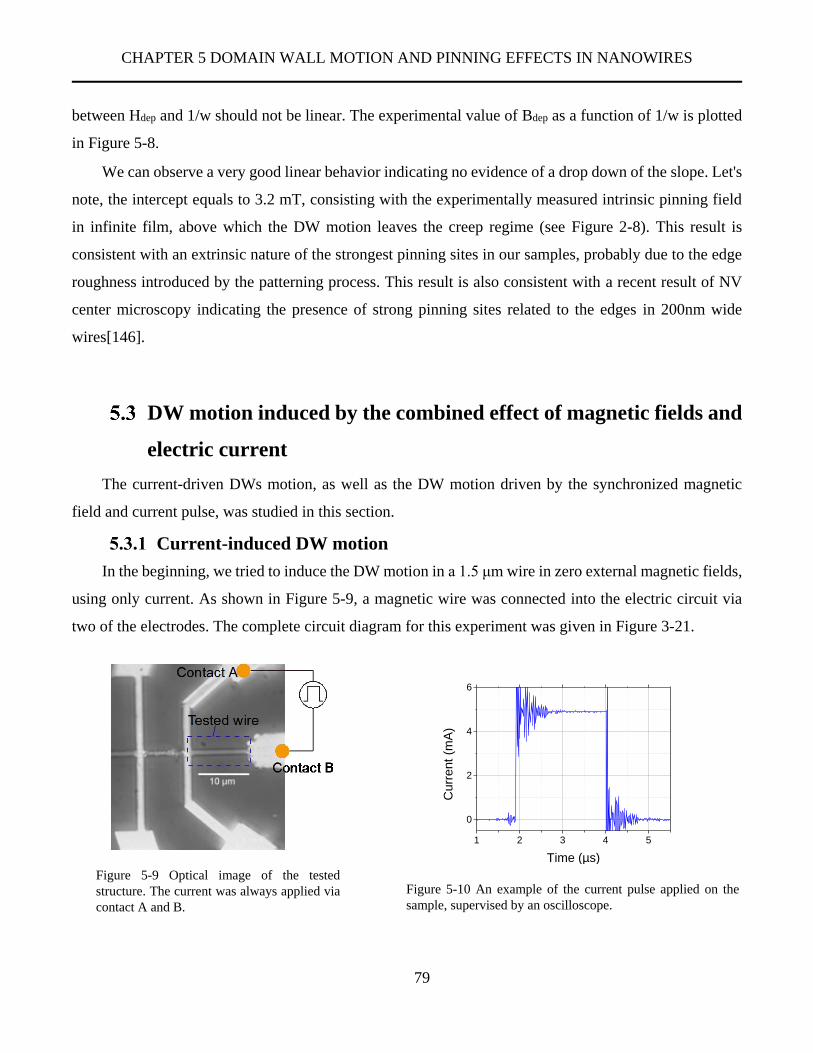
CHAPTER 5 DOMAIN WALL MOTION AND PINNING EFFECTS IN NANOWIRES
79
between Hdep and 1/w should not be linear. The experimental value of Bdep as a function of 1/w is plotted
in Figure 5-8.
We can observe a very good linear behavior indicating no evidence of a drop down of the slope. Let's
note, the intercept equals to 3.2 mT, consisting with the experimentally measured intrinsic pinning field
in infinite film, above which the DW motion leaves the creep regime (see Figure 2-8). This result is
consistent with an extrinsic nature of the strongest pinning sites in our samples, probably due to the edge
roughness introduced by the patterning process. This result is also consistent with a recent result of NV
center microscopy indicating the presence of strong pinning sites related to the edges in 200nm wide
wires[146].
DW motion induced by the combined effect of magnetic fields and
electric current
The current-driven DWs motion, as well as the DW motion driven by the synchronized magnetic
field and current pulse, was studied in this section.
Current-induced DW motion
In the beginning, we tried to induce the DW motion in a 1.5 μm wire in zero external magnetic fields,
using only current. As shown in Figure 5-9, a magnetic wire was connected into the electric circuit via
two of the electrodes. The complete circuit diagram for this experiment was given in Figure 3-21.
1 2 3 4 5
0
2
4
6
Curr
ent
(mA
)
Time (µs)
Figure 5-10 An example of the current pulse applied on the
sample, supervised by an oscilloscope.
Figure 5-9 Optical image of the tested
structure. The current was always applied via
contact A and B.
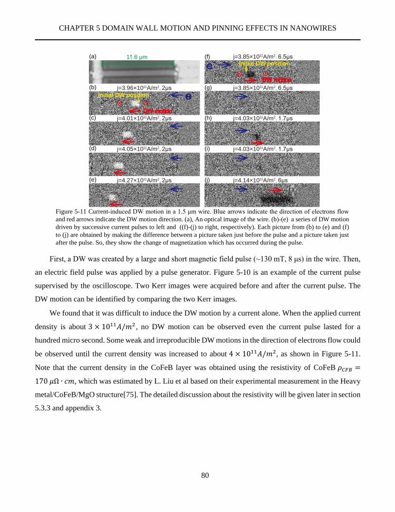
CHAPTER 5 DOMAIN WALL MOTION AND PINNING EFFECTS IN NANOWIRES
80
First, a DW was created by a large and short magnetic field pulse (~130 mT, 8 μs) in the wire. Then,
an electric field pulse was applied by a pulse generator. Figure 5-10 is an example of the current pulse
supervised by the oscilloscope. Two Kerr images were acquired before and after the current pulse. The
DW motion can be identified by comparing the two Kerr images.
We found that it was difficult to induce the DW motion by a current alone. When the applied current
density is about 3 × 10¹¹𝐴/𝑚2 , no DW motion can be observed even the current pulse lasted for a
hundred micro second. Some weak and irreproducible DW motions in the direction of electrons flow could
be observed until the current density was increased to about 4 × 10¹¹𝐴/𝑚2, as shown in Figure 5-11.
Note that the current density in the CoFeB layer was obtained using the resistivity of CoFeB 𝜌𝐶𝐹𝐵 =
170 𝜇Ω ∙ 𝑐𝑚, which was estimated by L. Liu et al based on their experimental measurement in the Heavy
metal/CoFeB/MgO structure[75]. The detailed discussion about the resistivity will be given later in section
5.3.3 and appendix 3.
Figure 5-11 Current-induced DW motion in a 1.5 μm wire. Blue arrows indicate the direction of electrons flow
and red arrows indicate the DW motion direction. (a), An optical image of the wire. (b)-(e) a series of DW motion
driven by successive current pulses to left and ((f)-(j) to right, respectively). Each picture from (b) to (e) and (f)
to (j) are obtained by making the difference between a picture taken just before the pulse and a picture taken just
after the pulse. So, they show the change of magnetization which has occurred during the pulse.
j=4.01×10¹¹A/m2 2μs
j=4.05×10¹¹A/m2 2μs
j=4.27×10¹¹A/m2 2μs
j=3.96×10¹¹A/m2 2μs
j=4.03×10¹¹A/m2 1.7μs
j=4.03×10¹¹A/m2 1.7μs
j=4.14×10¹¹A/m2 6μs
j=3.85×10¹¹A/m2 6.5μs
j=3.85×10¹¹A/m2 6.5μs11.6 μm (f)
(g)
(h)
(i)
(j)
(a)
(b)
(c)
(d)
(e)
Initial DW position
Initial DW position

CHAPTER 5 DOMAIN WALL MOTION AND PINNING EFFECTS IN NANOWIRES
81
Surprisingly, as the density of the applied
current increased to about 4.5 × 10¹¹𝐴/𝑚2 , the
direction of DW motion becomes stochastic, as shown
in Figure 5-12.
Next, we further increased the density of applied
current. We found a more strange behavior of the DW
in this tested wire. As shown in Figure 5-13, when the
density of the applied current reached a critical value
(about 4.5 × 10¹¹𝐴/𝑚2) the final position of the DW
was not determined by the direction of applied current
or the initial DW configuration (⨀|⨂ or ⨂|⨀ ). The
DW always move to the right and disappeared into the
electrode in the right end. Here, we just note this
confusing phenomenon and cannot give an
appropriate explanation.
Figure 5-12 The current-induced stochastic motion of
DW in the 1.5 μm wide wire. The direction of the
electron flow were always to the left in this
experiment. Each picture are obtained by making the
difference between a picture taken just before the
pulse and a picture taken just after the pulse. So, they
show the change of magnetization which has occurred
during the pulse.
j=4.45×10¹¹A/m2, 2μs
j=4.36×10¹¹A/m2, 2μs
j=4.37×10¹¹A/m2, 2μs
j=4.48×10¹¹A/m2, 2μs
j=4.50×10¹¹A/m2, 2μs
j=4.50×10¹¹A/m2, 2μs
j=4.50×10¹¹A/m2, 2μs
Initial DW position
DW motion

CHAPTER 5 DOMAIN WALL MOTION AND PINNING EFFECTS IN NANOWIRES
82
DWs motion induced by synchronized current pulses and magnetic field
pulses
Since the DW is difficult to be moved by a low current and the DW behavior induced by a high
current is irregular, we begin to search for the regular and reproducible DW motions induced by the
combined effects of magnetic field and electrical current pulse.
Figure 5-13 DW motion induced by a relatively high current. (a-d), DW move always to the right and disappeared
into the electrode in the right end, no matter the initial state of DW or the direction of the applied current. (e,f), if
the magnetization of the wire is initially saturated, i.e., no DW exists, there is no change in the magnetization
even the current pulse last for 50 μs. For each group of picture, the first pictures show the magnetic state (a
saturated reference have been used to get the magnetic picture), while the second show the change of
magnetization (difference between pictures acquired just before and just after the pulse).
j=4.95×10¹¹A/m2 12μs
j=4.81×10¹¹A/m2 6.5μs j=4.63×10¹¹A/m2 2μs j=4.82×10¹¹A/m2 7μs
j=4.72×10¹¹A/m2 50μs j=4.72×10¹¹A/m2 50μs
e-
DW
Initial DW state Initial DW state
Initial DW state Initial state: saturated Initial state: saturated
(a) (b) (c)
(d) (e) (f)

CHAPTER 5 DOMAIN WALL MOTION AND PINNING EFFECTS IN NANOWIRES
83
Experiments and results
The width of the wire tested here is 1.5 μm, as shown in Figure 5-14. After the DW nucleation, the
synchronized magnetic field pulse and current pulse were applied. Figure 5-15 shows an example of the
field pulse and current pulse supervised by an oscilloscope. A small delay between the field and the current
was set, so that, the magnetic field had reached its plateau when the current started to flow in the wire.
We found that, compared with DW motions
induced by the magnetic field alone, the DW
motion velocity was changed obviously when the
current is introduced. The DW motion was
accelerated in the direction of the electrons while
it was slowed down when the DW motion is
opposite to the direction of the electron flow, as
shown in Figure 5-16.
Velocities of DW motion with different
current density and perpendicular field were
measured systematically, as shown in Figure 5-17.
One can find that the DW velocity is obviously
accelerated in the direction of electrons in the
plateau (i.e., the DW motion when 𝜇0𝐻⊥ ≥
2 4 60
5
10
15
Fie
ld (
mT
)
Time (μs)
Field
0
2
4
6 Current
Cu
rre
nt
(mA
)
Figure 5-15 an example of the synchronized electric current
pulse and magnetic field pulse applied on the tested sample.
These pulses are supervised by an oscilloscope.
Figure 5-14 Optical image of the 1.5 wide wire
tested and the configuration of electric
measurement.
Figure 5-16 DWs motion in a 1.5 μm wide wire induced by
synchronized magnetic field pulses and current pulses. An
external field of 14 mT and 3μs was applied along the
perpendicular direction. A current pulse of 3.7 mA was
applied synchronously in the left direction (a) and in right
direction (c). No current was applied in (b).
e-
e-
μ0H : 14 mT(a)
(b)
(c)
Initial DW position
Final DW position

CHAPTER 5 DOMAIN WALL MOTION AND PINNING EFFECTS IN NANOWIRES
84
14 mT). However, DW velocities decrease and become stochastic for a lower driving field (creep regime
and depinning transition mode) when current is introduced, no matter the direction of the current. In fact,
during the measurements, we found that the DW pinning effect is obviously enhanced when a current is
introduced. The larger the current is, the stronger the pinning effects are. This phenomenon will be
discussed in section 5.4 .
Now, let us first analyze the DW motion velocity in the plateau, i.e. for the driving field in the range
from 14 mT to 25 mT. According to Eq.(2-26) and a damping constant α=0.013 [90], the Walker
breakdown field of this sample is about 𝜇0𝐻𝑊 = 𝛼𝜇0𝑀𝑆/2 = 0.8 mT for the field-driven DW motion.
This value is far smaller than 14mT and is masked by the creep motion. When a current is introduced, the
Walker breakdown has not occurred. We can tell that the plateau of velocity we see here is in fact in the
precessional flow mode. Since the DW motion velocity in this range remains stable, we did an average on
the velocities (enclosed in green dashed line in Figure 5-17) for each current and plotted the mean
velocities as a function of the applied current, as shown in Figure 5-18. A very good linear relationship
between the DW velocity and the magnitude of the applied current was obtained. After a linear fitting, an
Figure 5-17 DW motion velocities induced by different fields and current densities. Current
flowing along the field-induced DW motion direction is defined as positive. Velocities in the
plateau, boxed by the dashed green line, is averaged and the plotted as a function of the current in
Figure 5-18

CHAPTER 5 DOMAIN WALL MOTION AND PINNING EFFECTS IN NANOWIRES
85
intercept of 4.9 m/s is obtained. This term is DW velocity induced by the magnetic field alone. The slope
represents the contribution from the current induce motion.
Discussions
In the precessional mode, the azimuth angle φ of magnetization in the center of DW �⃗⃗� 𝐷𝑊 alternates
from 0 to 2π, and the sin𝜑̅̅ ̅̅ ̅̅ ̅ = 0 (the same for cosφ and sin2φ). Moreover, the DMI is very weak in this
sample, here, to begin with, we assume SOT negligible. The current-induced part is mainly contributed
by the STT. By neglecting the pinning potential, the 1D model described by Eq.(2-43)- (2-45) can be
reduced to be [61,83],
�̇� +𝛼
𝛥�̇� = 𝛾0𝐻𝑍 +
𝜉𝑢
∆ (5-5)
−α�̇� +�̇�
Δ=
𝛾0𝐻𝐾
2+ 𝑠𝑖𝑛 2𝜑
𝑢
Δ (5-6)
By assuming sin 2𝜑̅̅ ̅̅ ̅̅ ̅̅ = 0, we can get,
𝑣𝑆𝑇𝑇+𝐵 = 𝑣𝑆𝑇𝑇 + 𝑣𝐵 (5-7)
Figure 5-18 Average velocities obtained based on the results in Figure 5-17 (enclosed in green). The
error bar was taken as the standard deviation. The red line is a linear fitting on all these velocities.
The current density in the CoFeB layer estimated using ρCFB=170 μΩ·cm.
-4 -2 0 2 4
-4
-2
0
2
4
6
8
10
12
Average DW velocity in plateau (exp.)Linear fitting
DW
ve
locity (
m/s
)
Current density (1011
A/m2)
Slope: -1.36x10⁻¹¹ (m/s)/(A/m2)
Intercept: 4.9 m/s

CHAPTER 5 DOMAIN WALL MOTION AND PINNING EFFECTS IN NANOWIRES
86
With
𝑣𝑆𝑇𝑇 =1+𝛼𝜉
1+𝛼2 ∙𝜇𝐵𝑃
𝑒𝑀𝑠𝑗𝑆𝑇𝑇 (5-8)
where P is the spin polarization of the magnetic material and 𝑗𝑆𝑇𝑇 is the current density in magnetic
layer. In view that α ≪ 1, 𝑣𝑆𝑇𝑇 can be approximated to,
𝑣𝑆𝑇𝑇 =𝜇𝐵𝑃
𝑒𝑀𝑠𝑗𝑆𝑇𝑇 (5-9)
Now, our results confirmed the above analysis: the DW motion velocities in the precessional flow
mode under the combined effect of the STT and the magnetic field pulse is the sum of the velocities that
induced by either of these driving forces alone.
Polarization of CoFeB in the Ta/CoFeB/MgO structure
In fact, the relationship described in Eq. (5-7) has been observed in some experiment performed on
the material with the in-plane anisotropy such as the permalloy[13,147,148] or on the [CoNi]n superlattice
with PMA[149]. However, to our knowledge, it is the first time that this relationship is observed in the
heavy metal/ferromagnet/insulator multilayers. In such a multilayer, some part of the current flows in the
Ta layers, which is not magnetic.
In the presented model, the important parameter is the current density in the ferromagnetic layer,
which cannot be deduced as simply as in the previous cases, for which all the conductive layers were
ferromagnetic. How to get the meaningful density of
current?
Indeed, for the structure composed of ultra-thin films,
such as the Ta/CoFeB/MgO/Ta studied here (Figure 5-19),
it is difficult to identify the current flowing in each layer
because in such thin films without isolation in the interface,
conducting electrons are not constrained in specified
layers. They diffuse among different layers and go forward
with a non-straight trajectory due to scatterings.
One may count the proportion of the current for each layer according to their conductivity. Under
such an assumption, the effective current flowing in the FM layer can be estimated as,
𝑗𝑆𝑇𝑇 =𝑅
𝑙𝜌𝐶𝐹𝐵𝐼𝐶 (5-10)
Figure 5-19 Sketch of the structure of the
multilayers studied.

CHAPTER 5 DOMAIN WALL MOTION AND PINNING EFFECTS IN NANOWIRES
87
where R and l are the resistance and the width of the wire connected into the electric circuit, 𝜌𝐶𝐹𝐵 is the
resistivity of the CoFeB and Ic is the current flowing the whole section of the wire. For the wire tested
here, R=5.2 kΩ, l=33.3 μm. Now, the estimation of the resistivity of the CoFeB thin film becomes the key
point.
According to the published litteratures[75,78,150] (see also the Appendix 2), the resistivity of CoFeB
layer in similar structures have been found between 160 and 330 μΩ·cm. From these results and our own
tests (see Appendix 3), we have assumed a resistivity of 170 µΩ·cm for CFB and 190µΩ·cm for Ta. Using
the Eq. (5-10), the current density in the CoFeB layer 𝑗𝑆𝑇𝑇was estimated, and the dependence of the DW
velocities on 𝑗𝑆𝑇𝑇 was replotted, as shown in Figure 5-18. A slope 𝑘 = −1.36 × 10⁻¹¹ (𝑚/𝑠) (𝐴/𝑚2)⁄
was obtained.
According to Eq. (5-9), this slope is,
𝑘 =𝜇𝐵𝑃
𝑒𝑀𝑠 (5-11)
Then, we can get the polarization of CoFeB in this structure: P= 26%.
The polarization obtained by measuring the in-plane current-induced DW motion is much lower than
the polarization measured through the Point-Contact Andreev Reflection (65%)[151] or through the
superconducting tunneling spectroscopy (53%)[91–93] in the heavy metal/CoFeB/Oxide layer structure.
The low polarization measured through the STT induced DW motion in Ta/CoFeB/MgO structure
may be caused by the following reasons. First, the spin injection into the CoFeB layer or spin accumulation
at the CoFeB/Ta interface due to spin Hall effects may reduce the spin polarization of CoFeB. Second,
because of the scatterings of electrons, conductive electrons will interpenetrate between the Ta layer and
Figure 5-20 Sketch of the electrons transport in the Ta/CoFeB/MgO multilayers
structure.
MgO
CFB
Ta
DW

CHAPTER 5 DOMAIN WALL MOTION AND PINNING EFFECTS IN NANOWIRES
88
CoFeB layer, as illustrated in Figure 5-20. The diffusion of electrons from Ta layer may reduce the spin
polarization of CoFeB. Third, scatterings of electrons in the MgO/CoFeB interface and CoFeB/Ta
interface may decay the polarization.
Note that we have found that it was difficult to observe the DW motion driven by electric current
along in this structure. The low polarization in the structure CFB/Ta may be one of the reasons to explain
this difficulty.
Enhancement of DW pinning effects by spin hall current
In our experiments, we have found that under a low driving field (BZ <10 mT), the DW motion
velocity was lowered down and becomes stochastic when a current was introduced, irrespective of the
relative direction of the DW motion to the current direction, as shown in Figure 5-17. It seems that this
reduction of velocity is caused by the enhanced pinning effects. To address this issue, we further
experimentally characterized the pinning effects in the narrow wire when a current was applied together
with the field.
Experiments and results
As stated before, we can nucleate and move a DW to any part of the wire with a short field pulse.
When DW is propagating along the wire, it can be completely stopped by a pinning site. The minimum
value to depin the DW has been defined as the depinning field Hdep. Here, we measured the DW depinning
field of the strong pinning sites in a 1.5 μm wide and 30 μm long wire when a current was applied
simultaneously. Figure 5-21 gives two examples of these measurements. The applied current changed
Figure 5-21 The pinning and depinning of the DW in a 1.5 μm wire. The direction of the electron flow is always
to the left. (a) & (c), DW moves after a lower field pulse and then pinned at the pinning site (violet arrow). (b) &
(d), DW continues to move after increasing the magnitude of the field pulse. Red arrows: direction of DW motion;
yellow arrows: initial DW position; green arrows: position of pinning sites.
(a)
(b)
(c)
(d)
10 μme-
B :
B :
B :
B :

CHAPTER 5 DOMAIN WALL MOTION AND PINNING EFFECTS IN NANOWIRES
89
from 0 to 300 GA/m2. The depinning
fields for both DW motion direction
were measured and the position of
these pinning sites are noted. Both
depinning field of the ⨀|⨂ and ⨂|⨀
DWs were measured. All the pulses
applied in this experiment were 5 μs.
More detailed information about this
measurement can be found in
Appendix 4.
The measured DW depinning
fields without current have been
plotted in Figure 5-22(a). The
abscissa axis represents the
longitudinal position of the pinning
sites and the height of the bar holds
for the amplitude of the depinning
field. The sign of the field driving
DWs to right is defined as positive
and that to left is negative. We can
find that the depinning field of the
several largest pinning sites along the
wire is about 5mT without applied
current.
DW depinning fields of the
several largest pinning sites when a
current was applied were shown in
Figure 5-22 (b)-(d). We found that the
observed pinning effects were
enhanced. In addition, several
characteristics could be found: (i), the
Figure 5-22 The position and the corresponding depinning field of the
largest pinning sites in a 1.5 μm wide 30 μm long wire in different cases.
The blue arrows denote the direction of current. The inset short wires
denote the configuration and the tilting direction of DW. The small red
triangle denotes the edge on which the extrinsic pinning effects are
enhanced. The pink number is the index of the pinning sites, which will
be referred by the analysis in the Annex 3.

CHAPTER 5 DOMAIN WALL MOTION AND PINNING EFFECTS IN NANOWIRES
90
depinning field increases as the density of the applied current increases, irrespective of the direction of
DW motion or the DW configuration (i.e., ⨀|⨂ or ⨂|⨀); (ii), the enhancement of pinning effects are
stronger for DW motion in the direction of charge current; (iii), pinning effects for DW motions in
different directions or for different DW configurations are not very correlative when the current presents.
For example, the pinning site n°2 is not so large in the case of Figure 5-22 (c) but becomes the hugest
pinning sites in the case of (d); the pinning site n°8 is the hardest pinning site in the case (c) but disappeared
in case (d). Note that according to our previous experiments, in the case without applied current, the
deviation of the DW depinning field for a specified pinning site in different measurements is not so large.
When a current 𝑗𝐶 = 3.0 × 10¹¹𝐴/𝑚2 was applied, the average value of DWs depinning field
increased by 3 -5 mT. Here, jC indicates the average current density in the Ta(5nm)/CFB(1nm) layer,
calculated using Eq. (5-10) and the average resistivity of 190 μΩ. We have numerically calculated the
perpendicular component of the Oersted field based on the Biot-Savart law, by assuming that the current
distributes uniformly along the transverse section of the multilayer strip. For a test current I=3.7 mA
(corresponds to 𝑗𝐶 = 3.0 × 10¹¹𝐴/𝑚2 in Ta/CFB layers), perpendicular component of the Oersted field
is shown in Figure 5-23. We found it to be less than
2.2 mT in the FM layer even closed to the edge.
Moreover, the direction of the perpendicular
component of the Oersted field is opposite in the
two edge. Therefore, it could not be responsible to
such an increase of the depinning field. Let's note,
we acquired a Kerr image of the sample when a
current 𝑗𝐶 = 6 × 10¹¹𝐴/𝑚2 was being applied
permanently and found that the contrast of the Kerr
image did not show an observable fading,
suggesting that the magnetization does not change
due to Joule heating in the framework of these
experiments.
Influence of the SH current on the DW depinning process
For current-induced DW motion in a wire with the HM/FM/Oxide structure, several effects could be
involved in this dynamic. First, there is the STT [132] by the current flowing in the FM layer, which can
Figure 5-23 The perpendicular component of the Oersted
field as a function of the transverse position in a 1.5 μm
wire. The calculation is based on the Biot-Savart law,
assuming that a current I=3.7 mA (corresponds to a
density of jC=300 GA/m2in the CoFeB layer) is
homogenous in the transverse direction of the wire. The
thickness of the wire is supposed to be infinitely thin.
Value in the edge, i.e. y=±0.75 μm was not given because
the calculation is not convergent here.
-0.6 -0.4 -0.2 0 0.2 0.4 0.6-3
-2
-1
0
1
2
3
Y coordinate (μm)
Oe
rste
d f
ield
(m
T)

CHAPTER 5 DOMAIN WALL MOTION AND PINNING EFFECTS IN NANOWIRES
91
move the DW in the direction of electrons flow. Considering that the enhancement of pinning effect
observed in our experiments occurred irrespective of the relative direction of the DW motion and the
current direction, it could not be caused by the STT. Second, the spin Hall current from the HM will induce
two torques, namely, the damping like SOT (DL-SOT) and field like SOT (FL-SOT)[73]. According to
Eq.(2-40), the effective fields associated with these torques can be expressed as,
�⃗⃗� 𝑆𝐻 = −ℏ𝜃𝑆𝐻𝑗𝐻𝑀
2𝑒𝑀𝑠𝑡𝑀(𝜎 𝑆𝐻 × �⃗⃗� ) (5-12)
Where 𝜎 𝑆𝐻 is the polarizing direction of the SH current. The magnitude of SH angle 𝜃𝑆𝐻 depends on the
composition and lattice structure of HM. In the β phase Ta, 𝜃𝑆𝐻 can reach a value as large as 0.12, with a
negative sign [69,75] (see also the Table 2-1). The FL-SOT has been evidenced to be several orders
smaller than the DL-SOT[73]. In materials without DMIs, such as the sample studied here, the DW is of
Bloch type. If the DW is aligned along the transverse direction i.e. y-direction, the magnetization in the
center of DW �⃗⃗� 𝐷𝑊 is also aligned along the transverse direction, parallel to 𝜎 𝑆𝐻. According to Eq.(2-40)
the torque induced by the SH current is zero. However, in the case of the DW pinning, �⃗⃗� 𝐷𝑊 is not always
along the transverse direction because of the curvature of the DW surface. Thus, the influence of the SH
current on the DW is no longer zero. As shown in Figure 5-24, the effective field generated by the SH
current �⃗⃗� 𝑆𝐻 can be parallel or opposite to the externally applied field �⃗⃗� 𝑒𝑥𝑡 , depending on the tilting
direction of �⃗⃗� 𝐷𝑊. This effect must be considered carefully.
In the following, we investigate the influence of the SH current on the DW pinning effects using
micromagnetic simulations, which may provide a possible explanation for the enhancement of pinning
(a)
(
b)
(b)
Figure 5-24 DL-SOT imparted by the SH current and the associated effective field in cases of different DW tilting
direction.
z
x
y
τSH
τHext
HSH
Hext
Spin Hall
current
φ
z
x
y
τSH
τHext
HSH
Hext
current
φ

CHAPTER 5 DOMAIN WALL MOTION AND PINNING EFFECTS IN NANOWIRES
92
effects observed in our experiments. Here, we divide the DW pinning effects into two types: one type is
caused by the isolated hard pinning sites. This effect may arouse from the large defects on the edge of the
wires introduced during the nanofabrication (commonly called as extrinsic pinning effects) or a single
hard pinning in the wire. Another type is caused by the collective pinning effect of small and densely
distributed defects in the wire, which arouse from the random inhomogeneities of the magnetic film
(commonly called intrinsic pinning effects of the magnetic film).
Influence of the SH current on the isolated pinning effects
First, the influence of the SH current on the isolated pinning effects, including the pinning effects
caused by the huge defects along the edge or caused by
an isolated huge defect in the wire, is studied.
The DW depinning process was simulated using
MuMax code[94,152]. The simulation is based on the
Landau–Lifshitz–Gilbert equation in which the
Slonczewski torque by the SH current is included. As
shown in Figure 5-25, we introduced a defect in the edge
of a 1 μm wide wire by creating a triangular notch (70
nm deep) or inside the wire by creating a circular hole (a
diameter of 50 nm). Figure 5-25(a) and (b) show the DW
profile when a perpendicular field was applied while the
SH current was zero; in Figure 5-25 (c)-(f), a
perpendicular field and a pure spin current polarized
along the +y (up) direction with a density 𝑗𝑃 = 3 ×
1010𝐴/𝑚2 were applied.
From the simulation results, we can find that in the
absence of SH current, the DW is of Bloch type and the
spiral of the DW alternates, separated by the so-called
Bloch points. While �⃗⃗� 𝐶𝐷𝑊 switches to +y direction
when the SH current is introduced. When the DW is
Figure 5-25 The profile of the pinned DWs in different
cases (by simulations). Red: �⃗⃗� in ⊙ direction; blue: ⊗.
The black arrow indicate the direction of �⃗⃗� 𝐷𝑊 . Each
picture is acquired just before or during the DW depinning
process. The size of each figure is 1 μm×1 μm. The depth
of the notch in (a)(c)&(d) is 70 nm. The diameter of hole in
(b)(e)&(f) is 50 nm. Other parameters: MS=1.1x10⁶A/m3,
Aex=25pJ/m, Ku=9.9×10⁵J/m3, no DMI, no STT.
x
y
z
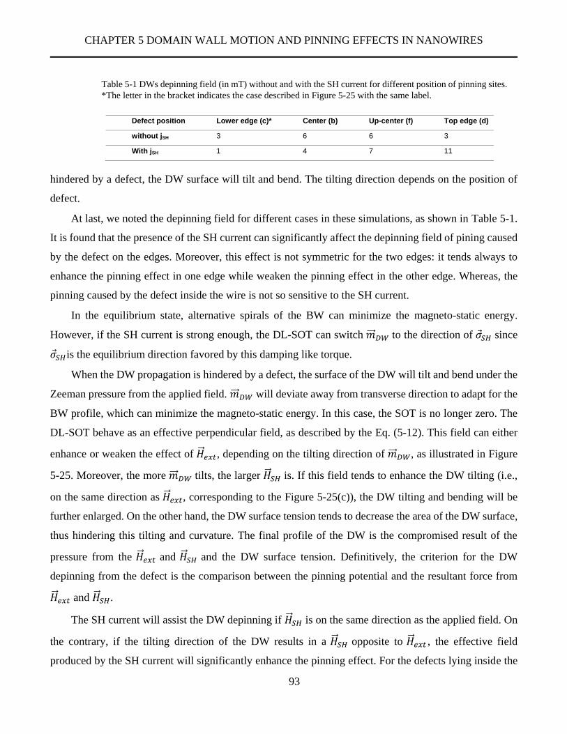
CHAPTER 5 DOMAIN WALL MOTION AND PINNING EFFECTS IN NANOWIRES
93
hindered by a defect, the DW surface will tilt and bend. The tilting direction depends on the position of
defect.
At last, we noted the depinning field for different cases in these simulations, as shown in Table 5-1.
It is found that the presence of the SH current can significantly affect the depinning field of pining caused
by the defect on the edges. Moreover, this effect is not symmetric for the two edges: it tends always to
enhance the pinning effect in one edge while weaken the pinning effect in the other edge. Whereas, the
pinning caused by the defect inside the wire is not so sensitive to the SH current.
In the equilibrium state, alternative spirals of the BW can minimize the magneto-static energy.
However, if the SH current is strong enough, the DL-SOT can switch �⃗⃗� 𝐷𝑊 to the direction of 𝜎 𝑆𝐻 since
𝜎 𝑆𝐻is the equilibrium direction favored by this damping like torque.
When the DW propagation is hindered by a defect, the surface of the DW will tilt and bend under the
Zeeman pressure from the applied field. �⃗⃗� 𝐷𝑊 will deviate away from transverse direction to adapt for the
BW profile, which can minimize the magneto-static energy. In this case, the SOT is no longer zero. The
DL-SOT behave as an effective perpendicular field, as described by the Eq. (5-12). This field can either
enhance or weaken the effect of �⃗⃗� 𝑒𝑥𝑡, depending on the tilting direction of �⃗⃗� 𝐷𝑊, as illustrated in Figure
5-25. Moreover, the more �⃗⃗� 𝐷𝑊 tilts, the larger �⃗⃗� 𝑆𝐻 is. If this field tends to enhance the DW tilting (i.e.,
on the same direction as �⃗⃗� 𝑒𝑥𝑡, corresponding to the Figure 5-25(c)), the DW tilting and bending will be
further enlarged. On the other hand, the DW surface tension tends to decrease the area of the DW surface,
thus hindering this tilting and curvature. The final profile of the DW is the compromised result of the
pressure from the �⃗⃗� 𝑒𝑥𝑡 and �⃗⃗� 𝑆𝐻 and the DW surface tension. Definitively, the criterion for the DW
depinning from the defect is the comparison between the pinning potential and the resultant force from
�⃗⃗� 𝑒𝑥𝑡 and �⃗⃗� 𝑆𝐻.
The SH current will assist the DW depinning if �⃗⃗� 𝑆𝐻 is on the same direction as the applied field. On
the contrary, if the tilting direction of the DW results in a �⃗⃗� 𝑆𝐻 opposite to �⃗⃗� 𝑒𝑥𝑡 , the effective field
produced by the SH current will significantly enhance the pinning effect. For the defects lying inside the
Defect position Lower edge (c)* Center (b) Up-center (f) Top edge (d)
without jSH 3 6 6 3
With jSH 1 4 7 11
Table 5-1 DWs depinning field (in mT) without and with the SH current for different position of pinning sites.
*The letter in the bracket indicates the case described in Figure 5-25 with the same label.

CHAPTER 5 DOMAIN WALL MOTION AND PINNING EFFECTS IN NANOWIRES
94
wire, the tilt of the DW in its two sides is on different directions. The effect of the SOT is partially canceled
out in the vicinity of the pinning site, so the depinning field is not so affected by the SH current, unless
the defect is very close to the edge.
Note that whether the pinning effect is enhanced or weakened in the vicinity of a specified pinning
site in the edge depends on the relative direction between �⃗⃗� 𝑒𝑥𝑡 and �⃗⃗� 𝑆𝐻. �⃗⃗� 𝑒𝑥𝑡 is applied depending on the
desired DW motion direction for a specified configuration of DW (⨀|⨂ or ⨂|⨀). According to Eq. (5-12),
�⃗⃗� 𝑆𝐻 is determined by the relative direction between 𝜎 𝑆𝐻 and �⃗⃗� 𝐷𝑊. 𝜎 𝑆𝐻 will change if the current direction
is reversed while �⃗⃗� 𝐷𝑊 depends the DW motion direction (considering the DW pinning and tilting), the
position of the pinning site (upper or lower edge) and the current direction (because the transverse
component of �⃗⃗� 𝐷𝑊 should be in the same direction than 𝜎 𝑆𝐻 due to DL-SOT). In particular, in the
configuration shown in Figure 5-22 (b)&(c), it is always the pinning caused by defects in the upper edge
that is enhanced, no matter the direction of the DW motion. While in Figure 5-22 (d), it is the pinning
caused by defects in the lower edge that is enhanced.
This analysis predicts that the measured pinning fields will be less correlative between the two cases
with different DW configuration: ⨀|⨂ and ⨂|⨀, while other parameters remain unchanged. On the other
hand, the measured depinning fields will still be correlative if only one the following parameters are
reversed and others parameters remain unchanged: (1), the direction of the applied current is reversed; (2)
the DW motion direction is reversed, providing that the pinning site itself is symmetric with respect to the
y-axis.
In particular, Figure 5-25 (d) shows that if the pinning site is on the upper edge, the tilted DW is
almost rectilinear, except for the small segment closed to the lower edge. For a curved DW, an equilibrium
between the Laplace pressure and Zeeman force is required in steady state, as described by Eq.(4-5), i.e.,
𝛾𝐷𝑊 𝑅⁄ = 2𝜇0𝐻𝑀𝑆. Here H includes all the effective field exerting on the DW, including the HSH. In the
rectilinear part of the tilting DW, DW surface tension is nearly zero, meaning that �⃗⃗� 𝑒𝑥𝑡 is entirely
cancelled out by �⃗⃗� 𝑆𝐻, i.e.,
�⃗⃗� 𝑒𝑥𝑡 −ℏ𝜃𝑆𝐻𝑗𝐻𝑀
2𝑒𝑀𝑠𝑡𝑀(𝜎 𝑆𝐻 × �⃗⃗� 𝐷𝑊) = 0 (5-13)
While for the DW segment closed to the lower edge, �⃗⃗� 𝑆𝐻 is not sufficient to cancel out �⃗⃗� 𝑒𝑥𝑡 owing
to the smaller tilting angle of �⃗⃗� 𝐷𝑊. It is this disequilibrium that keep the tilting of the whole DW. We
suppose that the tilting angle of the pinned DW from the y-axis is χ, as marked in Figure 5-25 (d), and the

CHAPTER 5 DOMAIN WALL MOTION AND PINNING EFFECTS IN NANOWIRES
95
tilting angle of �⃗⃗� 𝐷𝑊 from the x-axis direction is φ. We can also expect an approximation that χ ≈ φ
because of the Bloch type configuration of the DW. From Eq. (5-13), we have
𝑠𝑖𝑛𝜒 ≈ℏ𝜃𝑆𝐻𝑗𝐻𝑀
2𝑒𝑀𝑠𝑡𝑀𝐻𝑒𝑥𝑡 (5-14)
We can find that the tilting angle of the pinned DW is determined by the magnitude of the SH current
and the external perpendicular field. This relationship may provide us a new method to measure the SH
angle. Assuming that in a wider wire with an artificial notch patterned in the edge, a perpendicular field
and a permanent current is applied, the DW tilting angle could be measured. Then the SH angle could be
deduced. However, in our device, we were not able to acquire the Kerr image of the tilting DW because
the duration of the field pulse and current pulse applied is 5μs, much shorter than the exposure time of the
camera. While the pinning effects caused by the random defects cannot last for long duration because of
thermal activation.
Influence of the SH current on DW pinning by array of inhomogeneities
In this section, we numerically show that the DW pinning caused by the densely distributed defects
array inside the magnetic wire can also be significantly enhanced by the SH current if no DMI or HX exists.
Note that the intrinsic DW pinning in magnetic films caused by weak defects in the film is usually modeled
by the array of randomly and densely distributed small inhomogeneities[153], this result implicates that
the intrinsic DW pinning effects can also be enhanced by the SH current.
Simulations and results:
In a 1024 nm wide wire, defects are simulated by the inhomogeneity of the perpendicular anisotropy
Ku. As shown in Figure 5-26, Ku in the region marked as black dots is reduced by 50%. The diameter of
dots is 30 nm. Ku in the other regions is homogeneous, equal to
9.9×10⁵ J/m3. There is no edge roughness in this simulation.
Other parameters are homogeneous, MS=1.1x10⁶ A/m3, Aex=30
pJ/m.
A perpendicular field BZ=13mT and a SH current polarized
along the +y direction jSH=3x10¹⁰ A/m2 was applied. Some key
frame of the DW motion is shown in Figure 5-27. DW tilts in an
anti-clockwise direction and completely pinned after t=56 ns.
Our further simulations show that, DW can be depinned
from these arrays by a field BZ=8mT and move continuously if
Figure 5-26 Distribution of anisotropy of
the simulated sample. In this assumption,
the anisotropy Ku of the region in black
is set to be half of the other regions. There
is not edge roughness in this simulation.
Size simulated: 1024 nm ×1024 nm.

CHAPTER 5 DOMAIN WALL MOTION AND PINNING EFFECTS IN NANOWIRES
96
no SH current is introduced, i.e., the DW depinning field has significantly increased when the SH current
was introduced.
Discussions:
The above phenomena can be explained as follows. In an array of defects, DW moves in the form of
“unit step” [153]. The pinned DW will bow out under the competition between the Zeeman pressure and
the Laplace pressure. When Hext is sufficiently large, DW will break away from one pinning site and
realize one step of jump. Then it will be pinned by the next pinning site. In a film with dense pinning sites,
DW is not a straight line. As shown in Figure 5-27, when SH current exists, in the case we simulated here,
for the segment of DW tilting in an anti-clockwise direction (marked ① in Figure 5-27) the effective field
produced by the SH current �⃗⃗� 𝑆𝐻 is opposite to �⃗⃗� 𝑒𝑥𝑡. As a result, the DW depinning at the two adjacent
pinning sites, A and B, is impeded. For the DW tilting in clockwise direction, as marked ②, �⃗⃗� 𝑆𝐻 is in the
Figure 5-27 Key images of the simulated DW motion in a wire with array of defects (the distribution of the
defects is described in Figure 5-26). BZ=13 mT, jSH=3x10¹⁰ A/m2. White (black) indicates +z (-z, respectively)
magnetization and gray points indicates the defects. Size of each picture: 1024 nm×1024 nm. The duration of
the simulation is 100 ns.
t=0ns t=1ns
t=100nst=56ns
t=2ns
t=7ns
t=33ns
t=19nst=17ns
t=3ns
t=26ns
t=12ns

CHAPTER 5 DOMAIN WALL MOTION AND PINNING EFFECTS IN NANOWIRES
97
same direction as �⃗⃗� 𝑒𝑥𝑡, so it will help the DW depinning at site C. After DW breakaway from pinning site
C (Figure 5-27, t=11ns), the SH current will further impede the DW depinning from pinning site H. Due
to the same reason, the DW depinning from J and K is impeded. Finally, the whole DW is tilting and
pinned, as shown in Figure 5-27 (t=56ns). There is no further DW motion after t=56ns.
It is to note that, different from the huge defects in the edge, the array of densely distributed pinning
sites are statistically homogeneous in the surface of wire, so the enhancement of pinning caused by the
SH current should be statistically the same for different DW configurations (⊙ | ⊗ or ⊗ |⨀), i.e., the
enhancement should be systematic.
Comparison of the models with the experimental results
In the preceding section, we have studied the effect the SH current on two types of DW pinning
effects: the pinning effects created by isolated strong pinning sites, which were simulated by the geometric
notches on the edge or inside the wire; the collective pinning effects caused by weak defects in the film,
which were simulated by the array of weak inhomogeneities. For the former case, the SH current tends to
enhance the pinning effects in one edge but weaken it in the other edge. For the latter case, the SH current
tends to enhance the pinning systematically.
Now, let us compare this analysis with the experimental results. Globally, according to the
experimental results, the average level of the depinning field of the strongest pinning sites has increased.
However, through a one by one analysis of the nature of the pinning sites shown in Figure 5-22, we found
that the enhancement of the pinning effect caused by the applied current is not systematic (more detailed
analysis please see Appendix 4). For example, the pinning effect at site 10 appeared in the case without
current, (Figure 5-22 (a)) but disappeared in the case of (c). The pinning effect at site 8 appeared in the
case without current but disappeared in the case of (d). If we compared the case (c) and (d), the
configuration of DW is reversed from ⊙ | ⊗ to ⊗ |⨀, the increase of depinning field of most of the
pinning sites is different in these two cases.
According to the studies in section 4.1.5 and section 5.2 , although the hard DW pinning effects on
nanowires are probably caused by the presence of huge defects on the edge, the DW pinning force at these
hard pinning sites is the sum of two contributions (5-1): the pinning force caused by the isolated hard
defects and the pinning force given by the inhomogeneities of the film of the wire (corresponding to the
slope and the intercept of the fitted line in Figure 5-8, respectively). Now, according to the simulation
results, when a SH current exists, it is not surprised that the level of the depinning field increases globally

CHAPTER 5 DOMAIN WALL MOTION AND PINNING EFFECTS IN NANOWIRES
98
but the increase for each pinning site is different in case (c) and (d). This difference is consistent with the
nature of the pinning sites on the edge, which play different roles in the cases plotted in Figure 5-22 (c)
and (d). Note that the edge on which the pinning effects are enhanced is marked with the notch in each
sub-figure.
At last, we can also find from the experimental results that the depinning field was a little smaller for
DW motion in the direction of the electron flow. This may be caused by the driving force from the STT.
Let's note, as stated at the beginning of this chapter, we have tried to observe the DW motion driven
by a current without an external field in our device. Some weak and fitful DW movements could be
observed only when the injected current reached a very high density, 𝑗𝐶 = 4 × 10¹¹𝐴/𝑚2. The SH current
enhanced DW pinning effects may be one of the reasons to explain this difficulty of pure current-driven
DW motion.
Application: a ring-shaped racetrack memory based the
complementary work of STT and SOT
One of the most promising applications of the DW motion in the nanowire is for information storage,
e.g. the racetrack memory (RM). The conventional structure of RM is stripe-shaped (see Figure 5-28 (a)),
whether in 2D or in 3D [18]. Even though the stripe-shaped structure is relatively compact for design and
fabrication, it suffers from some formidable obstacles hindering its practical application for future
electronics. Among them, the data overflow issue is normally considered as its Achilles’ heel: as the data
are serially stored in RM, the operation of an individual bit certainly stimulates synchronous motions of
the others; in the stripe-shaped case, this would lead to a part of data moving out of the device. Some
attempts might solve this problem, for example, adding peripheral registers for storing the overflowing
data, or extending the nanowire for avoiding the overflow[154]. However, these remedial methods
unavoidably result in performance degradation in aspects of density, speed and power consumption. J.
Franken et al. proposed a ring structure with DW ratchets [32], aiming to address the data overflow issue
without any additional overhead. However, it still relies on the manipulation of the magnetic field and is
impossible to realize large capacity.
In this section, we propose and study a ring-shaped RM based on the complementary work of the SOT
driven and STT driven DW motions.
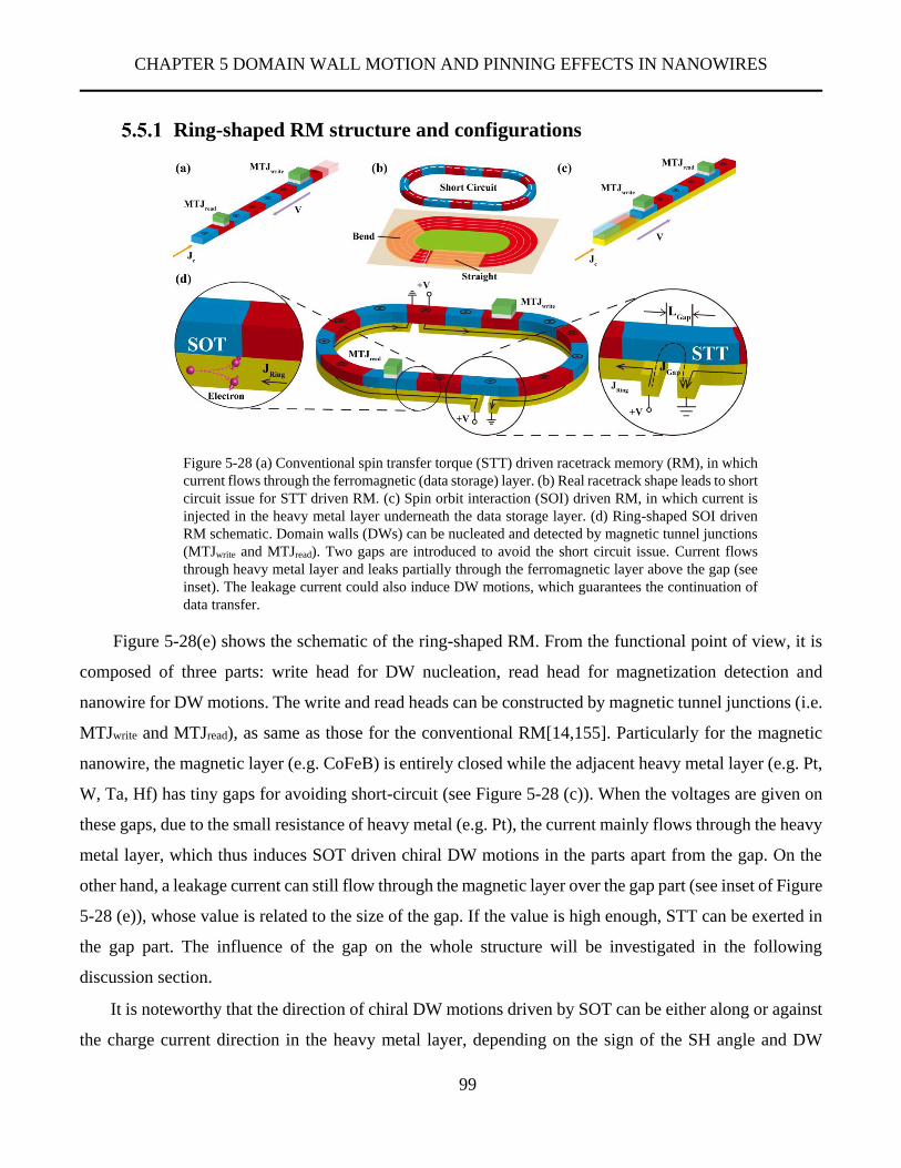
CHAPTER 5 DOMAIN WALL MOTION AND PINNING EFFECTS IN NANOWIRES
99
Ring-shaped RM structure and configurations
Figure 5-28(e) shows the schematic of the ring-shaped RM. From the functional point of view, it is
composed of three parts: write head for DW nucleation, read head for magnetization detection and
nanowire for DW motions. The write and read heads can be constructed by magnetic tunnel junctions (i.e.
MTJwrite and MTJread), as same as those for the conventional RM[14,155]. Particularly for the magnetic
nanowire, the magnetic layer (e.g. CoFeB) is entirely closed while the adjacent heavy metal layer (e.g. Pt,
W, Ta, Hf) has tiny gaps for avoiding short-circuit (see Figure 5-28 (c)). When the voltages are given on
these gaps, due to the small resistance of heavy metal (e.g. Pt), the current mainly flows through the heavy
metal layer, which thus induces SOT driven chiral DW motions in the parts apart from the gap. On the
other hand, a leakage current can still flow through the magnetic layer over the gap part (see inset of Figure
5-28 (e)), whose value is related to the size of the gap. If the value is high enough, STT can be exerted in
the gap part. The influence of the gap on the whole structure will be investigated in the following
discussion section.
It is noteworthy that the direction of chiral DW motions driven by SOT can be either along or against
the charge current direction in the heavy metal layer, depending on the sign of the SH angle and DW
Figure 5-28 (a) Conventional spin transfer torque (STT) driven racetrack memory (RM), in which
current flows through the ferromagnetic (data storage) layer. (b) Real racetrack shape leads to short
circuit issue for STT driven RM. (c) Spin orbit interaction (SOI) driven RM, in which current is
injected in the heavy metal layer underneath the data storage layer. (d) Ring-shaped SOI driven
RM schematic. Domain walls (DWs) can be nucleated and detected by magnetic tunnel junctions
(MTJwrite and MTJread). Two gaps are introduced to avoid the short circuit issue. Current flows
through heavy metal layer and leaks partially through the ferromagnetic layer above the gap (see
inset). The leakage current could also induce DW motions, which guarantees the continuation of
data transfer.

CHAPTER 5 DOMAIN WALL MOTION AND PINNING EFFECTS IN NANOWIRES
100
chirality of given multilayer system[78]. As the direction of STT driven DW motions is always against
the current direction, we choose Pt/CoFeB/MgO as the material configuration in order to shift the data
circularly and continuously in the ring structure. In addition, Pt has a relatively low resistivity among these
heavy metals, which is also much lower than that of ferromagnetic materials, such as CoFeB. Although
recent progress show that β-phase Ta and W can provide higher SH angle[78], their high resistivity are
unfavorable to the ring-shaped design.
Micromagnetic simulations
The functionality of the device proposed is investigated via micromagnetic simulations with Mumax
by introducing SOT and DMI into the Landau Lifshitz Gilbert (LLG) equation [152], as presented in
section 2.4 . In the gap part without sub heavy metal layer, the adiabatic and no adiabatic STT is introduced.
The following parameters were used in the simulation: the Gilbert damping constant is 0.015, the
non-adiabatic constant is 0.2, the spin Hall angle is 0.01, the Exchange stiffness is 20 pJ/m2, the spin
polarization rate is 0.5, the saturation magnetization is 1 MA/m, the uniaxial anisotropy is 800 kJ/m3, the
ferromagnetic layer thickness is 1 nm, the DMI parameter is 1.5 mJ/m2.
Results
From the point of view of DW trajectory, the ring-shaped RM can be divided into two parts: the
“Straight” and the “Bend”. Firstly, Figure 5-29 (a-d) demonstrates the chiral DW motions in the “Straight”:
a 40-nm-wide 1.28-um-long nanowire of Pt(2 nm)/CoFeB(0.6 nm)/MgO. DW motion velocity can reach
400 m/s with a current of 11101 A/m2. The motion velocity increases with the magnitude of injected
current and approaches the saturation when the current exceeds 11103 A/m2. Secondly, Figure 5-29 (e-
h) shows chiral DW motions in the “Bend”. The geometry of magnetic layer is designed to be a circle
whose external diameter is 1.024 um, width is 40 nm. The gap length of the heavy metal layer is fixed to
100 nm. The material parameters are the same as the “Straight” above. JGap and JRing are the current
densities through the gap and ring parts which are 12104.1 A/m2 and
11103 A/m2. With the drive of

CHAPTER 5 DOMAIN WALL MOTION AND PINNING EFFECTS IN NANOWIRES
101
the STT on the gap part and the drive of the SOT on the other part, DWs move along the ring
synchronously.
Compared with the circular structure, the racetrack-shaped structure, combining the “Straight” and
the “Bend” as shown in Figure 5-28 (b), promises the benefit in term of storage density. Figure 5-30 shows
the complete process of chiral DW motions in a really racetrack-shaped 16-bit RM. JGap and JRing are
12105 A/m2 and 12101 A/m2 respectively, which are larger than those in Figure 5-29, aiming to
overcome the pinning force from the pinning sites. The length of the gap is 100 nm each. From the results,
Figure 5-29 The top-view of the SOI driven chiral DW motions in the “Straight” and “Bend”. Red represents +z
magnetization, blue represents –z magnetization. (a-d) The “Straight”: 40 nm-wide and 1.28 um-long Pt(2
nm)/CoFeB(0.6 nm)/MgO. DW motion velocity can reach 400 m/s with a current of 5×10¹¹ A/m2. DW tilting
occurs which agrees with experimental results. (e-h) The “Bend”: external diameter Dext is 1024 nm, width d is
40 nm. The gap length of the heavy metal layer Lgap is 100 nm. Current injected into the heavy metal layer for
SOI part JRing is 3×10¹¹ A/m2 and leakage current in the gap part inducing STT JGap is 1.4×10¹² A/m2. The
different directions of current for these two parts guarantee the uni-direction of DW motions.

CHAPTER 5 DOMAIN WALL MOTION AND PINNING EFFECTS IN NANOWIRES
102
due to the DW motion inertia, the DWs can move synchronously and fluently with a 0.6-ns current pulse.
Here, adding the pinning sites is an important mean to optimize the controllability of DW shifting. Note
that the DMI stabilized SOT induced DWs are tilted and the tilting directions of the neighboring DWs
alternate[79]. This requires that the pinning sites should be symmetry on both sides of the racetrack in
order to make the equal effect on DWs with different tilting directions.
Discussions
To guarantee the functionality of the ring-shaped RM, one of the most critical conditions is that the
velocity of DW motions should be harmonious, which means DWs in ring part and gap part should at least
Figure 5-30 16-bit Racetrack-shaped RM schematic. Two gaps and symmetric pinning sites ( see
inset) are used for ensuring the functionality and stability of the RM. JGap and JRing are
A/m2 and A/m2. The length of gap is 100 nm each. 0.6 ns current pulses are sufficient
for DW motions due to the inertia.

CHAPTER 5 DOMAIN WALL MOTION AND PINNING EFFECTS IN NANOWIRES
103
move with comparative speeds. First, both the velocity of the SOT driven DW motion in the ring part and
the STT driven DW motion in the gap part depend on the current density in the heavy metal layer or in
the FM layer. These current densities have the following relationship,
𝐽𝑅𝑖𝑛𝑔𝜌𝑅𝑖𝑛𝑔𝐿𝑅𝑖𝑛𝑔 = 𝐽𝐺𝑎𝑝𝜌𝐺𝑎𝑝𝐿𝐺𝑎𝑝 (5-15)
where Ring and Gap are the resistivity of the heavy metal layer and the FM layer, 𝐿𝑅𝑖𝑛𝑔 and 𝐿𝐺𝑎𝑝 are
the lengths of the ring (without gap) and the gap. Therefore, the current density in the ring part and gap
part can be adjusted by the length ratio between 𝐿𝑅𝑖𝑛𝑔 and 𝐿𝐺𝑎𝑝. Because of the relatively shorter distance
of the gap, the current density in the FM of the gap part can be very large, thus promise a fast DW velocity.
Still, one should mind that the current in the gap part should not excess destructing density. According to
experimental observations, the STT driven DW velocity can reach only about a hundred meters per second
[55]. This velocity is still not able to match with the SOT driven DW velocity, which can reaches several
hundred meter per second [70,71]. In order to solve this mismatch of velocities, we can set a shorter
distance for the storage unit covering the gap part. For example, in the 16-bit RM shown in Figure 5-30,
a storage unit is defined by the section of nanowire between two notches. The length of the storage unit
covering the gap is only 100nm while a storage unit in the other part is about 150 nm. The DW can pass
the unit with gap and shift to the next notch with approximately the same time as others. In addition, in
the simulations that we performed, we didn’t observe a very large decrease of DW velocity in the gap part
as expected. This can be explained by the inertia of the DW[156,157]. The roughness is neglected in our
simulations and the ferromagnetic material that we applied, CoFeB, has a relatively small damping
constant. This allows the DWs to continue moving over a distance by a force of inertia[156,157].
Compared to conventional stripe-shaped structure, this ring-shaped structure can keep all the data
during the shifting process, without increasing overhead and requiring additional manipulations. We
believe this ring-shaped RM will vitalize the development and practical application of RM[158].
Conclusion
In this chapter, the DW motion in the nanowire driven by the magnetic field or by the combined effect
of the field and electrical current was experimentally studied. The polarization ratio of CoFeB in the
Ta/CoFeB/MgO structure has been extracted based on the contribution of STT on the DW motion velocity
and was found to be as low as 26%, much lower than the value measured through the Point-Contact
Andreev Reflection (65%)[151] or through the superconducting tunneling spectroscopy (53%)[91–93] in
CHAPTER 5 DOMAIN WALL MOTION AND PINNING EFFECTS IN NANOWIRES
104
the heavy metal/CoFeB/Oxide layer structure. This low polarization ratio may be caused by the injection
of SH current or the diffusion of electrons from the Ta layer.
The DW pinning effects in the nanowire and the dependence of the depinning field on the width of
wire was measured and analyzed. The enhancement of pinning effects when a current was applied was
observed and a possible explanation is an effect of the SH current. At last, a ring-shaped RM, which can
avoid the data overflow, was proposed and verified with micromagnetic simulations.

CHAPTER 6 GENERAL CONCLUSIONS AND PERSPECTIVES
105
Chapter 6 General conclusions and perspectives
This thesis is devoted to the study of magnetic DW properties and dynamics in Ta/Co40Fe40B20/MgO
thin films and nanowires with PMA. The observation of domain structures and DW dynamics relied
mainly on Kerr microscopy. In order to study the DW behavior in the nanostructures, very short magnetic
pulses of high amplitude were required. We could reach this aim by creating small coils of very low
inductance and by connecting them to a high current pulse generator. We have succeeded to create
microsecond magnetic pulses, with a rise time shorter than 200 ns. Electric current pulses have been
applied on the nanowires and we were able to create the synchronized magnetic field pulse and electric
current pulse with a duration of several microseconds.
Thanks to the high-resolution Kerr microscope and the proper magnetic field pulse produced by the
mini coil, we have conducted a series of experiments related to the DW surface tension. We studied the
dynamic of DW in the nanowires, including the DW pinning effects and the DW motion driven by a
magnetic field or current, or by their combined effects.
The main contributions of this thesis are:
DWs surface tension was directly observed using a Kerr microscope and DWs surface energy
was directly quantified. In zero external field, the spontaneous collapse of semicircular
domain bubble was observed. This phenomenon was explained with the concept of the
Laplace pressure due to the DW surface energy. The DW surface energy was quantified by
measuring the external field required to stabilize the domain bubble.
The origin of the DW pinning effects in some artificial structures, such as Hall crosses or the
entrance from nanowire to the nucleation pad, were explained using the concept of DWs
surface tension. The linear dependence of the DW depinning field in these structures on the
width of wire was used to quantify the DW surface energy.
A new type of magnetic sensor based on the elasticity of DWs has been designed and verified
using micromagnetic simulations.
The DW pinning effects in CoFeB nanowires was characterized. A linear dependence of the
depinning field of the strong pinning sites on the width of wire was observed and analyzed. It
points to an extrinsic nature of these strong pinning points, which would be on the edges of
the nanowires and due to the nanopatterning.

CHAPTER 6 GENERAL CONCLUSIONS AND PERSPECTIVES
106
Velocities of the field-driven and the current-driven DW motion in heavy metal/CoFeB/MgO
nanowires was measured. We have found experimentally that the velocity of the DW motion
driven by the combined effect of the field and the current equals to the sum of the velocity
contributed by these two forces separately. The spin polarization of CoFeB was extracted and
was found equal to 26%. A possible explanation for this low spin polarization of CoFeB is an
injection of differently polarized spin from Ta to CoFeB due to the spin Hall effect. The
diffusion of electrons between the CoFeB and Ta layer, which has a strong SOC, may also be
a reason for this low spin polarization.
We found that the DW depinning field in nanowires increased significantly when a current
was applied simultaneously, irrespective of the relative DW motion direction and the current
direction. We think this could arise from spin Hall current coming from the Ta layer. Using
micromagnetic simulations, we show that the intrinsic DW pinning effects in magnetic wires
can be enhanced by the SH current. However, only the extrinsic pinning effects in one of the
two edges can be enhanced.
A ring-shaped racetrack memory device based on the combined works of the STT and SOT
driven DW motion in nanowires was designed and verified using micromagnetic simulations.
This racetrack memory can avoid the data drop out compared with traditional line-shaped
racetrack memory.
Our results have brought some interesting results and have explained several phenomena. We have
found new ways, which could be used to answer some still opened questions. Furthermore, our work has
also risen several new questions:
1. We have developed two methods to measure the DW surface energy γDW. These methods may be
useful to quantify the intrinsic parameter of material, such as the DMI constant, the exchange stiffness.
Among the various methods to quantify the strength of DMI with Kerr microscope, e.g. by probing
the asymmetric propagation of circular DW in creep regime when an in-plane field is present[5], or by
observing the in-plane field that changes the direction of the spin Hall current-induced DW motion[159],
only the effective DMI field HDM can be obtained. We have[160],
D = 𝜇0𝐻𝐷𝑀𝑀𝑆√𝐴𝑒𝑥
𝐾𝑒𝑓𝑓 (6-1)
CHAPTER 6 GENERAL CONCLUSIONS AND PERSPECTIVES
107
It is difficult to access directly to the intrinsic parameter D, since the exchange stiffness Aex is difficult
to be quantified with Kerr microscope.
In fact, the quantification of Aex in ultra-thin films is always a difficult issue. The commonly used
methods to measure Aex are mainly based on the spin wave frequency and dispersion[125] (e.g. using
Brillouin light scattering (BSL)[161–163], spin-polarized electron energy loss spectroscopy,
ferromagnetic resonance (FMR)[139,164]). However, for ultrathin films less than 10 nm, the above
methods become less useful because they are not sufficiently sensitive to detect spin waves[165].
Moreover, it was found that the value of A in the ultra-thin film is different than that in bulk material
(thickness larger than ~10nm) due to the interfacial effect. The value of Aex obtained in bulk material
cannot be used in ultrathin film[165].
Now, Aex can be extracted once the DW surface energy γDW is accurately quantified, since γ𝐷𝑊 =
4√𝐴𝑒𝑥𝐾𝑒𝑓𝑓 in film without DMI.
Furthermore, if DMIs exist, the DW surface energy changes[166],
γ𝐷𝑊 = 4√𝐴𝑒𝑥𝐾𝑒𝑓𝑓 − πD (6-2)
Once the DW surface energy γ𝐷𝑊 is obtained with our methods, we can deduce directly the value of
D from Eq.(6-1) & (6-2),
D =
γ𝐷𝑊4𝐾𝑒𝑓𝑓
𝜇0𝐻𝐷𝑀𝑀𝑆−𝜋 (6-3)
and,
𝐴𝑒𝑥 =𝐾𝑒𝑓𝑓 𝛾𝐷𝑊
2
(4𝐾𝑒𝑓𝑓−𝜋𝜇0𝐻𝐷𝑀𝑀𝑆)2 (6-4)
From Eq. (6-3), the expected uncertainty of the extracted D is in the same order than γDW, assuming
that other parameters such as Keff, HDM, and MS are well quantified.
This method needs to be explored in the future studies.
2. We have experimentally observed the enhancement of the DW pinning effect in Ta/CoFeB narrow
wire when a current is applied. With micromagnetic simulation, we show that a spin Hall current injected
into the magnetic layer can result in this enhancement. However, further experiments are needed to study
this effect more clearly. For example, one can etch some regular notches in the edge of wires to observe
the change of the profile of the DW when a current was applied because a DW tilting is predicted by the

CHAPTER 6 GENERAL CONCLUSIONS AND PERSPECTIVES
108
simulation in this case. The wire can be enlarged (e.g. to more than 10 μm) so that the DW behavior can
be observed clearly, because, with the Kerr microscope, we were not able to clearly observe the shape of
the DW in the 1.5 μm wire studied. The simulation has predicted a variation of DW tilting angle as a
function of applied current density, through which the SH angle may be extracted. Further experiments
can be conducted to explore this method.
3. We have found that in the Ta/CoFeB/MgO narrow wire, when the applied easy-axis field is weak
or zero, the DW is very difficult to be moved by the current. When the current increased to a critical value,
the DW motion direction becomes stochastic. This phenomenon has not been completely understood.
Further studies are needed to understand this question.
4. We have observed the DW motion driven by the synchronized current and the magnetic field
applied along the easy axis and explained the DW velocity by the combined effects of the field and STT.
However, in the heavy metal/magnetic layer/MgO structure, the SH current from the heavy metal layer
begins to work when an in-plane field is applied. It might be interesting to implement an in-plane field in
addition to the present system and study the combined effect of the magnetic field, the STT and the SOT
on the DW motion. Some important parameters such as the SH angle, the non-adiabatic constant might be
-6 -4 -2 0 2 4 6
x 1011
-150
-100
-50
0
50
100
150
Jc (A/m2)
DW
ve
locity (
m/s
)
Hx=0
Hx=-10mT
Hx=+10mT
Hx=+20mT
-0.05 -0.03 -0.01 0.01 0.03 0.05-300
-200
-100
0
100
200
300
Hx (T)
DW
ve
locity (
m/s
)
jc=-6*10
11A/m
2
jc=-3*10
11A/m
2
jc=-1*10
11A/m
2
jc=1*10
11A/m
2
jc=3*10
11A/m
2
jc=6*10
11A/m
2
Figure 6-1The DW motion velocity predicted by the 1D model. Parameters: No field was applied along the
z-axis (easy axis), DW width: 10 nm, shape anisotropy field Hk: 105 A/m; both the adiabatic STT, non-
adiabatic STT from the in-plane current in FM layer, and the SOT caused by the injection of the SH current
are considered. Non adiabatic constant β=0.1; the polarization P=0.26 for in-plane current. The spin Hall
angle is supposed to be ΘSH=-0.05. An in-plane field along the longitudinal direction (x-axis, DW motion
direction) was applied. (a) DW motion velocities vs. current density. (b) DW velocities vs. the in plane
field.
(a) (b)
0

CHAPTER 6 GENERAL CONCLUSIONS AND PERSPECTIVES
109
properly extracted based on these experiments. Based on the numerical calculation of 1D model, we found
that the DW motion induced by the combined effect of the STT and SOT is linear as a function of the
magnitude of the in-plane field, as shown in Figure 6-1 (b). The vertical intercept represents the
contribution from the STT and the slope represents the contribution from the SOT. If this relationship
could be experimentally measured, the spin Hall angle could be extracted by linearly fitting the
experimental results with the 1D model.
In addition, we found that the horizontal intercept changes with the non-adiabatic constant ξ, as
shown in Figure 6-2. Because both the SOT and non-adiabatic STT enters the 1D model in the form
effective fields. The change of the horizontal intercept with β is the result of the competition between this
two terms. By locating this intercept, the non-adiabatic constant might be extracted.
5. Through numerical calculations based on the 1D model, we have found that the damping like SOT
due to the injection of the SH current tends to stabilize the magnetization of DW in the polarizing direction
of the SH current. Consequently, the arrival of the precessional mode will be delayed, i.e., the Walker
breakdown field increase, as shown in Figure 6-3. It should be interesting if this prediction could be
experimentally observed. To reach this aim, one should find a material/structure with a relatively large
-10 -8 -6 -4 -2 0 2 4 6 8 10-100
0
100
-10 -8 -6 -4 -2 0 2 4 6 8 10-100
0
100
-10 -8 -6 -4 -2 0 2 4 6 8 10-100
0
100
-10 -8 -6 -4 -2 0 2 4 6 8 10-100
0
100
Hx (mT)
DW
vel
oci
ty (
m/s
)
ξ=0
ξ =0.05
ξ =0.1
ξ =0.2
Figure 6-2 Numerically calculated DW motion velocities based on the 1D model. Non-adiabatic constant
ξ changes from 0 to 0.2. Other parameters are same as that in Fig. 6-1
-10 -8 -6 -4 -2 0 2 4 6 8 10-100
0
100
jc=-6*1011A/m2
jc=-1*1011A/m2
jc=1*1011A/m2
jc=6*1011A/m2
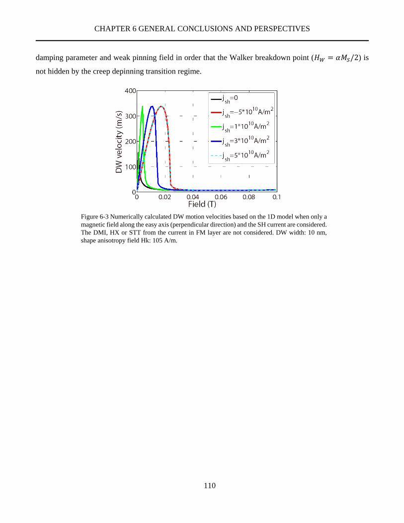
CHAPTER 6 GENERAL CONCLUSIONS AND PERSPECTIVES
110
damping parameter and weak pinning field in order that the Walker breakdown point (𝐻𝑊 = 𝛼𝑀𝑆/2) is
not hidden by the creep depinning transition regime.
Figure 6-3 Numerically calculated DW motion velocities based on the 1D model when only a
magnetic field along the easy axis (perpendicular direction) and the SH current are considered.
The DMI, HX or STT from the current in FM layer are not considered. DW width: 10 nm,
shape anisotropy field Hk: 105 A/m.

REFERENCES
111
References
1. Vernier, N.; Adam, J. P.; Eimer, S.; Agnus, G.; Devolder, T.; Hauet, T.; Ocker, B.; Garcia, F.;
Ravelosona, D. Measurement of magnetization using domain compressibility in CoFeB films with
perpendicular anisotropy. Appl. Phys. Lett. 2014, 104, 122404, doi:10.1063/1.4869482.
2. Yamanouchi, M.; Jander, A.; Dhagat, P.; Ikeda, S.; Matsukura, F.; Ohno, H. Domain Structure in
CoFeB Thin Films With Perpendicular Magnetic Anisotropy. IEEE Magn. Lett. 2011, 2, 3000304,
doi:10.1109/LMAG.2011.2159484.
3. Haghgoo, S.; Cubukcu, M.; Von Bardeleben, H. J.; Thevenard, L.; Lemaître, A.; Gourdon, C.
Exchange constant and domain wall width in (Ga,Mn)(As,P) films with self-organization of
magnetic domains. Phys. Rev. B 2010, 82, 041301, doi:10.1103/PhysRevB.82.041301.
4. Buford, B.; Dhagat, P.; Jander, A. Estimating exchange stiffness of thin films with perpendicular
anisotropy using magnetic domain images. IEEE Magn. Lett. 2016, 7, 1–5,
doi:10.1109/LMAG.2016.2611681.
5. Je, S.-G.; Kim, D.-H.; Yoo, S.-C.; Min, B.-C.; Lee, K.-J.; Choe, S.-B. Asymmetric magnetic
domain-wall motion by the Dzyaloshinskii-Moriya interaction. Phys. Rev. B 2013, 88, 214401,
doi:10.1103/PhysRevB.88.214401.
6. Currivan-Incorvia, J. A.; Siddiqui, S.; Dutta, S.; Evarts, E. R.; Zhang, J.; Bono, D.; Ross, C. A.;
Baldo, M. A. Logic circuit prototypes for three-terminal magnetic tunnel junctions with mobile
domain walls. Nat. Commun. 2016, 7, 10275, doi:10.1038/ncomms10275.
7. Allwood, D. A.; Xiong, G.; Faulkner, C. C.; ATKINSON, D.; Petit, D.; Cowburn, R. P. Magnetic
Domain-Wall Logic. Science 2005, 309, 1688–1692, doi:10.1126/science.1108813.
8. Sengupta, A.; Shim, Y.; Roy, K. Proposal for an all-spin artificial neural network: Emulating neural
and synaptic functionalities through domain wall motion in ferromagnets. IEEE Trans. Biomed.
Circuits Syst. 2016, 10, 1152–1160, doi:10.1109/TBCAS.2016.2525823.
9. Sharad, M.; Augustine, C.; Panagopoulos, G.; Roy, K. Spin-based neuron model with domain-wall
magnets as synapse. IEEE Trans. Nanotechnol. 2012, 11, 843–853,
doi:10.1109/TNANO.2012.2202125.
10. Fan, D.; Shim, Y.; Raghunathan, A.; Roy, K. STT-SNN: A Spin-Transfer-Torque Based Soft-
Limiting Non-Linear Neuron for Low-Power Artificial Neural Networks. IEEE Trans. Nanotechnol.
2015, 14, 1013–1023, doi:10.1109/TNANO.2015.2437902.

REFERENCES
112
11. Wagner, K.; Kákay, A.; Schultheiss, K.; Henschke, A.; Sebastian, T.; Schultheiss, H. Magnetic
domain walls as reconfigurable spin-wave nanochannels. Nat. Nanotechnol. 2016, 11, 432–436,
doi:10.1038/nnano.2015.339.
12. Parkin, S.; Yang, S.-H. Memory on the racetrack. Nat. Nanotechnol. 2015, 10, 195–198,
doi:10.1038/nnano.2015.41.
13. Parkin, S. S. P.; Hayashi, M.; Thomas, L. Magnetic domain-wall racetrack memory. Science 2008,
320, 190–194, doi:10.1126/science.1145799.
14. Ikeda, S.; Miura, K.; Yamamoto, H.; Mizunuma, K.; Gan, H. D.; Endo, M.; Kanai, S.; Hayakawa,
J.; Matsukura, F.; Ohno, H. A perpendicular-anisotropy CoFeB-MgO magnetic tunnel junction. Nat.
Mater. 2010, 9, 721–724, doi:10.1038/nmat2804.
15. Wells, J.; Krzysteczko, P.; Caprile, A.; Gribkov, B.; Schumacher, H. W.; Lee, J. H.; Cowburn, R.;
Kazakova, O. Magnetic Particle Nanosensing by Nucleation of Domain Walls in Ultra-Thin
CoFeB/Pt Devices. IEEE Trans. Magn. 2016, 52, doi:10.1109/TMAG.2016.2524074.
16. Ikeda, S.; Hayakawa, J.; Ashizawa, Y.; Lee, Y. M.; Miura, K.; Hasegawa, H.; Tsunoda, M.;
Matsukura, F.; Ohno, H. Tunnel magnetoresistance of 604% at 300 K by suppression of Ta
diffusion in CoFeBMgOCoFeB pseudo-spin-valves annealed at high temperature. Appl. Phys. Lett.
2008, 93, 2006–2009, doi:10.1063/1.2976435.
17. Jang, Y.; Nam, C.; Kim, J. Y.; Cho, B. K.; Cho, Y. J.; Kim, T. W. Magnetic field sensing scheme
using CoFeB/MgO/CoFeB tunneling junction with superparamagnetic CoFeB layer. Appl. Phys.
Lett. 2006, 89, 163119, doi:10.1063/1.2370876.
18. Zhang, Y.; Zhao, W. S.; Ravelosona, D.; Klein, J. O.; Kim, J. V.; Chappert, C. Perpendicular-
magnetic-anisotropy CoFeB racetrack memory. J. Appl. Phys. 2012, 111, 2010–2015,
doi:10.1063/1.4716460.
19. Stöhr, J.; Siegmann, H. C. Magnetism:FromFundamentals to Nanoscale Dynamics; Springer Berlin
Heidelberg: Berlin, Heidelberg, 2006; ISBN 978-3-540-30282-7.
20. Babujian, H. M. Exact solution of the isotropic Heisenberg chain with arbitrary spins:
Thermodynamics of the model. Nucl. Physics, Sect. B 1983, 215, 317–336, doi:10.1016/0550-
3213(83)90668-5.
21. Hubert, A.; Schäfer, R. Magnetic Domains,The Analysis of Magnetic Microstructures; 3rd ed.;
Springer: New York, 1998; ISBN 978-3-540-85054-0.
REFERENCES
113
22. Zhang, B.; Cao, A.; Qiao, J.; Tang, M.; Cao, K.; Zhao, X.; Eimer, S.; Si, Z.; Lei, N.; Wang, Z.; Lin,
X.; Zhang, Z.; Wu, M.; Zhao, W. Influence of heavy metal materials on magnetic properties of
Pt/Co/heavy metal tri-layered structures. Appl. Phys. Lett. 2017, 110, doi:10.1063/1.4973477.
23. Thiaville, A.; Rohart, S.; Jué, É.; Cros, V.; Fert, A. Dynamics of Dzyaloshinskii domain walls in
ultrathin magnetic films. EPL (Europhysics Lett.) 2012, 100, 57002, doi:10.1209/0295-
5075/100/57002.
24. Tetienne, J.-P.; Hingant, T.; Martínez, L. J.; Rohart, S.; Thiaville, A.; Diez, L. H.; Garcia, K.; Adam,
J.-P.; Kim, J.-V.; Roch, J.-F.; Miron, I. M.; Gaudin, G.; Vila, L.; Ocker, B.; Ravelosona, D.; Jacques,
V. The nature of domain walls in ultrathin ferromagnets revealed by scanning nanomagnetometry.
Nat. Commun. 2015, 6, 6733, doi:10.1038/ncomms7733.
25. Nakatani, Y.; Thiaville, A.; Miltat, J. Head-to-head domain walls in soft nano-strips: A refined
phase diagram. J. Magn. Magn. Mater. 2005, 290–291 PA, 750–753,
doi:10.1016/j.jmmm.2004.11.355.
26. Kaplan, B.; Gehring, G. A. The domain structure in ultrathin magnetic films. J. Mag. Mag. Mat.
1993, 128, 111–116, doi:10.1016/0304-8853(93)90863-W.
27. Nguyen, V. D.; Vila, L.; Marty, A.; Pillet, J. C.; Notin, L.; Beigné, C.; Pizzini, S.; Attané, J. P.
Dimensionality effects on the magnetization reversal in narrow FePt nanowires. Appl. Phys. Lett.
2012, 100, doi:10.1063/1.4721672.
28. Ryu, J.; Choe, S. B.; Lee, H. W. Magnetic domain-wall motion in a nanowire: Depinning and creep.
Phys. Rev. B 2011, 84, 1–12, doi:10.1103/PhysRevB.84.075469.
29. Cayssol, F.; Ravelosona, D.; Chappert, C.; Ferré, J.; Jamet, J. P. Domain Wall Creep in Magnetic
Wires. Phys. Rev. Lett. 2004, 92, 107202–1, doi:10.1103/PhysRevLett.92.107202.
30. Schellekens, a. J.; van den Brink, a.; Franken, J. H.; Swagten, H. J. M.; Koopmans, B. Electric-
field control of domain wall motion in perpendicularly magnetized materials. Nat. Commun. 2012,
3, 847, doi:10.1038/ncomms1848.
31. Franke, K. J. A.; Van de Wiele, B.; Shirahata, Y.; Hämäläinen, S. J.; Taniyama, T.; van Dijken, S.
Reversible electric-field-driven magnetic domain-wall motion. Phys. Rev. X 2015, 5, 1–9,
doi:10.1103/PhysRevX.5.011010.
32. Franken, J. H.; Swagten, H. J. M.; Koopmans, B. Shift registers based on magnetic domain wall
ratchets with perpendicular anisotropy. Nat. Nanotechnol. 2012, 7, 499–503,
REFERENCES
114
doi:10.1038/nnano.2012.111.
33. Zhu, J.; Han, Z.; Su, Y.; Hu, J. Energy-imbalance mechanism of domain wall motion induced by
propagation spin waves in finite magnetic nanostripe. J. Magn. Magn. Mater. 2014, 369, 96–100,
doi:10.1016/j.jmmm.2014.06.015.
34. Wang, X. G.; Guo, G. H.; Nie, Y. Z.; Wang, D. W.; Zeng, Z. M.; Li, Z. X.; Tang, W. Microwave-
assisted domain-wall motion induced by alternating spin-polarized current. Phys. Rev. B 2014, 89,
2–7, doi:10.1103/PhysRevB.89.144418.
35. Kim, J.-S.; Stärk, M.; Kläui, M.; Yoon, J.; You, C.-Y.; Lopez-Diaz, L.; Martinez, E. Interaction
between propagating spin waves and domain walls on a ferromagnetic nanowire. Phys. Rev. B 2012,
85, 174428, doi:10.1103/PhysRevB.85.174428.
36. Tatara, G.; Kohno, H. Theory of Current-Driven Domain Wall Motion: Spin Transfer versus
Momentum Transfer. Phys. Rev. Lett. 2004, 92, 086601, doi:10.1103/PhysRevLett.92.086601.
37. Kläui, M.; Jubert, P.-O.; Allenspach, R.; Bischof, A.; Bland, J. A. C.; Faini, G.; Rüdiger, U.; Vaz,
C. A. F.; Vila, L.; Vouille, C. Direct observation of domain-wall congurations transformed by spin
currents. Phys. Rev. Lett. 2005, 95, 26601.
38. Rubio-Marcos, F.; Campo, A. Del; Marchet, P.; Fernández, J. F. Ferroelectric domain wall motion
induced by polarized light. Nat. Commun. 2015, 6, doi:10.1038/ncomms7594.
39. Schlickeiser, F.; Ritzmann, U.; Hinzke, D.; Nowak, U. Role of entropy in domain wall motion in
thermal gradients. Phys. Rev. Lett. 2014, 113, 1–5, doi:10.1103/PhysRevLett.113.097201.
40. Metaxas, P. J.; Jamet, J. P.; Mougin, A.; Cormier, M.; Ferré, J.; Baltz, V.; Rodmacq, B.; Dieny, B.;
Stamps, R. L. Creep and flow regimes of magnetic domain-wall motion in ultrathin Pt/Co/Pt films
with perpendicular anisotropy. Phys. Rev. Lett. 2007, 99, 217208,
doi:10.1103/PhysRevLett.99.217208.
41. Cormier, M.; Mougin, A.; Adam, J.; Metaxas, P.; Ferré, J. Domain wall dynamics in ultrathin films:
Size and thickness influence- Application to perpendicularly magnetized films; Orsay, 2006;
42. Mougin, A.; Cormier, M.; Adam, J. P.; Metaxas, P. J.; Ferré, J. Domain wall mobility, stability and
Walker breakdown in magnetic nanowires. Europhys. Lett. 2007, 78, 57007, doi:10.1209/0295-
5075/78/57007.
43. Infante, G.; Varga, R.; Badini-Confalonieri, G. A.; Vázquez, M. Locally induced domain wall
damping in a thin magnetic wire. Appl. Phys. Lett. 2009, 95, 1–4, doi:10.1063/1.3174919.

REFERENCES
115
44. Weindler, T.; Bauer, H. G.; Islinger, R.; Boehm, B.; Chauleau, J. Y.; Back, C. H. Magnetic damping:
Domain wall dynamics versus local ferromagnetic resonance. Phys. Rev. Lett. 2014, 113, 1–5,
doi:10.1103/PhysRevLett.113.237204.
45. Glathe, S.; Mattheis, R.; Berkov, D. V. Direct observation and control of the Walker breakdown
process during a field driven domain wall motion. Appl. Phys. Lett. 2008, 93, 1–4,
doi:10.1063/1.2975181.
46. Thiaville, A.; García, J. M.; Miltat, J. Domain wall dynamics in nanowires. J. Magn. Magn. Mater.
2002, 242–245, 1061–1063, doi:10.1016/S0304-8853(01)01353-1.
47. Attané, J. P.; Ravelosona, D.; Marty, A.; Nguyen, V. D.; Vila, L. Coercivity enhancement in FePt
nanowires due to the suppression of available paths for domain wall propagation. Phys. Rev. B 2011,
84, 1–6, doi:10.1103/PhysRevB.84.144418.
48. Chen, T. Y.; Erickson, M. J.; Crowell, P. A.; Leighton, C. Surface roughness dominated pinning
mechanism of magnetic vortices in soft ferromagnetic films. Phys. Rev. Lett. 2012, 109, 1–5,
doi:10.1103/PhysRevLett.109.097202.
49. Attané, J. P.; Ravelosona, D.; Marty, A.; Samson, Y.; Chappert, C. Thermally activated depinning
of a narrow domain wall from a single defect. Phys. Rev. Lett. 2006, 96, 1–4,
doi:10.1103/PhysRevLett.96.147204.
50. Lemerle, S.; Ferré, J.; Chappert, C.; Mathet, V.; Giamarchi, T.; Le Doussal, P. Domain Wall Creep
in an Ising Ultrathin Magnetic Film. Phys. Rev. Lett. 1998, 80, 849–852,
doi:10.1103/PhysRevLett.80.849.
51. Diaz Pardo, R.; Savero Torres, W.; Kolton, A. B.; Bustingorry, S.; Jeudy, V. Universal depinning
transition of domain walls in ultrathin ferromagnets. Phys. Rev. B 2017, 95, 1–7,
doi:10.1103/PhysRevB.95.184434.
52. Ralph, D. C.; Stiles, M. D. Spin transfer torques. J. Magn. Magn. Mater. 2008, 320, 1190–1216,
doi:10.1016/j.jmmm.2007.12.019.
53. Slonczewski, J. C. Currents, torques, and polarization factors in magnetic tunnel junctions. Phys.
Rev. B 2005, 71, 1–10, doi:10.1103/PhysRevB.71.024411.
54. Slonczewski, J. C. Current-driven excitation of magnetic multilayers. J. Magn. Magn. Mater. 1996,
159, L1–L7, doi:10.1016/0304-8853(96)00062-5.
55. Yamanouchi, M.; Chiba, D.; Matsukura, F.; Ohno, H. Current-induced domain wall switching in a

REFERENCES
116
ferromagnetic semiconductor structure. Nature 2004, 428, 539–542, doi:10.1038/nature02425.1.
56. Berger, L. Domain drag effect in the presence of variable magnetic field or variable transport
current. J. Appl. Phys. 1979, 50, 2137–2139, doi:10.1063/1.327083.
57. Berger, L. Low-field magnetoresistance and domain drag in ferromagnets. J. Appl. Phys. 1978, 49,
2156–2161, doi:10.1063/1.324716.
58. Freitas, P. P.; Berger, L. Observation of s-d exchange force between domain walls and electric
current in very thin Permalloy films. J. Appl. Phys. 1985, 57, 1266–1269, doi:10.1063/1.334524.
59. Hung, C. Y.; Berger, L. Exchange forces between domain wall and electric current in permalloy
films of variable thickness. J. Appl. Phys. 1988, 63, 4276–4278, doi:10.1063/1.340201.
60. Li, Z.; Zhang, S. Domain-wall dynamics driven by adiabatic spin-transfer torques. Phys. Rev. B
2004, 70, 1–10, doi:10.1103/PhysRevB.70.024417.
61. Boulle, O.; Malinowski, G.; Klaui, M. Current-induced domain wall motion in nanoscale
ferromagnetic elements. Mater. Sci. Eng. R Reports 2011, 72, 159–187,
doi:10.1016/j.mser.2011.04.001.
62. Zhang, J.; Levy, P. M.; Zhang, S.; Antropov, V. Identification of transverse spin currents in
noncollinear magnetic structures. Phys. Rev. Lett. 2004, 93, 2–5,
doi:10.1103/PhysRevLett.93.256602.
63. Thiaville, A.; Nakatani, Y.; Miltat, J.; Suzuki, Y. Micromagnetic understanding of current-driven
domain wall motion in patterned nanowires. 2004, 990, doi:10.1209/epl/i2004-10452-6.
64. Hayashi, M.; Thomas, L.; Rettner, C.; Moriya, R.; Bazaliy, Y. B.; Parkin, S. S. P. Current driven
domain wall velocities exceeding the spin angular momentum transfer rate in permalloy nanowires.
Phys. Rev. Lett. 2007, 98, 1–4, doi:10.1103/PhysRevLett.98.037204.
65. Yamanouchi, M. Universality Classes for Domain Wall. Cell 2008, 1726, 1–5,
doi:10.1126/science.1145516.
66. DuttaGupta, S.; Fukami, S.; Zhang, C.; Sato, H.; Yamanouchi, M.; Matsukura, F.; Ohno, H.
Adiabatic spin-transfer-torque-induced domain wall creep in a magnetic metal. Nat. Phys. 2016, 12,
333–336, doi:10.1038/nphys3593.
67. Duine, R. A.; Smith, C. M. Creep of current-driven domain-wall lines: Effects of intrinsic versus
extrinsic pinning. Phys. Rev. B 2008, 77, 1–6, doi:10.1103/PhysRevB.77.094434.
68. Gambardella, P.; Miron, I. M. Current-induced spin-orbit torques. Philos. Trans. R. Soc. A Math.

REFERENCES
117
Phys. Eng. Sci. 2011, 369, 3175–3197, doi:10.1098/rsta.2010.0336.
69. Sinova, J.; Valenzuela, S. O.; Wunderlich, J.; Back, C. H.; Jungwirth, T. Spin Hall effects. Rev.
Mod. Phys. 2015, 87, 1213–1260, doi:10.1103/RevModPhys.87.1213.
70. Miron, I. M.; Moore, T.; Szambolics, H.; Buda-Prejbeanu, L. D.; Auffret, S.; Rodmacq, B.; Pizzini,
S.; Vogel, J.; Bonfim, M.; Schuhl, A.; Gaudin, G. Fast current-induced domain-wall motion
controlled by the Rashba effect. Nat. Mater. 2011, 10, 419–423, doi:10.1038/nmat3020.
71. Ryu, K.-S.; Thomas, L.; Yang, S.-H.; Parkin, S. Chiral spin torque at magnetic domain walls. Nat.
Nanotechnol. 2013, 8, 527–533, doi:10.1038/nnano.2013.102.
72. Emori, S.; Bauer, U.; Ahn, S.-M.; Martinez, E.; Beach, G. S. D. Current-driven dynamics of chiral
ferromagnetic domain walls. Nat. Mater. 2013, 12, 611–616, doi:10.1038/nmat3675.
73. Khvalkovskiy, A. V.; Cros, V.; Apalkov, D.; Nikitin, V.; Krounbi, M.; Zvezdin, K. A.; Anane, A.;
Grollier, J.; Fert, A. Matching domain-wall configuration and spin-orbit torques for efficient
domain-wall motion. Phys. Rev. B 2013, 87, 2–6, doi:10.1103/PhysRevB.87.020402.
74. Perez, N.; Martinez, E.; Torres, L.; Woo, S. H.; Emori, S.; Beach, G. S. D. Chiral magnetization
textures stabilized by the Dzyaloshinskii-Moriya interaction during spin-orbit torque switching.
Appl. Phys. Lett. 2014, 104, 092403, doi:10.1063/1.4867199.
75. Liu, L.; Pai, C.-F.; Li, Y.; Tseng, H. W.; Ralph, D. C.; Buhrman, R. A. Spin-Torque Switching with
the Giant Spin Hall Effect of Tantalum. Science 2012, 336, 555–558, doi:10.1126/science.1218197.
76. Haazen, P. P. J.; Murè, E.; Franken, J. H.; Lavrijsen, R.; Swagten, H. J. M.; Koopmans, B. Domain
wall depinning governed by the spin Hall effect. Nat. Mater. 2013, 12, 299–303,
doi:10.1038/nmat3553.
77. Ramu, M.; Goolaup, S.; Gan, W. L.; Krishnia, S.; Lim, G. J.; Lew, W. S. Spin orbit torque induced
asymmetric depinning of chiral Néel domain wall in Co/Ni heterostructures. Appl. Phys. Lett. 2017,
110, doi:10.1063/1.4980120.
78. Torrejon, J.; Kim, J.; Sinha, J.; Mitani, S.; Hayashi, M.; Yamanouchi, M.; Ohno, H. Interface
control of the magnetic chirality in CoFeB/MgO heterostructures with heavy-metal underlayers.
Nat. Commun. 2014, 5, 1–8, doi:10.1038/ncomms5655.
79. Boulle, O.; Rohart, S.; Buda-Prejbeanu, L. D.; Jué, E.; Miron, I. M.; Pizzini, S.; Vogel, J.; Gaudin,
G.; Thiaville, A. Domain Wall Tilting in the Presence of the Dzyaloshinskii-Moriya Interaction in
Out-of-Plane Magnetized Magnetic Nanotracks. Phys. Rev. Lett. 2013, 111, 217203,

REFERENCES
118
doi:10.1103/PhysRevLett.111.217203.
80. Ryu, K. S.; Thomas, L.; Yang, S. H.; Parkin, S. S. P. Current induced tilting of domain walls in
high velocity motion along perpendicularly magnetized micron-sized Co/Ni/Co racetracks. Appl.
Phys. Express 2012, 5, 1–3, doi:10.1143/APEX.5.093006.
81. Kim, K. W.; Lee, H. W. Thermal fluctuation field for current-induced domain wall motion. Phys.
Rev. B 2010, 82, 1–16, doi:10.1103/PhysRevB.82.134431.
82. Yang, S. H.; Ryu, K. S.; Parkin, S. Domain-wall velocities of up to 750 m s-1driven by exchange-
coupling torque in synthetic antiferromagnets. Nat. Nanotechnol. 2015, 10, 221–226,
doi:10.1038/nnano.2014.324.
83. Thomas, L.; Hayashi, M.; Jiang, X.; Moriya, R.; Rettner, C.; Parkin, S. S. P. Oscillatory dependence
of current-driven magnetic domain wall motion on current pulse length. Nature 2006, 443, 197–
200, doi:10.1038/nature05093.
84. Martinez, E.; Emori, S.; Beach, G. S. D. Current-driven domain wall motion along high
perpendicular anisotropy multilayers: The role of the Rashba field, the spin Hall effect, and the
Dzyaloshinskii-Moriya interaction. Appl. Phys. Lett. 2013, 103, doi:10.1063/1.4818723.
85. Boulle, O.; Buda-Prejbeanu, L. D.; Jué, E.; Miron, I. M.; Gaudin, G. Current induced domain wall
dynamics in the presence of spin orbit torques. J. Appl. Phys. 2014, 115, 17D502,
doi:10.1063/1.4860946.
86. Martinez, E.; Emori, S.; Perez, N.; Torres, L.; Beach, G. S. D. Current-driven dynamics of
Dzyaloshinskii domain walls in the presence of in-plane fields: Full micromagnetic and one-
dimensional analysis. J. Appl. Phys. 2014, 115, 213909, doi:10.1063/1.4881778.
87. Peng, S.; Wang, M.; Yang, H.; Zeng, L.; Nan, J.; Zhou, J.; Zhang, Y.; Hallal, A.; Chshiev, M.;
Wang, K. L.; Zhang, Q.; Zhao, W. Origin of interfacial perpendicular magnetic anisotropy in
MgO/CoFe/metallic capping layer structures. Sci. Rep. 2015, 5, 3–8, doi:10.1038/srep18173.
88. Peng, S.; Zhao, W.; Qiao, J.; Su, L.; Zhou, J.; Yang, H.; Zhang, Q.; Zhang, Y.; Grezes, C.; Amiri,
P. K.; Wang, K. L. Giant interfacial perpendicular magnetic anisotropy in MgO/CoFe/capping layer
structures. Appl. Phys. Lett. 2017, 110, doi:10.1063/1.4976517.
89. Yang, H. X.; Chshiev, M.; Dieny, B.; Lee, J. H.; Manchon, A.; Shin, K. H. First-principles
investigation of the very large perpendicular magnetic anisotropy at Fe|MgO and Co|MgO
interfaces. Phys. Rev. B 2011, 84, 1–5, doi:10.1103/PhysRevB.84.054401.

REFERENCES
119
90. Burrowes, C.; Vernier, N.; Adam, J.-P.; Herrera Diez, L.; Garcia, K.; Barisic, I.; Agnus, G.; Eimer,
S.; Kim, J.-V.; Devolder, T.; Lamperti, A.; Mantovan, R.; Ockert, B.; Fullerton, E. E.; Ravelosona,
D. Low depinning fields in Ta-CoFeB-MgO ultrathin films with perpendicular magnetic anisotropy.
Appl. Phys. Lett. 2013, 103, 182401, doi:10.1063/1.4826439.
91. Paluskar, P. V.; Kohlhepp, J. T.; Swagten, H. J. M.; Koopmans, B. Co[sub 72]Fe[sub 20]B[sub 8]:
Structure, magnetism, and tunneling spin polarization. J. Appl. Phys. 2006, 99, 08E503,
doi:10.1063/1.2163328.
92. Swagten, H. J. M.; Paluskar, P. V.; Lavrijsen, R.; Kohlhepp, J. T.; Koopmans, B. Tunneling spin
polarization and annealing of Co72Fe20B8. J. Magn. Magn. Mater. 2007, 310, 2012–2014,
doi:10.1016/j.jmmm.2006.10.921.
93. Paluskar, P. V.; Kohlhepp, J. T.; Swagten, H. J. M.; Koopmans, B.; Wolters, R.; Boeve, H.; Snoeck,
E. Influence of interface structure on the tunnelling spin polarization of CoFeB alloys. J. Phys. D.
Appl. Phys. 2007, 40, 1234–1237, doi:10.1088/0022-3727/40/5/S04.
94. Vansteenkiste, A.; Leliaert, J.; Dvornik, M.; Helsen, M.; Garcia-Sanchez, F.; Van Waeyenberge, B.
The design and verification of MuMax3. AIP Adv. 2014, 4, 107133, doi:10.1063/1.4899186.
95. Catalan, G.; Seidel, J.; Ramesh, R.; Scott, J. F. Domain wall nanoelectronics. Rev. Mod. Phys. 2012,
84, 119–156, doi:10.1103/RevModPhys.84.119.
96. Negulescu, B.; Lacour, D.; Montaigne, F.; Gerken, A.; Paul, J.; Spetter, V.; Marien, J.; Duret, C.;
Hehn, M. Wide range and tunable linear magnetic tunnel junction sensor using two exchange
pinned electrodes. Appl. Phys. Lett. 2009, 95, 112502, doi:10.1063/1.3226676.
97. Ripka, P.; Janosek, M. Advances in Magnetic Field Sensors. IEEE Sens. J. 2010, 10, 1108–1116,
doi:10.1109/JSEN.2010.2043429.
98. Lenz, J.; Edelstein, S. Magnetic sensors and their applications. IEEE Sens. J. 2006, 6, 631–649,
doi:10.1109/JSEN.2006.874493.
99. Guo, Y.; Deng, Y.; Wang, S. X. Multilayer anisotropic magnetoresistive angle sensor. Sensors
Actuators, A Phys. 2017, 263, 159–165, doi:10.1016/j.sna.2017.06.001.
100. Guo, Y.; Ouyang, Y.; Sato, N.; Ooi, C. C.; Wang, S. X. Exchange-Biased Anisotropic
Magnetoresistive Field Sensor. IEEE Sens. J. 2017, 17, 3309–3315,
doi:10.1109/JSEN.2017.2695238.
101. Koch, R. H.; Deak, J. G.; Grinstein, G. Fundamental limits to magnetic-field sensitivity of flux-

REFERENCES
120
gate magnetic-field sensors. Appl. Phys. Lett. 1999, 75, 3862–3864, doi:10.1063/1.125481.
102. Sander, D.; Valenzuela, S. O.; Makarov, D.; Marrows, C. H.; Fullerton, E. E.; Fischer, P.; McCord,
J.; Vavassori, P.; Mangin, S.; Pirro, P.; Hillebrands, B.; Kent, A. D.; Jungwirth, T.; Gutfleisch, O.;
Kim, C. G.; Berger, A. The 2017 Magnetism Roadmap. J. Phys. D. Appl. Phys. 2017, 50, 363001,
doi:10.1088/1361-6463/aa81a1.
103. Wisniowski, P.; Dabek, M.; Wrona, J. Field noise in tunneling magnetoresistance sensors with
variable sensitivity. Appl. Phys. Lett. 2015, 106, 052404, doi:10.1063/1.4907621.
104. Pérez, N.; Melzer, M.; Makarov, D.; Ueberschär, O.; Ecke, R.; Schulz, S. E.; Schmidt, O. G. High-
performance giant magnetoresistive sensorics on flexible Si membranes. Appl. Phys. Lett. 2015,
106, 153501, doi:10.1063/1.4918652.
105. Jogschies, L.; Klaas, D.; Kruppe, R.; Rittinger, J.; Taptimthong, P.; Wienecke, A.; Rissing, L.;
Wurz, M. C. Recent developments of magnetoresistive sensors for industrial applications. Sensors
2015, 15, 28665–28689, doi:10.3390/s151128665.
106. Mancoff, F. B.; Dunn, J. H.; Clemens, B. M.; White, R. L. A giant magnetoresistance sensor for
high magnetic field measurements. Appl. Phys. Lett. 2000, 77, 1879–1881, doi:10.1063/1.1311316.
107. Parkin, S. S. P. Flexible giant magnetoresistance sensors. Appl. Phys. Lett. 1996, 69, 3092–3094,
doi:10.1063/1.117315.
108. Inomata, K. Giant magnetoresistance and its sensor applications. J. Electroceramics 1998, 2, 283–
293, doi:10.1023/A:1009930724459.
109. Multiturn Sensor Series RSM2800 analogue Preliminary data sheet Available online:
https://www.novotechnik.de/en/products/rotary-sensors/ (accessed on Jan 22, 2018).
110. Heinze, D.; Borie, B.; Grimm, H.; Wahrhusen, J.; Kläui, M. Angular dependence of the domain
wall depinning field in sensors with segmented corners. J. Phys. Conf. Ser. 2017, 903, 012053,
doi:10.1088/1742-6596/903/1/012053.
111. Borie, B.; Kehlberger, A.; Wahrhusen, J.; Grimm, H.; Kläui, M. Geometrical dependence of
domain-wall propagation and nucleation fields in magnetic-domain-wall sensors. Phys. Rev. Appl.
2017, 8, 024017, doi:10.1103/PhysRevApplied.8.024017.
112. Zhao, W. S.; Zhang, Y.; Klein, J.; Wang, Z. H.; Ravelosona, D. Design and Analysis of Racetrack
Memory Based on Magnetic Domain Wall Motion in Nanowires. 2014, 71–76.
113. Thomas, L.; Yang, S.-H.; Ryu, K.-S.; Hughes, B.; Rettner, C.; Wang, D.-S.; Tsai, C.-H.; Shen, K.-
REFERENCES
121
H.; Parkin, S. S. P. Racetrack Memory: A high-performance, low-cost, non-volatile memory based
on magnetic domain walls. Electron Devices Meet. (IEDM), 2011 IEEE Int. 2011, 24–24.2.4,
doi:10.1109/IEDM.2011.6131603.
114. Zhang, Y.; Zhao, W.; Klein, J. O.; Ravelsona, D.; Chappert, C. Ultra-high density content
addressable memory based on current induced domain wall motion in magnetic track. IEEE Trans.
Magn. 2012, 48, 3219–3222, doi:10.1109/TMAG.2012.2198876.
115. Yang, S.-H.; Ryu, K.-S.; Parkin, S. Domain-wall velocities of up to 750 m s−1 driven by exchange-
coupling torque in synthetic antiferromagnets. Nat. Nanotechnol. 2015, 10, 221–226,
doi:10.1038/nnano.2014.324.
116. Kerr, J. XLIII. On rotation of the plane of polarization by reflection from the pole of a magnet.
Philos. Mag. Ser. 5 1877, 3, 321–343, doi:10.1080/14786447708639245.
117. Weinberger, P. John Kerr and his effects found in 1877 and 1878. Philos. Mag. Lett. 2008, 88, 897–
907, doi:10.1080/09500830802526604.
118. Qiu, Z. Q.; Bader, S. D. Surface magneto-optic Kerr effect (SMOKE). J. Magn. Magn. Mater. 1999,
200, 664–678, doi:10.1016/S0304-8853(99)00311-X.
119. Oakberg, T. Magneto-optic Kerr effect Available online: http://www.hindsinstruments.com/wp-
content/uploads/Magneto-Optic-Kerr-Effect.pdf.
120. Ali, M. Growth And Study Of Magnetostrictive FeSiBC Thin Films For Device Applications, The
University of Sheffield, 1999.
121. Moog, E. R.; Liu, C.; Bader, S. D.; Zak, J. Thickness and polarization dependence of the
magnetooptic signal from ultrathin ferromagnetic films. Phys. Rev. B 1989, 39, 6949–6956,
doi:10.1103/PhysRevB.39.6949.
122. Ram, S.; Ward, E. S.; Ober, R. J. Beyond Rayleigh’s criterion: A resolution measure with
application to single-molecule microscopy. Proc. Natl. Acad. Sci. 2006, 103, 4457–4462,
doi:10.1073/pnas.0508047103.
123. Walker, J. G. Optical imaging with resolution exceeding the rayleigh criterion. Opt. Acta (Lond).
1983, 30, 1197–1202, doi:10.1080/713821367.
124. Schmitt, O.; Steil, D.; Alebrand, S.; Ganss, F.; Hehn, M.; Mangin, S.; Albrecht, M.; Mathias, S.;
Cinchetti, M.; Aeschlimann, M. Kerr and Faraday microscope for space- and time-resolved studies.
Eur. Phys. J. B 2014, 87, 219, doi:10.1140/epjb/e2014-50257-3.

REFERENCES
122
125. Sugawara, E.; Nikaido, H. Modern Techniques for Characterizing Magnetic Materials; Zhu, Y.,
Ed.; Springer-Verlag: New York, 2005; Vol. 58; ISBN 1-4020-8007-7.
126. 徐國誠 圓形載流線圈的磁場與電感. 科學教育月刊 2012, 21–30.
127. Chikazumi, S.; Tanuma, S.; Oguro, I.; Ono, F.; Tajima, K. Production of Pulse Magnetic Fields
Higher Than 400 kOe and Their Applications to Various Magnetic Measurements. IEEE Trans.
Magn. 1969, 5, 265–268, doi:10.1109/TMAG.1969.1066538.
128. Rezal, M.; Ishak, D.; Sabri, M. High voltage magnetic pulse generation using capacitor discharge
technique. Alexandria Eng. J. 2014, 53, 803–808, doi:10.1016/j.aej.2014.10.001.
129. Jiang, W.; Upadhyaya, P.; Zhang, W.; Yu, G.; Jungfleisch, M. B.; Fradin, F. Y.; Pearson, J. E.;
Tserkovnyak, Y.; Wang, K. L.; Heinonen, O.; te Velthuis, S. G. E.; Hoffmann, A. Blowing
magnetic skyrmion bubbles. Science 2015, 349, 283–286, doi:10.1126/science.aaa1442.
130. Sangiao, S.; Viret, M. Electrical detection of internal dynamical properties of domain walls. Phys.
Rev. B 2014, 89, 104412, doi:10.1103/PhysRevB.89.104412.
131. O’Shea, K. J.; Tracey, J.; Bramsiepe, S.; Stamps, R. L. Probing nanowire edge roughness using an
extended magnetic domain wall. Appl. Phys. Lett. 2013, 102, 062409, doi:10.1063/1.4792314.
132. Burrowes, C.; Mihai, a. P.; Ravelosona, D.; Kim, J.-V.; Chappert, C.; Vila, L.; Marty, a.; Samson,
Y.; Garcia-Sanchez, F.; Buda-Prejbeanu, L. D.; Tudosa, I.; Fullerton, E. E.; Attané, J.-P. Non-
adiabatic spin-torques in narrow magnetic domain walls. Nat. Phys. 2010, 6, 17–21,
doi:10.1038/nphys1436.
133. Akhatov, I.; Gumerov, N.; Ohl, C. D.; Parlitz, U.; Lauterborn, W. The Role of Surface Tension in
Stable Single-Bubble Sonoluminescence. Phys. Rev. Lett. 1997, 78, 227,
doi:10.1103/PhysRevLett.78.227.
134. Isenberg, C. The Science of Soap Films and Soap Bubbles; 2nd ed.; DOVER PUBLICATIONS,
INC.: New York, 1992; ISBN 0486269604.
135. Gaunt, P. The frequency constant for thermal activitation of a ferromagnetic domain wall. J. Appl.
Phys. 1977, 48, 3470–3474, doi:10.1063/1.324195.
136. de Gennes, P.-G.; Brochard-Wyart, F.; Quéré, D. Capillarity and Wetting Phenomena; Reisinger,
A., Ed.; Springer-Verlag NewYork, Inc.: New York, 2004; ISBN 978-1-4419-1833-8.
137. Purcell, E. Electricity and magnetism; 1rt ed.; McGraw-Hill book company: New York, 1963; Vol.
2nd; ISBN 1107014026.
REFERENCES
123
138. You, C.-Y. Dependence of the switching current density on the junction sizes in spin transfer torque.
Appl. Phys. Express 2012, 5, 103001, doi:10.1063/1.4792728.
139. Bilzer, C.; Devolder, T.; Kim, J.-V.; Counil, G.; Chappert, C.; Cardoso, S.; Freitas, P. P. Study of
the dynamic magnetic properties of soft CoFeB films. J. Appl. Phys. 2006, 100, 053903,
doi:10.1063/1.2337165.
140. Video:Laplace Pressure Available online: https://www.youtube.com/watch?v=ZRVxr4-gls8.
141. Zhang, X.; Vernier, N.; Zhao, W.; Yu, H.; Vila, L.; Ravelosona, D. Direct observation of domain
wall surface tension by deflating or inflating a magnetic bubble. arXiv 2017,
doi:https://aps.arxiv.org/abs/1708.06719.
142. Wang, G. A.; Masuda, Y.; Kato, T.; Iwata, S. Design and performance of domain wall displacing-
type field sensors using a magnetic tunnel junction and a giant magnetoresistive device. J. Phys. D.
Appl. Phys. 2010, 43, 455001, doi:10.1088/0022-3727/43/45/455001.
143. Nakatani, Y.; Thiaville, A.; Miltat, J. Faster magnetic walls in rough wires. Nat. Mater. 2003, 2,
521–523, doi:10.1038/nmat931.
144. Chauve, P.; Giamarchi, T.; Le Doussal, P. Creep and depinning in disordered media. Phys. Rev. B
2000, 62, 6241–6267, doi:10.1103/PhysRevB.62.6241.
145. Vogel, A.; Wintz, S.; Kimling, J.; Bolte, M.; Strache, T.; Fritzsche, M.; Im, M. Y.; Fischer, P.;
Meier, G.; Fassbender, J. Domain-wall pinning and depinning at soft spots in magnetic nanowires.
IEEE Trans. Magn. 2010, 46, 1708–1710, doi:10.1109/TMAG.2010.2042285.
146. Tetienne, J.-P.; Hingant, T.; Kim, J.- V.; Diez, L. H.; Adam, J.-P.; Garcia, K.; Roch, J.-F.; Rohart,
S.; Thiaville, A.; Ravelosona, D.; Jacques, V. Nanoscale imaging and control of domain-wall
hopping with a nitrogen-vacancy center microscope. Science 2014, 344, 1366–1369,
doi:10.1126/science.1250113.
147. Beach, G. S. D.; Knutson, C.; Nistor, C.; Tsoi, M.; Erskine, J. L. Nonlinear domain-wall velocity
enhancement by spin-polarized electric current. Phys. Rev. Lett. 2006, 97, 8–11,
doi:10.1103/PhysRevLett.97.057203.
148. Hayashi, M.; Thomas, L.; Bazaliy, Y. B.; Rettner, C.; Moriya, R.; Jiang, X.; Parkin, S. S. P.
Influence of current on field-driven domain wall motion in permalloy nanowires from time resolved
measurements of anisotropic magnetoresistance. Phys. Rev. Lett. 2006, 96, 25–28,
doi:10.1103/PhysRevLett.96.197207.

REFERENCES
124
149. Le Gall, S.; Vernier, N.; Montaigne, F.; Thiaville, A.; Sampaio, J.; Ravelosona, D.; Mangin, S.;
Andrieu, S.; Hauet, T. Effect of spin transfer torque on domain wall motion regimes in [Co/Ni]
superlattice wires. Phys. Rev. B 2017, 95, 184419, doi:10.1103/PhysRevB.95.184419.
150. Cho, S.; Baek, S.-H. C.; Lee, K.-D.; Jo, Y.; Park, B.-G. Large spin Hall magnetoresistance and its
correlation to the spin-orbit torque in W/CoFeB/MgO structures. Sci. Rep. 2015, 5, 14668,
doi:10.1038/srep14668.
151. Huang, S. X.; Chen, T. Y.; Chien, C. L. Spin polarization of amorphous CoFeB determined by
point-contact Andreev reflection. Appl. Phys. Lett. 2008, 92, 242509, doi:10.1063/1.2949740.
152. Vansteenkiste, A.; De Wiele, B. Van MUMAX: A new high-performance micromagnetic
simulation tool. J. Magn. Magn. Mater. 2011, 323, 2585–2591, doi:10.1016/j.jmmm.2011.05.037.
153. Gaunt, P. Ferromagnetic domain wall pinning by a random array of inhomogeneities. Philos. Mag.
Part B 1983, 48, 261–276, doi:10.1080/13642818308228288.
154. Zhang, C.; Sun, G.; Zhang, X.; Zhang, W.; Zhao, W.; Wang, T.; Liang, Y.; Liu, Y.; Wang, Y.; Shu,
J. Hi-fi Playback:Tolerating position errors in shift operations of racetrack memory. In 42nd Annu.
Int. Symp. Comput. Archit. - ISCA ’15; 2015; pp. 694–706.
155. Worledge, D. C.; Hu, G.; Abraham, D. W.; Sun, J. Z.; Trouilloud, P. L.; Nowak, J.; Brown, S.;
Gaidis, M. C.; O’Sullivan, E. J.; Robertazzi, R. P. Spin torque switching of perpendicular
Ta|CoFeB|MgO-based magnetic tunnel junctions. Appl. Phys. Lett. 2011, 98, 96–99,
doi:10.1063/1.3536482.
156. Torrejon, J.; Martinez, E.; Hayashi, M. Tunable inertia of chiral magnetic domain walls. Nat.
Commun. 2016, 7, 1–7, doi:10.1038/ncomms13533.
157. Thomas, L.; Moriya, R.; Rettner, C.; Parkin, S. S. P. Dynamics of Magnetic Domain Walls Under
Their Own Inertia. Science 2010, 330, 1810–1813, doi:10.1126/science.1197468.
158. Zhang, Y.; Zhao, W. Ultra-High Density Content Addressable Memory Based on Current Induced
Domain Wall Motion in Magnetic Track. IEEE Trans. Magn. 2012, 48, 3219–3222,
doi:10.1109/TMAG.2012.2198876.
159. Vanatka, M.; Rojas-Sanchez, J.-C.; Vogel, J.; Bonfim, M.; Thiaville, A.; Pizzini, S. Velocity
asymmetry of Dzyaloshinskii domain walls in the creep and flow regimes. 2015, 326002,
doi:10.1088/0953-8984/27/32/326002.
160. Ha Pham, T.; Vogel, J.; Sampaio, J.; Vaňatka, M.; Rojas-Sánchez, J.-C.; Bonfim, M.; Chaves, D.
REFERENCES
125
S.; Choueikani, F.; Ohresser, P.; Otero, E.; Thiaville, A.; Pizzini, S. Very large domain wall
velocities in Pt/Co/GdOx and Pt/Co/Gd trilayers with Dzyaloshinskii-Moriya interaction. EPL
(Europhysics Lett.) 2016, 113, 67001, doi:10.1209/0295-5075/113/67001.
161. Liu, X.; Steiner, M. M.; Sooryakumar, R.; Prinz, G. A.; Farrow, R. F. C.; Harp, G. Exchange
stiffness, magnetization, and spin waves in cubic and hexagonal phases of cobalt. Phys. Rev. B
1996, 53, 12166–12172, doi:10.1103/PhysRevB.53.12166.
162. Eyrich, C.; Huttema, W.; Arora, M.; Montoya, E.; Rashidi, F.; Burrowes, C.; Kardasz, B.; Girt, E.;
Heinrich, B.; Mryasov, O. N.; From, M.; Karis, O. Exchange stiffness in thin film Co alloys. J.
Appl. Phys. 2012, 111, 2012–2015, doi:10.1063/1.3679433.
163. Cho, J.; Jung, J.; Cho, S. Y.; You, C. Y. Effect of annealing temperature on exchange stiffness of
CoFeB thin films. J. Magn. Magn. Mater. 2015, 395, 18–22, doi:10.1016/j.jmmm.2015.06.073.
164. Klingler, S.; Chumak, A.; Mewes, T.; Khodadadi, B.; Mewes, C.; Dubs, C.; Surzhenko, O.;
Hillebrands, B.; Conca, A. Measurements of the exchange stiffness of YIG films using broadband
ferromagnetic resonance techniques. J. Phys. D. Appl. Phys. 2015, 48, 15001, doi:10.1088/0022-
3727/48/1/015001.
165. Devolder, T.; Kim, J. V.; Nistor, L.; Sousa, R.; Rodmacq, B.; Diény, B. Exchange stiffness in
ultrathin perpendicularly magnetized CoFeB layers determined using the spectroscopy of
electrically excited spin waves. J. Appl. Phys. 2016, 120, doi:10.1063/1.4967826.
166. Rohart, S.; Thiaville, A. Skyrmion confinement in ultrathin film nanostructures in the presence of
Dzyaloshinskii-Moriya interaction. Phys. Rev. B 2013, 88, 184422,
doi:10.1103/PhysRevB.88.184422.
167. Miccoli, I.; Edler, F.; Pfnür, H.; Tegenkamp, C. The 100th anniversary of the four-point probe
technique: the role of probe geometries in isotropic and anisotropic systems. J. Phys. Condens.
Matter 2015, 27, 223201, doi:10.1088/0953-8984/27/22/223201.
168. Cormier, M.; Mougin, A.; Ferré, J.; Thiaville, A.; Charpentier, N.; Piéchon, F.; Weil, R.; Baltz, V.;
Rodmacq, B. Effect of electrical current pulses on domain walls in Pt/Co/Pt nanotracks with out-
of-plane anisotropy: Spin transfer torque versus Joule heating. Phys. Rev. B 2010, 81, 024407,
doi:10.1103/PhysRevB.81.024407.
169. Chen, Y.-T.; Hsieh, W. H. Thermal, magnetic, electric, and adhesive properties of amorphous
Co60Fe20B20 thin films. J. Alloys Compd. 2013, 552, 283–288, doi:10.1016/j.jallcom.2012.09.112.

REFERENCES
126
170. Chen, Y.-T.; Xie, S. M. Magnetic and Electric Properties of Amorphous Co40Fe40B20 Thin Films.
J. Nanomater. 2012, 2012, 1–5, doi:10.1155/2012/486284.
171. Kettler, W. Electrical resistivity and thermopower of amorphous FexCo80−xB20 alloys. J. Appl.
Phys. 1982, 53, 8248, doi:10.1063/1.330297.

APPENDICES
127
Appendices
Appendix 1: Mathematic demonstration of the expression of Laplace
pressure in magnetism and the associated DW behavior
Here, we provide an analytical calculation to study the behavior of a DW with surface energy γ when
it is pinned by hard pinning sites and to give a new demonstration of the Laplace pressure.
DW pinned in two terminals
Supposing a segment of DW whose two terminals are
pinned by two hard pinning sites in (x1,y1) and (x2,y2). A
field Happ is applied along z-axis. In this model, only the
DW surface energy and the Zeeman energy due to Happ are
considered. And the pinning sites are supposed to be
strong enough so that the two endpoints of the DWs are
never depinned. To simplify the analysis, except for the
two strong pinning defects at the endpoints, the other
defects are assumed to be so weak, so that the film can be considered as perfect. About pinning force, it
means we assume a perfect film without any pinning defect except the two endpoint.
We may suppose the trajectory of DW can be described by a function y=f(x), with the two endpoints
pinned at (x1, 0) and (x2, 0). To simplify the problem, we assume that the y=f(x) is a single mapping
function in [x1,x2]. Zeeman energy is proportional to the area of inversed domains,
𝐸𝑧(𝑓) = −2𝜇0𝐻𝑎𝑝𝑝𝑀𝑆𝑡𝑀𝑆 = −2𝜇0𝐻𝑎𝑝𝑝𝑀𝑆𝑡𝑀 ∫ 𝑓(𝑥)𝑑𝑥𝑥2
𝑥1 (0-1)
DW interfacial energy is proportional to the length of DW, writing,
𝐸𝛾(𝑓′) = γ𝐷𝑊𝑡𝑀𝐿 = γ𝐷𝑊𝑡𝑀 ∫ √1 + 𝑓′(𝑥)2𝑑𝑥
𝑥2
𝑥1 (0-2)
Where 𝑓′(𝑥) is the derivative of 𝑓(𝑥). The total free energy is
𝐸(𝑓, 𝑓′) = −2𝜇0𝐻𝑎𝑝𝑝𝑀𝑆𝑡 ∫ 𝑓(𝑥)𝑑𝑥𝑥2
𝑥2+ γ𝐷𝑊𝑡 ∫ √1 + 𝑓′(𝑥)2𝑑𝑥
𝑥2
𝑥1 (0-3)
where Ms is saturation magnetization, 𝑡𝑀 is thickness of magnetic layer.
In equilibrium state, the curve function of DW should be the function minimizing the free energy of
system, i.e,
𝑓(𝑥) = {𝑓(𝑥) ∈ 𝐺|𝐸(𝑓, 𝑓′) = min𝑓∈𝐺
𝐸(𝑓, 𝑓′)} (0-4)
Figure 0-1 Sketch showing a segment of DW (black
line) pinned by two hard pinning sites (x1,0) and
(x2, 0).

APPENDICES
128
where G = {𝑓(𝑥)|𝑓(𝑥) ∈ 𝐶1(𝑥1, 𝑥2) 𝑎𝑛𝑑 𝑓(𝑥1) = 0, 𝑓(𝑥2) = 0} is a set of function.
Now we try to solve Eq. (0-4).
To simplify, supposing
𝑒(𝑓(𝑥), 𝑓′(𝑥)) = −2𝜇0𝐻𝑎𝑝𝑝𝑀𝑆𝑡 𝑓(𝑥) + γ𝐷𝑊𝑡√1 + 𝑓′(𝑥)2 (0-5)
Then 𝐸(𝑓, 𝑓′ ) = ∫ 𝑒(𝑓(𝑥), 𝑓′(𝑥))𝑑𝑥𝑥2
𝑥1
If 𝑓(𝑥) ∈ 𝐺, 𝑔(𝑥) ∈ 𝐺 and 𝜆 ∈ 𝑅, (here R indicates the set of real numbers), then 𝑓(𝑥) + 𝜆𝑔(𝑥) ∈
𝐺. If 𝑓(𝑥) ∈ 𝐺 is the solution of Eq.(0-4), an essential condition is
𝜕𝐸(�̂�+𝜆𝑔,�̂�′+𝜆𝑔′)
𝜕𝜆|𝜆=0
= 0, ∀𝑔 ∈ 𝐺 (0-6)
𝜕𝐸
𝜕𝜆= ∫
𝜕𝑒(𝑓 + 𝜆𝑔, 𝑓′ + 𝜆𝑔′)
𝜕𝑓(𝑥)𝑔(𝑥) +
𝜕𝑒(𝑓 + 𝜆𝑔, 𝑓′ + 𝜆𝑔′)
𝜕𝑓′(𝑥)𝑔′(𝑥)𝑑𝑥
𝑥2
𝑥1
= [𝜕𝑒(�̂�+𝜆𝑔,�̂�′+𝜆𝑔′)
𝜕𝑓′ 𝑔(𝑥)]𝑥1
𝑥2
+ ∫ (𝜕𝑒(�̂�+𝜆𝑔,�̂�′+𝜆𝑔′)
𝜕𝑓(𝑥)−
𝜕
𝜕𝑥(𝜕𝑒(�̂�+𝜆𝑔,�̂�′+𝜆𝑔′)
𝜕𝑓′(𝑥)))𝑔(𝑥)𝑑𝑥
𝑥2
𝑥1 (0-7)
𝜕𝐸
𝜕𝜆|
𝜆=0= [
𝜕𝑒(�̂�,�̂�′)
𝜕𝑓′(𝑥)𝑔(𝑥)]
𝑥1
𝑥2
+ ∫ (𝜕𝑒(�̂�,�̂�′)
𝜕𝑓(𝑥)−
𝜕
𝜕𝑥(𝜕𝑒(�̂�,�̂�′)
𝜕𝑓′(𝑥)))𝑔(𝑥)𝑑𝑥
𝑥2
𝑥1= 0, ∀𝑔 ∈ 𝐺
(0-8)
[𝜕𝑒(�̂�,�̂�′)
𝜕𝑓′(𝑥)𝑔(𝑥)]
𝑥1
𝑥2
= 0 is always true because 𝑔(𝑥1) = 𝑔(𝑥2) = 0.
So Eq. (0-8) requires that
𝜕𝑒(�̂�,�̂�′)
𝜕𝑓(𝑥)−
𝜕
𝜕𝑥(𝜕𝑒(�̂�,�̂�′)
𝜕𝑓′(𝑥)) = 0, ∀𝑥 ∈ [𝑥1, 𝑥2] (0-9)
By substitute Eq. (0-5) into (0-9), we obtain,
2𝜇0𝐻𝑎𝑝𝑝𝑀𝑆𝑡 + γ𝐷𝑊𝐷𝑊𝑡
𝜕
𝜕𝑥(
�̂�′(𝑥)
√1+�̂�′(𝑥)2) = 0 (0-10)
After an integration of this equation,
�̂�′(𝑥)
√1+𝑓′(𝑥)2= −
2𝜇0𝐻𝑎𝑝𝑝𝑀𝑆
γ𝐷𝑊𝑥 + 𝐶 (0-11)
Where C is a constant. Then we have,
𝑓′(𝑥) = ±√(2𝜇0𝐻𝑎𝑝𝑝𝑀𝑆
γ𝐷𝑊𝑥+𝐶)
2
1−(2𝜇0𝐻𝑎𝑝𝑝𝑀𝑆
γ𝐷𝑊𝑥+𝐶)
2 (0-12)

APPENDICES
129
Note that here the sign before the root depends on the sign of 2𝜇0𝐻𝑎𝑝𝑝𝑀𝑆
γ𝐷𝑊𝑥 + 𝐶.
𝑓(𝑥) = ±∫√(2𝜇0𝐻𝑎𝑝𝑝𝑀𝑆
γ𝐷𝑊𝑥+𝐶)
2
1−(2𝜇0𝐻𝑎𝑝𝑝𝑀𝑆
γ𝐷𝑊𝑥+𝐶)
2 𝑑𝑥 (0-13)
Now, the last step is to solve Eq. (0-13). By substituting 2𝜇0𝐻𝑎𝑝𝑝𝑀𝑆
γ𝐷𝑊𝑥 + 𝐶 with sin 𝜃, we get,
𝑓(𝑥) = ±γ𝐷𝑊
2𝜇0𝐻𝑎𝑝𝑝𝑀𝑆∫√
𝑠𝑖𝑛2 𝜃
1−𝑠𝑖𝑛2 𝜃𝑑 𝑠𝑖𝑛 𝜃 = ±
γ𝐷𝑊
2𝜇0𝐻𝑎𝑝𝑝𝑀𝑆𝑐𝑜𝑠 𝜃 + 𝑄 (0-14)
where Q is constant. That is,
𝑓(𝑥) = ±γ𝐷𝑊
2𝜇0𝐻𝑎𝑝𝑝𝑀𝑆
√1 − (2𝜇0𝐻𝑎𝑝𝑝𝑀𝑆
𝛾𝐷𝑊𝑥 + 𝐶)
2+ 𝑄 (0-15)
Since 𝑓(𝑥1) = 𝑓(𝑥2) = 0, we obtain
𝐶 = −𝜇0𝐻𝑎𝑝𝑝𝑀𝑆
γ𝐷𝑊(𝑥1 + 𝑥2) (0-16)
The final solution is
𝑓(𝑥) = {±(√𝑅2 − (𝑥 − 𝑥0)
2 − √𝑅2 − (𝑑
2)2) 𝑖𝑓 𝜇0|𝐻𝑎𝑝𝑝| ≤
γ𝐷𝑊
𝑑𝑀𝑆
𝑛𝑜 𝑠𝑜𝑙𝑢𝑡𝑖𝑜𝑛 𝑖𝑓 𝜇0|𝐻𝑎𝑝𝑝| >γ𝐷𝑊
𝑑𝑀𝑆
(0-17)
With 𝑥0 = 𝑥1+𝑥2
2, 𝑑 = 𝑥2 − 𝑥1, 𝑅 =
γ𝐷𝑊
2𝜇0|𝐻𝑎𝑝𝑝|𝑀𝑆.
One can find that when 𝜇0|𝐻𝑎𝑝𝑝| ≤γ𝐷𝑊
𝑑𝑀𝑆, two solutions with opposite sign appears. This ambiguity is
introduced by the derivation from Eq. (0-11) to Eq. (0-12). In fact, once the sign of the 𝐻𝑎𝑝𝑝 is well defined,
only one solution stands. One can examine which is the correct one by substituting Eq. (0-16) and (0-17)
into Eq. (0-11). For example, for a positive 𝐻𝑎𝑝𝑝 and 𝜇0𝐻𝑎𝑝𝑝 ≤γ𝐷𝑊
𝑑𝑀𝑆 (here positive means that the
direction of 𝐻𝑎𝑝𝑝 is parallel to the magnetization in zone inside the trajectory of DW: y=f(x)), the solution
can be written in a form as follows,
(𝑥 − 𝑥0)2 + (𝑦 + √𝑅2 − (𝑑 2⁄ )2)
2= 𝑅2, and 𝑦 ≥ 0 (0-18)
We can interpret this mathematical solution into the following physical pictures:
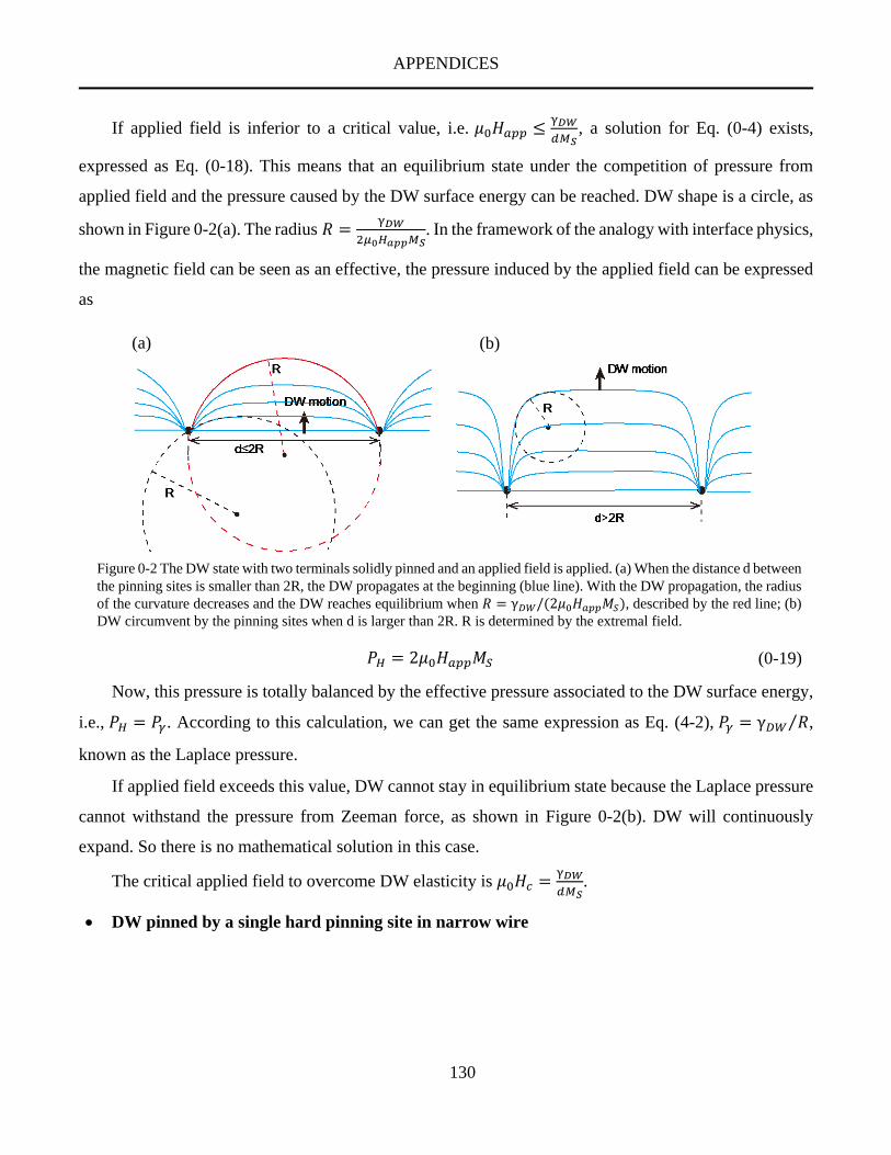
APPENDICES
130
If applied field is inferior to a critical value, i.e. 𝜇0𝐻𝑎𝑝𝑝 ≤γ𝐷𝑊
𝑑𝑀𝑆, a solution for Eq. (0-4) exists,
expressed as Eq. (0-18). This means that an equilibrium state under the competition of pressure from
applied field and the pressure caused by the DW surface energy can be reached. DW shape is a circle, as
shown in Figure 0-2(a). The radius 𝑅 =γ𝐷𝑊
2𝜇0𝐻𝑎𝑝𝑝𝑀𝑆. In the framework of the analogy with interface physics,
the magnetic field can be seen as an effective, the pressure induced by the applied field can be expressed
as
𝑃𝐻 = 2𝜇0𝐻𝑎𝑝𝑝𝑀𝑆 (0-19)
Now, this pressure is totally balanced by the effective pressure associated to the DW surface energy,
i.e., 𝑃𝐻 = 𝑃𝛾. According to this calculation, we can get the same expression as Eq. (4-2), 𝑃𝛾 = γ𝐷𝑊 𝑅⁄ ,
known as the Laplace pressure.
If applied field exceeds this value, DW cannot stay in equilibrium state because the Laplace pressure
cannot withstand the pressure from Zeeman force, as shown in Figure 0-2(b). DW will continuously
expand. So there is no mathematical solution in this case.
The critical applied field to overcome DW elasticity is 𝜇0𝐻𝑐 =γ𝐷𝑊
𝑑𝑀𝑆.
DW pinned by a single hard pinning site in narrow wire
(a) (b)
Figure 0-2 The DW state with two terminals solidly pinned and an applied field is applied. (a) When the distance d between
the pinning sites is smaller than 2R, the DW propagates at the beginning (blue line). With the DW propagation, the radius
of the curvature decreases and the DW reaches equilibrium when 𝑅 = γ𝐷𝑊/(2𝜇0𝐻𝑎𝑝𝑝𝑀𝑆), described by the red line; (b)
DW circumvent by the pinning sites when d is larger than 2R. R is determined by the extremal field.

APPENDICES
131
In the following, we discuss the DW behavior when one
of its terminals is solidly pinned by a hard pinning sites while
the other terminal can move freely along a wire. As shown in
Figure 2-2, we suppose that the one endpoint of the DW is
always fixed in (x1,0) while the other endpoint lies on the line
x=x2.
In this case, the expression of the free energy of the
system has the same expression as Eq. (0-3). To determine
the curve function of the DW in equilibrium state, we search
for the function 𝑓(𝑥) ∈ 𝐺′ that minimize the free energy of
the system, where 𝐺′ is a set of function {𝑓(𝑥)|𝑓(𝑥) ∈ 𝐶1(𝑥1, 𝑥2) 𝑎𝑛𝑑 𝑓(𝑥1) = 0}.
supposing 𝑓(𝑥) ∈ 𝐺′ is the function, then, the Eq. (0-6) applies also in this case, but g ∈ 𝐺′. After a
similar calculation, we can obtain the solution of the Eq. (0-6)
{
𝜕𝑒(�̂�,�̂�′)
𝜕𝑓′(𝑥)|𝑥2
∙ 𝑔(𝑥2) −𝜕𝑒(�̂�,�̂�′)
𝜕𝑓′(𝑥)|x1
∙ 𝑔(𝑥1) = 0
𝜕𝑒(�̂�,�̂�′)
𝜕𝑓(𝑥)−
𝜕
𝜕𝑥(𝜕𝑒(�̂�,�̂�′)
𝜕𝑓′(𝑥)) =0
𝑎𝑛𝑑 (0-20)
Since 𝑔(x1) = 0 is true but the value of 𝑔(𝑥2) is not fixed. The upper term of Eq. (0-20) requires,
𝜕𝑒(�̂�,�̂�′)
𝜕𝑓′(𝑥)|𝑥2
=�̂�′(𝑥2)
√1+�̂�′(𝑥2)2= 0 (0-21)
This means that the trajectory of the DW is always perpendicular to the line of x=x2 in this endpoint.
Using the similar integrations as given in Eq. (0-10) - (0-17), the lower term of Eq. (0-20) can be used
to deduce the function of the trajectory of DW. By considering the initial condition 𝑦0 = 𝑓(𝑥0), the final
solution is
𝑓(𝑥) = {√𝑅2 − (𝑥 − (𝑥2))
2− √𝑅2 − 𝐿2 𝑖𝑓 𝜇0𝐻𝑎𝑝𝑝 ≤
γ𝐷𝑊
2𝐿𝑀𝑆
𝑛𝑜 𝑠𝑜𝑙𝑢𝑡𝑖𝑜𝑛 𝑖𝑓 𝜇0𝐻𝑎𝑝𝑝 >γ𝐷𝑊
2𝐿𝑀𝑆
(0-22)
with R =γ𝐷𝑊
2𝜇0𝐻𝑎𝑝𝑝𝑀𝑆 and L=x2-x1.
in the case 𝜇0𝐻𝑎𝑝𝑝 ≤γ𝐷𝑊
2𝐿𝑀𝑆, the solution can also be written in the following expression,
(𝑥 − (𝑥2))2+ (𝑦 − (𝑦0 − √𝑅2 − 𝐿2))
2
= 𝑅2 (0-23)
Figure 0-3 Sketch showing a segment of DW
(black line) pinned by one hard pinning site
(x1,0) in one terminal and the other terminal
can move freely along the line x=x2.

APPENDICES
132
The above model can be ued to study the behavior of DW when only one of the endpoint is solidly
pinned by a hard pinning site in a wire. This hard pinning site may lie on the edge or inside the wire. The
other edge is relatively smooth, allowing the free displacement of the DW. As shown in Figure 0-4. We
can interpret this mathematical solution into the following physical pictures:
If applied field is inferior to a critical value, i.e. 𝜇0𝐻𝑎𝑝𝑝 ≤γ𝐷𝑊
2𝐿𝑀𝑆, DW can stay in an equilibrium state
under the competition of pressure from applied field and its elasticity. In this state, DW shape is a circle,
with one endpoint passing the pinning site and other endpoint lying in the edge and the DW trajectory is
perpendicular to the edge in this end, as shown in Figure 0-4(a).
If applied field exceeds this value, DW cannot stay in equilibrium state because DW elasticity cannot
withstand the pressure from Zeeman force, as shown in Figure 0-4(c). DW will circumvent from the
pinning site and depins. So there is no mathematical solution in this case.
Therefore, the critical applied field to overcome DW elasticity is 𝜇0𝐻𝑐 =γ𝐷𝑊
2𝐿𝑀𝑆. Under this threshold
field, the radius of DW circle equals to the distance from pinning site to the edge L.
It is to note that this solution is deduced under the assumption that the edge of wire is perfectly smooth.
In fact, due to the roughness of edge and intrinsic pinning field, DW depinning field from one hard pinning
site by circumventing should be larger than this critical value.
Figure 0-4 (a) DW pinned by a single hard pinning site when applied field 𝜇0𝐻𝑎𝑝𝑝 <γ𝐷𝑊
2𝐿𝑀𝑆;(b) applied field reaches the
critical field of depinning, 𝜇0𝐻𝑎𝑝𝑝 =γ𝐷𝑊
2𝐿𝑀𝑆, the radius of DW R=L; (c)when field 𝜇0𝐻𝑎𝑝𝑝 >
γ𝐷𝑊
2𝐿𝑀𝑆, DW circumvent from the
pinning site and depins.

APPENDICES
133
Appendix 2: Another example of magnetic sensors based on the elasticity
of DWs
Here, we show another effect related to the elasticity (surface tension) of DWs which can be used to
design DW based magnetic sensors. In a magnetic wire with a gradient width, we found that the DW
motion is reversible. As shown in Figure 0-5, in a magnetic wire with perpendicular magnetic anisotropy
(PMA), the width of the wire is 120 nm in left and 40 nm in right and the width gradually changes. A DW
was initially set in the right of wire. When a perpendicular field of 20 mT was applied, DW moves to the
left hand. When the external field was removed, the DW tended to spontaneously move to the right hand
and return to the initial position. This movement is possible since the motion of DW to the right will
decrease the DW length, thus minimizing the DW surface energy (this surface energy of DWs is the source
of the elasticity). The effective field produced by the DW elasticity is [29],
𝐻𝑒𝑓𝑓 =𝛾
2𝜇0𝑀𝑆𝑤∙𝑑𝑤
𝑑𝑥 (0-24)
Where w is w(x) is the width of the wire. We can see that this effective field is determined by w and
the gradient of w.
Since the design of magnetic sensors requires that the output signal has a monotonous and reversible
response to the input magnetic field, this phenomenon provides a possible way to design the DWs based
sensors.
Figure 0-5 The asymmetric DW motion in a wire with gradient of width (simulation results). From 0 to
12ns, an external field along ⊙ direction was applied and DW moves to left while from12ns to 25ns, DW
return to right spontaneously due to the effective field of elasticity.

APPENDICES
134
Here, we give an example based on the above mechanism. In a double-anchors shaped magnetic
structure with PMA, the gradient of the width increases from the middle to the terminals, as shown in
Figure 0-6. DW was set in the middle as the initial state. When an external field in ⊙ (or ⊗) presents,
DW move to left (right, respectively). Because of the gradient of the wire width, the effective field
produced by the DW elasticity increases as DW moves to the terminal. The position of the DW in the
stable state is determinated when the external is fixed. When the external field is removed, DW will return
to the initial position spontaneously due to the effective field of elasticity.
From the above example, we can see that the DW motion can show a monotonous and reversible
response to the external field. If the free layer of MTJs or spin valves is etched into this double anchors
structure, since the DW motion means a fluctuation of the magnetization, the motion can be characterized
by the change of the magneto-resistance thanks to the tunneling magnetoresistance or giant
magnetoresistance effect. In this way, the external field can be measured.
Figure 0-6 DW position in stable state under a certain external perpendicular field (simulation reults).

APPENDICES
135
Appendix 3: Experimental measurements of the resistivity of the CoFeB
thin film
Here, we summarized the information about the resistivity of CoFeB thin film based on experiments
performed on the similar structures as us. The resistivity of thin films
of CoFeB obtained varies from 160 to 330 μΩ·cm. In addition, the
composition of the CoFeB, the structure and the preparing condition
in these references are different from that of our and that the results
have a wide variation. In view that this value is of key importance for
the extraction of the polarization of CoFeB, we performed some
experiments to estimate the CoFeB thin film in our sample.
As shown in Figure 0-8 (b) & (c), 2cm×2cm films with two
different layer structures were deposited using sputtering: Substrate/MgO(2)/CoFeB(t)/Ta(5) and
Substrate/Ta(3)/CoFeB(t)/MgO(2)/Ta(2) with thickness in nm and t varying from 0 to 3. All these samples
Table 0-1 Resistivity of CoFeB in measured similar structures according to published results. Note that the structure of
our sample studied is Ta(5)/Co40Fe40B20/MgO(2)/Ta(5), annealed at 300°C for 2h.
Resistivi
ty of
CFB
(μΩ·cm)
Resistivi
ty of Ta
(μΩ·cm)
Composition
and structure
(thickness in
nm)
Thickn
ess of
CFB
(nm)
Anneali
ng
conditio
n
Measurement
method Reference
160 189
Sub/TaN(t)/
CoFeB(1)/M
gO(2)/Ta(1)
1 300°C, 1
h
R vs. thickness of
TaN in wire
J. Torrejon et
al. (2014), [78]
170 190 Si/Co40Fe40
B20/Ta(8) 4
unknow
n
R vs. thickness of
Ta in wire
Luqiao Liu et
al. (2012), [75]
330 --
W(2-7)/
Co32Fe48B
20/MgO
0.8-1.4 250°C,
30 min
R vs. thickness of
W in wire
(measured by TR-
MOKE)
S. Cho et al.
(2015) [150]
140 -- Co60Fe20B
20 100
350°C,1
h
four-point sheet
resistance meter
Y-T. Chen et al.
(2013) [169]
250 -- Co40Fe40B
20 10 No
four- point sheet
resistance meter
Y-T. Chen et al.
(2012) [170]
114 -- Co40Fe40B
20 bulk
Amorph
ous W. Kettler et al.
(1982) [171]
1
3 4
2
Figure 0-7 Schematic of the
configuration to measure the
square resistance of a film using
the four probes method.

APPENDICES
136
were annealed at 300°C for 2 hours and the composition are all Co40Fe40B20. The square conductance was
measured using the four probes method [167]. The measuring steps are: first, four pointed probes were
connected in the center of a 2cmx2cm sample. The four probes form a square and the size of the square is
far smaller than the sample, as shown in Figure 0-7. Second, a current 𝐼𝑖,𝑗 was applied via two of the
neighboring probes and the voltage 𝑉𝑘,𝑙was measured via the other two probes, where i, j, k, l are the index
of the probes. A resistance was obtained by 𝑅𝑖𝑗,𝑘𝑙 = 𝑉𝑘,𝑙 𝐼𝑖,𝑗⁄ . Then, this measurement was repeated by
changing the probes applying the current. At last, the square resistivity of the multi-layer stack can be
obtained with the following formula [167],
𝑅𝑆 =𝜋
2 ln2(𝑅12,34 + 𝑅23,41+𝑅34,12+𝑅41,23) (0-25)
The square conductance can be defined as 𝐺𝑆 = 1/𝑅𝑆. If the conductance of the multilayers stack can
be seen as the accumulation of the conductance of the Ta layers and the CoFeB layer,
𝐺𝑆 = 𝜎𝐶𝐹𝐵𝑡𝐶𝐹𝐵 + 𝜎𝑇𝑎𝑡𝑇𝑎 (0-26)
where 𝜎𝐶𝐹𝐵 and 𝜎𝑇𝑎 are the conductivity of CoFeB and Ta, 𝑡𝐶𝐹𝐵 and 𝑡𝑇𝑎 are the thickness of CoFeB and
Ta. If the thickness dependence of conductivity (Fuchs-Sondheimer model) [168] is neglected, the
conductance of the CoFeB can be extracted from the variation of Gs vs. the thickness of CoFeB, as plotted
in Figure 0-9.
According to the measurements on the Sub/MgO(2)/CoFeB(t)/Ta(5) structure, the resistivity of the
CoFeB is extracted to be 256 μΩ·cm; according to the measurements on the
Sub/Ta(3)/CoFeB(t)/MgO(2)/Ta(5) structure, the resistivity of CoFeB is extracted to be 168 μΩ·cm.
These results are close to the results measured by L. Liu et al. (2012), [75], J. Torrejon et al. (2014), [78].
However, the conductivity of the Ta is difficult to be extracted from our experiments since the thickness
Figure 0-8 (a) The multilayers structure of the sample studied; (b)&(c) Multilayers structures with thinner Ta layers
and varying thickness of CoFeB used for the measurement of the resistivity of CoFeB.

APPENDICES
137
of oxidized Ta is unknown. In the following analysis, we adopt the results of Liu et al. (2012), [75], i.e.,
𝜌𝐶𝐹𝐵 = 170 𝜇Ω ∙ 𝑐𝑚 and 𝜌𝑇𝑎 = 190 𝜇Ω ∙ 𝑐𝑚.
0 1 2 30.0005
0.0010
0.0015
0.0020
0.0025
Gs=1/Rs=σCFB
tCFB
+σTa
tTa
Square conductance
Linear fit
Gs (
S)
CoFeB thickness (nm)
Intercept 9.19269E-4
Slope 3.91437E-4
0.5 1.0 1.5 2.0 2.5 3.00.0005
0.0010
0.0015
0.0020
0.0025
Gs=1/Rs=σCFB
tCFB
+σTa
tTa
Exp. results
Linear fitting
Gs (
S)
CoFeB thickness (nm)
Intercept 5.671E-4
Slope 5.9703E-4
Figure 0-9 Square conductance of the film vs. the thickness of CoFeB in (a) the MgO(2)/CoFeB(t)/Ta(5) structure and
(b) in the /Ta(3)/CoFeB(t)/MgO(2)/Ta(2) structure. Note that the measurement of the square conductance on the sample
with 0nm CoFeB (a) and the sample with 0 and 0.5nm CoFeB (b) was failed because of the high contact resistance.
(a) (b)

APPENDICES
138
Appendix 4: More information about the DW depinning field in Figure
5-22
1. More detailed explanations about the measurement
In case (a), for DW motion on → direction, field pulses with magnitude of B=4.01mT and duration
T=5μs were used to drive DW from left to right for one time. All pinning sites with Bdep> 4.01 mT were
detected and measured. For DW motion in ← direction, the same method, all pinning sites with Bdep> 4.01
mT were measured.
In case (b), for both DW motion directions, field pulses with magnitude of B=4.63mT and duration
T=5μs were used to drive DW motion. However, not all the pinning sites above 4.63 mT are measured
because the pinning in this level are much thicker than case (a) and many pinning sites are masked by
others. However, all the pinning sites with Bdep>6mT are identified and plotted.
In case (c), for both DW directions, field pulses with magnitude of B=7.17 mT and duration T=5μs
were used to drive DW motion. All the pinning sites with Bdep>7.17 mT were identified and all the pinning
below this value were not identified.
In case (d), for both DW directions, the measurement was more rigorous, field pulses with magnitude
of B=6.88 mT and duration T=5μs were used to drive DW motion. All the pinning sites with Bdep>7.17
mT were identified and all the pinning sites blow 6.88 mT were not identified. It is to note that in the
lower case, i.e., for DW motion ←, I scanned two times with B=6.88 mT, but only four pinning sites are
found.
2. Analysis of the pinning sites in Figure 5-22 one by one
First, in case (c), the largest pinning site is n°8. Pinning n°8 is not the largest one in case (a) without
current, but become more obvious when current is applied in case (b); as the current further increased, in
case (c), the pinning was also enhanced and became much larger than the others. However, in case (d),
this pinning disappeared. It can be explained that this pinning site is in the top edge and it was enhanced
only in case (b) and (c).
In case (c), the second large pinning site is the pinning n°4, it is not measurable in case (a) and occurs
in (b) as current is applied. It becomes obvious in case (c) as current increases. However, it disappears in
case (d). It means that this pinning site is also in the top edge.

APPENDICES
139
Noting that pinning n°8 and pinning n°4 are very large for both the DW moving direction in (c) while
they disappear for both DW direction in (d). This is consistent with the prediction that they are both in the
top edge.
For case (d), the largest pinning site is pinning n°7. However, it disappears in case (b) and although
it appears in case (c), its pinning force is not so strong compared with others. The second large pinning
are n°2 and n°6, they exist in (c) but not so large compared with other pinnings. The third large pinning is
n°10 in case (d) but it disappears in case (c). Other examples about the incoherence between (c) and (d)
are pinning n°11, n°12, n°13, n°14 and n°15.
The pinning sites that seem correlated between (c) and (d) are pinning n°1, n°3, n°5 and n°6, i.e.,
these pinning are enhanced systematically. This nature conforms to the enhancement of intrinsic pinning
by SH current or enhancement of the pinning caused by the convoluted effect of edge roughness and some
huge defects inside the wire. Maybe the origin of these four pinning sites is very complex, being the hybrid
result of different cases.
In addition, as the largest pinning sites in case (a), including the pinning n°2, n°10, n°5, n°11 n°7 and
n°8 are enhanced by current either in case (c) and (d) and this enhancement is not correlated. This means
that most of the huge pinning we have measured are on either of the two edges, or very closed to the edge.
In summary, from the above analysis, we can see that the enhancement of the pinning effect by current
is not systematic. Most of them are enhanced either in case (c) or in (d). This conforms to the model of
SHE enhanced DW pinning effects caused by the huge defects in the edge. The pinning we measured is
the largest ones. When a current is applied, if the pinning in either of the two edges is enhanced, the largest
pinning we observed will increase. In addition, for the several pinning sites that is enhanced both in case
(c) and case (d), it conforms to the second model: SH current enhanced intrinsic pinning effect.

APPENDICES
140
Appendix 5: List of publications during the doctoral research
1. Zhang, Y.; Zhang, X. (co-first author); Hu, J.; Nan, J.; Zheng, Z.; Zhang, Z.; Zhang, Y.; Vernier,
N.; Ravelosona, D.; Zhao, W. Ring-shaped Racetrack memory based on spin orbit torque driven chiral
domain wall motions. Sci. Rep. 2016, 6, 35062, doi:10.1038/srep35062.
2. Zhang, X.; Vernier, N.; Zhao, W.; Vila, L.; Ravelosona, D. Extrinsic pinning of magnetic domain
walls in CoFeB-MgO nanowires with perpendicular anisotropy. AIP Adv. 2018, 8, 56307,
doi:10.1063/1.5006302.
3. Zhang, X.; Vernier, N.; Zhao, W.; Yu, H.; Vila, L.; Zhang, Y.; Ravelosona, D. Direct Observation
of Domain-Wall Surface Tension by Deflating or Inflating a Magnetic Bubble. Phys. Rev. Appl. 2018, 9,
24032, doi:10.1103/PhysRevApplied.9.024032.
4. Zhang, X.; Cai, W.; Zhang, X.; Wang, Z.; Li, Z.; Zhang, Y.; Cao, K.; Lei, N.; Kang, W.; Zhang,
Y.; Yu, H.; Zhou, Y.; Zhao, W. Skyrmions in Magnetic Tunnel Junctions. ACS Appl. Mater. Interfaces
2018, 10, 16887–16892, doi:10.1021/acsami.8b03812.
5. Zhang, L.; Zhang, X. (co-first author); Wang, M.; Wang, Z.; Cai, W.; Cao, K.; Zhu, D.; Yang,
H.; Zhao, W. Size dependence of the spin-orbit torque induced magnetic reversal in W/CoFeB/MgO
nanostructures. Appl. Phys. Lett. 2018, 112, 142410, doi:10.1063/1.5022824.
6. Zhang, Y.; Zhang, C.; Nan, J.; Zhang, Z.; Zhang, X.; Klein, J. O.; Ravelosona, D.; Sun, G.; Zhao,
W. Perspectives of Racetrack Memory for Large-Capacity On-Chip Memory: From Device to System.
IEEE Trans. Circuits Syst. I Regul. Pap. 2016, 63, 629–638, doi:10.1109/TCSI.2016.2529240.
7. Zhang, Y.; Zhang, X. (co-first author) ; Vernier, N.; Zhang, Z.; Agnus, G.; Coudevylle, J.; Lin,
X.; Zhang, Y.; Zhang, Y.; Zhao, W.; Ravelosona, D. Domain Wall Motion Driven by Laplace Pressure in
CoFeB-MgO Nanodots with Perpendicular Anisotropy. 2017. (Accepted by Physical Review Applied)
https://arxiv.org/abs/1711.11334
8. Zhang, X.; Vernier, N.; Cao, Z.; Leng, Q.; Cao, A.; Ravelosona, D.; Zhao, W. Magnetoresistive
sensors based on the elasticity of domain walls. arXiv 2018, 1–13, http://arxiv.org/abs/1801.01343.
9. Anni Cao, Xueying Zhang (co-first author) et al. Tuning the Dzyaloshinskii-Moriya Interaction
in Pt/Co/MgO heterostructures through MgO thickness (Accepted by Nanoscale)
https://arxiv.org/abs/1710.09051

RÉSUMÉ EN FRANÇAIS
141
Résumé en français
1. Motivation
Dans les films minces magnétiques, l'aimantation s'organise en domaines, qui sont des zones où
l'aimantation est uniforme. Le passage d'un domaine à l'autre se fait via une zone tampon très étroite
appelée "paroi de domaines" (acronyme : "DW" pour "Domain Wall"), dans laquelle l'aimantation change
progressivement de direction. Parmi les mécanismes qui permettent d'expliquer le retournement de
l'aimantation du film considéré, celui le plus couramment rencontré est la nucléation d'un petit domaine
en un point de facile retournement, suivi de la propagation de la paroi ainsi apparue. De ce fait, les parois
de domaines peuvent être considérées comme des pseudo-objets et l'étude de leur comportement est un
des gros enjeux actuels. Par exemple, via des expériences bien choisies, cela permet d'accéder à certains
paramètres fondamentaux tels que l'aimantation à saturation MS [1], la rigidité d'échange A ou la constante
d'amortissement α.
La maitrise de la propagation des parois de domaines est un très gros enjeu actuel, car beaucoup de
dispositifs de stockage d'informations et de traitement de données sont basés sur la manipulation de la
structure en domaines. Par exemple, citons des dispositifs logiques à base de parois de domaines [6,7] ou
des réseaux neuronaux artificiels basés sur des parois de domaines [8–10]. Les parois de domaines peuvent
être aussi utilisées comme canal de transmission d'ondes de spin [11]. La proposition du concept de
mémoire de type Racetrack par S. Parkin [12,13], qui stocke sur des nanofils magnétiques, a déclenché
une explosion soutenue des recherches sur les mouvements des parois de domaines dans les nanofils.
Au cours des deux dernières décennies, le mouvement de parois de domaines induit par courant
polarisé en spin est apparu comme une nouvelle technique prometteuse, car elle peut permettre un
mouvement de translation globale de toute la structure en domaines, contrairement au mouvement induit
par champ magnétique, qui ne peut que faire grandir les domaines bien orientés. Mais, cette technique est
loin d'être maitrisée, car, souvent, de nombreux phénomènes s'entremêlent lorsqu'on la met en oeuvre. Il
y a d'abord le couple de transfert de spin (usuellement appelé STT pour Spin Tranfer Torque), qui apparait
lorsqu'un courant polarisé en spin traverse la paroi, et qui peut se décomposer en deux contributions
(adiabatique et non adiabatique). Il y a aussi l'interaction spin-orbite (SOT, Spin Orbit Torque), qui peut
introduire un couple supplémentaire pour déplacer les parois via des mécanisme tels que l’Effet Hall de
Spin (SHE, Spin Hall Effect) lorsque le film magnétique a été déposé sur un métal non magnétique. Du
fait de la présence de nombreuses interfaces dans les multicouches magnétiques utilisées, il peut être aussi

RÉSUMÉ EN FRANÇAIS
142
nécessaire de prendre en compte l’interaction de Dzyaloshinskii-Moriya (DMI, Dzyaloshinskii-Moriya
Interaction). Ces différents mécanismes ouvrent des perspectives très intéressantes, puisqu'ils permettent
de déplacer les parois de domaines à des vitesses beaucoup plus élevées que le champ magnétique.
Dans le cadre de ce travail, nous nous sommes concentrés sur un matériau émergent en vue des
applications, qui est le CoFeB [14–18] : il a un faible coefficient d'amortissement et un faible champ de
dépiégeage, ce qui promet une meilleure efficacité pour les dispositifs basés sur des parois du domaine.
La structure de ces films fait qu'ils faut potentiellement prendre en compte tous les effets évoqués ici, ce
qui rend le comportement de ces films complexes. Le rôle des différents mécanismes sur le mouvement
des parois doit être clarifié.
Cette thèse se concentre sur l'étude des propriétés statiques et dynamiques des parois de domaines
dans des nanofils CoFeB. Certaines propriétés peuvent se comprendre de manière très simple à l'aide du
concept d’énergie interfaciale. D'autres problèmes, tels que le piégeage des parois ou la détermination de
l'efficacité du couple de transfert de spin, nécessite une analyse plus poussée. Pour déterminer certains
paramètres fondamentaux tels que le taux de polarisation en spin des porteurs de charge, la propagation
induite par un champ magnétique et un courant électrique simultanément appliqués apporte des
renseignements nouveaux et très importants.
2. Echantillons et méthodes
Les échantillons étudiées sont des couches minces de Ta(5nm)/Co40Fe40B20(1nm)/MgO(2
nm)/Ta(5nm) avec anisotropie perpendiculaire. Ils sont structurés aux nanofils longs de 50 μm, avec un
plot de nucléation. Les largeurs des fils sont : 200 nm, 400 nm, 600 nm, 1 μm et 1.5 μm. Certains nanofils
présentent des croix de Hall pour les mesures électriques. Toutes les structures sont équipées d'électrodes
pour des tests électriques. Il est à noter que la constante DMI mesurée dans notre système est très faible,
inférieure à 0,01 mJ/m2, et ces interactions peuvent être négligées.
Les observations du comportement des parois ont été réalisées grâce à un microscope Kerr, capable
de visualiser l'état magnétique des nanofils jusqu'à la largeur de 200 nm. L'utilisation de champs
magnétiques impulsionnels est apparue comme un outil essentiel pour nos études. Avec une petite bobine
de 120 tours et de 6 mm de rayon, alimentées par un générateur d'impulsion haute tension, nous avons pu
créer une impulsion de champ magnétique d'amplitude 130 mT, ayant un temps de montée de 1.9 μs. Ce
type d'impulsions très courtes permet de créer une paroi de domaine dans une nanostructure, sans pour
autant retourner toute la structure du fait de la propagation qui s'ensuit, et, donc, de conserver une structure
multidomaine avec présence de paroi dans la nanostructure. Avec une bobine de 20 tours, nous avons pu

RÉSUMÉ EN FRANÇAIS
143
réduire le temps de montée de l'impulsion de champ à 220 ns. Cela nous a permis de mesurer la vitesse de
mouvement des parois dans nos nanofils de manière précise. Pour terminer, les impulsions de champ ont
pu être synchronisées avec une impulsion de courant électrique à travers le nanofils, pour étudier le
comportement des parois sous l’effet combinée de ces deux actions.
3. Résultats
a. L’énergie interfaciale des parois du domaine
Nous avons d'abord pu mettre en évidence le rôle dominant et direct de la tension interfaciale de paroi
dans certaines expériences. D'habitude, cette tension n'apparait que de manière très indirecte.
Pour commencer, nous avons observé qu'une bulle magnétique semi-circulaire dans un petit carré
devenait instable et disparaissait spontanément lorsque le champ externe est nul. Nous avons expliqué cela
grâce à la pression de Laplace induite par l'énergie interfaciale lorsque la paroi de domaine présente une
courbure. En vérifiant le champ magnétique nécessaire pour stabiliser le domaine semi-circulaire, nous
avons pu estimer l'énergie interfaciale des parois dans notre structure, nous avons obtenu 5,4 mJ/m2.
Ensuite, nous avons observé l'effet de l'interaction entre deux bulles semi-circulaires dans le petit
carré constitué par le plot de nucléation lorsqu'un champ externe est appliqué. La bulle plus grosse
commence par croitre de manière continue. Lorsque les deux bulles sont assez proches, la répulsion
dipolaire induit la contraction de la bulle plus petite jusqu'à sa disparition. Cette expérience fait penser à
Figure 1 Images optique de deux des échantillons étudiés, (a) avec et (b)
sans la croix de Hall. La zone entourée par la ligne pointillée rouge est la
structure magnétique. Les parties jaunes sont des électrodes.

RÉSUMÉ EN FRANÇAIS
144
celle classique (pour les spécialistes des mousses) des deux bulles de savon reliées, dans laquelle la grosse
bulle "mange" la petite. Cela est encore une fois expliqué par la pression de Laplace, qui est plus grande
pour la petite bulle.
Pour finir, nous avons identifié l'origine de piégeage de la paroi auprès des croix du Hall ou à la
connexion entre un fil étroit et un grand plot magnétique. C'est encore la pression de Laplace qui intervient.
En effet, la force liée à l'énergie interfaciale doit être surmontée quand la paroi commence à se dilater dans
le plot. Conformément aux prédictions théoriques, nous avons constaté que le champ de dépiégeage
augmente de façon proportionnelle à 1/w, où w est la largeur du fil. L'étude du champ de dépiégeage en
fonction de 1/w apparaît comme une très bonne méthode pour mesurer l'énergie de interfaciale de paroi
du domaine. Grâce à cette deuxième méthode, nous avons refait une mesure de l'énergie de interfaciale de
parois, qui a donné 4,1 mJ/m2, ce qui est en bon accord avec notre première valeur compte-tenu des
incertitudes expérimentales.
Nos expériences ont montré l'importance de l'énergie interfaciale de paroi: elles expliquent le
piégeage de paroi dans des nanofils dus à des défauts ou des encoches, notamment aux croix de Hall, ce
qui est critique pour des applications telles que la mémoire de type "racetrack". De plus, notre méthode
de mesure de l'énergie interfaciale pourrait être très utile dans l'étude des couches minces présentant le
DMI, car ces interactions modifient radicalement l'énergie interfaciale [23].
Enfin, un nouveau prototype de capteur magnétique basé sur la tension interfaciale (ou l’élasticité)
des parois du domaine magnétique a été proposé et émulé avec des simulations micromagnétiques. Ces
nouveaux capteurs montrent une bonne performance sur la mesure du champ direct ou alternatif. Des
Figure 2 Contraction spontanée de la bulle de domaine semi-circulaire dans un champ
externe nul.

RÉSUMÉ EN FRANÇAIS
145
performances telles que la plage de mesure et la sensibilité peuvent être ajustées en manipulant la
géométrie et la taille ou le dispositif. Le dispositif proposé peut améliorer le niveau d'intégration et les
performances des capteurs magnétiques.
b. Le mouvement des parois et l’effet de piégeage dans des nanofils
Pour commencer, nous avons vérifié les vitesses de propagation des parois dans des nanofils induit
par le champ magnétique, ainsi que les positions des plus gros défauts de piégeage et le champ critique de
dépiégeage associé à chacun de ces défauts.
Nous avons constaté une augmentation du champ de dépiégeage des plus gros défauts proportionnelle
à 1/w, w étant la largeur des pistes (figure 3). Cela nous a conduit à penser que ces gros défauts sont de
nature extrinsèque, c'est-à-dire liés à la rugosité des bords des fils induite par la nanostructuration.
Ensuite, la vitesse de mouvement de paroi induit par impulsion du champ et de courant synchronisées
a été mesurée. En régime précessionnel (champ magnétique élevé), il est prévu que la vitesse du
mouvement de la paroi induit par l'effet combiné du champ et du STT est égale à la somme VB+VJ, où VB
aurait été la vitesse obtenue en appliquant uniquement le champ magnétique et VJ=gµBPj/2eM est une
vitesse de dérive des porteurs de charge, j étant la densité de courant, µB le magnéton de Bohr, M la densité
d'aimantation, e la charge d'un porteur et P le taux de polarisation des porteurs de charge(figure 4 et 5).
Figure 3. histogramme de distribution du champ de dépiégeage des défauts les plus forts, en
utilisant les cinq défauts les plus forts pour chaque fil inclus dans les statistiques.

RÉSUMÉ EN FRANÇAIS
146
Nos résultats expérimentaux s'avèrent en remarquable accord avec cette prédiction (figure 5). La
pente de la figure 5 nous permet d'accéder au taux de polarisation P : nous avons trouvé P=26%. Cette
valeur est très inférieure à la polarisation mesurée par la réflexion Point-Contact Andreev (65%) [151] ou
par la spectroscopie tunnel supraconductrice (53%) [91–93]. La diffusion des électrons et les effets de
couplage spin-orbite dans la couche de Ta sont des explications possibles pour expliquer la faible
polarisation de spin dans cette structure.
Figure 4. Vitesses de mouvement de la paroi du domaine induites par différents champs et
densités de courant. Le courant circulant le long de la direction de mouvement de la paroi
est défini comme positif. Les vitesses dans le plateau, encadrées par la ligne verte en
pointillés, sont moyennées et représentées en fonction du courant de la figure 5.
-4 -2 0 2 4
0
2
4
6
8
10
Exp. results
Linear fitting
DW
velo
city
(m
/s)
Current (mA)
Intercept 4.90717
Slope -1.21376
Figure 5 Vélocités moyennes obtenues à partir des résultats de la figure 4
(encadrés en vert). La barre d'erreur a été prise comme l'écart-type. La ligne
rouge est un ajustement linéaire sur toutes ces vitesses.
RÉSUMÉ EN FRANÇAIS
147
De plus, nous avons constaté que le champ de dépiégeage liés aux gros défauts des nanofils
augmentait de façon significative lorsqu'un courant était appliqué simultanément au champ magnétique,
quelle que soit la direction de mouvement de la paroi par rapport à la direction de courant d’électrique.
Une explication possible de cet effet est un courant de Spin Hall (SH) provenant de la couche de Ta au-
dessous, qui induirait un couple supplémentaire. L'effet de ce couple été testé de manière numérique, nos
calculs ont débouchés sur un renforcement du piégeage dans certains cas. Cependant, seuls les effets de
piégeage extrinsèques sur l'un des deux bords peuvent être renforcée.
Pour finir, un dispositif de mémoire de type racetrack en forme d'anneau basé sur le mouvement de
paroi induit par les effets combinés de STT et SOT dans des nanofils a été conçu et émulé à l'aide de
calculs micromagnétiques. Ce type de dispositif permet d'éviter la perte de données par rapport à la
mémoire de racetrack traditionnelle en forme de ligne.
4. Conclusions et perspectives
Dans cette thèse, nous avons étudié les propriétés et la dynamique des parois de domaines
magnétiques dans des films de CoFeB à anisotropie perpendiculaire. Des phénomènes dus à la tension
interfaciale des parois ont été observées et la valeur de l’énergie interfaciale a été quantifiée directement.
L’effet de piégeage des parois dans des nanofils a été étudié, il est apparu que les plus gros défauts seraient
de nature extrinsèque, c'est-à-dire liés à la rugosité de bord induite par la nanostructuration. Le mouvement
des parois dans des nanofils induit par le champ et par l’effet combiné du champ et de courant a été étudié.
Cela nous a permis d'évaluer le taux polarisation des porteurs de charge dans le CoFeB. Le faible taux
trouvé permet d'expliquer les difficulté rencontrées par les différentes équipes pour mettre en mouvement
les parois uniquement avec du courant.
D'autres études sont nécessaires pour poursuivre ce projet :
Les deux méthodes développées pour mesurer la tension interfaciale des parois du domaine peuvent
être utilisées pour quantifier la constante de DMI et la rigidité d'échange A, paramètres difficiles à mesurer
actuellement.
Les effets du courant de SH provenant de la couche de Ta peuvent expliquer le renforcement des
effets de piégeage de paroi dans le fil étroit lorsqu'un courant est appliqué. Mais, cette explication n'a été
testée qu'avec des simulations micromagnétiques. D'autres expériences sont nécessaires pour étudier cet
effet et déterminer si l'origine de notre effet peut être expliqué ainsi. Par exemple, on peut graver des
encoches régulières dans le bord des fils pour observer l'influence du courant sur les effets de piégeage de
paroi. Le fil peut aussi être agrandi à plus de 10 micromètres de sorte que le comportement des parois

RÉSUMÉ EN FRANÇAIS
148
pourra être observé clairement, par exemple, l'angle d'inclinaison de la paroi devrait varier en fonction de
la densité de courant appliquée, comme prédit par la théorie. L'angle de SH pourrait être extrait de ces
expériences.
En ce qui concerne le mouvement de paroi induit champ magnétique et le courant simultané, s'il est
vrai qu'il peut être expliqué par les effets combinés du champ et du STT, dans la structure métal
lourd/couche magnétique/MgO, il faudrait prendre en compte le courant SH provenant de la couche de
métal lourd. Il pourrait être intéressant de mettre en œuvre un champ dans le plan en plus du système
actuel et d'étudier l'effet combiné du champ magnétique, du STT et du SOT sur le mouvement de paroi.
Certains paramètres importants tels que l'angle SH, la constante non-adiabatique pourraient être
correctement extraites grâce à de telles expériences.

Université Paris-Saclay Espace Technologique / Immeuble Discovery Route de l’Orme aux Merisiers RD 128 / 91190 Saint-Aubin, France
Titre : Le mouvement des parois des domaines magnétiques dans le fil de CoFeB induit par le courant polarisé
Mots clés : Paroi de domaine magnétique, Microscopie Kerr, Nanofil de CoFeB, Tension interfaciale, Couple de transfert de spin, Magnétisme
Résumé : Cette thèse est consacrée aux recherches des propriétés statiques et dynamiques des parois de domaines magnétiques (DW pour Domain Wall) dans les nanofils CoFeB. Un système de mesure basé sur un microscope Kerr à haute résolution a été mis en place et utilisé pour ces recherches. Tout d'abord, les phénomènes liés à la tension interfaciale des parois ont été étudiés. La contraction spontanée des bulles de domaine a été observée directement en utilisant le microscope Kerr. Ce phénomène a été expliqué en utilisant le concept de la pression de Laplace due à l'énergie interfaciale des parois. L'énergie interfaciale des parois a été quantifiée en mesurant le champ externe nécessaire pour stabiliser ces bulles. Le mécanisme de la piégeage et de la dépiégeage des parois dans certaines géométries artificielles, comme la croix de Hall ou l'entrée reliant un carré de nucléation et un fil, a été expliqué en utilisant le concept de tension interfaciale des parois et a été utilisé pour extraire l'énergie interfaciale des parois. Bénéficiant de ces études, une méthode permettant de quantifier directement le coefficient des Interactions de Dzyaloshinskii- Moriya (DMI pour Dzyaloshinskii- Moriya Interaction) à l'aide du microscope Kerr a été proposée. En outre, un nouveau type de capteur magnétique basé sur l'expansion réversible de paroi en raison de la tension interfaciale a été proposé et vérifié en utilisant des simulations micromagnétiques. Deuxièmement, les propriétés dynamiques des parois dans le film et les fils Ta / CoFeB / MgO ont été étudiées. La vitesse du propagation des parois induite par le champ magnétique ou par l'effet combiné des impulsions de champ magnétique synchronisées et des impulsions de courant électrique a été mesurée. En régime
précessionne, la vitesse du mouvement DW induite par l'effet combiné du champ et du courant est égale à la superposition des vitesses entraînées par le champ ou le courant indépendamment. Ce résultat nous a permis d'extraire la polarisation de spin de CoFeB dans cette structure. Les effets de piégeage du mouvement des parois dans les fils étroits ont été étudiés. Des champs de dépiégeage associés aux gros défauts pour le mouvement des parois induit par champ dans les nanofils a été mesurée. Il a été constaté que les effets de piégeage deviennent plus sévères lorsque la largeur w des fils diminue. Une relation linéaire entre le champ de piégeage et 1/w a été trouvée. L'origine de ces sites d'ancrage durs ainsi que leurs influences sur la vitesse de mouvement des parois ont été discutées. En outre, il a été constaté que l'effet d'épinglage était amélioré lorsque le courant était appliqué, quelle que soit la direction relative entre le mouvement des parois et le courant. Cet accroissement pourrait être expliqué par l'effet du courant de Hall de spin de la sous-couche (Ta). Bien qu'il n'y ait pas eu de DMI ou de champ planaire, le courant de Hall de spin, polarisé dans la direction transversale, peut exercer un couple sur la parois de type de Bloch, une fois que la paroi s'éloigne de la direction transversale. Enfin, un dispositif mémoire de circuit en forme d'anneau basée sur le travail combiné de STT et SOT a été proposée. Comparée à la mémoire de piste traditionnelle en forme de ligne, cette mémoire en forme d'anneau permet au paroi de demaine de se déplacer dans un nanofil en forme d'anneau sans être éjecté, évitant ainsi la perte des informations associées. Le travail de conception et d'optimisation a été réalisé avec des simulations micromagnétiques.

Université Paris-Saclay Espace Technologique / Immeuble Discovery Route de l’Orme aux Merisiers RD 128 / 91190 Saint-Aubin, France
Title : Spin-polarized current-induced domain wall motion in CoFeB nanowires
Keywords : Domain Wall (DW), Kerr microscopy, CoFeB nanowire, Surface tension, Spin transfer torque (STT), Magnetism
Abstract : This thesis is dedicated to the research of the static and dynamic properties of magnetic Domain Walls (DWs) in CoFeB nanowires. A measurement system based on a high-resolution Kerr microscope was implemented and used for these research. First, phenomena related to the DW surface tension was studied. A spontaneous collapse of domain bubbles was directly observed using the Kerr microscope. This phenomenon was explained using the concept of the Laplace pressure due to the DW surface energy. The surface energy of DW was quantified by measuring the external field required to stabilize these bubbles. The DW pinning and depinning mechanism in some artificial geometries, such as the Hall cross or the entrance connecting a nucleation pad and a wire, was explained using the concept of DW surface tension and was used to extract the DW surface energy. Benefited from these studies, a method to directly quantify the coefficient of Dzyaloshinskii- Moriya Interactions (DMI) using Kerr microscope has been proposed. In addition, a new type of magnetic sensor based on the revisable expansion of DW due to DW surface tension was proposed and verified using micromagnetic simulations. Second, the dynamic properties of DWs in Ta/CoFeB/MgO film and wires were studied. The velocity of DW motion induced by magnetic fields or by the combined effect of synchronized magnetic field pulses and electrical current pulses was measured. In steady
flow regime, the velocity of DW motion induced by the combined effect of the field and the current equals to the superposition of the velocities driven by field or current independently. This result allowed us to extract the spin-polarization of CoFeB in this structure. Pinning effects of DW motion in narrow wires was studied. Depinning fields of hard pinning sites for the field-driven DW motion in nanowires was measured. It was found that the pinning effects become severer as the width w of the wires scaled down. A linear relationship between the depinning field and w was found. The origin of these hard pinning sites, as well as their influences on the DW motion velocity, was discussed. Furthermore, it was found that the pinning effect was enhanced when a current was applied, no matter the relative direction between the DW motion and the current. We propose a possible explanation, which would be an effect of the spin Hall current from the sublayer (Ta). Although there was no DMI or in-plane field, the spin Hall current, which was polarized in the transverse direction, can still exert a torque on the Bloch DW, once the DW tilts away from the transverse direction. At last, a ring-shaped racetrack memory based on the combined work of STT and has been proposed. Compared with the traditional line-shaped racetrack memory, this ring-shaped memory allows the DW moving in a ring-shaped nanowire and the data dropout problem can be avoided. The design and optimization work was performed with micromagnetic simulations.