spin-dependent recombination in czochralski silicon ... · spin-dependent recombination in...
TRANSCRIPT

Spin-dependent recombination in Czochralski silicon containing oxideprecipitates
V. Lang,1,a) J. D. Murphy,1 R. J. Falster,1,2 and J. J. L. Morton1,31Department of Materials, University of Oxford, Oxford OX1 3PH, United Kingdom2MEMC Electronic Materials Inc., Viale Gherzi 31, Novara 28100, Italy3CAESR, Clarendon Laboratory, Department of Physics, University of Oxford, Oxford OX1 3PU,United Kingdom
(Received 25 October 2011; accepted 8 December 2011; published online 10 January 2012)
Electrically detected magnetic resonance is used to identify recombination centers in a set ofCzochralski-grown silicon samples processed to contain strained oxide precipitates with a widerange of densities (! 1"109 cm#3 to ! 7"1010 cm#3). Measurements reveal that photo-excitedcharge carriers recombine through Pb0 and Pb1 dangling bonds, and comparison to precipitate-freematerial indicates that these are present at both the sample surface and the oxide precipitates. Theelectronic recombination rates vary approximately linearly with precipitate density. Additionalresonance lines arising from iron-boron and interstitial iron are observed and discussed. Ourobservations are inconsistent with bolometric heating and interpreted in terms of spin-dependentrecombination. Electrically detected magnetic resonance is thus a very powerful and sensitivespectroscopic technique to selectively probe recombination centers in modern photovoltaic devicematerials.VC 2012 American Institute of Physics. [doi:10.1063/1.3675449]
I. INTRODUCTION
Oxygen is an important impurity in silicon, being pres-ent in concentrations of ! 1018 cm#3 in Czochralski silicon(Cz-Si), which is used for the vast majority of integrated cir-cuits (ICs) and ! 40% of solar cells. It is also present in lower,but still significant, concentrations (of order 1017 cm#3) in castmulticrystalline silicon (mc-Si) used equally, if not morewidely, for modern silicon photovoltaics. The presence ofoxygen has substantial beneficial as well as detrimentaleffects on silicon’s material properties and so has been thesubject of much research (see Refs. 1 and 2). Perhaps mostimportantly, oxide precipitates (OPs) can be intentionallycreated in inactive regions of wafers to act as sinks for detri-mental metallic impurities in a process known as internalgettering.3–5 Oxygen can also improve high-temperature me-chanical strength by atomic decoration of dislocations6 andby precipitation in the bulk.7 Unfortunately, oxygen-containing defects in various guises also act as recombina-tion centers, including thermal donor defects,8 boron-oxygencomplexes,9,10 and OPs.11,12 OPs can also form unintention-ally in mc-Si during ingot cooling13 and can limit the effi-ciency of modern silicon photovoltaic devices.14 Theyundergo a morphological transformation during growth,15,16
which is known to have implications for both internal getter-ing15 and recombination of minority carriers.12 The precipi-tates initially exist in an unstrained state (sometimes referredto as “ninja particles”), but, after a certain threshold growthtime (dependent on the density of nucleation sites),they change morphology into a strained state, which coin-cides with the transition from ineffective to totally effective
gettering.15 They then continue to grow in size and eventu-ally begin to become surrounded by complex dislocationstructures and even stacking faults.15 Recombination at OPshas recently been found to depend upon their strain state andwhether the precipitates are surrounded by other extendeddefects.12 Interestingly, the rate of recombination in samplesdominated by strained precipitates is dependent upon precip-itate density rather than size.12 As the number of corners ofthe strained platelets is invariant with size, these discontinu-ities have been suggested to play a role in the recombinationprocess.12 The photoconductance methods17 used in this pre-vious study12 do, however, not allow the microscopic natureof the specific defect(s) responsible for recombination to beclearly determined.
In this paper, we present the results of experiments usingelectrically detected magnetic resonance (EDMR), whichaim to better understand the recombination mechanism asso-ciated with OPs. EDMR is a sensitive spectroscopic tech-nique, providing a much higher sensitivity than conventionalelectron paramagnetic resonance (EPR) for bulk samples,which has been used extensively to study defects and impur-ities in silicon.18–23 The sensitivity of EDMR is typically! 106 times higher than for conventional EPR and has beendemonstrated to approach the few to single-spin regime fornanodevices with an optimized sample geometry.24,25 InEDMR, the sample is placed in a static magnetic field andirradiated in a microwave cavity. The EPR-induced changein spin population is detected through the (resonant) changeof the device conductivity. Hence, only electrically activedefects involved in electron transport, such as recombinationcenters, are observed in EDMR. As opposed to EPR, para-sitic signals, which do not determine electron transport, areconsequently not observed. This is why EDMR has been par-ticularly successful in the spectroscopic characterization of,
a)Author to whom correspondence should be addressed. Electronic mail:[email protected].
0021-8979/2012/111(1)/013710/7/$30.00 VC 2012 American Institute of Physics111, 013710-1
JOURNAL OF APPLIED PHYSICS 111, 013710 (2012)
e.g., electron transport in silicon field-effect transistors26 aswell as defects and impurities in modern silicon photovoltaicdevices.27 Magnetic resonance techniques have also beenused previously to study recombination at OPs,28,29 showing,for example, that silicon dangling bonds at the silicon-silicondioxide interface (Si/SiO2) play a major role in recombina-tion at OPs.28 In our work, we study materials possessing awide range of strained precipitate densities, which we relateto spin-dependent recombination times extracted from theEDMR data. We also study intentionally iron-contaminatedsamples to improve understanding of the role of interstitialiron (Fe) in the recombination process.
II. EXPERIMENTAL METHODS
A. Growth of oxide precipitates
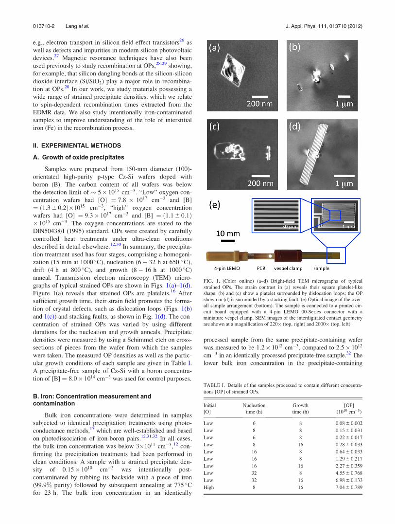
Samples were prepared from 150-mm diameter (100)-orientated high-purity p-type Cz-Si wafers doped withboron (B). The carbon content of all wafers was belowthe detection limit of ! 5" 1015 cm#3. “Low” oxygen con-centration wafers had [O] $ 7:8 " 1017 cm#3 and [B]$ %1:36 0:2&"1015 cm#3, “high” oxygen concentrationwafers had [O] $ 9:3" 1017 cm#3 and [B] $ %1:16 0:1&" 1015 cm#3. The oxygen concentrations are stated to theDIN50438/I (1995) standard. OPs were created by carefullycontrolled heat treatments under ultra-clean conditionsdescribed in detail elsewhere.12,30 In summary, the precipita-tion treatment used has four stages, comprising a homogeni-zation (15 min at 1000 'C), nucleation (6# 32 h at 650 'C),drift (4 h at 800 'C), and growth (8# 16 h at 1000 'C)anneal. Transmission electron microscopy (TEM) micro-graphs of typical strained OPs are shown in Figs. 1(a)–1(d).Figure 1(a) reveals that strained OPs are platelets.16 Aftersufficient growth time, their strain field promotes the forma-tion of crystal defects, such as dislocation loops (Figs. 1(b)and 1(c)) and stacking faults, as shown in Fig. 1(d). The con-centration of strained OPs was varied by using differentdurations for the nucleation and growth anneals. Precipitatedensities were measured by using a Schimmel etch on cross-sections of pieces from the wafer from which the sampleswere taken. The measured OP densities as well as the partic-ular growth conditions of each sample are given in Table I.A precipitate-free sample of Cz-Si with a boron concentra-tion of [B] $ 8:0" 1014 cm#3 was used for control purposes.
B. Iron: Concentration measurement andcontamination
Bulk iron concentrations were determined in samplessubjected to identical precipitation treatments using photo-conductance methods,17 which are well-established and basedon photodissociation of iron-boron pairs.12,31,32 In all cases,the bulk iron concentration was below 3"1011 cm#3,12 con-firming the precipitation treatments had been performed inclean conditions. A sample with a strained precipitate den-sity of 0:15" 1010 cm#3 was intentionally post-contaminated by rubbing its backside with a piece of iron(99:9% purity) followed by subsequent annealing at 775 'Cfor 23 h. The bulk iron concentration in an identically
processed sample from the same precipitate-containing waferwas measured to be 1:2" 1012 cm#3, compared to 2:5" 1012
cm#3 in an identically processed precipitate-free sample.32 Thelower bulk iron concentration in the precipitate-containing
FIG. 1. (Color online) (a–d) Bright-field TEM micrographs of typicalstrained OPs. The strain contrast in (a) reveals their square platelet-likeshape. (b) and (c) show a platelet surrounded by dislocation loops; the OPshown in (d) is surrounded by a stacking fault. (e) Optical image of the over-all sample arrangement (bottom). The sample is connected to a printed cir-cuit board equipped with a 4-pin LEMO 00-Series connector with aminiature vespel clamp. SEM images of the interdigitated contact geometryare shown at a magnification of 220" (top, right) and 2000" (top, left).
TABLE I. Details of the samples processed to contain different concentra-tions [OP] of strained OPs.
Initial[O]
Nucleationtime (h)
Growthtime (h)
[OP](1010 cm#3)
Low 6 8 0:086 0:002
Low 8 8 0:156 0:031
Low 6 8 0:226 0:017
Low 8 16 0:286 0:033
Low 16 8 0:646 0:033
Low 16 8 1:296 0:217
Low 16 16 2:276 0:359
Low 32 8 4:556 0:768
Low 32 16 6:986 0:133
High 8 16 7:046 0:789
013710-2 Lang et al. J. Appl. Phys. 111, 013710 (2012)
sample strongly indicates that ! 1" 1012 cm#3 of the bulkiron is gettered to the OPs and associated defects.
C. EDMR experiments
Interdigitated chromium/gold (10/30nm) thin films weredefined by electron-beam lithography on a JEOL JBX-5500FS system and used to electrically contact the activearea of the device with a minimal resistivity and without per-turbing the microwave field in the cavity. All samples werediced into small chips of 2" 20 mm2 in size and connectedto a printed circuit board with a miniature vespel clamp, asshown in Fig. 1(e). The maximum diameter of the overallarrangement was chosen so that it can be inserted into a glasstube with an outer diameter of 5mm to protect the sampleagainst mechanical damage during its insertion into the cav-ity and vibration during the measurement. EDMR was per-formed with a modified Bruker ESP380-1010 pulsed X-bandEPR spectrometer and an Oxford Instruments CF-935 he-lium-gas flow cryostat in combination with an Oxford Instru-ments ITC-503S temperature controller. The microwaveexcitation was generated with an Agilent TechnologiesE8267D PSG vector signal generator and applied by aBruker ER4118X-MD5-W1 X-band dielectric ring resonatoroperating at a DC magnetic field B0 ! 0:35 T. The magneticfield was aligned perpendicular to the growth direction of thesample, i.e., B0 k (100) (unless otherwise indicated). Mag-netic field modulation was applied with a HP 33120A func-tion generator in order to enhance the signal-to-noise ratio.This lock-in technique results in the EDMR signal appearingas the first derivative of the sample resistivity with respect tomagnetic field, i.e., @%Dq=q0&=@B, where q0 denotes thesample resistivity in thermal equilibrium. Beside enhancingthe signal-to-noise ratio, this lock-in technique also allowsthe Lande g factor to be measured more accurately, as thezero-crossing of the first derivative line is easier to determinethan the position of the maximum of the EDMR absorptionline. The magnetic field, as well as the modulation ampli-tude, was calibrated with a 2,2-diphenyl-1-picrylhydrazyl(DPPH) reference sample and amounted to 0:1mT, with amodulation frequency of 5:02 kHz (unless otherwise indi-cated). A battery-powered variable resistor network wasused to apply a constant current to the sample of typicallyI $ 20# 100 lA. The sample was placed under constantillumination with a Schott KL1500 150 W halogen cold lightsource, and the resonant change of the voltage drop acrossthe sample was detected via a FEMTO DLPVA-100-F-Dvariable gain low-noise differential voltage amplifier and aSR830 lock-in amplifier. All measurements were carried outat a temperature T $ 60K, which was found to be the opti-mal in the signal-to-noise ratio.
III. RESULTS
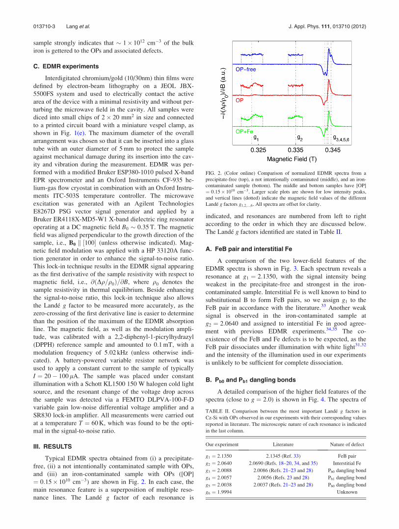
Typical EDMR spectra obtained from (i) a precipitate-free, (ii) a not intentionally contaminated sample with OPs,and (iii) an iron-contaminated sample with OPs ([OP]$ 0:15" 1010 cm#3) are shown in Fig. 2. In each case, themain resonance feature is a superposition of multiple reso-nance lines. The Lande g factor of each resonance is
indicated, and resonances are numbered from left to rightaccording to the order in which they are discussed below.The Lande g factors identified are stated in Table II.
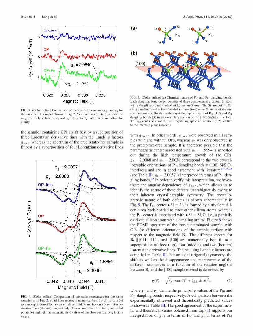
A. FeB pair and interstitial Fe
A comparison of the two lower-field features of theEDMR spectra is shown in Fig. 3. Each spectrum reveals aresonance at g1 $ 2:1350, with the signal intensity beingweakest in the precipitate-free and strongest in the iron-contaminated sample. Interstitial Fe is well known to bind tosubstitutional B to form FeB pairs, so we assign g1 to theFeB pair in accordance with the literature.33 Another weaksignal is observed in the iron-contaminated sample atg2 $ 2:0640 and assigned to interstitial Fe in good agree-ment with previous EDMR experiments.34,35 The co-existence of the FeB and Fe defects is to be expected, as theFeB pair dissociates under illumination with white light31,32
and the intensity of the illumination used in our experimentsis unlikely to be sufficient for complete dissociation.
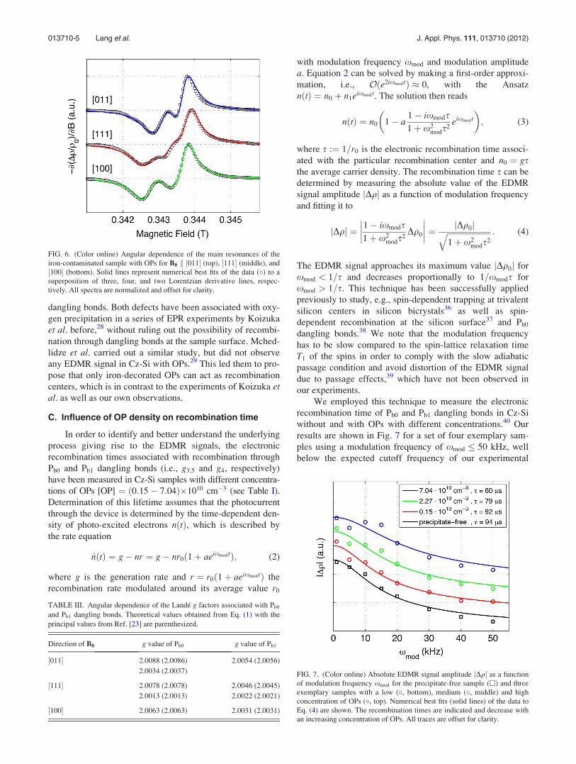
B. Pb0 and Pb1 dangling bonds
A detailed comparison of the higher field features of thespectra (close to g $ 2:0) is shown in Fig. 4. The spectra of
FIG. 2. (Color online) Comparison of normalized EDMR spectra from aprecipitate-free (top), a not intentionally contaminated (middle), and an iron-contaminated sample (bottom). The middle and bottom samples have [OP]$ 0:15" 1010 cm#3. Larger scale plots are shown for low intensity peaks,and vertical lines (dotted) indicate the magnetic field values of the differentLande g factors g1;2;:::;6. All spectra are offset for clarity.
TABLE II. Comparison between the most important Lande g factors inCz-Si with OPs observed in our experiments with their corresponding valuesreported in literature. The microscopic nature of each resonance is indicated
in the last column.
Our experiment Literature Nature of defect
g1 $ 2:1350 2.1345 (Ref. 33) FeB pair
g2 $ 2:0640 2.0690 (Refs. 18–20, 34, and 35) Interstitial Fe
g3 $ 2:0088 2.0086 (Refs. 21–23 and 28) Pb0 dangling bond
g4 $ 2:0057 2.0056 (Refs. 23 and 28) Pb1 dangling bond
g5 $ 2:0038 2.0037 (Refs. 21–23 and 28) Pb0 dangling bond
g6 $ 1:9994 Unknown
013710-3 Lang et al. J. Appl. Phys. 111, 013710 (2012)
the samples containing OPs are fit best by a superposition ofthree Lorentzian derivative lines with the Lande g factorsg3;4;5, whereas the spectrum of the precipitate-free sample isfit best by a superposition of four Lorentzian derivative lines
with g3;4;5;6. In other words, g3;4;5 were observed in all sam-ples with and without OPs, whereas g6 was only observed inthe precipitate-free sample. It is therefore possible that theparamagnetic center associated with g6 $ 1:9994 is annealedout during the high temperature growth of the OPs.g3 $ 2:0088 and g5 $ 2:0038 correspond to the two crystal-lographic orientations of Pb0 dangling bonds at (100) Si/SiO2
interfaces and are in good agreement with literature21–23,28
(see Table II). g4 $ 2:0057 is interpreted in terms of Pb1 dan-gling bonds.23 In order to verify this interpretation, we inves-tigate the angular dependence of g3;4;5, which allows us toidentify the nature of these defects, unambiguously owing totheir inherent crystallographic symmetry. The crystallo-graphic nature of both defects is shown schematically inFig. 5. The Pb0 center * Si + Si3 is formed by a trivalent sili-con atom back-bonded to three other silicon atoms, whereasthe Pb1 center is associated with *Si + Si2O, i.e., a partiallyoxidized silicon atom with a dangling orbital. Figure 6 showsthe EDMR spectrum of the iron-contaminated sample, withOPs for different orientations of the sample surface withrespect to the magnetic field B0. The different spectra forB0 k (011); (111); and (100) are numerically best fit to asuperposition of three (top), four (middle), and two (bottom)Lorentzian derivative lines. The resulting Lande g factors arecompiled in Table III. For an axial (trigonal) symmetry, theshift as well as the disappearance and reappearance of thedifferent resonances as a function of the rotation angle hbetween B0 and the (100) sample normal is described by
g%h& $!!!!!!!!!!!!!!!!!!!!!!!!!!!!!!!!!!!!!!!!!!!!!!!%gjj cos h&2 , %g? sin h&2
q; (1)
where gjj and g? denote the principal g values of the Pb0 andPb1 dangling bonds, respectively. A comparison between theexperimentally observed and theoretically predicted valuesis shown in Table III. The good agreement of the experimen-tal and theoretical values obtained from Eq. (1) supports ourinterpretation of g3;5 in terms of Pb0 and g4 in terms of Pb1
FIG. 3. (Color online) Comparison of the low-field resonances g1 and g2 forthe same set of samples shown in Fig. 2. Vertical lines (dotted) indicate themagnetic field values of g1 and g2, respectively. All traces are offset forclarity.
FIG. 4. (Color online) Comparison of the main resonances for the samesamples as in Fig. 2. Solid lines represent numerical best fits of the data (')to a superposition of four (top) and three (middle and bottom) Lorentzian de-rivative lines (dashed), respectively. Traces are offset for clarity and solidpoints (*) highlight the magnetic field values of the observed Lande g factorsg3;4;5;6.
FIG. 5. (Color online) (a) Chemical nature of Pb0 and Pb1 dangling bonds.Each dangling bond defect consists of three components: a central Si atomwith a dangling orbital (dashed stick) and an O atom. The Si atom of the Pb0(Pb1) dangling bond is back-bonded to three (two) other Si atoms of the sur-rounding matrix. (b) shows the crystallographic nature of Pb0 (1,2) and Pb1dangling bonds (3) in an exemplary section of the (100) Si/SiO2 interface.The Pb0 center has two different crystallographic orientations (1,2) relativeto the interface plane (shaded).
013710-4 Lang et al. J. Appl. Phys. 111, 013710 (2012)
dangling bonds. Both defects have been associated with oxy-gen precipitation in a series of EPR experiments by Koizukaet al. before,28 without ruling out the possibility of recombi-nation through dangling bonds at the sample surface. Mched-lidze et al. carried out a similar study, but did not observeany EDMR signal in Cz-Si with OPs.29 This led them to pro-pose that only iron-decorated OPs can act as recombinationcenters, which is in contrast to the experiments of Koizuka etal. as well as our own observations.
C. Influence of OP density on recombination time
In order to identify and better understand the underlyingprocess giving rise to the EDMR signals, the electronicrecombination times associated with recombination throughPb0 and Pb1 dangling bonds (i.e., g3;5 and g4, respectively)have been measured in Cz-Si samples with different concentra-tions of OPs [OP] $ %0:15# 7:04&"1010 cm#3 (see Table I).Determination of this lifetime assumes that the photocurrentthrough the device is determined by the time-dependent den-sity of photo-excited electrons n%t&, which is described bythe rate equation
_n%t& $ g# nr $ g# nr0%1, aeixmodt&; (2)
where g is the generation rate and r $ r0%1, aeixmodt& therecombination rate modulated around its average value r0
with modulation frequency xmod and modulation amplitudea. Equation 2 can be solved by making a first-order approxi-mation, i.e., O%e2ixmodt& - 0, with the Ansatzn%t& $ n0 , n1eixmodt. The solution then reads
n%t& $ n0 1# a1# ixmods1, x2
mods2eixmodt
" #; (3)
where s :$ 1=r0 is the electronic recombination time associ-ated with the particular recombination center and n0 $ gsthe average carrier density. The recombination time s can bedetermined by measuring the absolute value of the EDMRsignal amplitude jDqj as a function of modulation frequencyand fitting it to
jDqj $ 1# ixmods1, x2
mods2Dq0
$$$$
$$$$ $jDq0j!!!!!!!!!!!!!!!!!!!!!!
1, x2mods2
q : (4)
The EDMR signal approaches its maximum value jDq0j forxmod < 1=s and decreases proportionally to 1=xmods forxmod > 1=s. This technique has been successfully appliedpreviously to study, e.g., spin-dependent trapping at trivalentsilicon centers in silicon bicrystals36 as well as spin-dependent recombination at the silicon surface37 and Pb0dangling bonds.38 We note that the modulation frequencyhas to be slow compared to the spin-lattice relaxation timeT1 of the spins in order to comply with the slow adiabaticpassage condition and avoid distortion of the EDMR signaldue to passage effects,39 which have not been observed inour experiments.
We employed this technique to measure the electronicrecombination time of Pb0 and Pb1 dangling bonds in Cz-Siwithout and with OPs with different concentrations.40 Ourresults are shown in Fig. 7 for a set of four exemplary sam-ples using a modulation frequency of xmod . 50 kHz, wellbelow the expected cutoff frequency of our experimental
TABLE III. Angular dependence of the Lande g factors associated with Pb0and Pb1 dangling bonds. Theoretical values obtained from Eq. (1) with theprincipal values from Ref. [23] are parenthesized.
Direction of B0 g value of Pb0 g value of Pb1
(011) 2.0088 (2.0086) 2.0054 (2.0056)
2.0034 (2.0037)
(111) 2.0078 (2.0078) 2.0046 (2.0045)
2.0013 (2.0013) 2.0022 (2.0021)
(100) 2.0063 (2.0063) 2.0031 (2.0031)
FIG. 6. (Color online) Angular dependence of the main resonances of theiron-contaminated sample with OPs for B0 k (011) (top), (111) (middle), and(100) (bottom). Solid lines represent numerical best fits of the data (') to asuperposition of three, four, and two Lorentzian derivative lines, respec-tively. All spectra are normalized and offset for clarity.
FIG. 7. (Color online) Absolute EDMR signal amplitude jDqj as a functionof modulation frequency xmod for the precipitate-free sample (h) and threeexemplary samples with a low (', bottom), medium (', middle) and highconcentration of OPs (', top). Numerical best fits (solid lines) of the data toEq. (4) are shown. The recombination times are indicated and decrease withan increasing concentration of OPs. All traces are offset for clarity.
013710-5 Lang et al. J. Appl. Phys. 111, 013710 (2012)
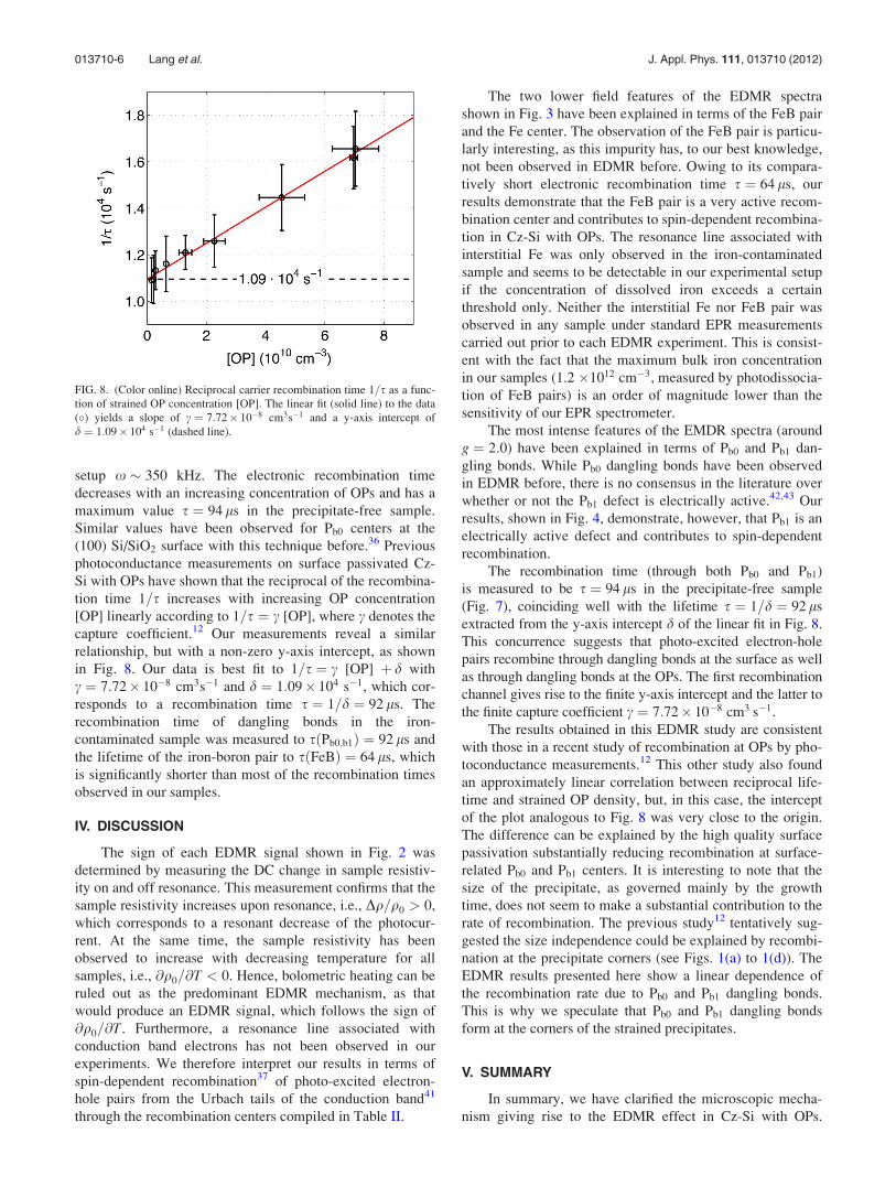
setup x ! 350 kHz. The electronic recombination timedecreases with an increasing concentration of OPs and has amaximum value s $ 94 ls in the precipitate-free sample.Similar values have been observed for Pb0 centers at the(100) Si/SiO2 surface with this technique before.36 Previousphotoconductance measurements on surface passivated Cz-Si with OPs have shown that the reciprocal of the recombina-tion time 1=s increases with increasing OP concentration[OP] linearly according to 1=s $ c [OP], where c denotes thecapture coefficient.12 Our measurements reveal a similarrelationship, but with a non-zero y-axis intercept, as shownin Fig. 8. Our data is best fit to 1=s $ c [OP] , d withc $ 7:72" 10#8 cm3s#1 and d $ 1:09" 104 s#1, which cor-responds to a recombination time s $ 1=d $ 92 ls. Therecombination time of dangling bonds in the iron-contaminated sample was measured to s%Pb0;b1& $ 92 ls andthe lifetime of the iron-boron pair to s%FeB& $ 64 ls, whichis significantly shorter than most of the recombination timesobserved in our samples.
IV. DISCUSSION
The sign of each EDMR signal shown in Fig. 2 wasdetermined by measuring the DC change in sample resistiv-ity on and off resonance. This measurement confirms that thesample resistivity increases upon resonance, i.e., Dq=q0 > 0,which corresponds to a resonant decrease of the photocur-rent. At the same time, the sample resistivity has beenobserved to increase with decreasing temperature for allsamples, i.e., @q0=@T < 0. Hence, bolometric heating can beruled out as the predominant EDMR mechanism, as thatwould produce an EDMR signal, which follows the sign of@q0=@T. Furthermore, a resonance line associated withconduction band electrons has not been observed in ourexperiments. We therefore interpret our results in terms ofspin-dependent recombination37 of photo-excited electron-hole pairs from the Urbach tails of the conduction band41
through the recombination centers compiled in Table II.
The two lower field features of the EDMR spectrashown in Fig. 3 have been explained in terms of the FeB pairand the Fe center. The observation of the FeB pair is particu-larly interesting, as this impurity has, to our best knowledge,not been observed in EDMR before. Owing to its compara-tively short electronic recombination time s $ 64 ls, ourresults demonstrate that the FeB pair is a very active recom-bination center and contributes to spin-dependent recombina-tion in Cz-Si with OPs. The resonance line associated withinterstitial Fe was only observed in the iron-contaminatedsample and seems to be detectable in our experimental setupif the concentration of dissolved iron exceeds a certainthreshold only. Neither the interstitial Fe nor FeB pair wasobserved in any sample under standard EPR measurementscarried out prior to each EDMR experiment. This is consist-ent with the fact that the maximum bulk iron concentrationin our samples (1.2 "1012 cm#3, measured by photodissocia-tion of FeB pairs) is an order of magnitude lower than thesensitivity of our EPR spectrometer.
The most intense features of the EMDR spectra (aroundg $ 2:0) have been explained in terms of Pb0 and Pb1 dan-gling bonds. While Pb0 dangling bonds have been observedin EDMR before, there is no consensus in the literature overwhether or not the Pb1 defect is electrically active.42,43 Ourresults, shown in Fig. 4, demonstrate, however, that Pb1 is anelectrically active defect and contributes to spin-dependentrecombination.
The recombination time (through both Pb0 and Pb1)is measured to be s $ 94 ls in the precipitate-free sample(Fig. 7), coinciding well with the lifetime s $ 1=d $ 92 lsextracted from the y-axis intercept d of the linear fit in Fig. 8.This concurrence suggests that photo-excited electron-holepairs recombine through dangling bonds at the surface as wellas through dangling bonds at the OPs. The first recombinationchannel gives rise to the finite y-axis intercept and the latter tothe finite capture coefficient c $ 7:72" 10#8 cm3 s#1.
The results obtained in this EDMR study are consistentwith those in a recent study of recombination at OPs by pho-toconductance measurements.12 This other study also foundan approximately linear correlation between reciprocal life-time and strained OP density, but, in this case, the interceptof the plot analogous to Fig. 8 was very close to the origin.The difference can be explained by the high quality surfacepassivation substantially reducing recombination at surface-related Pb0 and Pb1 centers. It is interesting to note that thesize of the precipitate, as governed mainly by the growthtime, does not seem to make a substantial contribution to therate of recombination. The previous study12 tentatively sug-gested the size independence could be explained by recombi-nation at the precipitate corners (see Figs. 1(a) to 1(d)). TheEDMR results presented here show a linear dependence ofthe recombination rate due to Pb0 and Pb1 dangling bonds.This is why we speculate that Pb0 and Pb1 dangling bondsform at the corners of the strained precipitates.
V. SUMMARY
In summary, we have clarified the microscopic mecha-nism giving rise to the EDMR effect in Cz-Si with OPs.
FIG. 8. (Color online) Reciprocal carrier recombination time 1=s as a func-tion of strained OP concentration [OP]. The linear fit (solid line) to the data(') yields a slope of c $ 7:72" 10#8 cm3s#1 and a y-axis intercept ofd $ 1:09" 104 s#1 (dashed line).
013710-6 Lang et al. J. Appl. Phys. 111, 013710 (2012)
Spin-dependent recombination of photo-excited electron-hole pairs has been identified as the predominant EDMRmechanism. We observe two coexisting defect configura-tions of dissolved iron (interstitial Fe and FeB) and showthat both of them do contribute to spin-dependent recombi-nation. We have demonstrated that both the electronicrecombination time and the capture coefficient can be meas-ured with EDMR by changing the modulation frequency.Our recombination time analysis on precipitate-free and on aseries of precipitate containing samples with different con-centrations of OPs has shown, in particular, that photo-excited electron-hole pairs recombine through Pb0 and Pb1dangling bonds formed at the sample surface and OPs. Therecombination rate associated with OPs was found toincrease approximately linearly with an increasing density ofstrained OPs with the capture coefficient c $ 7:72" 10#8
cm3s#1. Further insight into the recombination process andits dynamics may be obtained from pulsed-44 and high-fieldEDMR45 experiments, which will allow us to determine anycoupling between the different centers and to study spin-dependent recombination with an enhanced spectral resolu-tion, respectively.
ACKNOWLEDGMENTS
The authors thank D. Gambaro, M. Cornara, and M.Olmo of MEMC Electronic Materials Inc. for performingprecipitation treatments and characterization and V.Y.Resnik at the Institute of Rare Metals (Moscow) for perform-ing TEM analyses. We also thank H. Hubl for fruitful discus-sions and acknowledge funding from Konrad-Adenauer-Stiftung e.V., EPSRC DTA, and Trinity College Oxford.J.D.M. is supported by the Royal Academy of Engineering,EPSRC, and St. Anne’s College Oxford, and J.J.L.M. by TheRoyal Society and St. John’s College Oxford.
1A. Borghesi, B. Pivac, A. Sassella, and A. Stella, J. Appl. Phys. 77, 4169(1995).
2R. C. Newman, J. Phys.: Condens. Matter 12, R335 (2000).3T. Y. Tan, E. E. Gardner, and W. K. Tice, Appl. Phys. Lett. 30, 175(1977).
4S. M. Myers, M. Seibt, and W. Schroter, J. Appl. Phys. 88, 3795 (2000).5D. Gilles, E. R. Weber, and S. Hahn, Phys. Rev. Lett. 64, 196 (1990).6A. Giannattasio, J. D. Murphy, S. Sendaker, R. J. Falster, and P. R. Wil-shaw, J. Electrochem. Soc. 152, G460 (2005).
7K. Jurkschat, S. Senkader, P. R. Wilshaw, D. Gambaro, and R. J. Falster,J. Appl. Phys. 90, 3219 (2001).
8C. S. Fuller and R. A. Logan, J. Appl. Phys. 28, 1427 (1957).9H. Fischer and W. Pschunder, Proc. of the 10th IEEE PVSC, Palo Alto,CA, 13–15 November 1973, p. 404.
10K. Bothe and J. Schmidt, J. Appl. Phys. 99, 013701 (2006).11J. Vanhellemont, E. Simoen, A. Kaniava, M. Libzeny, and C. Claeys,J. Appl. Phys. 77, 5669 (1995).
12J. D. Murphy, K. Bothe, M. Olmo, V. V. Voronkov, and R. J. Falster,J. Appl. Phys. 110, 053713 (2011).
13K. Bothe, K. Ramspeck, D. Hinken, C. Schinke, J. Schmidt, S. Herlufsen,R. Brendel, J. Bauer, J.-M. Wagner, N. Zakharov, and O. Breitenstein,J. Appl. Phys. 106, 104510 (2009).
14L. Chen, X. Yu, P. Chen, P. Wang, X. Gu, J. Lu, and D. Yang, Sol. EnergyMater. Sol. Cells 95, 3148 (2011).
15R. Falster, V. V. Voronkov, V. Y. Resnik, and M. G. Milvidskii, High Pu-rity Silicon VIII: Proceedings of the International Symposium, edited byC. L. Claeys, M. Watanabe, R. Falster, and P. Stallhofer (The Electro-chemical Society, Pennington, NJ, 2004) Vol. 5, p. 188.
16W. Bergholz, M. J. Binns, G. R. Booker, J. C. Hutchison, S. H. Kinder, S.Messoloras, R. C. Newman, R. J. Stewart, and J. G. Wilkes, Philos. Mag.B 59, 499 (1989).
17R. A. Sinton and A. Cuevas, Appl. Phys. Lett. 69, 2510 (1996).18H. H. Woodbury and G. W. Ludwig, Phys. Rev. 117, 102 (1960).19Y. H. Lee, R. L. Kleinhenz, and J. W. Corbett, Appl. Phys. Lett. 31, 142(1977).
20E. H. Poindexter and P. J. Caplan, Prog. Surf. Sci. 14, 201 (1983).21W. E. Carlos, Appl. Phys. Lett. 50, 1450 (1987).22K. L. Brower, Z. Phys. Chem. 151, 177 (1987).23A. Stesmans and V. V. Afanas’ev, J. Appl. Phys. 83, 2449 (1998).24C. Boehme and K. Lips, Physica B 376–377, 930 (2006).25D. R. McCamey, H. Huebl, M. S. Brandt, W. D. Hutchison, J. C. McCal-lum, R. G. Clark, and A. R. Hamilton, Appl. Phys. Lett. 89, 182115(2006).
26C. C. Lo, V. Lang, R. E. George, J. J. L. Morton, A. M. Tyryshkin, S.A. Lyon, J. Bokor, and T. Schenkel, Phys. Rev. Lett. 106, 207601(2011).
27M. Stutzmann, M. S. Brandt, and M. W. Bayerl, J. Non-Cryst. Solids266–269, 1 (2000).
28M. Koizuka and H. Yamada-Kaneta, J. Appl. Phys. 88, 1784 (2000).29T. Mchedlidze and K. Matsumoto, J. Appl. Phys. 83, 4042 (1998).30K. F. Kelton, R. Falster, D. Gambaro, M. Olmo, M. Cornara, and P. F.Wei, J. Appl. Phys. 85, 8097 (1999).
31G. Zoth and W. Bergholz, J. Appl. Phys. 67, 6764 (1990).32J. D. Murphy and R. J. Falster, Phys. Status Solidi (RRL) 5, 370 (2011).33A. A. Istratov, H. Hieslmair, and E. R. Weber, Appl. Phys. A 69, 13(1999).
34W. Gehlhoff, N. T. Bagraev, and L. E. Klyachkin, Mater. Sci. Forum 196,467 (1995).
35W. Gehlhoff and K. H. Segsa, Phys. Status Solidi B 115, 443 (1983).36P. M. Lenahan and W. K. Schubert, Phys. Rev. B 30, 1544 (1984).37D. J. Lepine, Phys. Rev. B 6, 436 (1972).38P. M. Lenahan and M. A. Jupina, Colloids Surf. 45, 191 (1990).39M. Weger, Bell Syst. Tech. J. 39, 1013 (1960), available at: http://www.alcatel-lucent.com/bstj/vol39-1960/articles/bstj39-4-1013.pdf.
40We defined the EDMR signal amplitude Dqj j as the difference betweenthe absolute maximum and minimum of the dangling bond resonance(Fig. 4). The electronic recombination time s thus corresponds to the totalrecombination time of charge carriers through Pb0 and Pb1 dangling bonds.We have also measured the recombination time of the Pb0 and Pb1 centerseparately by extracting the different contributions to the dangling bondresonance and their individual recombination times according to Eq. 4.This measurement revealed the same recombination time for both Pb0 andPb1 dangling bonds.
41F. Urbach, Phys. Rev. 92, 1324 (1953).42A. Stesmans and V. V. Afanas’ev, Phys. Rev. B 57, 10030 (1998).43T. D. Mishima, P. M. Lenahan, and W. Weber, Appl. Phys. Lett. 76, 3771(2000).
44C. Boehme and K. Lips, Phys. Rev. B 68, 245105 (2003).45V. Lang, C. C. Lo, R. E. George, S. A. Lyon, J. Bokor, T. Schenkel, A.Ardavan, and J. J. L. Morton, Rev. Sci. Instrum. 82, 034704 (2011).
013710-7 Lang et al. J. Appl. Phys. 111, 013710 (2012)