spi serial communication and nokia 5110 lcd screen · the nokia screen has a pin named data/command...
TRANSCRIPT

Lab 5 Rev 0.1 Synchronous Serial Communication
- 1 -
5.1 Objectives:
Many devices use Serial Communication to communicate with each other. The advantage of serial communication is that it uses relatively few lines to send large amounts of data. Serial communication can come in many forms, I2C, SPI, UART, just to name a few. This lab will demonstrate how to use SPI interface to control the Nokia 5110 LCD screen. In this lab, you will learn,
• How to setup the SSI peripheral of Tiva.
• How to send data using the SPI interface.
• How to setup the Nokia 5110 LCD display.
• How to display images and characters on the LCD screen.
• How to debug serial communication using a logic analyzer.
Related material to read:
• Chapter 22 in text, but only for basic concepts.
• TM4C123GH6PM Data Sheet, Chapters 14 and 15.
• Nokia 5110 Data Sheet
SPI Serial Communication and Nokia 5110 LCD Screen
5
Lab 5 Rev 0.1 Synchronous Serial Communication
- 2 -
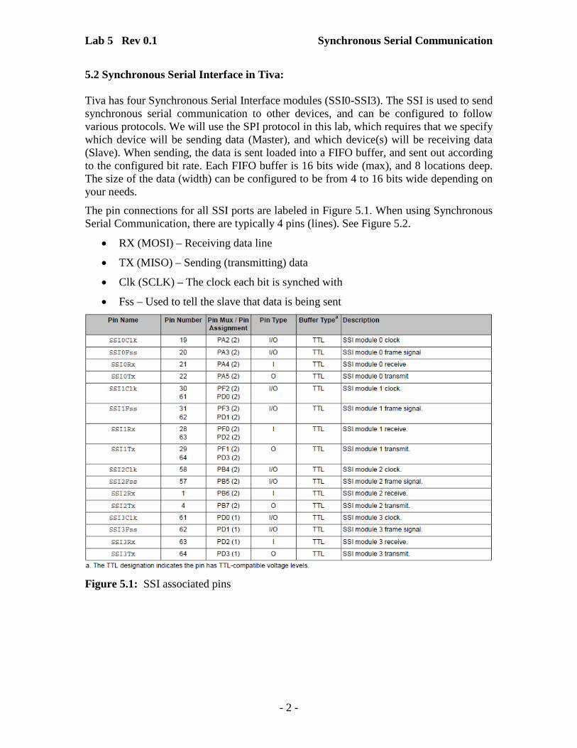
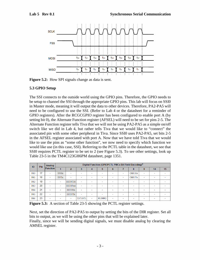
5.2 Synchronous Serial Interface in Tiva: Tiva has four Synchronous Serial Interface modules (SSI0-SSI3). The SSI is used to send synchronous serial communication to other devices, and can be configured to follow various protocols. We will use the SPI protocol in this lab, which requires that we specify which device will be sending data (Master), and which device(s) will be receiving data (Slave). When sending, the data is sent loaded into a FIFO buffer, and sent out according to the configured bit rate. Each FIFO buffer is 16 bits wide (max), and 8 locations deep. The size of the data (width) can be configured to be from 4 to 16 bits wide depending on your needs. The pin connections for all SSI ports are labeled in Figure 5.1. When using Synchronous Serial Communication, there are typically 4 pins (lines). See Figure 5.2.
• RX (MOSI) – Receiving data line
• TX (MISO) – Sending (transmitting) data
• Clk (SCLK) – The clock each bit is synched with
• Fss – Used to tell the slave that data is being sent
Figure 5.1: SSI associated pins
Lab 5 Rev 0.1 Synchronous Serial Communication
- 3 -
Figure 5.2: How SPI signals change as data is sent.
5.3 GPIO Setup
The SSI connects to the outside world using the GPIO pins. Therefore, the GPIO needs to be setup to channel the SSI through the appropriate GPIO pins. This lab will focus on SSI0 in Master mode, meaning it will output the data to other devices. Therefore, PA2-PA5 will need to be configured to use the SSI. (Refer to Lab 4 or the datasheet for a reminder of GPIO registers). After the RCGCGPIO register has been configured to enable port A (by setting bit 0), the Alternate Function register (AFSEL) will need to be set for pins 2-5. The Alternate Function register tells Tiva that we will not be using PA2-PA5 as a simple on/off switch like we did in Lab 4, but rather tells Tiva that we would like to “connect” the associated pin with some other peripheral in Tiva. Since SSI0 uses PA2-PA5, set bits 2-5 in the AFSEL register associated with port A. Now that we have told Tiva that we would like to use the pins as “some other function”, we now need to specify which function we would like use (in this case, SSI). Referring to the PCTL table in the datasheet, we see that SSI0 requires PCTL register to be set to 2 (see Figure 5.3). To see other settings, look up Table 23-5 in the TM4C123GH6PM datasheet, page 1351.
Figure 5.3: A section of Table 23-5 showing the PCTL register settings.
Next, set the direction of PA2-PA5 to output by setting the bits of the DIR register. Set all bits to output, as we will be using the other pins that will be explained later. Finally, since we will be sending digital signals, we must disable analog by clearing the AMSEL register.
Lab 5 Rev 0.1 Synchronous Serial Communication
- 4 -
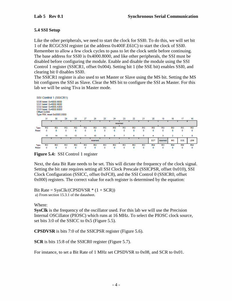
5.4 SSI Setup Like the other peripherals, we need to start the clock for SSI0. To do this, we will set bit 1 of the RCGCSSI register (at the address 0x400F.E61C) to start the clock of SSI0. Remember to allow a few clock cycles to pass to let the clock settle before continuing. The base address for SSI0 is 0x4000.8000, and like other peripherals, the SSI must be disabled before configuring the module. Enable and disable the module using the SSI Control 1 register (SSICR1, offset 0x004). Setting bit 1 (the SSE bit) enables SSI0, and clearing bit 0 disables SSI0. The SSICR1 register is also used to set Master or Slave using the MS bit. Setting the MS bit configures the SSI as Slave. Clear the MS bit to configure the SSI as Master. For this lab we will be using Tiva in Master mode.
Figure 5.4: SSI Control 1 register
Next, the data Bit Rate needs to be set. This will dictate the frequency of the clock signal. Setting the bit rate requires setting all SSI Clock Prescale (SSICPSR, offset 0x010), SSI Clock Configuration (SSICC, offset 0xFC8), and the SSI Control 0 (SSICR0, offset 0x000) registers. The correct value for each register is determined by the equation: Bit Rate = SysClk/(CPSDVSR * (1 + SCR)) a) From section 15.3.1 of the datasheet. Where: SysClk is the frequency of the oscillator used. For this lab we will use the Precision Internal OSCillator (PIOSC) which runs at 16 MHz. To select the PIOSC clock source, set bits 3:0 of the SSICC to 0x5 (Figure 5.5). CPSDVSR is bits 7:0 of the SSICPSR register (Figure 5.6). SCR is bits 15:8 of the SSICR0 register (Figure 5.7). For instance, to set a Bit Rate of 1 MHz set CPSDVSR to 0x08, and SCR to 0x01.

Lab 5 Rev 0.1 Synchronous Serial Communication
- 5 -
Figure 5.5: SSI Clock Configuration
Figure 5.6: SSI Clock Prescale register
Figure 5.7: SSI Control 0 register
Next, the size of the data being sent needs to be specified. This is done using the DSS bits of the SSICR0 register (Figure 5.7). The SSI supports data sizes 4 bits to 16 bits. The DSS bits follow the equation DSS = Data Size -1. Meaning to select a data size of 4 bits, set DSS to 0x03. Similarly, to select a data size of 16 bits, set DSS to 0x0F.
Lab 5 Rev 0.1 Synchronous Serial Communication
- 6 -
Finally, the Frame Format needs to be specified. The Frame Format sets timings on when the FSS logic flips, and the data is sent, among other things. The devices you are trying to interface with should specify these timings, so you will choose one that works for your application. For this lab, we will use the Freescale SPI frame format. To select the Freescale SPI frame format, clear bits 5:4 of the SSICR0 register.
After all registers have been configured, you can enable the SSI using the SSICR1 register.
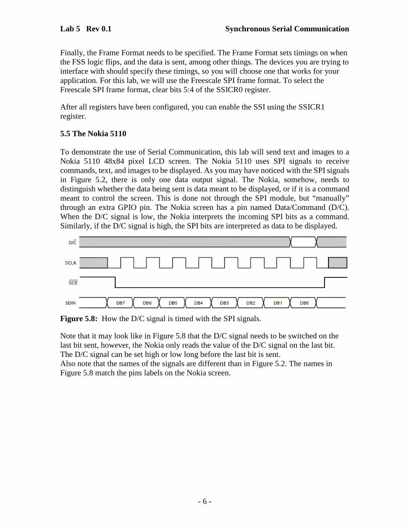
5.5 The Nokia 5110 To demonstrate the use of Serial Communication, this lab will send text and images to a Nokia 5110 48x84 pixel LCD screen. The Nokia 5110 uses SPI signals to receive commands, text, and images to be displayed. As you may have noticed with the SPI signals in Figure 5.2, there is only one data output signal. The Nokia, somehow, needs to distinguish whether the data being sent is data meant to be displayed, or if it is a command meant to control the screen. This is done not through the SPI module, but “manually” through an extra GPIO pin. The Nokia screen has a pin named Data/Command (D/C). When the D/C signal is low, the Nokia interprets the incoming SPI bits as a command. Similarly, if the D/C signal is high, the SPI bits are interpreted as data to be displayed.
Figure 5.8: How the D/C signal is timed with the SPI signals.
Note that it may look like in Figure 5.8 that the D/C signal needs to be switched on the last bit sent, however, the Nokia only reads the value of the D/C signal on the last bit. The D/C signal can be set high or low long before the last bit is sent. Also note that the names of the signals are different than in Figure 5.2. The names in Figure 5.8 match the pins labels on the Nokia screen.
Lab 5 Rev 0.1 Synchronous Serial Communication
- 7 -
Connecting the Nokia Screen Signal Nokia Tiva Board
Power Vcc (Pin 1) 3.3V Ground GND (Pin 2) GND FSS SCE (Pin 3) PA3 Reset RST (Pin 4) PA7 Data/Command D/C (pin 5) PA6 MISO (TX) DN (Pin 6) PA5 Clock SCLK (Pin 7) PA2 Back Light LED (Pin 8) (Resistor)*
Table 9.1: Signal connections between Tiva and the Nokia screen. *Note the back lighting LED’s need to have their current limited to ~80mA 5.5.1 Testing your connections To help you ensure that you connected your Nokia screen correctly, we have included the file “NCT.hex” to download to your board. If your screen is connected correctly, you will see “Hello from Nokia” displayed on your screen. After a couple of seconds, the character V will be displayed repeatedly. This gives a perfect opportunity to view the signals using a logic analyzer (explained below). A hex file is already compiled code containing the actual ones and zeros the processor executes. The process for downloading this file is different than what you are used to. To download a hex file to your board:
1. Start a new project and select the appropriate processor and debugger. 2. Save the hex file in the Objects folder inside the project directory. 3. In the Options for Target window (Project-> Options for Target) choose the Output
tab and enter the name of the hex file into the “Name of Executable” text box. 4. You are now able to click the Download icon and hit the reset button on the board.
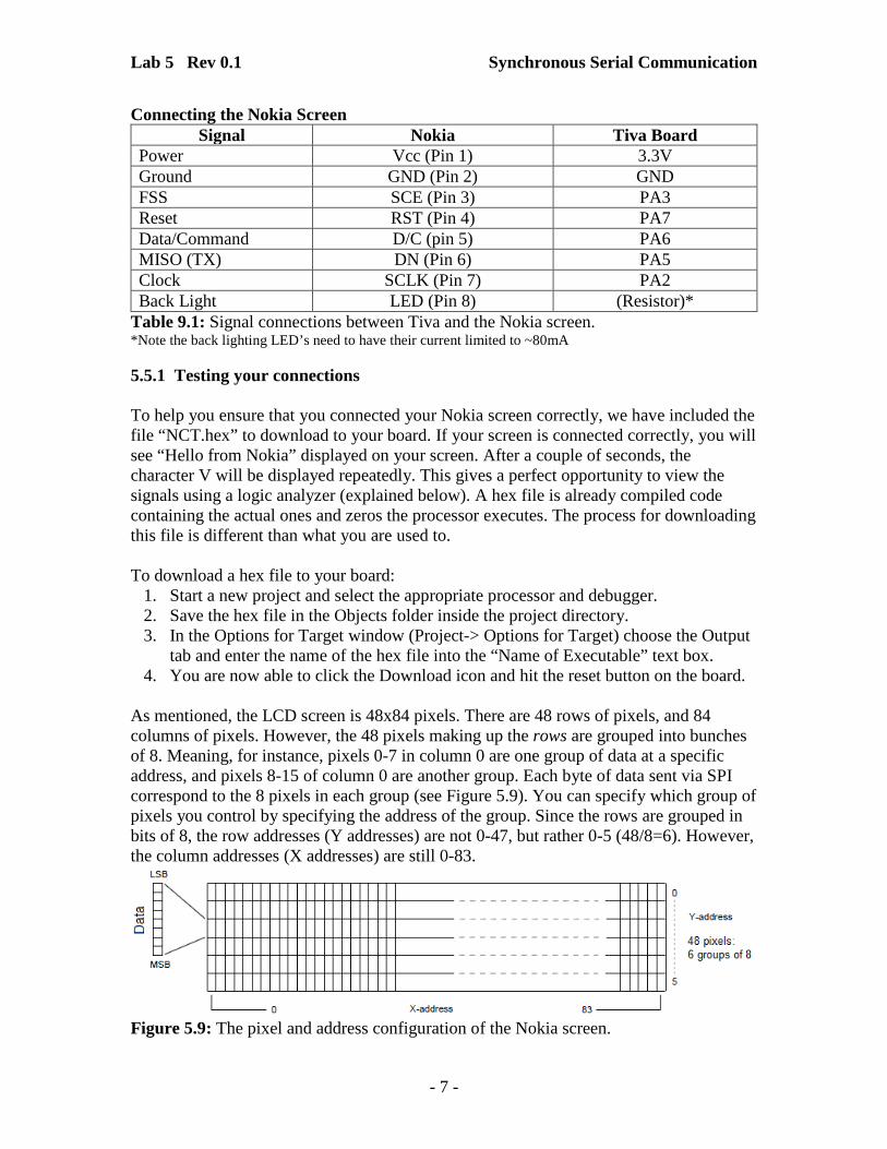
As mentioned, the LCD screen is 48x84 pixels. There are 48 rows of pixels, and 84 columns of pixels. However, the 48 pixels making up the rows are grouped into bunches of 8. Meaning, for instance, pixels 0-7 in column 0 are one group of data at a specific address, and pixels 8-15 of column 0 are another group. Each byte of data sent via SPI correspond to the 8 pixels in each group (see Figure 5.9). You can specify which group of pixels you control by specifying the address of the group. Since the rows are grouped in bits of 8, the row addresses (Y addresses) are not 0-47, but rather 0-5 (48/8=6). However, the column addresses (X addresses) are still 0-83.
Figure 5.9: The pixel and address configuration of the Nokia screen.

Lab 5 Rev 0.1 Synchronous Serial Communication
- 8 -
Displaying any image is simply a matter of stepping through the addresses and sending a byte of data that turns on the correct pixels at each address. Thankfully, the Nokia board makes this even easier on you since the address automatically indexes the column address after every byte sent. Therefore, all that is needed is a stream of data to display. Sending text is just like an image, but typically one character is 8 pixels by 6 pixels. This means the screen can hold 14 characters across and 6 characters down. (See Table 6 in the Nokia 5110 datasheet for good examples).
If you wanted to display the character “P”: Send 0x1F to the first column to turn on all of the pixels in the first column. (Note 0x1F because, in this example, the character is only 5 pixels high) The address automatically indexes to the next column, so there is no need to change the address. Simply send the next byte of data. In this case 0x05. Finally, send 0x07 to finish the character
Since the column address (X address) automatically increments, it is easy to quickly send one byte after another. However, with a BR of only 4 MHz and with the processor running at 16 MHz, the processor can easily fill the SSI FIFO buffer faster than the SSI can empty it. Therefore, you must monitor the SSI Transmit FIFO Not Full (TNF) bit in the SSI Status register (SSISR, offset 0x00C). When the FIFO is NOT full, the TNF bit is a 1. Similarly, the processor is fast enough to move on to other instructions before the SSI is done transmitting. This is the most devastating when switching between Commands and Data. If you were sending a series of commands to the Nokia with the D/C bit low, and then switch to send data to display by setting the D/C bit high, the processor will switch the D/C bit high before the SSI is done sending commands. Therefore, you must monitor the SSI Busy bit (BSY) of the SSI Status register. When the SSI is busy sending data, the BSY bit is a 1.
Figure 5.10: SSI Status register.
Lab 5 Rev 0.1 Synchronous Serial Communication
- 9 -
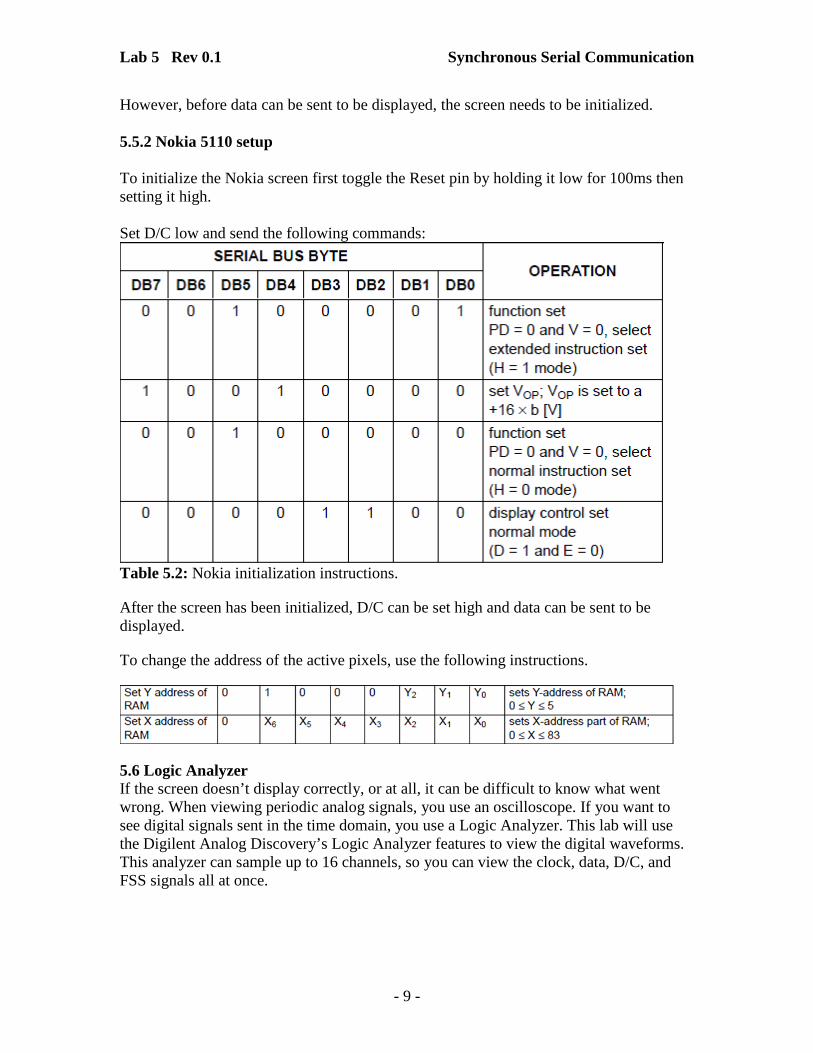
However, before data can be sent to be displayed, the screen needs to be initialized. 5.5.2 Nokia 5110 setup To initialize the Nokia screen first toggle the Reset pin by holding it low for 100ms then setting it high. Set D/C low and send the following commands:
Table 5.2: Nokia initialization instructions.
After the screen has been initialized, D/C can be set high and data can be sent to be displayed.
To change the address of the active pixels, use the following instructions.
5.6 Logic Analyzer If the screen doesn’t display correctly, or at all, it can be difficult to know what went wrong. When viewing periodic analog signals, you use an oscilloscope. If you want to see digital signals sent in the time domain, you use a Logic Analyzer. This lab will use the Digilent Analog Discovery’s Logic Analyzer features to view the digital waveforms. This analyzer can sample up to 16 channels, so you can view the clock, data, D/C, and FSS signals all at once.
Lab 5 Rev 0.1 Synchronous Serial Communication
- 10 -
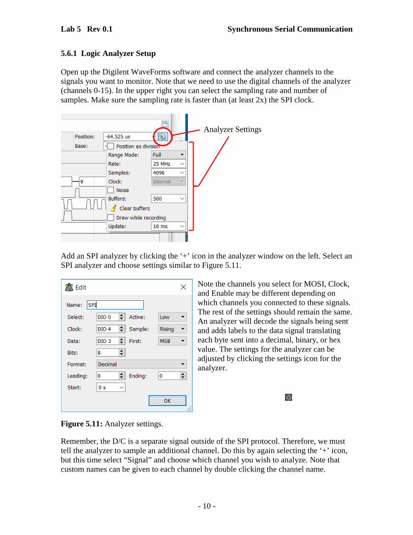
5.6.1 Logic Analyzer Setup Open up the Digilent WaveForms software and connect the analyzer channels to the signals you want to monitor. Note that we need to use the digital channels of the analyzer (channels 0-15). In the upper right you can select the sampling rate and number of samples. Make sure the sampling rate is faster than (at least 2x) the SPI clock.
Add an SPI analyzer by clicking the ‘+’ icon in the analyzer window on the left. Select an SPI analyzer and choose settings similar to Figure 5.11.
Note the channels you select for MOSI, Clock, and Enable may be different depending on which channels you connected to these signals. The rest of the settings should remain the same. An analyzer will decode the signals being sent and adds labels to the data signal translating each byte sent into a decimal, binary, or hex value. The settings for the analyzer can be adjusted by clicking the settings icon for the analyzer.
Figure 5.11: Analyzer settings.
Remember, the D/C is a separate signal outside of the SPI protocol. Therefore, we must tell the analyzer to sample an additional channel. Do this by again selecting the ‘+’ icon, but this time select “Signal” and choose which channel you wish to analyze. Note that custom names can be given to each channel by double clicking the channel name.
Analyzer Settings
Lab 5 Rev 0.1 Synchronous Serial Communication
- 11 -
5.6.2 Using the Logic Analyzer
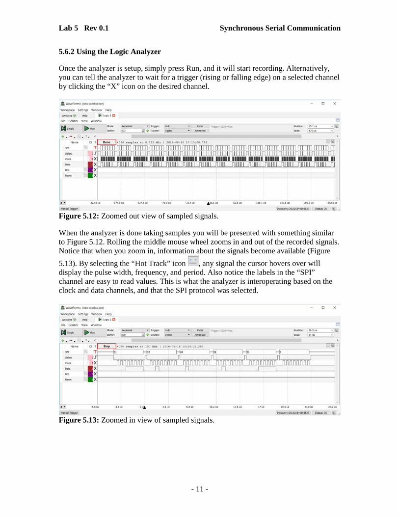
Once the analyzer is setup, simply press Run, and it will start recording. Alternatively, you can tell the analyzer to wait for a trigger (rising or falling edge) on a selected channel by clicking the “X” icon on the desired channel.
Figure 5.12: Zoomed out view of sampled signals.
When the analyzer is done taking samples you will be presented with something similar to Figure 5.12. Rolling the middle mouse wheel zooms in and out of the recorded signals. Notice that when you zoom in, information about the signals become available (Figure 5.13). By selecting the “Hot Track” icon , any signal the cursor hovers over will display the pulse width, frequency, and period. Also notice the labels in the “SPI” channel are easy to read values. This is what the analyzer is interoperating based on the clock and data channels, and that the SPI protocol was selected.
Figure 5.13: Zoomed in view of sampled signals.
Lab 5 Rev 0.1 Synchronous Serial Communication
- 12 -
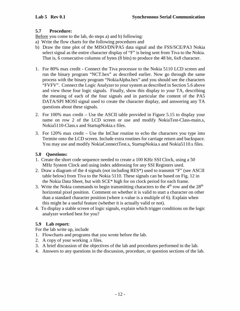
5.7 Procedure: Before you come to the lab, do steps a) and b) following: a) Write the flow charts for the following procedures and b) Draw the time plot of the MISO/DN/PA5 data signal and the FSS/SCE/PA3 Nokia
select signal as the entire character display of “F” is being sent from Tiva to the Nokia. That is, 6 consecutive columns of bytes (8 bits) to produce the 48 bit, 6x8 character.
1. For 80% max credit - Connect the Tiva processor to the Nokia 5110 LCD screen and
run the binary program “NCT.hex” as described earlier. Now go through the same process with the binary program “NokiaAlpha.hex” and you should see the characters “FVFV”. Connect the Logic Analyzer to your system as described in Section 5.6 above and view those four logic signals. Finally, show this display to your TA, describing the meaning of each of the four signals and in particular the content of the PA5 DATA/SPI MOSI signal used to create the character display, and answering any TA questions about these signals.
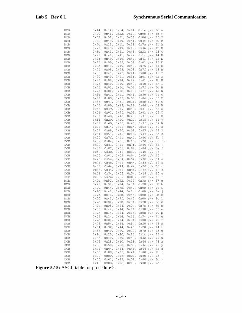
2. For 100% max credit – Use the ASCII table provided in Figure 5.15 to display your name on row 2 of the LCD screen or use and modify NokiaTest-Class-main.s, Nokia5110-Class.s and StartupNokia.s files.
3. For 120% max credit – Use the InChar routine to echo the characters you type into Termite onto the LCD screen. Include extra routines for carriage return and backspace. You may use and modify NokiaConnectTest.s, StartupNokia.s and Nokia5110.s files.
5.8 Questions: 1. Create the short code sequence needed to create a 100 KHz SSI Clock, using a 50
MHz System Clock and using index addressing for any SSI Registers used. 2. Draw a diagram of the 4 signals (not including RES*) used to transmit “F” (see ASCII
table below) from Tiva to the Nokia 5110. These signals can be based on Fig. 12 in the Nokia Data Sheet, but with SCE* high for on clock period for each frame.
3. Write the Nokia commands to begin transmitting characters to the 4th row and the 28th horizontal pixel position. Comment on whether it is valid to start a character on other than a standard character position (where x-value is a multiple of 6). Explain when this might be a useful feature (whether it is actually valid or not).
4. To display a stable screen of logic signals, explain which trigger conditions on the logic analyzer worked best for you?
5.9 Lab report: For the lab write up, include 1. Flowcharts and programs that you wrote before the lab. 2. A copy of your working .s files. 3. A brief discussion of the objectives of the lab and procedures performed in the lab. 4. Answers to any questions in the discussion, procedure, or question sections of the lab.
Lab 5 Rev 0.1 Synchronous Serial Communication
- 13 -
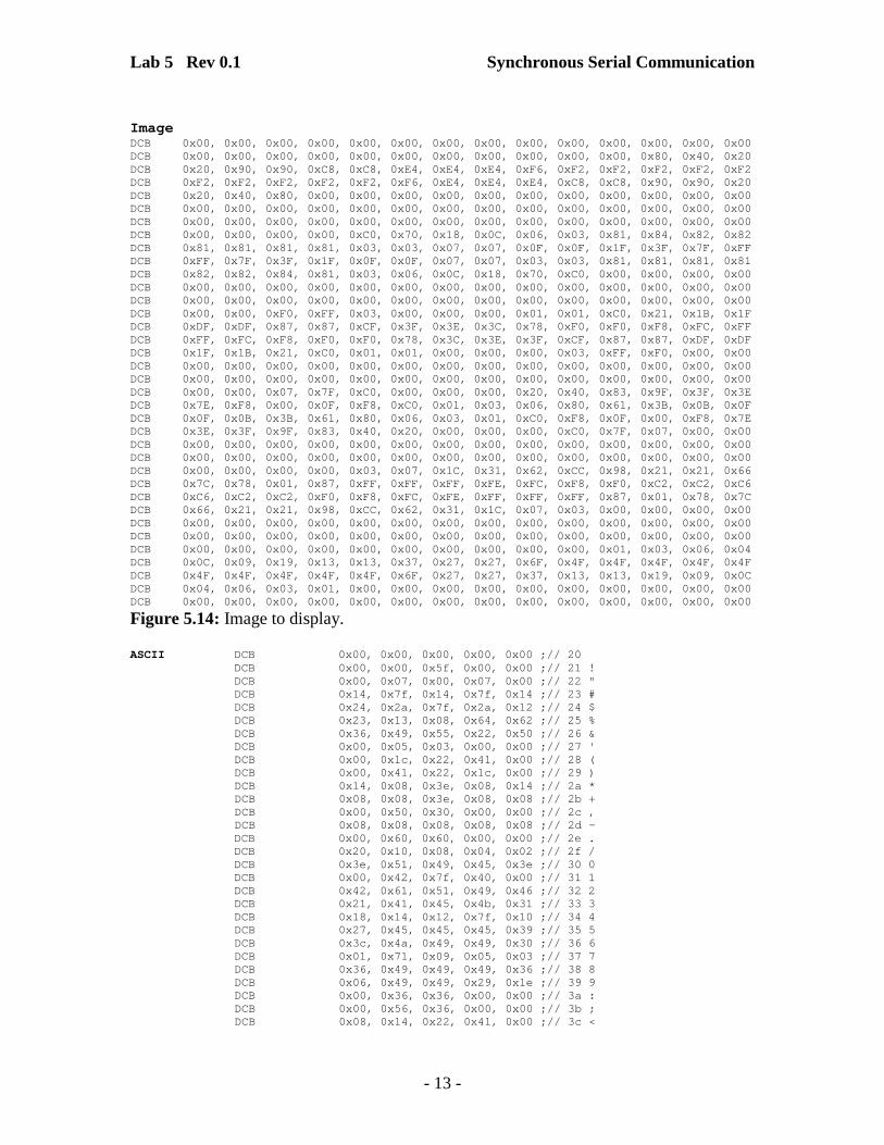
Image DCB 0x00, 0x00, 0x00, 0x00, 0x00, 0x00, 0x00, 0x00, 0x00, 0x00, 0x00, 0x00, 0x00, 0x00 DCB 0x00, 0x00, 0x00, 0x00, 0x00, 0x00, 0x00, 0x00, 0x00, 0x00, 0x00, 0x80, 0x40, 0x20 DCB 0x20, 0x90, 0x90, 0xC8, 0xC8, 0xE4, 0xE4, 0xE4, 0xF6, 0xF2, 0xF2, 0xF2, 0xF2, 0xF2 DCB 0xF2, 0xF2, 0xF2, 0xF2, 0xF2, 0xF6, 0xE4, 0xE4, 0xE4, 0xC8, 0xC8, 0x90, 0x90, 0x20 DCB 0x20, 0x40, 0x80, 0x00, 0x00, 0x00, 0x00, 0x00, 0x00, 0x00, 0x00, 0x00, 0x00, 0x00 DCB 0x00, 0x00, 0x00, 0x00, 0x00, 0x00, 0x00, 0x00, 0x00, 0x00, 0x00, 0x00, 0x00, 0x00 DCB 0x00, 0x00, 0x00, 0x00, 0x00, 0x00, 0x00, 0x00, 0x00, 0x00, 0x00, 0x00, 0x00, 0x00 DCB 0x00, 0x00, 0x00, 0x00, 0xC0, 0x70, 0x18, 0x0C, 0x06, 0x03, 0x81, 0x84, 0x82, 0x82 DCB 0x81, 0x81, 0x81, 0x81, 0x03, 0x03, 0x07, 0x07, 0x0F, 0x0F, 0x1F, 0x3F, 0x7F, 0xFF DCB 0xFF, 0x7F, 0x3F, 0x1F, 0x0F, 0x0F, 0x07, 0x07, 0x03, 0x03, 0x81, 0x81, 0x81, 0x81 DCB 0x82, 0x82, 0x84, 0x81, 0x03, 0x06, 0x0C, 0x18, 0x70, 0xC0, 0x00, 0x00, 0x00, 0x00 DCB 0x00, 0x00, 0x00, 0x00, 0x00, 0x00, 0x00, 0x00, 0x00, 0x00, 0x00, 0x00, 0x00, 0x00 DCB 0x00, 0x00, 0x00, 0x00, 0x00, 0x00, 0x00, 0x00, 0x00, 0x00, 0x00, 0x00, 0x00, 0x00 DCB 0x00, 0x00, 0xF0, 0xFF, 0x03, 0x00, 0x00, 0x00, 0x01, 0x01, 0xC0, 0x21, 0x1B, 0x1F DCB 0xDF, 0xDF, 0x87, 0x87, 0xCF, 0x3F, 0x3E, 0x3C, 0x78, 0xF0, 0xF0, 0xF8, 0xFC, 0xFF DCB 0xFF, 0xFC, 0xF8, 0xF0, 0xF0, 0x78, 0x3C, 0x3E, 0x3F, 0xCF, 0x87, 0x87, 0xDF, 0xDF DCB 0x1F, 0x1B, 0x21, 0xC0, 0x01, 0x01, 0x00, 0x00, 0x00, 0x03, 0xFF, 0xF0, 0x00, 0x00 DCB 0x00, 0x00, 0x00, 0x00, 0x00, 0x00, 0x00, 0x00, 0x00, 0x00, 0x00, 0x00, 0x00, 0x00 DCB 0x00, 0x00, 0x00, 0x00, 0x00, 0x00, 0x00, 0x00, 0x00, 0x00, 0x00, 0x00, 0x00, 0x00 DCB 0x00, 0x00, 0x07, 0x7F, 0xC0, 0x00, 0x00, 0x00, 0x20, 0x40, 0x83, 0x9F, 0x3F, 0x3E DCB 0x7E, 0xF8, 0x00, 0x0F, 0xF8, 0xC0, 0x01, 0x03, 0x06, 0x80, 0x61, 0x3B, 0x0B, 0x0F DCB 0x0F, 0x0B, 0x3B, 0x61, 0x80, 0x06, 0x03, 0x01, 0xC0, 0xF8, 0x0F, 0x00, 0xF8, 0x7E DCB 0x3E, 0x3F, 0x9F, 0x83, 0x40, 0x20, 0x00, 0x00, 0x00, 0xC0, 0x7F, 0x07, 0x00, 0x00 DCB 0x00, 0x00, 0x00, 0x00, 0x00, 0x00, 0x00, 0x00, 0x00, 0x00, 0x00, 0x00, 0x00, 0x00 DCB 0x00, 0x00, 0x00, 0x00, 0x00, 0x00, 0x00, 0x00, 0x00, 0x00, 0x00, 0x00, 0x00, 0x00 DCB 0x00, 0x00, 0x00, 0x00, 0x03, 0x07, 0x1C, 0x31, 0x62, 0xCC, 0x98, 0x21, 0x21, 0x66 DCB 0x7C, 0x78, 0x01, 0x87, 0xFF, 0xFF, 0xFF, 0xFE, 0xFC, 0xF8, 0xF0, 0xC2, 0xC2, 0xC6 DCB 0xC6, 0xC2, 0xC2, 0xF0, 0xF8, 0xFC, 0xFE, 0xFF, 0xFF, 0xFF, 0x87, 0x01, 0x78, 0x7C DCB 0x66, 0x21, 0x21, 0x98, 0xCC, 0x62, 0x31, 0x1C, 0x07, 0x03, 0x00, 0x00, 0x00, 0x00 DCB 0x00, 0x00, 0x00, 0x00, 0x00, 0x00, 0x00, 0x00, 0x00, 0x00, 0x00, 0x00, 0x00, 0x00 DCB 0x00, 0x00, 0x00, 0x00, 0x00, 0x00, 0x00, 0x00, 0x00, 0x00, 0x00, 0x00, 0x00, 0x00 DCB 0x00, 0x00, 0x00, 0x00, 0x00, 0x00, 0x00, 0x00, 0x00, 0x00, 0x01, 0x03, 0x06, 0x04 DCB 0x0C, 0x09, 0x19, 0x13, 0x13, 0x37, 0x27, 0x27, 0x6F, 0x4F, 0x4F, 0x4F, 0x4F, 0x4F DCB 0x4F, 0x4F, 0x4F, 0x4F, 0x4F, 0x6F, 0x27, 0x27, 0x37, 0x13, 0x13, 0x19, 0x09, 0x0C DCB 0x04, 0x06, 0x03, 0x01, 0x00, 0x00, 0x00, 0x00, 0x00, 0x00, 0x00, 0x00, 0x00, 0x00 DCB 0x00, 0x00, 0x00, 0x00, 0x00, 0x00, 0x00, 0x00, 0x00, 0x00, 0x00, 0x00, 0x00, 0x00
Figure 5.14: Image to display. ASCII DCB 0x00, 0x00, 0x00, 0x00, 0x00 ;// 20 DCB 0x00, 0x00, 0x5f, 0x00, 0x00 ;// 21 ! DCB 0x00, 0x07, 0x00, 0x07, 0x00 ;// 22 " DCB 0x14, 0x7f, 0x14, 0x7f, 0x14 ;// 23 # DCB 0x24, 0x2a, 0x7f, 0x2a, 0x12 ;// 24 $ DCB 0x23, 0x13, 0x08, 0x64, 0x62 ;// 25 % DCB 0x36, 0x49, 0x55, 0x22, 0x50 ;// 26 & DCB 0x00, 0x05, 0x03, 0x00, 0x00 ;// 27 ' DCB 0x00, 0x1c, 0x22, 0x41, 0x00 ;// 28 ( DCB 0x00, 0x41, 0x22, 0x1c, 0x00 ;// 29 ) DCB 0x14, 0x08, 0x3e, 0x08, 0x14 ;// 2a * DCB 0x08, 0x08, 0x3e, 0x08, 0x08 ;// 2b + DCB 0x00, 0x50, 0x30, 0x00, 0x00 ;// 2c , DCB 0x08, 0x08, 0x08, 0x08, 0x08 ;// 2d - DCB 0x00, 0x60, 0x60, 0x00, 0x00 ;// 2e . DCB 0x20, 0x10, 0x08, 0x04, 0x02 ;// 2f / DCB 0x3e, 0x51, 0x49, 0x45, 0x3e ;// 30 0 DCB 0x00, 0x42, 0x7f, 0x40, 0x00 ;// 31 1 DCB 0x42, 0x61, 0x51, 0x49, 0x46 ;// 32 2 DCB 0x21, 0x41, 0x45, 0x4b, 0x31 ;// 33 3 DCB 0x18, 0x14, 0x12, 0x7f, 0x10 ;// 34 4 DCB 0x27, 0x45, 0x45, 0x45, 0x39 ;// 35 5 DCB 0x3c, 0x4a, 0x49, 0x49, 0x30 ;// 36 6 DCB 0x01, 0x71, 0x09, 0x05, 0x03 ;// 37 7 DCB 0x36, 0x49, 0x49, 0x49, 0x36 ;// 38 8 DCB 0x06, 0x49, 0x49, 0x29, 0x1e ;// 39 9 DCB 0x00, 0x36, 0x36, 0x00, 0x00 ;// 3a : DCB 0x00, 0x56, 0x36, 0x00, 0x00 ;// 3b ; DCB 0x08, 0x14, 0x22, 0x41, 0x00 ;// 3c <
Lab 5 Rev 0.1 Synchronous Serial Communication
- 14 -
DCB 0x14, 0x14, 0x14, 0x14, 0x14 ;// 3d = DCB 0x00, 0x41, 0x22, 0x14, 0x08 ;// 3e > DCB 0x02, 0x01, 0x51, 0x09, 0x06 ;// 3f ? DCB 0x32, 0x49, 0x79, 0x41, 0x3e ;// 40 @ DCB 0x7e, 0x11, 0x11, 0x11, 0x7e ;// 41 A DCB 0x7f, 0x49, 0x49, 0x49, 0x36 ;// 42 B DCB 0x3e, 0x41, 0x41, 0x41, 0x22 ;// 43 C DCB 0x7f, 0x41, 0x41, 0x22, 0x1c ;// 44 D DCB 0x7f, 0x49, 0x49, 0x49, 0x41 ;// 45 E DCB 0x7f, 0x09, 0x09, 0x09, 0x01 ;// 46 F DCB 0x3e, 0x41, 0x49, 0x49, 0x7a ;// 47 G DCB 0x7f, 0x08, 0x08, 0x08, 0x7f ;// 48 H DCB 0x00, 0x41, 0x7f, 0x41, 0x00 ;// 49 I DCB 0x20, 0x40, 0x41, 0x3f, 0x01 ;// 4a J DCB 0x7f, 0x08, 0x14, 0x22, 0x41 ;// 4b K DCB 0x7f, 0x40, 0x40, 0x40, 0x40 ;// 4c L DCB 0x7f, 0x02, 0x0c, 0x02, 0x7f ;// 4d M DCB 0x7f, 0x04, 0x08, 0x10, 0x7f ;// 4e N DCB 0x3e, 0x41, 0x41, 0x41, 0x3e ;// 4f O DCB 0x7f, 0x09, 0x09, 0x09, 0x06 ;// 50 P DCB 0x3e, 0x41, 0x51, 0x21, 0x5e ;// 51 Q DCB 0x7f, 0x09, 0x19, 0x29, 0x46 ;// 52 R DCB 0x46, 0x49, 0x49, 0x49, 0x31 ;// 53 S DCB 0x01, 0x01, 0x7f, 0x01, 0x01 ;// 54 T DCB 0x3f, 0x40, 0x40, 0x40, 0x3f ;// 55 U DCB 0x1f, 0x20, 0x40, 0x20, 0x1f ;// 56 V DCB 0x3f, 0x40, 0x38, 0x40, 0x3f ;// 57 W DCB 0x63, 0x14, 0x08, 0x14, 0x63 ;// 58 X DCB 0x07, 0x08, 0x70, 0x08, 0x07 ;// 59 Y DCB 0x61, 0x51, 0x49, 0x45, 0x43 ;// 5a Z DCB 0x00, 0x7f, 0x41, 0x41, 0x00 ;// 5b [ DCB 0x02, 0x04, 0x08, 0x10, 0x20 ;// 5c '\' DCB 0x00, 0x41, 0x41, 0x7f, 0x00 ;// 5d ] DCB 0x04, 0x02, 0x01, 0x02, 0x04 ;// 5e ^ DCB 0x40, 0x40, 0x40, 0x40, 0x40 ;// 5f _ DCB 0x00, 0x01, 0x02, 0x04, 0x00 ;// 60 ` DCB 0x20, 0x54, 0x54, 0x54, 0x78 ;// 61 a DCB 0x7f, 0x48, 0x44, 0x44, 0x38 ;// 62 b DCB 0x38, 0x44, 0x44, 0x44, 0x20 ;// 63 c DCB 0x38, 0x44, 0x44, 0x48, 0x7f ;// 64 d DCB 0x38, 0x54, 0x54, 0x54, 0x18 ;// 65 e DCB 0x08, 0x7e, 0x09, 0x01, 0x02 ;// 66 f DCB 0x0c, 0x52, 0x52, 0x52, 0x3e ;// 67 g DCB 0x7f, 0x08, 0x04, 0x04, 0x78 ;// 68 h DCB 0x00, 0x44, 0x7d, 0x40, 0x00 ;// 69 i DCB 0x20, 0x40, 0x44, 0x3d, 0x00 ;// 6a j DCB 0x7f, 0x10, 0x28, 0x44, 0x00 ;// 6b k DCB 0x00, 0x41, 0x7f, 0x40, 0x00 ;// 6c l DCB 0x7c, 0x04, 0x18, 0x04, 0x78 ;// 6d m DCB 0x7c, 0x08, 0x04, 0x04, 0x78 ;// 6e n DCB 0x38, 0x44, 0x44, 0x44, 0x38 ;// 6f o DCB 0x7c, 0x14, 0x14, 0x14, 0x08 ;// 70 p DCB 0x08, 0x14, 0x14, 0x18, 0x7c ;// 71 q DCB 0x7c, 0x08, 0x04, 0x04, 0x08 ;// 72 r DCB 0x48, 0x54, 0x54, 0x54, 0x20 ;// 73 s DCB 0x04, 0x3f, 0x44, 0x40, 0x20 ;// 74 t DCB 0x3c, 0x40, 0x40, 0x20, 0x7c ;// 75 u DCB 0x1c, 0x20, 0x40, 0x20, 0x1c ;// 76 v DCB 0x3c, 0x40, 0x30, 0x40, 0x3c ;// 77 w DCB 0x44, 0x28, 0x10, 0x28, 0x44 ;// 78 x DCB 0x0c, 0x50, 0x50, 0x50, 0x3c ;// 79 y DCB 0x44, 0x64, 0x54, 0x4c, 0x44 ;// 7a z DCB 0x00, 0x08, 0x36, 0x41, 0x00 ;// 7b { DCB 0x00, 0x00, 0x7f, 0x00, 0x00 ;// 7c | DCB 0x00, 0x41, 0x36, 0x08, 0x00 ;// 7d } DCB 0x10, 0x08, 0x08, 0x10, 0x08 ;// 7e ~
Figure 5.15: ASCII table for procedure 2.