specification for liquid crystal display
TRANSCRIPT

JE-AN
ELEC
TR
ON
ICS C
O.,
LTD
S
PEC
IFIC
ATIO
NS F
OR
LIQ
UID
CRYSTAL D
ISPLAY M
AD
E IN
KO
REA
SPECIFICATION FOR LIQUID CRYSTAL DISPLAY
Model No. : JA-SGB1286411 Date : 2006.02.07
Approved Checked Department
Customer :
Model No. : Date :
Approved Checked Department
HEAD OFFICE : 535-127 , KASAN-DONG , KUMCHON-KU , SEOUL , KOREA
TEL : +82-2-857-6515 FAX : +82-2-857-6517
E-MAIL : [email protected] [email protected] [email protected]
DATE 2006.02.07 CUSTOMER MODEL JA-SGB1286411
PART LCD MODULE JE-AN Electronics Co., Ltd COUNTRY KOREA

JE-AN
ELEC
TR
ON
ICS C
O.,
LTD
S
PEC
IFIC
ATIO
NS F
OR
LIQ
UID
CRYSTAL D
ISPLAY M
AD
E IN
KO
REA
1. Features --------------------------------------------------- (2)
2. Mechanical Specifications --------------------------------- (2)
3. Electrical Specifications ----------------------------------- (2-3)
4. Power Supply ---------------------------------------- (4)
5. Electro-optical Characteristics ---------------------------- (5)
6. Terminal Functions and Block Diagram --------------------- (6)
7. Timing Characteristics ------------------------------------ (7)
8. Unit Driving Method ------------------------------------ (8-15)
9. Measuring Method and Equipment ----------------------- (16-18)
10. Standard Specifications for Product Quality ------------------ (19-21)
11. Temperature Range & Relative Humidity -------------------- (22)
12. Engineering Drawing -------------------------------------- (23)
13. Application Notes ----------------------------------------- (24)
PART LCD PANEL JE-AN Electronics Co., Ltd Page 1
Content

JE-AN
ELEC
TR
ON
ICS C
O.,
LTD
S
PEC
IFIC
ATIO
NS F
OR
LIQ
UID
CRYSTAL D
ISPLAY M
AD
E IN
KO
REA
1. FEATURES
The features of LCD Module are as follows :
* Display Model : STN, Negative type, Blue
* Color : Display Dot :white
* Display format : 128 Dots x 64 Dots
* Interface Input Data : 8 bit
* Driving Method : 1/64 Duty , 1/9 Bias
* Viewing Direction : 6 O'clock
2. MECHANICAL SPECIFICATIONS
No. Item Specification Unit
1 Module Size 75 x 52.5 x 9.4(MAX) mm
2 Number of Dots 128 x 64
3 Viewing Area 59 x 31.5 mm
4 Effective Display Area 55 x 27.5 mm
5 Dot Size 0.4 x 0.4 mm
6 Dot Pitch 0.43 x 0.43 mm
7 Weight About 41 g
3. ELECTRICAL SPECIFICATIONS
3-1. ABSOLUTE MAXIMUM RATINGS (Ta=25。C)
No. Item SymbolStandard Value
UnitMin Type Max
1 Supply Voltage For Logic VDD-Vss 0 - 6 V
2 Supply Voltage For LCD Drive VDD-V0 8 - 12 V
3 Input Voltage VI Vss - VDD V
4 Operating Voltage Temp. Top -10 - 50 ˚C
5 Storage Voltage Temp. Tst -20 - 60 ˚C
6 Humidy - - - 90 %RH
PART LCD MODULE JE-AN Electronics Co., Ltd Page 2
JE-AN
ELEC
TR
ON
ICS C
O.,
LTD
S
PEC
IFIC
ATIO
NS F
OR
LIQ
UID
CRYSTAL D
ISPLAY M
AD
E IN
KO
REA
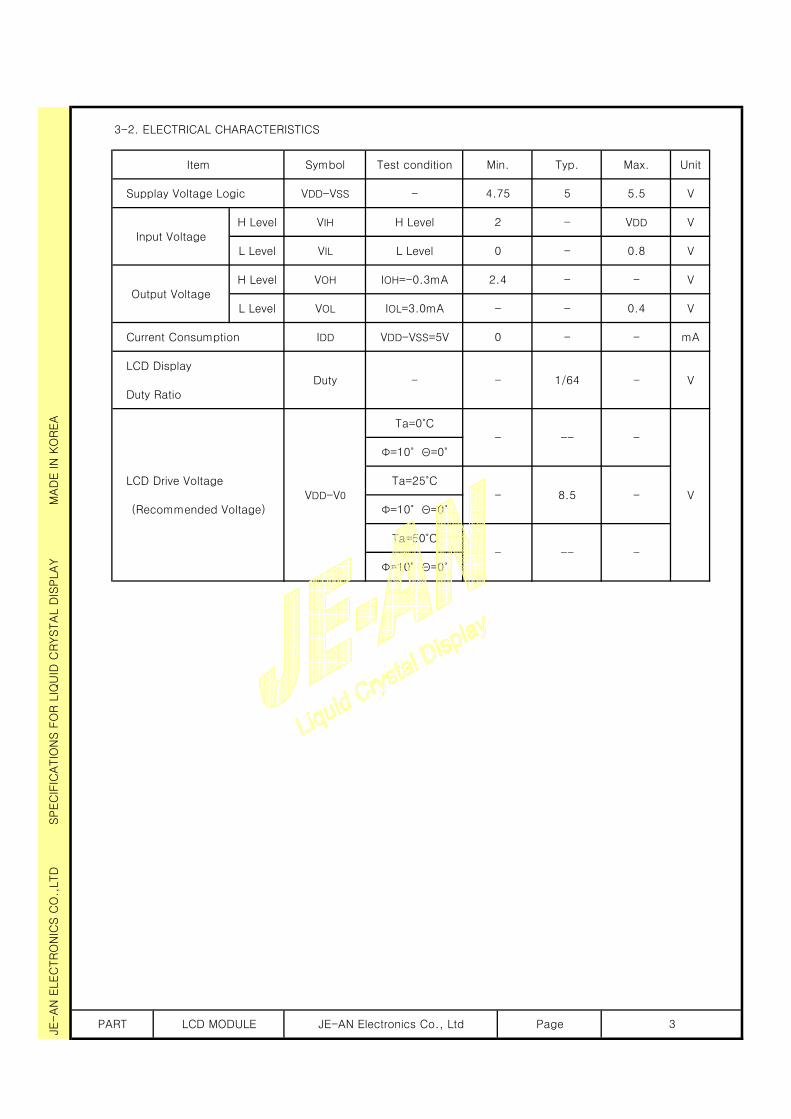
3-2. ELECTRICAL CHARACTERISTICS
Item Symbol Test condition Min. Typ. Max. Unit
Supplay Voltage Logic VDD-VSS - 4.75 5 5.5 V
Input VoltageH Level VIH H Level 2 - VDD V
L Level VIL L Level 0 - 0.8 V
Output VoltageH Level VOH IOH=-0.3mA 2.4 - - V
L Level VOL IOL=3.0mA - - 0.4 V
Current Consumption IDD VDD-VSS=5V 0 - - mA
LCD DisplayDuty - - 1/64 - V
Duty Ratio
VDD-V0
Ta=0˚C- -- -
V
Φ=10˚ Θ=0˚
LCD Drive Voltage Ta=25˚C- 8.5 -
(Recommended Voltage) Φ=10˚ Θ=0˚
Ta=50˚C- -- -
Φ=10˚ Θ=0˚
PART LCD MODULE JE-AN Electronics Co., Ltd Page 3

JE-AN
ELEC
TR
ON
ICS C
O.,
LTD
S
PEC
IFIC
ATIO
NS F
OR
LIQ
UID
CRYSTAL D
ISPLAY M
AD
E IN
KO
REA
4. POWER SUPPLY
VDD
VDD (5V)
VSS
LCDVDD
MODULE
V0 VR
VOUT
* VDD-V0=Operating Voltage for LCD
* VR : About 20k
PART LCD MODULE JE-AN Electronics Co., Ltd Page 4

JE-AN
ELEC
TR
ON
ICS C
O.,
LTD
S
PEC
IFIC
ATIO
NS F
OR
LIQ
UID
CRYSTAL D
ISPLAY M
AD
E IN
KO
REA
5. ELECTRO-OPTICAL CHARACTERISTICS
(Ta=25˚C VDD-V0=10.5V)
Item Symbol Min. Typ. Max. Unit Condition Note
Viewing Θ1-Θ2 30- - deg. Cr=2.0 1,2
Angle Φ 80
ContrastCr - 4 - -
Θ=20˚3
Ratio Φ=0˚
ResponseTr - 250 - ms
Θ=20˚4
Time(rise) Φ=0˚
ResponseTf - 250 - ms
Θ=20˚4
Time(fall) Φ=0˚
Note 1. Definition of Angle Θ & Φ Note 2. Definition of viewing Angle Θ1 & Θ2
Note 3. Definition of Contrast ratio(Cr) Note 4. Definition of Response Time
PART LCD MODULE JE-AN Electronics Co., Ltd Page 5
Y2=(Φ=180 )
Top
X1
Y2=(Φ=0 )
X2
θ1θ2
θ1
2
Cr
θ220
θ1< 20° < θ2
Y2=(Φ =0 )
Cr=B/A
SetPoint
DrivingVoltage
0%
Brightness
A
Non-selectedDots
B
SelectedDots
100 %
Brightness
100 %
Tr
90%
Tf Time
OnOff Off
10 %

JE-AN
ELEC
TR
ON
ICS C
O.,
LTD
S
PEC
IFIC
ATIO
NS F
OR
LIQ
UID
CRYSTAL D
ISPLAY M
AD
E IN
KO
REA
6. TERMINAL FUNCTIONS AND BLOCK DIAGRAM
6-1. INTERFACE PIN FUNCTION DESCRIPTION
PIN NO. SYMBOL FUNCTIONS
1 VDD Power supply for logic circuit (+5.0v)
2 Vss Ground
3 V0 Contrast Adjust
4 DB0
Data Bus Line
5 DB1
6 DB2
7 DB3
8 DB4
9 DB5
10 DB6
11 DB7
12 CS1 Chip Selection Signal for IC1
13 CS2 Chip Selcetion Signal IC2
14 RST Reset (Active " Low")
15 R/W H : Data Read(LCD to MPU) L : Data Write(MPU to LCM)
16 RS H : Data input L : Instruction Code Input
17 E Enable
18 VOUT Output Voltage for LCD Driving
19 A Power for LED backlight (+3.0V/48mA)
20 K Power for LED backlight (-)
6-2. BLOCK DIAGRAM
DB7l SEG 128
DB0 LCD PANEL
ER/W SEGMENT
RS COM V0 DRIVE 64VDDVSS KS0108B x 2
RSTCS1 COMMENT
CS2 DRIVE
VOUT (KS0107B)
PART LCD MODULE JE-AN Electronics Co., Ltd Page 6

JE-AN
ELEC
TR
ON
ICS C
O.,
LTD
S
PEC
IFIC
ATIO
NS F
OR
LIQ
UID
CRYSTAL D
ISPLAY M
AD
E IN
KO
REA
7. TIMING CHARACTERISTICS
Characteristic Symbol Min. Type. Max. Unit
E Cycle Time Tc 1000 - - ns
E Rise Time Tr - - 25 ns
E Fall Time Tf - - 25 ns
E Pulse Width (High, Low) Tw 450 - - ns
Address Setup Time Tasu 140 - - ns
Address Hold Time Tah 10 - - ns
Data Setup time Tsu 200 - - ns
Data Delay Time Td - - 320 ns
Data Hold Time (Write) Tdhw 10 - - ns
Data Hold Time (Read) Tdhr 20 - - ns
PART LCD MODULE JE-AN Electronics Co., Ltd Page 7
CS1-CS2
R/W
DATA
E
t DSU DHWt
2.0V0.8V
AHttASU
2.0V
0.8V
0.8V
2.0V
FtRt
Tw
CT
2.0V
0.8V
D/I
ASUt AHt
Tw
BUS2.0V
2.0V
0.8V
0.8VtASU
0.8V
t DHR
AHt
2.0V
0.8V
Tw
2.0V tASU
TC
t RTw
tF
AHt
MPU W rite tim ing MPU Reading tim ing
Dt

JE-AN
ELEC
TR
ON
ICS C
O.,
LTD
S
PEC
IFIC
ATIO
NS F
OR
LIQ
UID
CRYSTAL D
ISPLAY M
AD
E IN
KO
REA
8. UNIT DRIVING METHOD
8-1. Function of Each Block
Both input register and output register are provided to interface with MPU of which the speed is
different from that of internal operation. The selection of registers depend the combination of R/W
and D/I signals.
Table 1. Register Selection
D/I R/W Operation
1 1Read data out of output register as internal operation
(Display data RAM to output register)
1 0Writes data into register as internal operation
(Inut register to display data RAM)
0 1 Busy check. Read of status data
0 0 Instruction
(1) Input Register
Input register is used to store Data temporarily before writing it info display data RAM.
The data from MPU is written info input register,then into display data RAM automatically
by internal operation.
When chip select signal is in the active mode and D/I and R/W select the Input register
as shown in table 1, data is latched at the fall of "E" signal.
(2) Output Register
The output register is used to store data temporarily that is read from display data RAM.
To read out the data from output register. Chip select signal should be in the active mode
and both D/I and R/W should be "1". With the read instruction, data stored in the output
register is output while "E" is "H" level.
Ten, at the fall of "E", the display data at the indicated address is latched in to the output
register and address is increased by 1. The contents in the output register is rewritten by
read instruction, but are held by address set instruction, ect.
Therefore, the data of the specified address can not be output with read display instrucion,
right after the address is set, but can be output at the second read of data.
That is to say, one dummy read is necessary.
Fig 8-1. Shows the CPU read timming.
PART LCD MODULE JE-AN Electronics Co., Ltd Page 8

JE-AN
ELEC
TR
ON
ICS C
O.,
LTD
S
PEC
IFIC
ATIO
NS F
OR
LIQ
UID
CRYSTAL D
ISPLAY M
AD
E IN
KO
REA
D/I
R/W
E
Address N N+1 N+2
Output register Data at address N Data at address N+1
DB0~DB7 Busy Write Busy Read Busy Read Busy ReadCheck Address Check Data Check Data Check Data
Dummy at atAddress Address
N+1
Fig 8-1. CPU Read Timming
8-1-2. Busy Flag
"1" of busy flag indicates that KS0108B is on the move and any instruction except status read
instruction can not be accepted the value of the busy flag is read out on DB7 by the status
read instruction.
Make sure that the busy flag is reset ("0") before the issue of instruction.
E
Busyflag T busy
4.3 us≤T busy ≤12.9us
8-1-3. Display on/off flag flop
Display on/off flip flop selects one of two state,on state of segments,in on state,the display data
corresponding to that in RAM is output to the segment. On the other hand,the display data at all
segments disappear in off state independent of the data in RAM. It is controlled by display on/off
instruction "0" of RST signal sats the segments in off state,the status of the flip flop is output to
DB5 by status read instruction. Display on/off instruction does not inflence data in RAM.
PART LCD MODULE JE-AN Electronics Co., Ltd Page 9

JE-AN
ELEC
TR
ON
ICS C
O.,
LTD
S
PEC
IFIC
ATIO
NS F
OR
LIQ
UID
CRYSTAL D
ISPLAY M
AD
E IN
KO
REA
8-1-4. Display start register
The register specifies A line in RAM which corresponds to the top line of LCD panel,when
displaying contents in display data RAM on the LCD panel. It is used for scrolling of the screen.
6bit display start line information in this register is transferred to Z address, and the Z address
counter is preset.
8-1-5. X,Y Address counter
This is 9bit counter which designates address of internal display data RAM,X address counter
of upper 3bits and Y address counter of lower 6bits should be set each address by respective
instruction.
(1) X address counter
Ordinary register with no count functions. An address is set in by instruction.
(2) Y address counter
An address is set in by instruction and it is increased by 1 automatically by R/W operations
of display data. The address counter loops the value of 0 to 63 count.
8-1-6. Display data RAM
Dot data for display is stored in this RAM 1 bit data of this RAM corresponds to light on (data=1)
and light off (data=0) of 1 Dot in the display panel.
8-1-7. Reset
The system can initialized by setting RST terminal at "low" level when turning power on.
1) Display off
2) Set display start line register 0 line.
When RST is in low level, any instruction except status read can not be accepted,therefore,
carry out other instruction after making sure that DB4="0" (clear reset) and DB7="0" (ready)
by status read instruction. The conditions of power supply at initial power up are as follows.
PART LCD MODULE JE-AN Electronics Co., Ltd Page 10

JE-AN
ELEC
TR
ON
ICS C
O.,
LTD
S
PEC
IFIC
ATIO
NS F
OR
LIQ
UID
CRYSTAL D
ISPLAY M
AD
E IN
KO
REA
Item Symbol Min. Typ. Max. Unit
Reset time tRST 1.0 - - us
Rise time tr - - 200 us
Do not fail to set the system again because 4.5V
reset during operation may destroy the data VDD
tRSTin all the register except on/off regiser and
0.7 VDD
in RAM.RST 0.3 VDD
tr
8-2. Display control instructions
Table 2 shows the instructions. Read/Write(R/W) signal, data instruction(D/I) signal and data
bus signal (DB0 to DB7) are also called instructions because the internal operation depends
on the signal form MPU generally, there are following three kinds of instructions.
1) Instruction togive address in the internal RAM
2) Instruction to transfer data from / to the internal RAM.
3) Other instructions.
In general use, the instruction "2)" are used most frequently, but,since Y address of the
internal RAM is increased by 1 automatically after writing (reading)data, the program can
be lessened, during the execution of an instruction,the system can not accept other instructions
then status read instruction,send instruction from MPU after marking sure if the busy flag is "0",
which is the proof an instruction is not being executed.
PART LCD MODULE JE-AN Electronics Co., Ltd Page 11

JE-AN
ELEC
TR
ON
ICS C
O.,
LTD
S
PEC
IFIC
ATIO
NS F
OR
LIQ
UID
CRYSTAL D
ISPLAY M
AD
E IN
KO
REA
Table 2
Function
D/I
R/W
DB7
DB6
DB5
DB4
DB3
DB2
DB1
DB0
Description
0 0 0 0 1 1 1 1 1 0/1
Cantrols the on/off displayDisplay
RAM d and internal statuson/off
are not affected. 0:off 1:on
0 0 0 1 Y address (0~63)Set the Y address in the
Set addressY address register.
0 0 1 0 1 1 1 Page(0~7)Set page Set the X address in the
(X address) X address register.
0 0 1 1 Display start line(0~63)
Display start Indicates the display data
line RAM displayed at the top
of the screen.
0 1 BUSY
0 ON/OFF
RESET
0 0 0 0Status Read status :
Read BUSY : 0:Ready
1:In operation
ON/OFF: 0:Display ON
1:Display OFF
RESET : 0:Normal
1:Reset
1 0 Write Data
Write display Write data(DB0~DB7) into
Data display d RAM. After writing
instruction,Y address is
increased by 1 automatically
1 1 Read Data
Read display Reads data(DB0~DB7) into
Data display data RAM to the
data bus.
PART LCD MODULE JE-AN Electronics Co., Ltd Page 12

JE-AN
ELEC
TR
ON
ICS C
O.,
LTD
S
PEC
IFIC
ATIO
NS F
OR
LIQ
UID
CRYSTAL D
ISPLAY M
AD
E IN
KO
REA
8-2-1. Display on/off
R/W D/I DB7 DB6 DB5 DB4 DB3 DB2 DB1 DB0
CODE 0 0 0 0 1 1 1 1 1 D
The display data appears when D is land disappears when D is 0Therought the data is not on the screen width D="0",it rema ins in thedisplay data RAM,therefore,you can make it appear by changingD="0" into D="1"
8-2-2. Display start line
R/W D/I DB7 DB6 DB5 DB4 DB3 DB2 DB1 DB0
CODE 0 0 1 1 A A A A A A
Z address AAAAAA(binary) of the display data RAM is set at the displaystart line register and displayed attech top of the screen fig.8-2 are theexamples of display when the start line=0~3.
COM1 ----- COM1 -----
COM2 ----- COM2 -----
COM3 COM3COM4 COM4COM5 COM5COM6 COM6COM7 COM7COM8 COM8-
-------
-----
--------
-----
----- -----
COM61 COM61COM62 COM62COM63 ----- COM63 -----
COM64 ----- COM64 -----
Start line=0 Start line=1
COM1 ----- COM1 -----
COM2 ----- COM2 -----
COM3 COM3COM4 COM4COM5 COM5COM6 COM6COM7 COM7COM8 COM8-
-------
-----
--------
-----
----- -----
COM61 COM61COM62 COM62COM63 ----- COM63 -----
COM64 ----- COM64 -----
Start line=3 Start line=4
fig 8-2 Relation between start line and display
PART LCD MODULE JE-AN Electronics Co., Ltd Page 13

JE-AN
ELEC
TR
ON
ICS C
O.,
LTD
S
PEC
IFIC
ATIO
NS F
OR
LIQ
UID
CRYSTAL D
ISPLAY M
AD
E IN
KO
REA
8-2-3. Set page (X address)
R/W D/I DB7 DB6 DB5 DB4 DB3 DB2 DB1 DB0
CODE 0 0 1 0 1 1 1 A A A
X address AAA(binary) of the display data RAM is set at theA address register. After that,writing or reading to or from MPUis executed this specified page until the next page is set.
8-2-4. Set page (Y address)
R/W D/I DB7 DB6 DB5 DB4 DB3 DB2 DB1 DB0
CODE 0 0 0 1 A A A A A A
Y address AAAAAA(binary) of the display data RAM is set.the address counter. After that, Y address counter is increased by 1every time the data is written or read to or MPU.
Y address0 1 2 ------- 62 63 0 1 2 ------- 62 63
DB0
page 0
DB0
page 0
----
----
X=0
DB7 DB7DB0
page 1
DB0
page 1
----
----
X=1
DB7 DB7------------
------------
------------
------------
DB0
page 6
- -
DB0
- -
page 6
---
--- X=6
-
DB7
-
DB7DB0
page 7
DB0
page 7
---
--- X=7
-
DB7
-
DB7
IC 1 (CS1 is Active) IC 2 (CS2 is Active)
PART LCD MODULE JE-AN Electronics Co., Ltd Page 14

JE-AN
ELEC
TR
ON
ICS C
O.,
LTD
S
PEC
IFIC
ATIO
NS F
OR
LIQ
UID
CRYSTAL D
ISPLAY M
AD
E IN
KO
REA
8-2-5. Status read
R/W D/I DB7 DB6 DB5 DB4 DB3 DB2 DB1 DB0
CODE 1 0 BUSY 0 ON/OFF RESET 0 0 0 0
BUSY : When "BUSY" is "1". The LSI is in internal operation. No instructions are accepted while busy is "1". So you should make sure that busy is "0" bofore writing the next instruction.
ON/OFF : This bit shows the display conditions. When ON/OFF is "0",the display is in on condition. When ON/OFF is "1",the display is in off condition.
RESET : RESET="1" shows that the system is being initialized. In this condition,any instructions except status read instruction cannot be accepted. RESET="0" shows that initializing has finished and the system is in the usual operation.
8-2-6. Write display data
R/W D/I DB7 DB6 DB5 DB4 DB3 DB2 DB1 DB0
CODE 0 1 A A A A A A A A
Write 8-bit data AAAAAAAA(binary) into the display data RAMthen Y address is increased by 1 automatically.
8-2-7. Read display data
R/W D/I DB7 DB6 DB5 DB4 DB3 DB2 DB1 DB0
CODE 1 1 A A A A A A A A
Read 8-bit data AAAAAAAA(binary) into the display data RAMthen Y address is increased by 1 automatically.One dummy read is necessary soon after the address seting.
PART LCD MODULE JE-AN Electronics Co., Ltd Page 15

JE-AN
ELEC
TR
ON
ICS C
O.,
LTD
S
PEC
IFIC
ATIO
NS F
OR
LIQ
UID
CRYSTAL D
ISPLAY M
AD
E IN
KO
REA
Measuring Method and Equipment
1. Current Consumption Measuring
(1) Equipment
DCPowerSupply
CMOS IC
WaveformGeneratorf=64Hz
A LCD
CB
(2) Condition
Operating Frequency : 64HzOperating Voltage (rms) : Selected Voltage
2. Threshold Voltage and Response Time Measuring
(1) Equipment
L30˚
Oscilloscope
Waveform Generator
PART LCD PANEL JE-AN Electronics Co., Ltd Page 16
㎂

JE-AN
ELEC
TR
ON
ICS C
O.,
LTD
S
PEC
IFIC
ATIO
NS F
OR
LIQ
UID
CRYSTAL D
ISPLAY M
AD
E IN
KO
REA
(2) Definition
a. Threshold Voltage (Vth)
Brightness
100%
80%
Nonselected Waveform
50% Selected Waveform
0 Vset Vth Drive Voltage
b. Response Time
ON
Off
90%
10%Time
tr td
PART LCD PANEL JE-AN Electronics Co., Ltd Page 17

JE-AN
ELEC
TR
ON
ICS C
O.,
LTD
S
PEC
IFIC
ATIO
NS F
OR
LIQ
UID
CRYSTAL D
ISPLAY M
AD
E IN
KO
REA
3. Contrast Measuring
(1) Equipment
L30˚
Oscilloscope
Waveform Generator
(2) Definition
a. Viewing Angle :Z Y 12H,Φ=90˚
Θ1
Θ4 Θ3
9H,Φ=180˚ X 3H,Φ=0˚
Θ2
6H,Φ=2700˚
b. Contrast Ratio (Positive)
Brightness of non-selected wave-formCR =
Brightness of selected wave-form
4. Reliability Test : Equipment : Tenny
PART LCD PANEL JE-AN Electronics Co., Ltd Page 18

JE-AN
ELEC
TR
ON
ICS C
O.,
LTD
S
PEC
IFIC
ATIO
NS F
OR
LIQ
UID
CRYSTAL D
ISPLAY M
AD
E IN
KO
REA
Standard Specifications For Product Quality
1. Manner of Test :
1-1. The test must be under 40W flourescent light, and the distance of view must be at 30cm.
1-2. The test direction is based on around 15˚ -45˚ of Vertical line.
2. Definition of area :
2-1. I area : Viewing area
II area : Outside Viewing area
I
II
2-2. A area : The glass area outside sealant.
G area : Electrode pad area.
F area : Without electrode pad area.
F G G F
A
A
F G G F
3. Definition of defects
3-1. Major defects
a. Non display
b. Segment missing
c. Over current
d. Liquid crystal leakage
f. Wrong polarizer
3-2. Minor defects : The others.
4. Major defects should be in AQL 0.25 , and the Minor in AQL 1.0
PART LCD PANEL JE-AN Electronics Co., Ltd Page 19

JE-AN
ELEC
TR
ON
ICS C
O.,
LTD
S
PEC
IFIC
ATIO
NS F
OR
LIQ
UID
CRYSTAL D
ISPLAY M
AD
E IN
KO
REA
5. Standard of appearance test : (unit : mm)
No. Items CriterionCheckingManner
1
(1) A area YX
Z
X Y Z N
X≤2.0 Y≤0.5 Z≥T/2 N≤3
X≤2.0 Y≤1.0 Z≤T/2 X≤3Substrate crack X≤0.5 Y≤2.0 Z≤T/3 No check
X : Defect Length (2) G area Checking
Z With eyesY : Defect Width
Z : Defect Depth XY
T : Glass ThicknessX Y Z N
N : Defect QTY X≤2.0 Y≤0.5 Z≤T/2 N≤2
L : Connector Width X LY
X Y N≤2
X≤2.0 Y≤1/4 or
X≤2.0 Y≤1.0 N≤2
(3) F area
XY
X Y Z N
X≤2.0 Y≤2 Z≤T N≤3
2
Black spot (1)Y
Checking on the
White spot Table with light
Xdust 0.15<D≤0.2 N≤1 and polarizer ,
0.1<D≤0.15 N≤2Polarizer D≤0.1 No Check and chacking with
(2) LScratch W eyes directly.
D=(X+Y)/2 W NL≤2.0 W ≤0.03 N≤1
PART LCD PANEL JE-AN Electronics Co., Ltd Page 20

JE-AN
ELEC
TR
ON
ICS C
O.,
LTD
S
PEC
IFIC
ATIO
NS F
OR
LIQ
UID
CRYSTAL D
ISPLAY M
AD
E IN
KO
REA
5. Standard of appearance test : (unit : mm)
No. Items CriterionCheckingManner
3
Checking on thePolarizer Bubble D≤0.15 No check table with light and
0.15<D≤0.4 N≤2 polarizer,andchecking with eyesdirectly
4
Checking on theRainbow color Allow tiny rainbow table with light and
Allow 5% color contrast polarizer,andchecking with eyesdirectly
5 Sealant Checking with eyes
1. Dimension accord design require
2. Immerge depth (d): 1/5D≤d≤D
( D : seal design depth )
6 No dirty Checking with eyesPolarizer or pad
appearance
6. Standard of display test
No. Items CriterionCheckingManner
1
BB
Pin hol D=(A+B)/2 Checking at theA
W : Segment width Display JE-ANA
W
W≤0.4D≤0.20 D≤1/2W N≤1W≤0.4D≤0.25 D≤1/3W N≤2
D≤0.05 No Check
2
ab
Defferent width Checking at theIa-bI<0.25 or
of segment Ia-bI≤1/4W Display JE-ANNo Check
PART LCD PANEL JE-AN Electronics Co., Ltd Page 21

JE-AN
ELEC
TR
ON
ICS C
O.,
LTD
S
PEC
IFIC
ATIO
NS F
OR
LIQ
UID
CRYSTAL D
ISPLAY M
AD
E IN
KO
REA
Temperature Range & Relative Humidity
1. Normal Temperature
No. Item Condition Time Remarks
1 Length Temperature : 25℃ 50,000 H
2 High Temp. Temperature : 50℃ 240H
3High Temp.
Temperature : 60℃ 240HStorage
4 Low Temp. Temperature : 0℃ 240H
5Low Temp.
Temperature : -10℃ 240HStorage
6Relative
40℃ x 90% RH 240HHumidity
7Thermal -20℃ (30 min) → 25℃ (5 min)
5 CycleShock 70℃ (30 min) → 25℃ (5 min)
2. Extended Temperature
No. Item Condition Time Remarks
1 Length Temperature : 25℃ 100,000 H
2 High Temp. Temperature : 80℃ 500H
3High Temp.
Temperature : 85℃ 500HStorage
4 Low Temp. Temperature : -30℃ 500H
5Low Temp.
Temperature : -40℃ 500HStorage
6Relative
60℃ x 90% RH 500HHumidity
7Thermal -30℃ (30 min) → 25℃ (5 min)
10 CycleShock 80℃ (30 min) → 25℃ (5 min)
PART LCD PANEL JE-AN Electronics Co., Ltd Page 22

JE-AN
ELEC
TR
ON
ICS C
O.,
LTD
S
PEC
IFIC
ATIO
NS F
OR
LIQ
UID
CRYSTAL D
ISPLAY M
AD
E IN
KO
REA
Engineering Drawing
PART LCD PANEL JE-AN Electronics Co., Ltd Page 23
JA-SGB1286411


JE-AN
ELEC
TR
ON
ICS C
O.,
LTD
S
PEC
IFIC
ATIO
NS F
OR
LIQ
UID
CRYSTAL D
ISPLAY M
AD
E IN
KO
REA
1. Safety Instructions
The liquid in the LCD should not be swallowed or touched.
If it accidentally gets on your hands,wash them with water.
2. Handling Instructions
The LCD panel is a glass product developed through precision processing and special
orientation treatment. If prossure is applied to the panel, therefore orientation may be disturbed,
making it difficult to return to its original condition, it is apt to creak or break easily if it is dropped
or hit to a external shock.
3. Nounting Instructions
a. When connecting a LCD panel to circurit board, it is recommended to use a ruber connector
or fecxicle connector. Direct soldering or mechanical connection is not possible, the pin
connected type LCD permits soldering of pins.
b. When connecting a LCD panel on a ciecuit, it must be taken care and not apply excessive
force on the display surface of the panel with a fingertip, etc., otherwise, it may cause an
operating failure or shorten the lifetime of the panel.
c. Voltage of driving voltage higher than the specified voltage will reduce the lifetime of the liquid
crystal display panel.
d. LCD panels should be handled with care during shipment. If, however, the terminals are
contaminated, wipe off with a alcohol.
e. The polarizer must be handled carefully, because it is soft and apt to suffer damage.
The protective panel is attached to the polarizer to avoid damage and contamination, it should
be removed just before use as possible.
f. Use a dry, soft cloth to clean the polarizer, if contamination persists, wipe it off with a small
amount of petroleum benzine. Avoid using an organic solvent as much as possible.
g. When attaching with the heat seal or anisotropical conductive film wipe off with alcohol before use.
4. Storage Instructions
a. Avoid storage in high temperature and high humidity if long term storage is required keep the
penels at a temperature off 10 to 35˚C and at a relative humidity of 65% or less.
b. The LCD unit should be stored in dark place,do not expose it to direct sunlight or fluorescent lamps.
c. Note that the presence of waterdrops or dew in the LCD panel may deteriorate the polarizer or
corrode the electrode.
PART LCD PANEL JE-AN Electronics Co., Ltd Page 24
Application Notes