specification • ecopack2 compliant tcpp01-m12 resistors ... · the power supply of the tcpp01-m12...
TRANSCRIPT
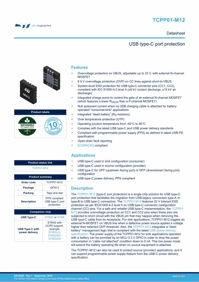
Product labels
Features• Overvoltage protection on VBUS, adjustable up to 22 V, with external N-channel
MOSFET• 6.0 V overvoltage protection (OVP) on CC lines against short-to-VBUS• System-level ESD protection for USB type-C connector pins (CC1, CC2),
compliant with IEC 61000-4-2 level 4 (±8 kV contact discharge, ±15 kV airdischarge)
• Integrated charge pump to control the gate of an external N-channel MOSFET(which features a lower RDSON than a P-channel MOSFET)
• Null quiescent current when no USB charging cable is attached for battery-operated "consumer/sink" applications
• Integrated “dead battery” (RD resistors)• Over temperature protection (OTP)• Operating junction temperature from -40°C to 85°C• Complies with the latest USB type-C and USB power delivery standards• Compliant with programmable power supply (PPS) as defined in latest USB PD
specification• Open-drain fault reporting• ECOPACK2 compliant
Applications• USB type-C used in sink configuration (consumer)• USB type-C used in source configuration (provider)• USB type-C for UFP (upstream facing port) or DFP (downstream facing port)
configuration• USB type-C power delivery, PPS compliant
DescriptionThe TCPP01-M12 (type-C port protection) is a single chip solution for USB type-Cport protection that facilitates the migration from USB legacy connectors type-A ortype-B to USB type-C connectors. The TCPP01-M12 features 22 V tolerant ESDprotection as per IEC61000-4-2 level 4 on USB type-C connector configurationchannel (CC) pins. For a safe and reliable USB type-C implementation, the TCPP01-M12 provides overvoltage protection on CC1 and CC2 pins when these pins aresubjected to short circuit with the VBUS pin that may happen when removing theUSB type-C cable from its receptacle. For sink applications, TCPP01-M12 triggers anexternal N-MOSFET on VBUS line when a defective power source applies a voltagehigher than selected OVP threshold. Also, the TCPP01-M12 integrates a “deadbattery” management logic that is compliant with the latest USB power deliveryspecification. The power supply of the TCPP01-M12 for sink applications operatedwith a battery can be provided by an MCU 3.3 V GPIO in order to drop the powerconsumption in “cable not attached” condition down to 0 nA. This low power modewill extend the battery operating life when no source equipment is attached.
The TCPP01-M12 can also be used to protect source (provider) applications, and itcan support programmable power supply feature from the USB-C power deliveryspecification.
Product status link
TCPP01-M12
Product summary
Order code TCPP01-M12
Package QFN12
Packing Tape and reel
DescriptionPPS compliant
USB type-C portprotection
Companion chip
USB Type-C STM32 or STM8
USB Type-C withpower delivery
STM32 withUCPD support,
exampleSTM32L5,STM32G0,STM32G4
USB type-C port protection
TCPP01-M12
Datasheet
DS12900 - Rev 1 - September 2019For further information contact your local STMicroelectronics sales office.
www.st.com
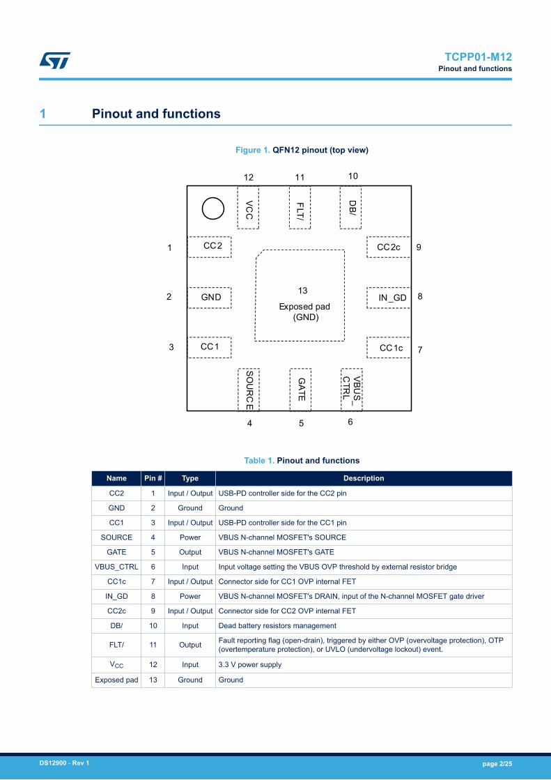
1 Pinout and functions
Figure 1. QFN12 pinout (top view)
CC2
GND
CC1
SOU
RC
E
GATE
VBUS_
CTR
L
CC1c
IN_GD
CC2c
DB/
FLT/
VCC
1
2
3
654
9
8
7
101112
13
Exposed pad (GND)
Table 1. Pinout and functions
Name Pin # Type Description
CC2 1 Input / Output USB-PD controller side for the CC2 pin
GND 2 Ground Ground
CC1 3 Input / Output USB-PD controller side for the CC1 pin
SOURCE 4 Power VBUS N-channel MOSFET's SOURCE
GATE 5 Output VBUS N-channel MOSFET's GATE
VBUS_CTRL 6 Input Input voltage setting the VBUS OVP threshold by external resistor bridge
CC1c 7 Input / Output Connector side for CC1 OVP internal FET
IN_GD 8 Power VBUS N-channel MOSFET's DRAIN, input of the N-channel MOSFET gate driver
CC2c 9 Input / Output Connector side for CC2 OVP internal FET
DB/ 10 Input Dead battery resistors management
FLT/ 11 Output Fault reporting flag (open-drain), triggered by either OVP (overvoltage protection), OTP(overtemperature protection), or UVLO (undervoltage lockout) event.
VCC 12 Input 3.3 V power supply
Exposed pad 13 Ground Ground
TCPP01-M12Pinout and functions
DS12900 - Rev 1 page 2/25
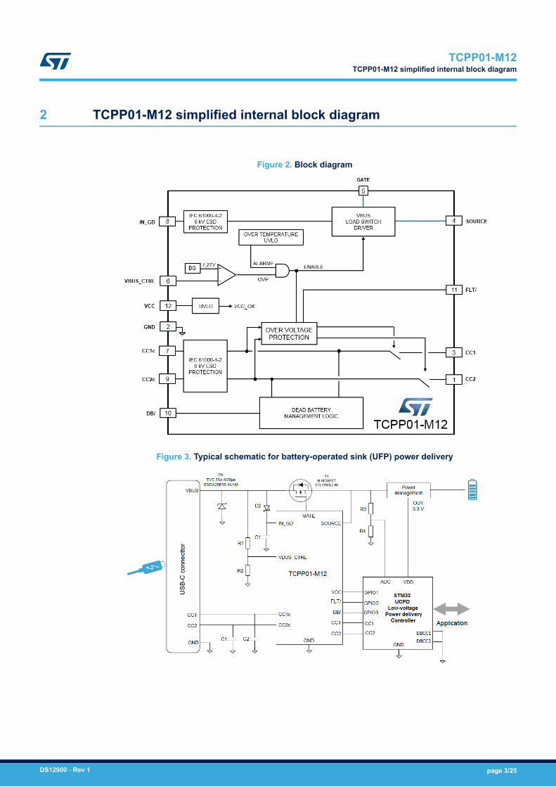
2 TCPP01-M12 simplified internal block diagram
Figure 2. Block diagram
Figure 3. Typical schematic for battery-operated sink (UFP) power delivery
TCPP01-M12TCPP01-M12 simplified internal block diagram
DS12900 - Rev 1 page 3/25
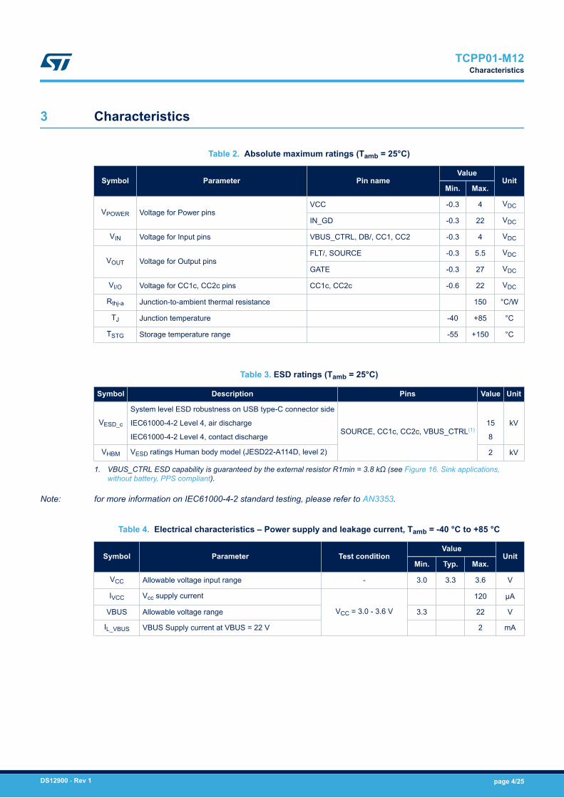
3 Characteristics
Table 2. Absolute maximum ratings (Tamb = 25°C)
Symbol Parameter Pin nameValue
UnitMin. Max.
VPOWER Voltage for Power pinsVCC -0.3 4 VDC
IN_GD -0.3 22 VDC
VIN Voltage for Input pins VBUS_CTRL, DB/, CC1, CC2 -0.3 4 VDC
VOUT Voltage for Output pinsFLT/, SOURCE -0.3 5.5 VDC
GATE -0.3 27 VDC
VI/O Voltage for CC1c, CC2c pins CC1c, CC2c -0.6 22 VDC
Rthj-a Junction-to-ambient thermal resistance 150 °C/W
TJ Junction temperature -40 +85 °C
TSTG Storage temperature range -55 +150 °C
Table 3. ESD ratings (Tamb = 25°C)
Symbol Description Pins Value Unit
VESD_c
System level ESD robustness on USB type-C connector side
IEC61000-4-2 Level 4, air discharge
IEC61000-4-2 Level 4, contact dischargeSOURCE, CC1c, CC2c, VBUS_CTRL(1)
15
8
kV
VHBM VESD ratings Human body model (JESD22-A114D, level 2) 2 kV
1. VBUS_CTRL ESD capability is guaranteed by the external resistor R1min = 3.8 kΩ (see Figure 16. Sink applications,without battery, PPS compliant).
Note: for more information on IEC61000-4-2 standard testing, please refer to AN3353.
Table 4. Electrical characteristics – Power supply and leakage current, Tamb = -40 °C to +85 °C
Symbol Parameter Test conditionValue
UnitMin. Typ. Max.
VCC Allowable voltage input range - 3.0 3.3 3.6 V
IVCC Vcc supply current
VCC = 3.0 - 3.6 V
120 µA
VBUS Allowable voltage range 3.3 22 V
IL_VBUS VBUS Supply current at VBUS = 22 V 2 mA
TCPP01-M12Characteristics
DS12900 - Rev 1 page 4/25
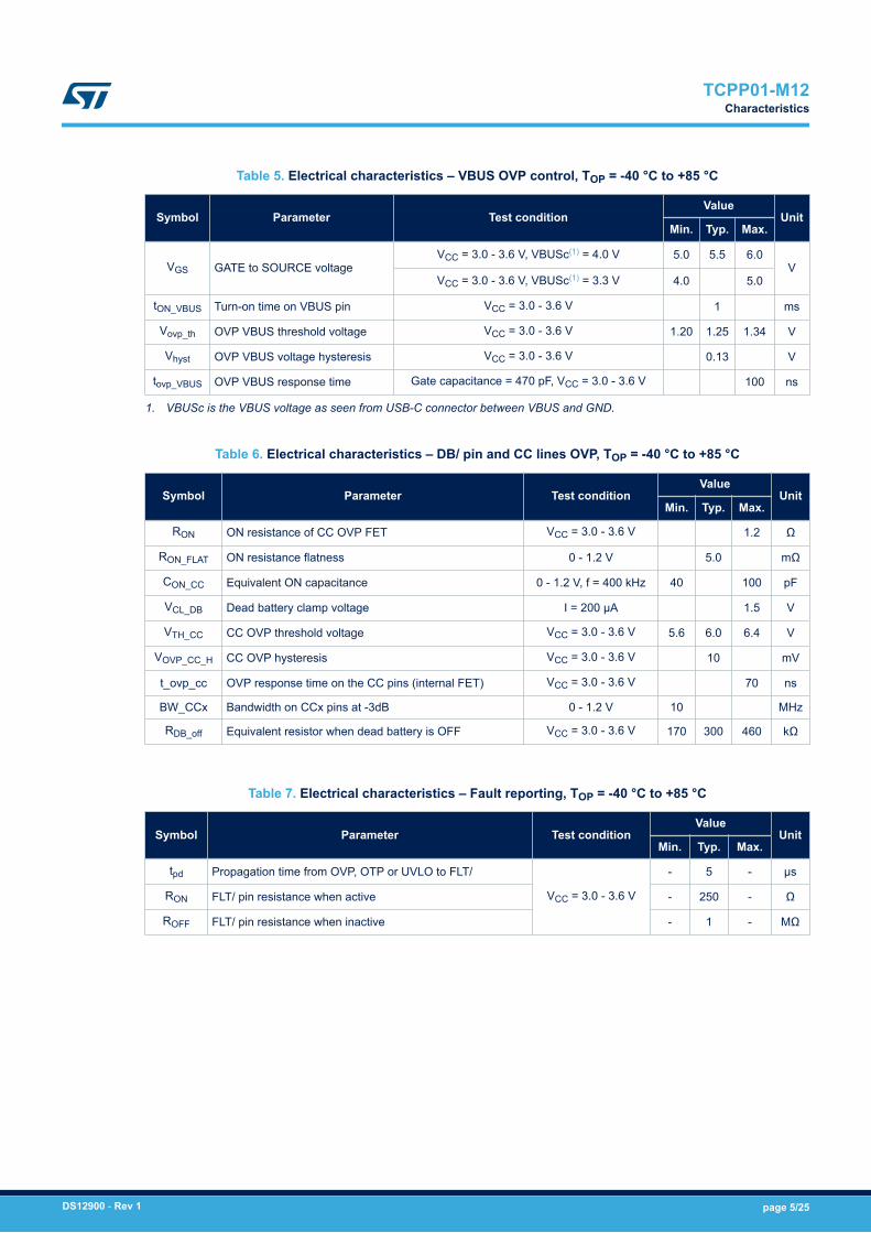
Table 5. Electrical characteristics – VBUS OVP control, TOP = -40 °C to +85 °C
Symbol Parameter Test conditionValue
UnitMin. Typ. Max.
VGS GATE to SOURCE voltageVCC = 3.0 - 3.6 V, VBUSc(1) = 4.0 V 5.0 5.5 6.0
VVCC = 3.0 - 3.6 V, VBUSc(1) = 3.3 V 4.0 5.0
tON_VBUS Turn-on time on VBUS pin VCC = 3.0 - 3.6 V 1 ms
Vovp_th OVP VBUS threshold voltage VCC = 3.0 - 3.6 V 1.20 1.25 1.34 V
Vhyst OVP VBUS voltage hysteresis VCC = 3.0 - 3.6 V 0.13 V
tovp_VBUS OVP VBUS response time Gate capacitance = 470 pF, VCC = 3.0 - 3.6 V 100 ns
1. VBUSc is the VBUS voltage as seen from USB-C connector between VBUS and GND.
Table 6. Electrical characteristics – DB/ pin and CC lines OVP, TOP = -40 °C to +85 °C
Symbol Parameter Test conditionValue
UnitMin. Typ. Max.
RON ON resistance of CC OVP FET VCC = 3.0 - 3.6 V 1.2 Ω
RON_FLAT ON resistance flatness 0 - 1.2 V 5.0 mΩ
CON_CC Equivalent ON capacitance 0 - 1.2 V, f = 400 kHz 40 100 pF
VCL_DB Dead battery clamp voltage I = 200 µA 1.5 V
VTH_CC CC OVP threshold voltage VCC = 3.0 - 3.6 V 5.6 6.0 6.4 V
VOVP_CC_H CC OVP hysteresis VCC = 3.0 - 3.6 V 10 mV
t_ovp_cc OVP response time on the CC pins (internal FET) VCC = 3.0 - 3.6 V 70 ns
BW_CCx Bandwidth on CCx pins at -3dB 0 - 1.2 V 10 MHz
RDB_off Equivalent resistor when dead battery is OFF VCC = 3.0 - 3.6 V 170 300 460 kΩ
Table 7. Electrical characteristics – Fault reporting, TOP = -40 °C to +85 °C
Symbol Parameter Test conditionValue
UnitMin. Typ. Max.
tpd Propagation time from OVP, OTP or UVLO to FLT/
VCC = 3.0 - 3.6 V
- 5 - µs
RON FLT/ pin resistance when active - 250 - Ω
ROFF FLT/ pin resistance when inactive - 1 - MΩ
TCPP01-M12Characteristics
DS12900 - Rev 1 page 5/25
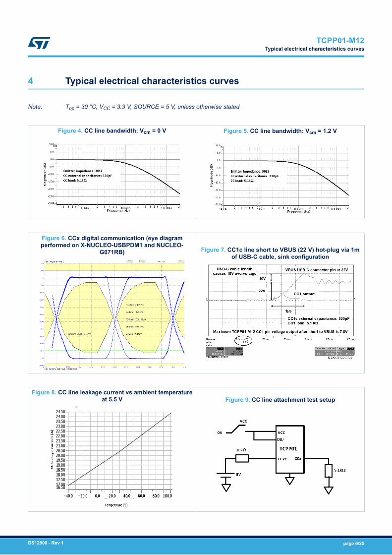
4 Typical electrical characteristics curves
Note: Top = 30 °C, VCC = 3.3 V, SOURCE = 5 V, unless otherwise stated
Figure 4. CC line bandwidth: Vcm = 0 V Figure 5. CC line bandwidth: Vcm = 1.2 V
Figure 6. CCx digital communication (eye diagramperformed on X-NUCLEO-USBPDM1 and NUCLEO-
G071RB) Figure 7. CC1c line short to VBUS (22 V) hot-plug via 1mof USB-C cable, sink configuration
Figure 8. CC line leakage current vs ambient temperatureat 5.5 V Figure 9. CC line attachment test setup
TCPP01-M12Typical electrical characteristics curves
DS12900 - Rev 1 page 6/25
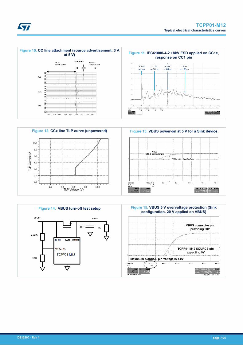
Figure 10. CC line attachment (source advertisement: 3 Aat 5 V) Figure 11. IEC61000-4-2 +8kV ESD applied on CC1c,
response on CC1 pin
Figure 12. CCx line TLP curve (unpowered) Figure 13. VBUS power-on at 5 V for a Sink device
Figure 14. VBUS turn-off test setup Figure 15. VBUS 5 V overvoltage protection (Sinkconfiguration, 20 V applied on VBUS)
TCPP01-M12Typical electrical characteristics curves
DS12900 - Rev 1 page 7/25
5 Application
5.1 General information
The sections below are not part of the ST product specification. They are intended to give a generic applicationoverview to be used by the customer as a starting point for further implementations and customizations.ST does not warrant compliance with customer specifications. Full system implementation and validation areunder the customer’s responsibility.
5.2 Electrical hazards related to USB Type-C
Applications using an USB Type-C connector must be protected against three kinds of hazards:
5.2.1 CC lines short to VBUSThis happens when VBUS high voltage short circuit to the CC lines when hot unplug is done with a poormechanical quality connector. Over voltage protection is needed on the CC lines because VBUS typical voltagecan be as high as 20 V when CC pins are usually 5 V tolerant I/Os on low voltage USB-PHY controllers.
5.2.2 Defective chargerVBUS line is compromised if a defective charger is stuck at a high voltage.Overvoltage protection is always required on the VBUS line to prevent a voltage higher than negociated is appliedon the VBUS.This use case can occur even when power delivery is not used i.e when VBUS voltage is 5 V
5.2.3 Electrostatic discharge (ESD)Electrostatic discharges can be conducted by the USB Type-C connector and damage the electronic circuitry ofthe application.The ESD surge waveform is modelized by the international electrotechnical commission in the specificationIEC61000-4-2.For more information on IEC61000-4-2 standard testing, please refer to STMicroelectronics application noteAN3353.
5.3 USB Type-C protection
Any application using an USB Type-C connector must use a Type-C port protection against above listed electricalhazards.STMicroelectronics TCPP01-M12 (Type-C port protection housed in QFN12) is a single-chip cost effectivesolution to protect any application using a USB Type-C connector.It is especially adapted to SINK (consumer) or SOURCE (provider) applications.The TCPP01-M12 provides 20 V short-to-VBUS over-voltage and system-level ESD protection on CC lines, aswell as adjustable over-voltage protection for the VBUS line: an external N-channel MOSFET gate driver isintegrated inside TCPP01-M12.Also, TCPP01-M12 integrates dead battery management logic.For consumer (sink) configurations, TCPP01-M12 features a null quiescent current thanks to TCPP01-M12 VCCpin being directly controlled by a MCU GPIO in this configuration.TCPP01-M12 is the companion chip for:• any general purpose MCUs (example: STM32, STM8) used for USB-C charging applications exposed to
defective charger and electrostatic discharge.• any low voltage USB power delivery controller (for example: STM32-UCPD like STM32G0 and STM32G4),
exposed to short to VBUS, defective charger and electrostatic discharge.
TCPP01-M12Application
DS12900 - Rev 1 page 8/25
5.4 USB charging system scalability
Thanks to its simple implementation and system compliancy with both legacy USB charging and latest USBpower delivery specification, USB-C applications using TCPP01-M12 can simply migrate from legacy USBcharging (see Figure 19) to USB power delivery charging (see Figure 20) by simply swapping their STM32 fromgeneral purpose (for example: STM32L0) to general purpose + UCPD (example: STM23G0) and remove C1/C2and add R5/R6 in the PCB to take benefit of the USB-C power delivery. Empty PCB footprints can be plannedearlier in the design to allow this system scalability.
5.5 How to handle dead battery (DB) condition with the TCPP01-M12
Dead battery use case happens when a battery-operated sink (consumer or UFP) application has its battery fullydepleted. In this case TCPP01-M12 enters into dead battery operation.Dead battery behavior is basically a pull down (Rd) or a voltage clamp when a USB type-C source voltage isapplied to CC. It is interpreted as a request by the sink to receive VBUS. It thus facilitates the charging ofequipment with a fully depleted battery:• It must be present in most cases• It must not be present in the case of a (pure) type-C Source, for example a wall charger
The DB/ or 'dead battery resistor management' pin is a pulled-down active-low TCPP01-M12 input. The DB/ pincan be used in two ways:• The DB/ pin is connected to VCC or• The DB/ pin is driven by an MCU GPIO
As long as the DB/ pin is low or high-impedance (an internal 5 kΩ pull-down sets the level to ‘0’), the dead-batteryresistors are connected and CC switches are open (OFF state).When the DB/ pin is tied to VCC, the DB/ resistors are disconnected and CC OVP switches are closed (ON state).DB/ usage in SINK (SNK) applications:• After system power-up, the DB/ pin must be kept at 0. In this case Rd is enabled at TCPP01-M12 level.• Once Rd is enabled in the UCPD (USB-C power delivery controller), the DB/ pin must be set to the logic
level '1'
For DB/ usage in SRC or Source mode, the DB/ pin must be tied to VCC.
Table 8. Dead battery logic states
TCPP01-M12
VCC
TCPP01-M12
DB/
TCPP01-M12
DB clamp present
TCPP01-M12
CC1/CC2 OVP FETstate
TCPP01-M12
DB function state
0 0 Yes Open Activated
0 1 Yes Open Activated
1 0 Yes Open Activated
1 1 No Closed Inactivated
Note: When STM32-UCPD boots, Rd seen on CC lines are coming from TCPP01-M12. When STM32-UCPD haswake-up, Rd from TCPP01-M12 are disconnected and STM32-UCPD set Rd on CC lines from UCPD IP
TCPP01-M12USB charging system scalability
DS12900 - Rev 1 page 9/25
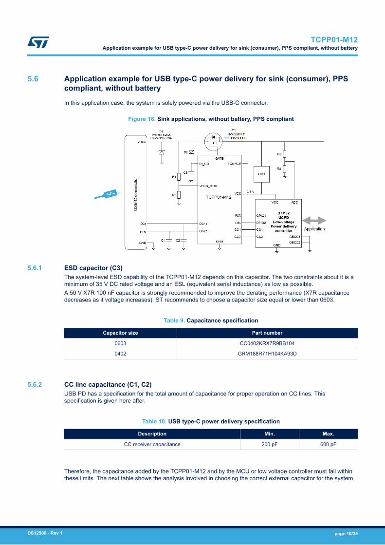
5.6 Application example for USB type-C power delivery for sink (consumer), PPScompliant, without battery
In this application case, the system is solely powered via the USB-C connector.
Figure 16. Sink applications, without battery, PPS compliant
5.6.1 ESD capacitor (C3)The system-level ESD capability of the TCPP01-M12 depends on this capacitor. The two constraints about it is aminimum of 35 V DC rated voltage and an ESL (equivalent serial inductance) as low as possible.A 50 V X7R 100 nF capacitor is strongly recommended to improve the derating performance (X7R capacitancedecreases as it voltage increases). ST recommends to choose a capacitor size equal or lower than 0603.
Table 9. Capacitance specification
Capacitor size Part number
0603 CC0402KRX7R9BB104
0402 GRM188R71H104KA93D
5.6.2 CC line capacitance (C1, C2)USB PD has a specification for the total amount of capacitance for proper operation on CC lines. Thisspecification is given here after.
Table 10. USB type-C power delivery specification
Description Min. Max.
CC receiver capacitance 200 pF 600 pF
Therefore, the capacitance added by the TCPP01-M12 and by the MCU or low voltage controller must fall withinthese limits. The next table shows the analysis involved in choosing the correct external capacitor for the system.
TCPP01-M12Application example for USB type-C power delivery for sink (consumer), PPS compliant, without battery
DS12900 - Rev 1 page 10/25
Table 11. CC line capacitance budget analysis
CC capacitance Min. Max. Comment
CC line target capacitor 200 pF 600 pF From USB PD Specification Section 5.8.6
TCPP01-M12 CC1c, CC2c capacitance 40 pF 100 pF
MCU capacitance 60 pF 90 pF Typical value. To be adapted following the exact reference used
Proposed capacitance C1, C2 120 pF 390 pF 25 V DC min. of rated voltage 0402 or smaller recommended
5.6.3 Sense resistor (R1, R2)VBUS OVP triggers when VBUS_CTRL pin rises above 1.25 V typical. Choose R1 from any value between 5 kΩand 10 kΩ and calculate R2 as follows:
With:• R1 = arbitrary resistor between 5-10 kΩ• VBUScMAX = desired VBUS OVP threshold level• VBUS_CTRL = 1.25 V (typical)
5.6.4 N-channel MOSFET (T1)The TCPP01-M12 ensures a VGS voltage between 5 V and 6 V when the N-channel MOSFET is ON: choose a N-channel MOSFET fully specified (for example: STL11N3LLH6) with 5 V of VGS. Maximum current in USB-PDapplications can raises up to 5 A.
5.6.5 Complementary products for USB dataline protection for pins DP, DM, SSRX, SSTXFor applications requiring USB dataline protection, STMicroelectronics recommends the implementation shown inpicture below:
TCPP01-M12Application example for USB type-C power delivery for sink (consumer), PPS compliant, without battery
DS12900 - Rev 1 page 11/25
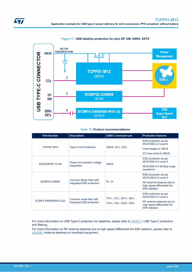
Figure 17. USB dataline protection for pins DP, DM, SSRX, SSTX
Table 12. Product recommendations
Part Number Description USB-C connector pin Protection features
TCPP01-M12 Type-C Port Protection VBUS, CC1, CC2
ESD protection as perIEC61000-4-2 Level 4
Overvoltage on VBUS
CC lines short to VBUS
ESDA25P35-1U1M Power line transient voltagesuppressor VBUS
ESD protection as perIEC61000-4-2 Level 4
IEC61000-4-5 (8/20µs surgewaveform)
ECMF02-2AMX6 Common Mode Filter withintegrated ESD protection D+, D-
ESD protection as perIEC61000-4-2 Level 4
RF antenna desense due tohigh speed differential linkEMI radiation
ECMF4-2450A60N10 (x2) Common mode filter withintegrated ESD protection
TX1+, TX1-, RX1+, RX1-
TX2+, TX2-, RX2+, RX2-
ESD protection as perIEC61000-4-2 Level 4
RF antenna desense due tohigh speed differential linkEMI radiation
For more information on USB Type-C protection for datalines, please refer to AN4871, USB Type-C protectionand filtering.For more information on RF antenna desense due to high speed differential link EMI radiation, please refer toAN4356, Antenna desense on handheld equipment.
TCPP01-M12Application example for USB type-C power delivery for sink (consumer), PPS compliant, without battery
DS12900 - Rev 1 page 12/25
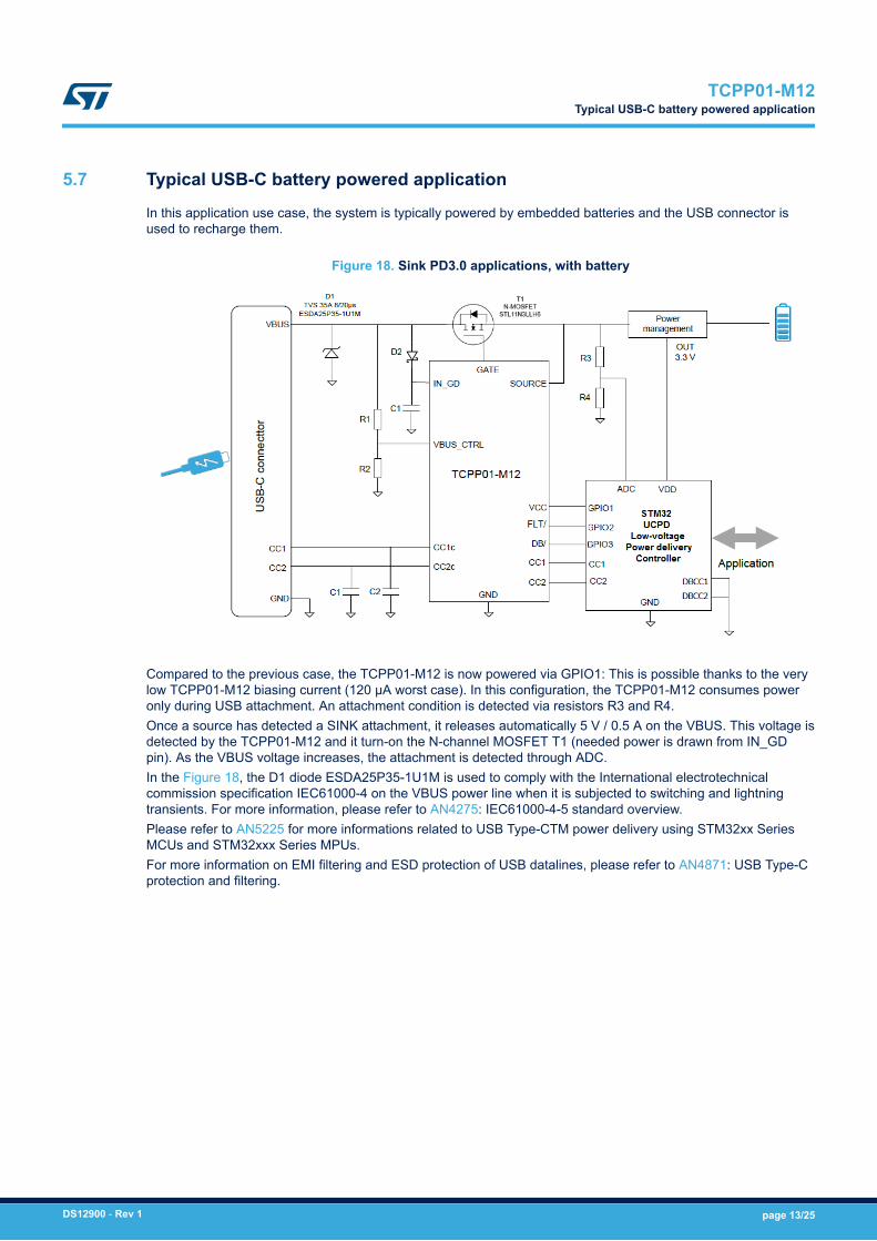
5.7 Typical USB-C battery powered application
In this application use case, the system is typically powered by embedded batteries and the USB connector isused to recharge them.
Figure 18. Sink PD3.0 applications, with battery
Compared to the previous case, the TCPP01-M12 is now powered via GPIO1: This is possible thanks to the verylow TCPP01-M12 biasing current (120 µA worst case). In this configuration, the TCPP01-M12 consumes poweronly during USB attachment. An attachment condition is detected via resistors R3 and R4.Once a source has detected a SINK attachment, it releases automatically 5 V / 0.5 A on the VBUS. This voltage isdetected by the TCPP01-M12 and it turn-on the N-channel MOSFET T1 (needed power is drawn from IN_GDpin). As the VBUS voltage increases, the attachment is detected through ADC.In the Figure 18, the D1 diode ESDA25P35-1U1M is used to comply with the International electrotechnicalcommission specification IEC61000-4 on the VBUS power line when it is subjected to switching and lightningtransients. For more information, please refer to AN4275: IEC61000-4-5 standard overview.Please refer to AN5225 for more informations related to USB Type-CTM power delivery using STM32xx SeriesMCUs and STM32xxx Series MPUs.For more information on EMI filtering and ESD protection of USB datalines, please refer to AN4871: USB Type-Cprotection and filtering.
TCPP01-M12Typical USB-C battery powered application
DS12900 - Rev 1 page 13/25
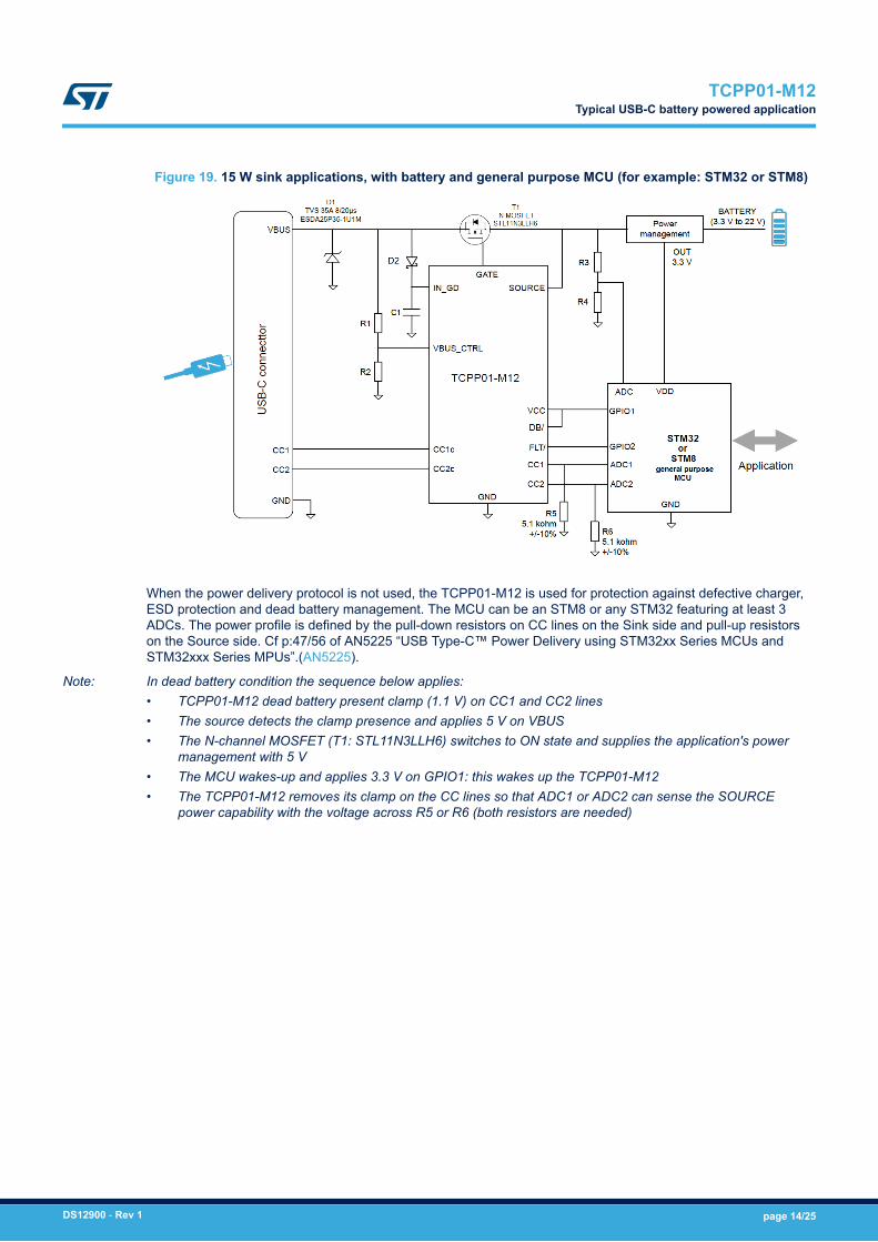
Figure 19. 15 W sink applications, with battery and general purpose MCU (for example: STM32 or STM8)
When the power delivery protocol is not used, the TCPP01-M12 is used for protection against defective charger,ESD protection and dead battery management. The MCU can be an STM8 or any STM32 featuring at least 3ADCs. The power profile is defined by the pull-down resistors on CC lines on the Sink side and pull-up resistorson the Source side. Cf p:47/56 of AN5225 “USB Type-C™ Power Delivery using STM32xx Series MCUs andSTM32xxx Series MPUs”.(AN5225).
Note: In dead battery condition the sequence below applies:• TCPP01-M12 dead battery present clamp (1.1 V) on CC1 and CC2 lines• The source detects the clamp presence and applies 5 V on VBUS• The N-channel MOSFET (T1: STL11N3LLH6) switches to ON state and supplies the application's power
management with 5 V• The MCU wakes-up and applies 3.3 V on GPIO1: this wakes up the TCPP01-M12• The TCPP01-M12 removes its clamp on the CC lines so that ADC1 or ADC2 can sense the SOURCE
power capability with the voltage across R5 or R6 (both resistors are needed)
TCPP01-M12Typical USB-C battery powered application
DS12900 - Rev 1 page 14/25
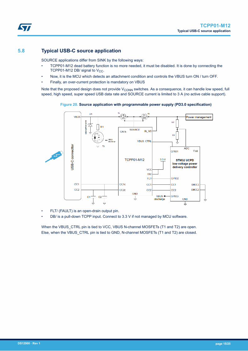
5.8 Typical USB-C source application
SOURCE applications differ from SINK by the following ways:• TCPP01-M12 dead battery function is no more needed, it must be disabled. It is done by connecting the
TCPP01-M12 DB/ signal to VCC.• Now, it is the MCU which detects an attachment condition and controls the VBUS turn ON / turn OFF.• Finally, an over-current protection is mandatory on VBUS
Note that the proposed design does not provide VCONN switches. As a consequence, it can handle low speed, fullspeed, high speed, super speed USB data rate and SOURCE current is limited to 3 A (no active cable support).
Figure 20. Source application with programmable power supply (PD3.0 specification)
• FLT/ (FAULT) is an open-drain output pin.• DB/ is a pull-down TCPP input. Connect to 3.3 V if not managed by MCU software.
When the VBUS_CTRL pin is tied to VCC, VBUS N-channel MOSFETs (T1 and T2) are open.Else, when the VBUS_CTRL pin is tied to GND, N-channel MOSFETs (T1 and T2) are closed.
TCPP01-M12Typical USB-C source application
DS12900 - Rev 1 page 15/25
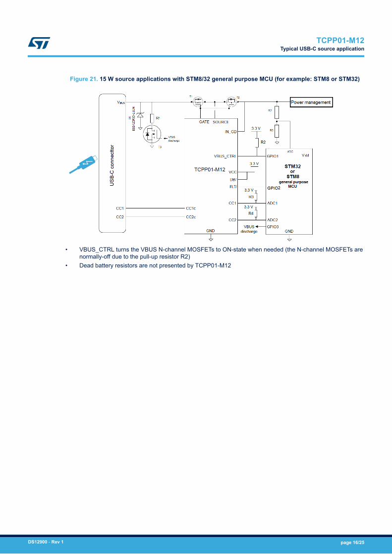
Figure 21. 15 W source applications with STM8/32 general purpose MCU (for example: STM8 or STM32)
• VBUS_CTRL turns the VBUS N-channel MOSFETs to ON-state when needed (the N-channel MOSFETs arenormally-off due to the pull-up resistor R2)
• Dead battery resistors are not presented by TCPP01-M12
TCPP01-M12Typical USB-C source application
DS12900 - Rev 1 page 16/25
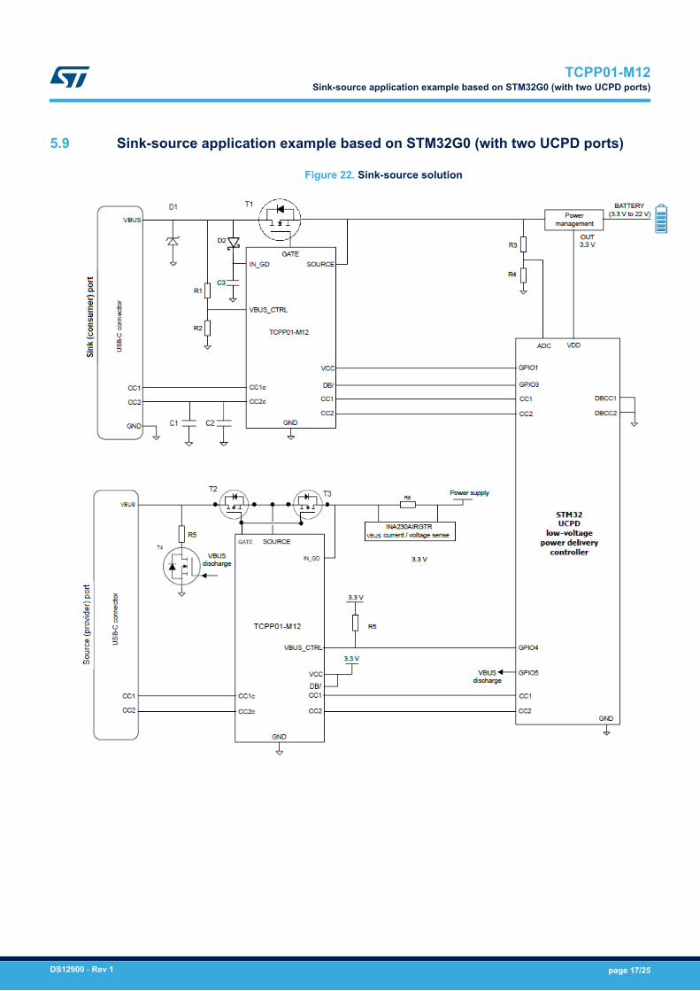
5.9 Sink-source application example based on STM32G0 (with two UCPD ports)
Figure 22. Sink-source solution
TCPP01-M12Sink-source application example based on STM32G0 (with two UCPD ports)
DS12900 - Rev 1 page 17/25
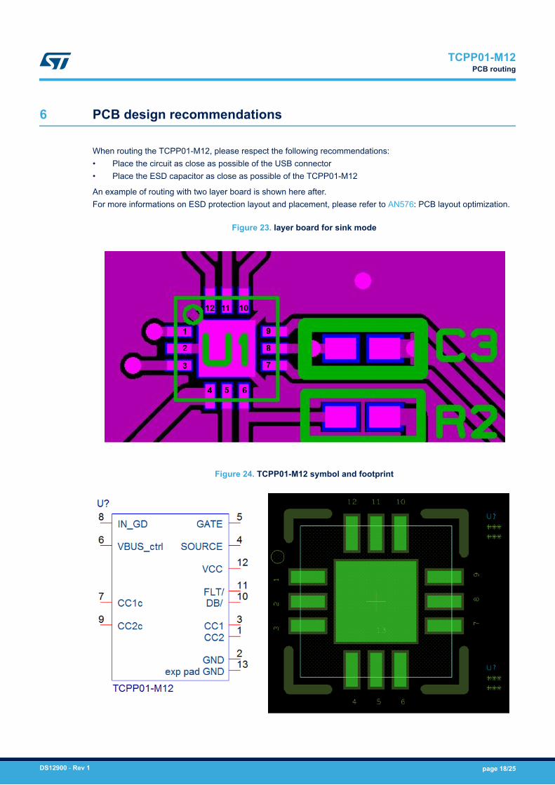
6 PCB design recommendations
When routing the TCPP01-M12, please respect the following recommendations:• Place the circuit as close as possible of the USB connector• Place the ESD capacitor as close as possible of the TCPP01-M12
An example of routing with two layer board is shown here after.For more informations on ESD protection layout and placement, please refer to AN576: PCB layout optimization.
Figure 23. layer board for sink mode
Figure 24. TCPP01-M12 symbol and footprint
TCPP01-M12PCB routing
DS12900 - Rev 1 page 18/25
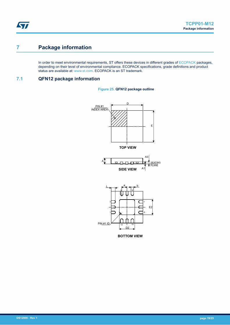
7 Package information
In order to meet environmental requirements, ST offers these devices in different grades of ECOPACK packages,depending on their level of environmental compliance. ECOPACK specifications, grade definitions and productstatus are available at: www.st.com. ECOPACK is an ST trademark.
7.1 QFN12 package information
Figure 25. QFN12 package outline
E2
e bL
PIN #1 ID
6
7
9
1012
1
3
4
D2
SIDE VIEW
BOTTOM VIEW
A1
A3A SEATING
PLANE
TOP VIEW
E
DPIN #1
INDEX AREA
TCPP01-M12Package information
DS12900 - Rev 1 page 19/25
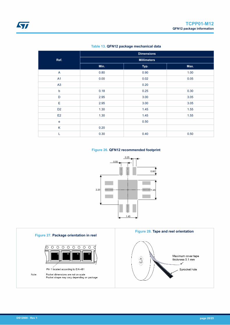
Table 13. QFN12 package mechanical data
Ref.
Dimensions
Millimeters
Min. Typ. Max.
A 0.80 0.90 1.00
A1 0.00 0.02 0.05
A3 0.20
b 0.18 0.25 0.30
D 2.95 3.00 3.05
E 2.95 3.00 3.05
D2 1.30 1.45 1.55
E2 1.30 1.45 1.55
e 0.50
K 0.20
L 0.30 0.40 0.50
Figure 26. QFN12 recommended footprint
0.25
0.50
0.60
1.45
1.45
2.20
Figure 27. Package orientation in reelFigure 28. Tape and reel orientation
TCPP01-M12QFN12 package information
DS12900 - Rev 1 page 20/25
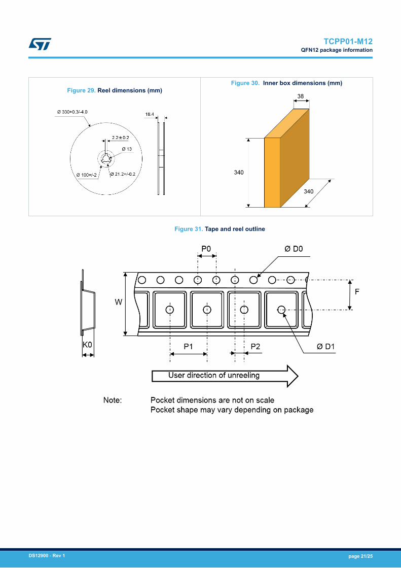
Figure 29. Reel dimensions (mm)Figure 30. Inner box dimensions (mm)
Figure 31. Tape and reel outline
TCPP01-M12QFN12 package information
DS12900 - Rev 1 page 21/25
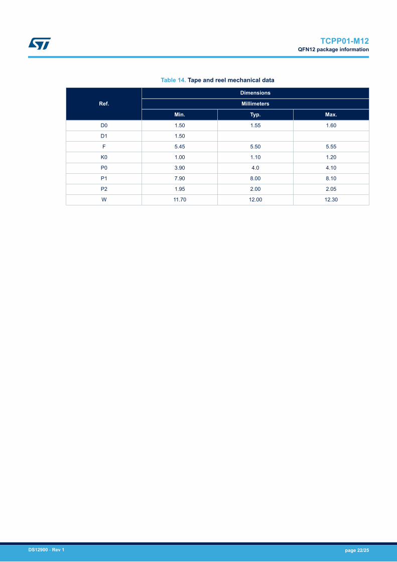
Table 14. Tape and reel mechanical data
Ref.
Dimensions
Millimeters
Min. Typ. Max.
D0 1.50 1.55 1.60
D1 1.50
F 5.45 5.50 5.55
K0 1.00 1.10 1.20
P0 3.90 4.0 4.10
P1 7.90 8.00 8.10
P2 1.95 2.00 2.05
W 11.70 12.00 12.30
TCPP01-M12QFN12 package information
DS12900 - Rev 1 page 22/25
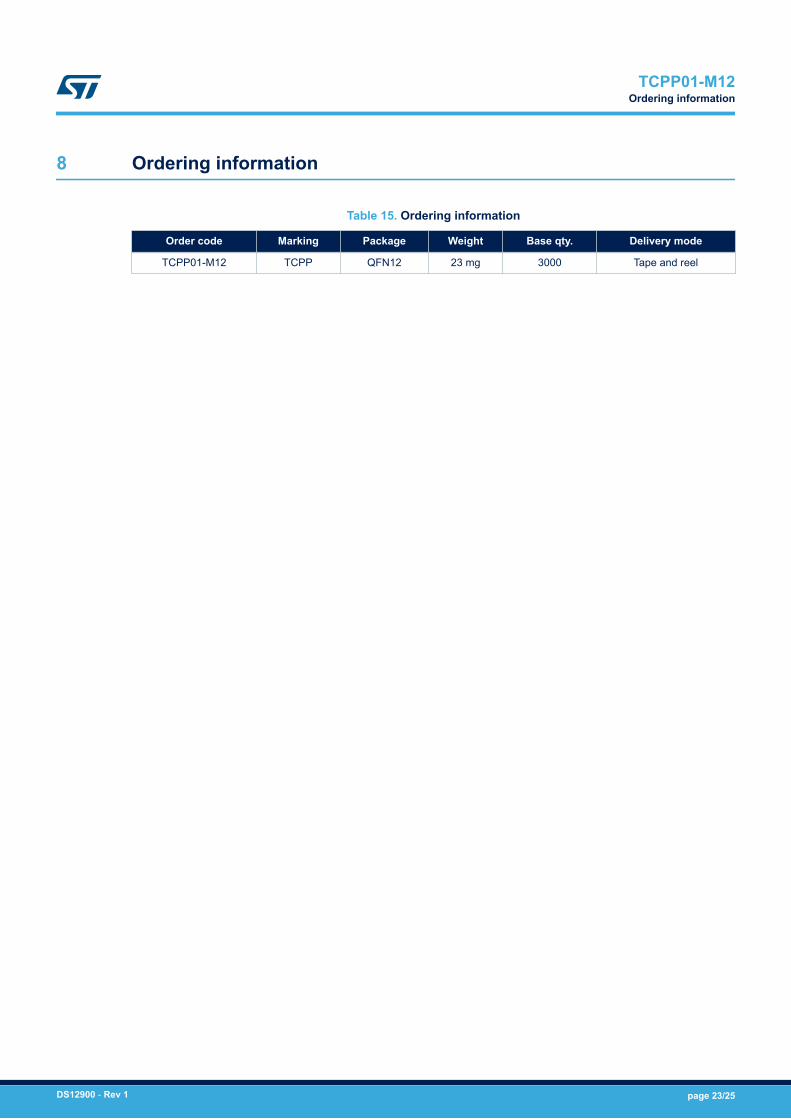
8 Ordering information
Table 15. Ordering information
Order code Marking Package Weight Base qty. Delivery mode
TCPP01-M12 TCPP QFN12 23 mg 3000 Tape and reel
TCPP01-M12Ordering information
DS12900 - Rev 1 page 23/25
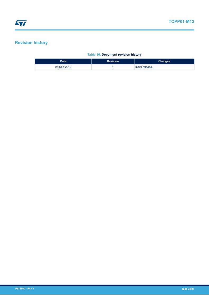
Revision history
Table 16. Document revision history
Date Revision Changes
06-Sep-2019 1 Initial release.
TCPP01-M12
DS12900 - Rev 1 page 24/25
IMPORTANT NOTICE – PLEASE READ CAREFULLY
STMicroelectronics NV and its subsidiaries (“ST”) reserve the right to make changes, corrections, enhancements, modifications, and improvements to STproducts and/or to this document at any time without notice. Purchasers should obtain the latest relevant information on ST products before placing orders. STproducts are sold pursuant to ST’s terms and conditions of sale in place at the time of order acknowledgement.
Purchasers are solely responsible for the choice, selection, and use of ST products and ST assumes no liability for application assistance or the design ofPurchasers’ products.
No license, express or implied, to any intellectual property right is granted by ST herein.
Resale of ST products with provisions different from the information set forth herein shall void any warranty granted by ST for such product.
ST and the ST logo are trademarks of ST. For additional information about ST trademarks, please refer to www.st.com/trademarks. All other product or servicenames are the property of their respective owners.
Information in this document supersedes and replaces information previously supplied in any prior versions of this document.
© 2019 STMicroelectronics – All rights reserved
TCPP01-M12
DS12900 - Rev 1 page 25/25