special vehicle for transporting unstable chemicals
TRANSCRIPT

Special Vehicle for Transporting
Unstable Chemicals
By
Gong, Zhangxiaowen
Ma, Jun
Zhou, Wenjia
Final Report for ECE 445, Senior Design, Spring 2012
TA: Fortier, Justine
1 May 2012
Project No. 15

Abstract
This project is to design a special vehicle for transporting volatile substances. The purpose is to minimize the
vibration and inclination of the vehicle when moving on an uneven surface.
The design actualizes the following functions: an omni-directional movement system that not only eliminates the
centrifugal force when the vehicle turns but also makes the vehicle agile in compact lab environment, an auto leveling
system that allows the vehicle to adapt uneven surface thus reduces vibration, and a real time wireless communication
channel between the vehicle and an upper computer that provides features such as remote control and sensor data
recording for further analysis.
Most functionalities described above have been fulfilled as intended. However, a torque issue impedes the performance
of the auto leveling. As a result, a re-design for the mechanical system is scheduled in the future.
i

Contents
1 Introduction . . . . . . . . . . . . . . . . . . . . . . . . . . . . . . . . . . . . . . . . . . . . . . . . . . . . . . . . . . . . . . . 1
1.1 Purpose and Goal . . . . . . . . . . . . . . . . . . . . . . . . . . . . . . . . . . . . . . . . . . . . . . . . . . . . . . . . . 1
1.2 Functions . . . . . . . . . . . . . . . . . . . . . . . . . . . . . . . . . . . . . . . . . . . . . . . . . . . . . . . . . . . . . . . 1
1.3 Design Block . . . . . . . . . . . . . . . . . . . . . . . . . . . . . . . . . . . . . . . . . . . . . . . . . . . . . . . . . . . . 1
2 Design. . . . . . . . . . . . . . . . . . . . . . . . . . . . . . . . . . . . . . . . . . . . . . . . . . . . . . . . . . . . . . . . . . . . 3
2.1 Design Procedure . . . . . . . . . . . . . . . . . . . . . . . . . . . . . . . . . . . . . . . . . . . . . . . . . . . . . . . . . 3
2.1.1 Mechanical System. . . . . . . . . . . . . . . . . . . . . . . . . . . . . . . . . . . . . . . . . . . . . . . . . . . . . 3
2.1.2 Electrical/Electronic System. . . . . . . . . . . . . . . . . . . . . . . . . . . . . . . . . . . . . . . . . . . . . . 3
2.2 Design Details. . . . . . . . . . . . . . . . . . . . . . . . . . . . . . . . . . . . . . . . . . . . . . . . . . . . . . . . . . . . 5
2.2.1 Schematics. . . . . . . . . . . . . . . . . . . . . . . . . . . . . . . . . . . . . . . . . . . . . . . . . . . . . . . . . . . 5
2.2.2 Software . . . . . . . . . . . . . . . . . . . . . . . . . . . . . . . . . . . . . . . . . . . . . . . . . . . . . . . . . . . . 9
3 Design Verification . . . . . . . . . . . . . . . . . . . . . . . . . . . . . . . . . . . . . . . . . . . . . . . . . . . . . . . . . . . 16
3.1 Master Controller . . . . . . . . . . . . . . . . . . . . . . . . . . . . . . . . . . . . . . . . . . . . . . . . . . . . . . . . . 16
3.2 MEMS Sensors . . . . . . . . . . . . . . . . . . . . . . . . . . . . . . . . . . . . . . . . . . . . . . . . . . . . . . . . . . . 16
3.3 ODM System . . . . . . . . . . . . . . . . . . . . . . . . . . . . . . . . . . . . . . . . . . . . . . . . . . . . . . . . . . . . 17
3.4 AL System . . . . . . . . . . . . . . . . . . . . . . . . . . . . . . . . . . . . . . . . . . . . . . . . . . . . . . . . . . . . . . 17
4 Cost . . . . . . . . . . . . . . . . . . . . . . . . . . . . . . . . . . . . . . . . . . . . . . . . . . . . . . . . . . . . . . . . . . . . . 18
4.1 Parts . . . . . . . . . . . . . . . . . . . . . . . . . . . . . . . . . . . . . . . . . . . . . . . . . . . . . . . . . . . . . . . . . . 18
4.2 Labor . . . . . . . . . . . . . . . . . . . . . . . . . . . . . . . . . . . . . . . . . . . . . . . . . . . . . . . . . . . . . . . . . . 18
5 Conclusion. . . . . . . . . . . . . . . . . . . . . . . . . . . . . . . . . . . . . . . . . . . . . . . . . . . . . . . . . . . . . . . . . 19
5.1 Accomplishments and Future Work . . . . . . . . . . . . . . . . . . . . . . . . . . . . . . . . . . . . . . . . . . . . 19
5.2 Uncertainties . . . . . . . . . . . . . . . . . . . . . . . . . . . . . . . . . . . . . . . . . . . . . . . . . . . . . . . . . . . . 19
5.3 Ethical considerations . . . . . . . . . . . . . . . . . . . . . . . . . . . . . . . . . . . . . . . . . . . . . . . . . . . . . . 19
Reference . . . . . . . . . . . . . . . . . . . . . . . . . . . . . . . . . . . . . . . . . . . . . . . . . . . . . . . . . . . . . . . . . . . . 20
Appendix A Requirement and Verification Table . . . . . . . . . . . . . . . . . . . . . . . . . . . . . . . . . . . . . . 21
A.1 Main Controller . . . . . . . . . . . . . . . . . . . . . . . . . . . . . . . . . . . . . . . . . . . . . . . . . . . . . . . . . . 21
A.2 MEMS Sensors . . . . . . . . . . . . . . . . . . . . . . . . . . . . . . . . . . . . . . . . . . . . . . . . . . . . . . . . . . . 24
A.3 Side Controllers . . . . . . . . . . . . . . . . . . . . . . . . . . . . . . . . . . . . . . . . . . . . . . . . . . . . . . . . . . 25
A.4 Wireless Communication . . . . . . . . . . . . . . . . . . . . . . . . . . . . . . . . . . . . . . . . . . . . . . . . . . . . 27
A.5 Omni-directional Movement. . . . . . . . . . . . . . . . . . . . . . . . . . . . . . . . . . . . . . . . . . . . . . . . . . 28
A.6 Active Suspension . . . . . . . . . . . . . . . . . . . . . . . . . . . . . . . . . . . . . . . . . . . . . . . . . . . . . . . . . 30
ii

A.7 PC Receiver . . . . . . . . . . . . . . . . . . . . . . . . . . . . . . . . . . . . . . . . . . . . . . . . . . . . . . . . . . . . . 31
A.8 Power Management . . . . . . . . . . . . . . . . . . . . . . . . . . . . . . . . . . . . . . . . . . . . . . . . . . . . . . . . 32
Appendix B Full Schematics and PCB Layouts. . . . . . . . . . . . . . . . . . . . . . . . . . . . . . . . . . . . . . . . 34
B.1 The Master Controller. . . . . . . . . . . . . . . . . . . . . . . . . . . . . . . . . . . . . . . . . . . . . . . . . . . . . . 34
B.2 The Slave Controllers . . . . . . . . . . . . . . . . . . . . . . . . . . . . . . . . . . . . . . . . . . . . . . . . . . . . . . 35
B.3 The PC Receiver. . . . . . . . . . . . . . . . . . . . . . . . . . . . . . . . . . . . . . . . . . . . . . . . . . . . . . . . . . 36
iii

1 Introduction
1.1 Purpose and Goal
Our project is to design a special vehicle for transporting chemicals. The motivation came to us during a
chemistry lab session. We noticed that when using a normal cart to carry chemicals, the carrier experienced
significant bumps. Since volatile and hazardous chemicals should be treated carefully, we decided to address
the issue by building a robot that performs safe and efficient transportation for those unstable chemicals.
The major goal for the design is to keep the chassis level and stable; therefore, the vehicle has to limit the
vibration and the tilt of the chassis while traveling on different road conditions.
1.2 Functions
The system has 4 major functions:
1. Motion analysis: The on-board processor acquires data from MEMS (MicroElectroMechanical Sys-
tems) sensors and calculates real-time tilt angle according to the readings. In order to eliminate noises,
the raw data from the sensors have to be filtered.
2. AL (Auto Leveling) system: A worm motor based auto leveling system allows the vehicle to adapt
uneven surface thus reduces vibration. In order to effectively reduce vibration, the suspension has to
respond to uneven surfaces within 0.3s. The maximum dynamic tilt angle between the chassis and the
horizontal surface also has to be constrained in 5 degree.
3. ODM (Omni-Directional Movement) system: A system built by servos and PID controlled
motors not only eliminates the centrifugal force when the vehicle turns but also makes the vehicle agile
in compact lab environment. All 4 wheels in the system should be adjusted to the same direction,
rotate at the same speed, and modify their speed respectively when encountering uneven surface.
4. Real time wireless communication A wireless link between the vehicle and an upper computer
provides features such as remote control and sensor data recording for further analysis.
1.3 Design Block
The project consists of seven modules. Figure 1 is the main block diagram of the system.
1

Active lev-
eling and
omni-direction
movement
system
Slave con-
trollers
Master
controller
Power man-
agement
MEMS sensors
Wireless
interfacePC receiver
PWM
Position
feedback
SPI
USB
I2C
I2C
Electrical
Vehicle
Mechanical
Figure 1: Main block diagram
1. Master Controller: The main controller is based on a 32-bit AVR microcontroller that performs
various tasks including gathering data from MEMS sensors, making decision to balance the chassis,
printing debug information on an OLED (Organic Light Emitting Diode) display, and communicating
with a PC via wireless.
2. Slave Controllers: The side controllers is based on 8-bit AVR microcontrollers. Each MCU (Micro-
Controlling Unit) receives commands from the main controller and controls 1 servo, 1 regular DC
motor, and 1 worm motor.
3. MEMS sensors: An InvenSense MPU-6050 3-axis gyroscope and 3-axis accelerometer measures the
state of the chassis. It performs 6-axis sensor fusion inside the chip and sends the results to the main
controller in integer quaternions.
4. Power Management: The vehicle is powered by a 3-cell 11.1V 2200mAh LiPo battery. The on-
board step-down and step-up regulators then provide 3.3V, 5V, and 13.8V power for different uses.
The power management scheme for the model vehicle is designed to support the whole system for 1
hour of continuous operation on heavy load, which is enough for demo purpose.
5. Mechanical system: It includes the AL system and the ODM system. They take control signals
from the slave controllers and deliver feedback for closed-loop control.
6. Wireless Interface: In order to analyze the system performance, the vehicle constantly send the
sensor readings to a host computer. The wireless link for the transmission is built upon nRF24L01P
2.4GHz RF solution. The MCUs can send commands and packages to the RF chip via SPI (Serial
Peripheral Interface).
7. PC Receiver: An 8-bit AVR microcontroller that has a built-in USB controller handles the computer
side RF chip. In addition, a computer software is developed to visualize the sensor readings, to
store/playback the data, and to remotely control the vehicle.
2

2 Design
2.1 Design Procedure
2.1.1 Mechanical System
The mechanical system consists of two parts – an ODM system and an AL system.
1. Traditionally, a typical ODM system is built up by mounting 3 ∼ 4 omni-wheels onto the chassis with
120 or 90 between each adjacent pair respectively. Since each omni-wheel has multiple passive wheels
that allow it to move along the axis perpendicular to its active rolling direction[1], a vector calculation
is able to yield the velocity of each omni-wheel that moves the vehicle towards any direction without
rotating the chassis. However, the design introduces the following problems:
(a) The passive wheels cause the omni-wheel having a non-perfect-round shape, which vibrates when
rolling.
(b) The small size of the passive wheels hinders the vehicle when encountering obstacles.
(c) Since the passive wheels can rotate freely, an external horizontal force exerting on the chassis may
result the vehicle to slide.
As a result, we adopted a novel design that adjusts the rotation direction of each of the four regular
wheels independently. For a full-size final product, the mechanism should be done by closed-loop
controlled motor; nonetheless, we applied RC servos on the model system due to size issue.
2. The AL system is responsible for keeping the chassis level. Therefore, the height of each wheel has
to be altered autonomously. To actualize the function, a closed-loop controlled worm motor with a
15kg · cm torque is attached to each driving wheel on the model system. However, a hydraulic system
is preferred for a real product.
Moreover, both the ODM system and the AL system follow the control scheme described in Figure 2. They
provide rotational encoder or potentiometer feedback for speed or position PID control respectively, and the
saturation filter confines the PID output in a reasonable range.
PID Controller Saturation Filter Motor Drivercontroller output motor output
+
Figure 2: Control scheme for the ODM system and the AL system
2.1.2 Electrical/Electronic System
1. Since the on-vehicle system performs various functions ranging from analyzing sensor data to controlling
motors, we adopted a master-slave structure multiple microcontroller approach. Since the master
controller is required to execute multiple independent tasks simultaneously, a 32-bit microcontroller is
preferred. Considering that most of the data analysis work in this design is performed upon floating
point data, we eventually chose AT32UC3C2256C – an MCU with hardware FPU (floating point
unit) – to fill the row. On the other hand, the slave controllers mainly deal with the actuators;
3

hence, a microcontroller model with high anti-noise ability is needed. Fortunately, the 8-bit AVR
microcontroller family, which provides up to 40mA current output ability per I/O (Input/Output) pin
and works at control-friendly 5V supply voltage, fulfills the requirements. Because the functions of the
slave controller are relatively simple, we eventually chose a low-end model – ATmega8A.
2. MEMS sensor is an essential part of the design. We initially planed to obtain data from individual
gyroscope, accelerometer, and magnetometer, so we can then perform a software sensor fusion based on
Kalman filter to reduce noise. Nevertheless, we eventually decided to use an ASIC (Application-Specific
Integrated Circuit) MPU-6050 that integrates a 3-axis gyroscope and a 3-axis accelerometer. The most
valuable feature of MPU-6050 is that it applies a complementary filter[2] within the chip and outputs
quaternion directly, which significantly frees the MCU’s load. In addition, the single chip sensor also
reduces both cost and power consumption. After test, we confirmed that the complementary filter is
able to produce results with similar quality with that from the Kalman filter.
3. The rated voltage and current of the worm motor that we use on the model system are 12V and 1A
respectively, so a typical integrated H-bridge is enough for driving it. However, since the design should
later move towards a full-size vehicle, we still decided to make discrete H-bridges. The NMOS we
adopted on the H-bridge can drive a motor with up to 55V and 110A rated voltage/current[3], and test
results showed that the PCB traces with thick solder on them can hold 20A safely, which is enough for
a big motor.
4. Although the output voltage of the 3-cell Li-Po battery used on the model system is within the VGS
range of the NMOS on the H-bridge, we use a step-up regulator to convert a regulated 5.0V voltage to
13.8V for the VGS . The reason is also for compatibility with future designs. The current power scheme
allows any voltage from 7V to 40V to power up the system.
5. The choices for wireless solution is wide; available ones includes Bluetooth, ZigBee, etc. Since the
communication range of even a class 1 Blootooth transceiver is still quite short (about 100m)[4], we
quickly eliminated it from the choice list. The ZigBee standard gives a relatively high effective range;
however, on the unlicensed 2.4GHz carrier frequency, ZigBee only provides a 250Kbps data rate[5].
Because our project may introduce telepresence feature in the future, which demands a high band-
width for real-time video transmission, we did not adopt ZigBee. Finally, we managed to find a
solution with both qualified range and band-width. The nRF24L01P 2.4GHz wireless module that we
finally chose integrates a PA (Power Amplification) circuit for transmitting and a LNA (Low Noise
Amplification) circuit for receiving; consequently, a pair of such module can communicate in 500m at
2Mbps data rate. Furthermore, its 10Mbps SPI (Serial Peripheral Interface) bus allow high speed data
exchange with the microcontrollers[6], which enhances the overall performance of the system.
6. In order to control the wireless interface on a computer, we need to set up a link between the RF
chip and a computer USB (Universal Serial Bus) port. A common way is to use a FTDI chip that
extends a virtual serial port on the computer and reconstruct the USB packages into UART (Universal
Asynchronous Receiver/Transmitter) packages that are supported by most MCUs. Nonetheless, adding
such chip not only raise the cost and power consumption but also limits the USB functionalities. As a
result, we picked an AVR 8-bit MCU with built-in USB 2.0 device controller instead. To reduce the
complexity of the computer side USB driver, we designed the MCU side USB driver following a CDC
(Communication Device Class) pattern, which essentially emulates a virtual serial port. However,
different from the FTDI approach, the driver does not really translate packages between USB and
UART; therefore, the data rate is not limited by the serial port baud rate setting at all, thus ensures
4

the efficiency of the transmission.
2.2 Design Details
2.2.1 Schematics
The main controller uses AT32UC3C2256 as processor. The communication modules that are utilized in
the design include I2C (Inter-Integrated Circuit, a.k.a TWI, Two-Wire Interface), SPI, and USB. We also
connect the external interrupt pins of the MCU to other modules such as the RF transceiver and the MEMS
sensor. Figure 3 is the core circuitry that supports the MCU, including oscillator, power filtering circuit,
USB interface for bootloader, reset circuit, etc.
Figure 3: AT32UC3C2256 core system
Since the main MCU runs at 3.3V while the side ones work at 5V, a bidirectional level converter is required
to establish the I2C bus between them. We adopt a design that uses N-channel MOSFETs in a symmetric
manner[7], which is presented in Figure 4. In the figure, VCC is 3.3V. Label TWD1 and TWCK1 belong to
the 3.3V bus, and label TWI10 and TWI11 are the 5V ones. The circuit in the figure looks not symmetric;
in fact, the 3.3V lines do have pull-up resistors although they are not shown in the figure due to being inside
a resistor pack.
5
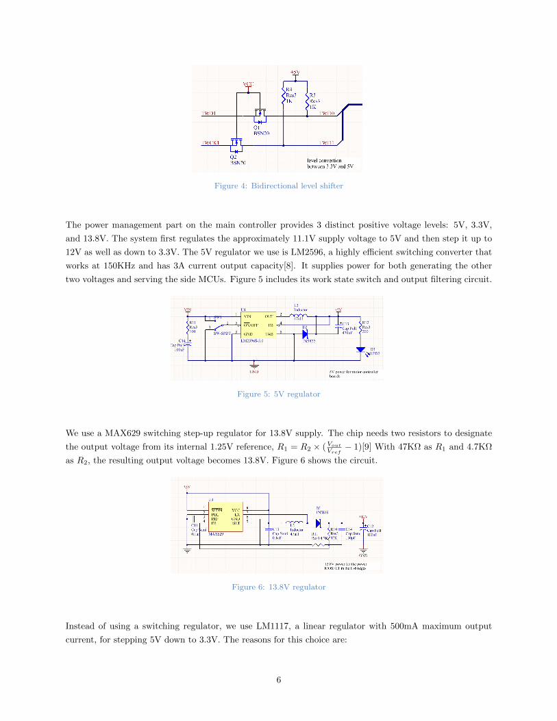
Figure 4: Bidirectional level shifter
The power management part on the main controller provides 3 distinct positive voltage levels: 5V, 3.3V,
and 13.8V. The system first regulates the approximately 11.1V supply voltage to 5V and then step it up to
12V as well as down to 3.3V. The 5V regulator we use is LM2596, a highly efficient switching converter that
works at 150KHz and has 3A current output capacity[8]. It supplies power for both generating the other
two voltages and serving the side MCUs. Figure 5 includes its work state switch and output filtering circuit.
Figure 5: 5V regulator
We use a MAX629 switching step-up regulator for 13.8V supply. The chip needs two resistors to designate
the output voltage from its internal 1.25V reference, R1 = R2 × (Vout
Vref− 1)[9] With 47KΩ as R1 and 4.7KΩ
as R2, the resulting output voltage becomes 13.8V. Figure 6 shows the circuit.
Figure 6: 13.8V regulator
Instead of using a switching regulator, we use LM1117, a linear regulator with 500mA maximum output
current, for stepping 5V down to 3.3V. The reasons for this choice are:
6

1. The 3.3V system consists of the 32-bit MCU, 2.4GHz wireless transceiver, MEMS sensor, and the logic
supply for OLED display, which draw a small total current.
2. The voltage drop from 5V to 3.3V is only 1.7V. Suppose the average current consumption by the 3.3V
system is 100mA, the average dissipation power caused by the voltage drop is 1.7V ×100mA = 170mW ,
which is acceptable.
3. The linear regulator requires much less external components that a switching one does.
Figure 7 presents the circuit.
Figure 7: 3.3V regulator
Since we are using a module integrating the nRF24L01P wireless transceiver, the interface with the wireless
module is just a header. The OLED display takes two voltage supplies: 5V for biasing the display and 3.3V
for powering the logics. It takes data from the main MCU’s SPI interface. Figure 8 shows the circuit.
Figure 8: OLED display
Initially we planed to perform a 9-axis sensor fusion by attaching a 3-axis magnetometer HMC5883L to the
MPU-6050 chip as an auxiliary. The magnetometer is useful for compensating the drift on the gyroscope’s
yaw output by taking reference to the Earth’s magnetic field. However, later we found that the yaw data
are not necessary for the system. As a result, we cut the magnetometer off from the design. Nonetheless, its
place is still kept on the schematic as presented in Figure 9.
7

Figure 9: MEMS sensors
The side controllers use ATmega8A as processors. Besides GPIO (General Purpose Input/Output), we
utilize the MCU’s PWM (Pulse-Width Modulation) generator, external interrupt, and I2C interface. Figure
10 is the core system, including oscillator, power filtering circuit, reset circuit, etc. Because we have totally
4 identical side controllers in the system, in order to apply consistent programs to every chip, we connect
a 4-bit DIP switch to the MCU’s GPIO so that each chip can determine the low 4-bit of its 7-bit I2C
slave upon booting up. The microcontroller is powered up by the 5V that comes from the main controller.
However, each side controller still embeds a LM2596 regulator. The extra 3A current capability provided by
the regulator goes to the 5V DC motor that drives the wheel.
Figure 10: ATmega8A core system
Figure 11 is the design of the H-bridge for driving the worm motors. In the circuit, we use two IR2104
half-bridge chips to provide a 520 nanosecond deadtime to prevent instant short circuit when switching the
direction of the motor. Besides, we also have other circuitry consists of Schottky diodes and resistors that
protects the chips from reverse EMF (ElectroMotive Force). Note that IR2104 requires N-channel MOSFET
instead of typical P-channel ones for the upper arms in the H-bridge. In order to provide the floating VGS for
the NMOS in the upper arms, a bootstrap circuit built from a diode, a Tantalum capacitor, and a charging
resistor, is demanded. In order to charge the capacitor in the bootstrap circuit, we need a certain time of
low level in the driving signal. As a result, the PWM signal provided to the H-bridge cannot reach a 100%
duty cycle; instead, the peak duty cycle is limited at about 95%. The logics on the lower left side of the
figure are responsible to translate the direction and PWM signals into logics that IR2104 accepts. Thanks
to the logics, we are able to generate forward, backward, and breaking commands from two direction inputs
8

Figure 11: H-bridge
The MCU used on the PC side receiver is ATmega32U4. We use two communication modules provided by
the chip: USB for PC communication and SPI for interfacing with the wireless chip. Figure 12 is the core
system of the MCU. Its USB interface is also utilized by a built-in bootloader for programming the chip.
The wireless module on the receiver board is identical to that on the main controller. The receiver board
also has an LM1117 regulator for powering the wireless module up.
Figure 12: ATmega32U4 core system
2.2.2 Software
Because the master controller performs a number of independent tasks, we build the software upon an RTOS
(Real-Time Operating System) to coordinate all the functions. The pre-emptive scheduling provided by the
RTOS ensures high priority tasks to be served in real-time. Table 1 shows a list of tasks that are scheduled.
9

Table 1: RTOS tasks on the master controller
Task function Priority Wake up period
AL system algorithm highest 50ms
Update sensor reading high 10ms
Refresh OLED display low 100ms
Process received command and coordinate the ODM sys-
tem
low 100ms
Send sensor data over wireless low 50ms
System idle task that cleans up dynamic memory and an-
alyzes CPU usage
lowest N/A
Among the tasks, the AL system algorithm has the highest priority. It’s general flowchart is described in
Figure 13.
acquire sensor data
convert quaternions
to Eular angles
tilt angle > 1 degree
wait for new data
lift appropri-
ate wheels
acquire sensor data
tilt angle > 1 degree
set desired angle
to PID controllerwait for new data
yes
no
yes no
Figure 13: General AL system algorithm
10

Although the ODM system has a low priority, it’s still one of the most essential components of the system.
Figure 14 is the mounting coordinates of the servos in the system. The shaded parts in the graph are the
effective angles that the servos can reach, and the numbers at the end points of each half-circle are the
position commands sent to the servo for reaching those angles. In order to keep all the wheels parallel to
each other, a coordinate translation is required for all servos. Imagine that the positive direction on the y
axis in the graph stands for 0 in the whole system; hence, the positive direction on the x axis is 90, and the
negative direction on the y axis is −90. An example of the coordinate translation is also illustrated in the
figure. For the upper right servo, the system coordinate 0 is reinterpreted as 45 in the servo coordinate.
Nonetheless, since each servo can only rotate within 180, the system 180, which is the negative direction
on the y axis, cannot be directly translated into the upper right servo’s coordinate. As a result, we can still
map it to 45 in the servo coordinate and toggle the rotational direction of the corresponding driving wheel.
Any other angle is also able to be translated in the same manner. Therefore, a pseudo 360 coordinates
mapping is done. Table 2 is the complete mapping strategy for all servos. A negative sign at the front stands
for a toggled direction is demanded for the corresponding driving wheel, and the position command sent to
the servo is actually the value within the parentheses. If the calculated result exceeds the upper or lower
limits (±180), the final command should be decreased or increased by 360 respectively.
x
y 45
90
90
−90 90
−90
−90
90 −90
90
Figure 14: Coordinates of the ODM system
Table 2: Servo coordinates mapping strategy
System angle θ Upper left Upper right Lower left Lower right
[−45, 135) N/A 45− θ −(45− θ) N/A
(−180,−45)∪[135, 180] N/A −(−θ − 135) −θ − 135 N/A
[−135, 45) −θ − 45 N/A N/A −(−θ − 45)
(−180,−135)∪[45, 180] −(−θ + 135) N/A N/A −θ + 135
11

In order to achieve maximum performance, all the peripheral and communication module drivers are designed
with non-blocking algorithms.
1. The I2C driver is optimized for RTOS, which means it suspends the calling task when a block read/write
is required and resumes the task after the transaction finishes. This mechanism allows other task to
obtain the CPU resource when a task is waiting for a transaction. The driver also utilizes a DMA
(Direct Memory Access) channel that significantly reduces the CPU load. Furthermore, the fully
automatic streaming algorithm hides the low level interrupt implementation from the RTOS, fulfilling
an OOP (Object Oriented Programming) pattern.
2. The SPI driver also uses a DMA channel as well as a streaming scheme. Besides, the driver packs
the operation mode of the target device into each packet. For instance, the RF chip works at 10MHz
while the OLED is as fast as 33MHz. Therefore, the SPI hardware is able to switch among different
modes autonomously. Different from the I2C driver, the SPI one does not do the RTOS trick. The
reason is that the SPI bus works at high speed comparing to the 400KHz I2C bus; thus, frequent
context switching among tasks may introduce additional overhead. Hence, whether or not to suspend
the calling task has a performance trade off.
The wireless transceiver that we introduce to the project – nRF24L01P – uses a built-in protocol called
Enhanced ShockBurstTM to perform handshaking and error checking so that the MCU can save computing
power for other tasks. The driver for the transceiver embraces the same design idea with the lower level
drivers described above. The driver takes buffers from user and streams them out in a FIFO (First In First
Out) manner. Since the Enhanced ShckBurstTM protocol allows variable length package with maximum
length at 32 bytes[6], if the buffer given by a user has content larger than 32 bytes, the API for appending
package will first recurse to divide the buffer into multiple packages and then add them into the send queue.
The transceiver has two work modes: PTX (Primary Transmitter) and PRX (Primary Receiver), our strategy
is to configure it as PRX when it is idle, and only switch it to PTX when the send queue has packages waiting
to be streamed out. The transceiver has 3 maskable interrupt sources, and uses a pulse on the IRQ pin to
report an interrupt. The sources are: RX DR (RX data ready), TX DS (TX data sent), and MAX RT (TX
maximum retry reached). The driver makes use of all of them, and to handle them as follow:
1. RX DR:
(a) Read the length of the incoming package
(b) Allocate a buffer that fits the length
(c) If the receive queue has too many packages waiting for the user to fetch, then remove and free
the head from the receive queue
(d) Add the incoming package to the tail of the receive queue
2. TX DS:
(a) Check if more packages are in the send queue. If so, continue to send the next package
(b) If not, go to PRX mode
3. MAX RT, this interrupt is triggered when the transmitter loses connection with the receiver, so we
handle it as:
(a) Flush the TX FIFO in the transceiver
(b) Rewrite the last package into the TX payload
12

In contrast to the master controller, the software for the slave ones is relatively simple. It adopts a traditional
foreground-background design, which has an background infinite loop for executing commands and multiple
interrupt service routines as foreground events. As an I2C slave device, the slave controllers follow the I2C
register convention. Table 3 is the list of commands that the controller accept.
Table 3: I2C slave commands
Command
number
Read/write Function
0x01 W Set the PWM output of the driving wheel
0x02 W Set the PWM output of the worm motor
0x03 W Set the position of the servo
0x04 W Set the calibration data to the servo
0x05 W Set the threshold of the saturation filter
0x06 W Break the worm motor
0x07 W Break the driving wheel
0x08 W Give the PID set point to the driving wheel
0xFE R Read the speed of the driving wheel
0xFF R Read the position of the worm motor
When the slave controller receives a command that sets the PID destination of the driving wheel (command
0x08), it loops to execute the control strategy demonstrated in Figure 15 until the error between the set
point and feedback is reduced to a certain range. By tuning the PID constant Kp, Ki, Kd in the figure, the
control scheme finally reaches a 300ms settling time. With this control system, the ODM system is able to
output the same speed to all its 4 wheels, which successfully maintains the heading direction of the whole
vehicle stable.
Ki ×∫ τ0e(τ)dτ
Kp × e(t)
Kd × de(t)dt
Saturation Filter Motor Systemcontroller signal e(t) output
−+
+
Figure 15: Motor control strategy
13

In order to pair with the main controller, the receiver on the PC side also uses an nRF24L01P. Although the
driver for it is also based on stream, it handles the modes differently. Unlike the driver on the AVR32, which
switches to PTX for sending packages, the driver on the receiver side always stays at PRX. When there
are packages ready to send, it utilizes the acknowledgment package specified in the Enhanced ShckBurstTM
protocol to send them[6]. An acknowledgment package is the same with a normal TX package in term of
length; however, it is sent passively when the receiver is acknowledging the transmitter. Therefore, it is never
sent until the link is established between the transmitter and the receiver; thus, the MAX RT interrupt will
never happen under this configuration.
The USB controller in ATmega32U4 has a control endpoint (EP0) with a bank up to 64 byte and 6 other
programmable endpoints. Besides the default EP0, the CDC specification uses other 3 endpoints. One
is used by the CDC class interface, and the other two are used by the data interface. We configure the
endpoints in the AVR as follow:
1. Endpoint 1 is configured in bulk IN mode and has two 64 byte banks in ping-pong mode. It sends the
data from the wireless interface to the PC.
2. Endpoint 2 is configured in bulk OUT mode and has a 32 byte single bank. It receives data from the
PC. The reason not using a 64 byte bank is that 32 byte matches the maximum package size of the
RF chip. This configuration effectively prevents the incoming USB packages from overflow.
3. Endpoint 3 is configured in interrupt IN mode and has a 64 byte single bank. It works as the man-
agement endpoint for the CDC class interface. This endpoint is essentially a dummy one. We do not
need to handle any event from it.
After finish the embedded software, we also need to install the PC driver to test it. Since Windows has a
built-in driver for CDC devices, all we need to do is constructing an .inf file that describes the device. In
order to identify our device, we have to set up the VID (Vendor ID) and PID (Product ID) first. Nonetheless,
applying for valid VID and PID is expensive. Fortunately, ATMEL provides several sets of free VID and
PID for products that uses AVR. The free set for CDC devices are VID=0x16C0 and PID=0x05DF. Figure
16 is a screen shot of the Windows device manager when the receiver is connected.
Figure 16: The Windows device manager identifies the receiver.
Since the receiver is working, we moved on to develop the PC interface software. The resulting GUI (Graphic
User Interface) is shown in Figure 17. The program delivers the following functions so far:
1. Read from the virtual serial port and decode the received data into the real-time roll, pitch, and yaw
information of the vehicle. The low level serial port communication support is provided by a third
party library called QExtSerialPort.
2. Send encoded command to the virtual serial port for controlling the movement of the robot according
the the interaction between the GUI widgets and the operator.
3. Provide intuitive illustration for the incoming data by reflecting the Eular angles on 3D models.
4. Real-time line charts of the data present the trends of the vehicle’s movement.
14
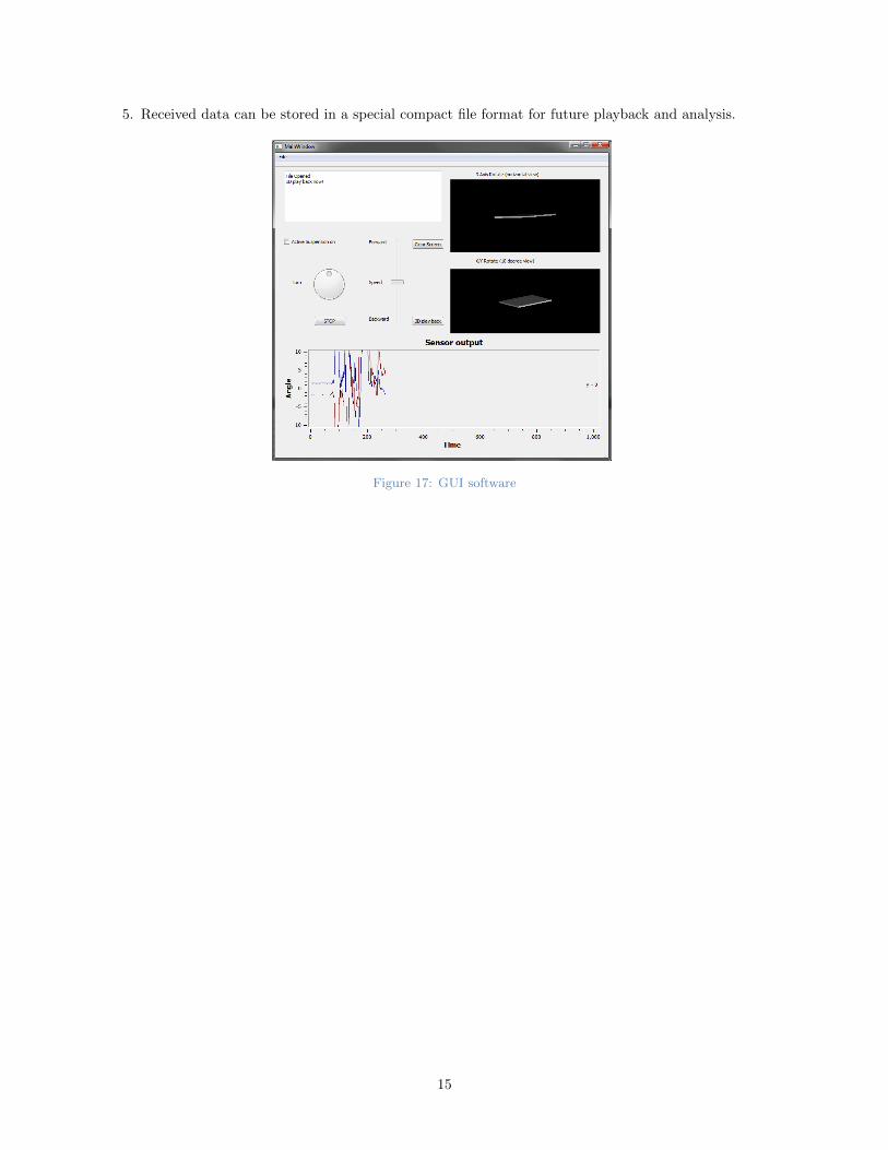
5. Received data can be stored in a special compact file format for future playback and analysis.
Figure 17: GUI software
15

3 Design Verification
This section discusses the general result that the major parts of the system yield. For the full requirements
and verification table, please see the Appendix A.
3.1 Master Controller
The main controller is fully functional according to the verification table. Besides, thanks to the RTOS, we
managed to develop a method to probe the CPU usage of the main processor by counting how much time the
system idle task occupies the CPU comparing to the total time that the CPU runs. Two different counting
methods delivered the ceiling and the floor of the performance. Figure 18 shows the surprising result of the
test: because of the high performance non-blocking asynchronous drivers that we designed, the CPU usage
is as low as around 0.1%∼ 4.6.
1. Performance ceiling: We consider the CPU at idle only when the idle task occupies a whole OS tick
(1ms).
2. Performance floor: We consider the CPU at idle if during an OS tick the idle task is ever resumed.
Figure 18: CPU usage chart
3.2 MEMS Sensors
The MEMS sensor is able to provide roll, pitch and yaw tilt in quaternion format. With its built-in filter,
the results show no pattern of drift and notable noise. The data is verified by keeping the robot still for
a certain period and tracking the sensor reading. After test, we found the standard deviation of total 978
data points is 0.0534, which is satisfying. Furthermore, the long term drift is almost zero in the result chart
(Figure 19). In the plot, the blue trace is the roll reading while the violet one the from pitch. Since the
yaw data are irrelevant to the project, we exclude them from the graph. Conclusively, the sensor output is
robust and credible.
16

Figure 19: MEMS sensor test
3.3 ODM System
The overall ODM system has achieved a stable performance. The PID control system for the driving wheel is
able to keep a 300ms settling time. The servos are calibrated to output the same angle with errors confined
in 5.
3.4 AL System
Due to the mechanical limitation of the worm motor, we could not test the active suspension system of the
vehicle in real world scenarios. However, we still tested the system using software simulation and later proved
that our design is viable. The first verification conducted was to test the settling time of the control system.
The original requirement for it was 50ms. After a careful reconsideration, we changed the requirement to
300ms. Several reasons exist for this change. First, our control feedback sampling period is 50ms, a greater
settling time should be allowed for feedback to become effective. Second, a 50ms settling time will result
in big PID constants, which would make the system unstable by introducing larger overshoot. Last but
not least, a 300ms settling time is quick enough for the system to react. Figure 20 presents the simulation
results. The white signals are randomly generated ramps, and the violet ones shows the system’s reaction.
The graph justifies the quick response rate of the AL algorithm.
Figure 20: AL algorithm simulation
17

4 Cost
4.1 Parts
Table 4: Itemized budget
Part name Unit
cost ($)
Manufacturer Number
required
Subtotal
($)
Actual
Cost ($)
AT32UC3C2256 13.78 ATMEL 1 13.78 13.78
ATmega8A 1.84 ATMEL 4 7.36 7.36
ATmega32U4 3.38 ATMEL 1 3.38 3.38
Worm motor 7 from China 4 28 28
Servo 4 from China 4 16 16
DC motor 4 from China 4 16 16
Encoder 2 from China 4 8 8
Battery 8.2 from China 1 8.2 8.2
nRF24L01P RF module 10.0 Nordic Semiconductor 2 20.0 20.0
MPU-6050 7.14 InvenSense 1 7.14 29.28
IRF3205S 0.42 International Rectifier 16 6.72 6.72
IR2104 0.62 International Rectifier 8 4.96 4.96
MAX629 1.54 MAXIM 1 1.54 0
LM2596S-5.0 0.31 Texas Instrument 4 1.24 0
LM1117-3.3 0.05 Texas Instrument 2 0.10 0.10
LM2594-3.3 1.54 Texas Instrument 1 1.54 1.54
OLED Display 4.92 Univision 1 4.92 4.92
oscillator 0.77 from China 6 4.62 4.62
PCB 20 from China 3 60 60
Misc. components from
China
N/A N/A 5 5
Total 218.5 237.86
4.2 Labor
Machine shop estimation: $1000
Zhangxiaowen Gong: $35/hr × 12hr/week × 10 weeks = $4200
Wenjia Zhou: $35/hr × 12hr/week × 10 weeks = $4200
Jun Ma: $35/hr × 12hr/week × 10 weeks = $4200
Total: $4200 × 3 × 2.5 = $31500
The total expense is $31500 + $237.86 = $1000 = $32737.86
18

5 Conclusion
5.1 Accomplishments and Future Work
We are satisfied with the performance of our vehicle. The ODM system, on-board task management, and
the wireless interface all work flawlessly. Our design has fulfilled most of the requirements and functioned as
expected except that the AL system does not work due to the insufficient torque from the worm motor that
we use. Nonetheless, the simulation results give promising data to justify the AL algorithm. As a result,
a redesign to the physical AL system should deliver successful outcome. A possible alternative approach is
to replace the worm motor with linear actuator. The latter one is slower yet more stable and stronger. We
may also attach a pressure sensor to each driving wheel to examine whether the wheel is firmly touching the
ground so that the measured vehicle state is more credible. In addition, the open-loop controlled RC servos
are hard to be calibrated to output the same angle; hence, we may later adding sensors such as Hall effect
sensors to transform the system into a closed-loop controlled one. Another possible improvement is on the
processor side. Since the CPU usage shows that the main microcontroller is significantly overpowered, we
may also substitute it with a low end ARM Cortex-M3 processor, which may cost only around $3 each.
5.2 Uncertainties
The mechanical part on the small size model system deviates from an actual full size vehicle notably.
Therefore, although we successfully implement the design on the model system, all the parameters in the
control system have to be re-calculated for the real system. Furthermore, an operating system based software
tends to hide subtle synchronization bugs, which may result in hanging the system. For critical operations
like carrying dangerous chemicals, such system failure is intolerable. Consequently, the software has to be
carefully examined to eliminate any of such bugs.
5.3 Ethical considerations
We commit ourselves to the IEEE code of ethics, the ethical concerns we have is as follows:
‘to accept responsibility in making decisions consistent with the safety, health and welfare of
the public, and to disclose promptly factors that might endanger the public or the environment;’
In the case of our project, our design is intended for laboratory use. Nonetheless, we cannot neglect the pos-
sibility that our design is used by unauthorized person or group for transporting unexpected and dangerous
chemical, for instance, any sort of poisons or explosives. If our product is to be used, we will make sure we
only hand it to authorized person or group, and make sure only they know how to operate the system.
19

References
[1] “Omnix Technology, Inc. - Directional Components & Integrated Systems,” Web page, accessed May
2012. [Online]. Available: http://www.omnixtechnology.com/direct components.html
[2] App Note: 9-Axis MotionFusion & Calibration Algorithms, InvenSense Inc., Sunnyvale, CA,
2011. [Online]. Available: http://www.invensense.com/developers/index.php? r=downloads&ajax=
dlfile&file=AppNote%20-%209-Axis%20MotionFusion%20and%20Calibration%20Algorithms.pdf
[3] “IRF3205S IRF3205L,” Datasheet, International Rectifier, 2002. [Online]. Available: http:
//www.irf.ru/pdf/irf3205s.pdf
[4] “Class 1 Bluetooth Dongle Test,” Web page, accessed May 2012. [Online]. Available: http:
//www.amperordirect.com/pc/r-electronic-resource/z-reference-bluetooth-class1-myth.html
[5] IEEE 802.15.4d-2009 IEEE Standard for Information Technology - Specific Requirements – Part 15.4:
Wireless Medium Access Control (MAC) and Physical Layer (PHY) Specifications for Low-Rate
Wireless Personal Area Networks (WPANs), IEEE, New York, NY, 2009. [Online]. Available:
http://standards.ieee.org/getieee802/download/802.15.4d-2009.pdf
[6] “nRF24L01+ Product Specification,” Datasheet, Nordic Semiconductor, 2008. [Online]. Available:
http://www.nordicsemi.com/kor/nordic/download resource/8765/2/23366062
[7] Bi-directional Level Shifter for I2C-bus and Other Systems, Philips Semiconductors, 1997. [Online].
Available: http://ics.nxp.com/support/documents/interface/pdf/an97055.pdf
[8] “LM2596 SIMPLE SWITCHER Power Converter 150 kHz3A Step-Down Voltage Regulator,” Datasheet,
Texas Instrument, 2002. [Online]. Available: http://www.ti.com/lit/ds/symlink/lm2596.pdf
[9] “MAX629 28V, Low-Power, High-Voltage, Boost or Inverting DC-DC Converter,” Datasheet, Maxim
Integrated Products, 1997. [Online]. Available: http://pdfserv.maxim-ic.com/en/ds/MAX629.pdf
20

Appendix A Requirement and Verification Table
A.1 Main Controller
Table 5: Requirement and verification for the main controller
Item Requirement and verification (Y/N) Test/calibration procedure
OLED dis-
play 1. Display characters at spe-
cific coordinates (Y)
1. (a) Command the OLED to display
strings with various lengths at dif-
ferent location
(b) See if all 128 × 64 pixels are opera-
tional
(c) See if all ASCII characters are
mapped to pixels correctly
(d) See if the designated coordinates are
translated to right positions
(e) Check if the strings wrap around
correctly
DSP filter (if
present) 1. Finish each filter compu-
tation within 10ms (Soft-
ware filter is aban-
doned)
2. Filter at least 90% vibra-
tional noise out
1. (a) Turn on the built-in 16-bit T/C
(timer/counter) before starting the
calculation and record the value in
the T/C register right after the
computation finishes
(b) Calculate the delay from the T/C
reading and its clock source setting
2. (a) Send both filtered and raw data to
a computer
(b) Calculate and compare the stan-
dard deviation of each set of data
Continued on next page
21

Table 5 – continued from previous page
Item Requirement and verification (Y/N) Test/calibration procedure
I2C interface
1. Signals have almost verti-
cal edges maximum clock
speed at 400KHz (Y)
2. No malfunction in high-
noise environment (Y)
3. Communication between
3.3V I2C bus and 5V I2C
bus (Y)
4. The streaming algorithm
is able to save over 70%
CPU cycles from simple
synchronous drivers (Y)
1. (a) Set the I2C bus to 400KHz and then
use an oscilloscope to probe the SCL
and SDA lines
(b) Check the edges on the signals and
determine of the curve on the edges,
which are caused by the capacitance
on the trace/wire and the pull-up
resister specified in the I2C stan-
dard, is in an acceptable shape
2. Test the transmission when the H-bridges
and motors are turned on, and see if any
data loss occurs
3. Test the level shifting circuit to see if it
converts signals bidirectionally
4. Loop to append 100 I2C transactions and
see how many packages remain in the
queue after the appending operation is
done; the more packages still stay in the
queue the better the algorithm is
Continued on next page
22

Table 5 – continued from previous page
Item Requirement and verification (Y/N) Test/calibration procedure
SPI interface
1. Internal shift register is
functional (Y)
2. No malfunction in high-
noise environment (Y)
3. When addressing one slave
device, no interference
coming from the others
(Y)
4. Utilize the DMA channel
for both transmitting and
receiving data (Y)
1. Check if the slave data shift to the master
correctly when the master shift its data
out
2. Test the transmission when the H-bridges
and motors are turned on, and see if any
data loss occurs
3. (a) Pull down the chip select lines on
different slaves and see if data go to
correct receiver
(b) Check if the master changes SPI
mode (clock phase, clock polar-
ity, etc.) correctly when switching
among slaves that adopt different
modes
(c) Keep addressing various slaves for
10 minutes and capture any mal-
function
4. (a) Turn on the inner-loop function of
AVR32’s SPI module, which inter-
connect its input to its output
(b) Set one DMA channel to transmit
data in a block of memory
(c) Set the second DMA channel to re-
ceive data and to store them in an-
other block of memory
(d) After the transmission finishes,
check the consistency of the content
in the two memory blocks
23

A.2 MEMS Sensors
Table 6: Requirement and verification for the MEMS sensors
Item Requirement and verification (Y/N) Test/calibration procedure
MPU-6050
1. Be configured with proper
work mode (sensitive
range, interrupt output,
etc.) (Y)
2. Allow the main controller
to configure its auxil-
iary sensor (HMC5883L)
(HMC5883L is aban-
doned)
3. Accelerometer and gyro
scope data are consistent
(Y)
1. (a) Read values from all registers from
the sensors’ register map and check
with the default value stated in
their datasheets
(b) Change values in several registers
and then read back to see if the op-
erations succeed
(c) Move/turn the sensor at certain
rate and check if the output is in
the expected range
2. (a) Use the sensor’s internal MUX to
hand the auxiliary sensor to the
main controller temporarily
(b) Let the main controller to verify if
it can change the auxiliary sensor’s
registers correctly
(c) Get the auxiliary sensor back from
the main controller and try to read
its output
(d) Let the main controller to address
the auxiliary sensor again; the op-
eration should fail now
3. (a) Put sensor unit on the table, tilt a
little bit, and record the output
(b) Calculate θ from accelerometer’s x-
axis (x) and z-axis (z) data: θ =
arctan(−xz )
(c) Calculate γ from gyroscope’s z-axis
(ω) output: γ = ω × t(d) θ should be close to γ
Continued on next page
24

Table 6 – continued from previous page
Item Requirement and verification (Y/N) Test/calibration procedure
HMC5883L
1. Be configured with proper
work mode (gain, in-
terrupt output, etc.)
(HMC5883L is aban-
doned)
2. Error is controlled within
2
1. Perform similar procedure that checks
the MPU-6050
2. (a) Place the sensor on the table and
tilt 45 at a time
(b) Record the output and compare
it to the actual angle; error =
actual − output(c) Repeat the step (a) and (b) until the
total angle tilted reaches 720
(d) Calculate the peak and average of
the errors
A.3 Side Controllers
Table 7: Requirement and verification for the side controllers
Item Requirement and verification (Y/N) Test/calibration procedure
I2C interface
1. Robust communication
with no data loss and
bus errors in high-noise
environment (Y)
2. Multiple side MCUs can
communicate with the
main controller via a single
I2C interface without
suffering bus conflict (Y)
1. Perform the test 1 and 2 in the I2C part
in section 3.1.1
2. (a) Send commands to different slave
MCUs to verify the addressability
(b) Let the main controller keep chang-
ing the slave MCU for 10 minutes and
see if the bus fails in the duration
PWM
1. Generate 3 PWM signals
with different duty cycles
simultaneously (Y)
1. (a) Write a program that generate 3
PWM signals with different duty cy-
cles and changes the duty cycle every
10 seconds
(b) Use 2 oscilloscopes to probe the 3
PWM output pins
(c) Check the correctness of each signal
over time
Continued on next page
25

Table 7 – continued from previous page
Item Requirement and verification (Y/N) Test/calibration procedure
H-bridge
1. Require no heat sink when
driving current stables at
the worm motor’s rated
current, which is 1.10A
(Y)
2. Respond to PWM signals
that have duty cycles rang-
ing from 15% to 95% (Y)
1. (a) Connect an ammeter between the H-
bridge output and the worm motor
(b) Set the H-bridge to output at full
speed (95% duty cycle PWM) and
increase the load on the worm mo-
tor until the ammeter reading reaches
1.10A
(c) Keep the motor spinning for 2 min-
utes
(d) Put on antistatic wrist strap and
feel the temperature on the driving
MOSFET with bare finger; the fin-
ger should not feel hot
2. (a) Set the PWM signal to 15%
(b) Let the H-bridge drive a motor with
no load for 1 minute and see if the
speed is constant
(c) Repeat (a) and (b) with a 10% in-
crease in duty cycle each time untile
the duty cycle reaches 95%
26

A.4 Wireless Communication
Table 8: Requirement and verification for the wireless communication
Item Requirement and verification (Y/N) Test/calibration procedure
nRF24L01P
1. Be configured with proper
work mode (channel, ad-
dress, data rate, etc.) (Y)
2. Communication range is
higher than 100m outdoor
(Y)
3. Communication is not af-
fected if the transceivers
have a wall in between (Y)
1. Perform the test 1 in the MPU-6050 part
in section 3.1.2
2. (a) Put the transmitter and receiver at
the two corners of the Quad
(b) Turn on both transceivers and check
for stable transmission
(c) If fail to establish the data link, hold
the transmitter and walk towards the
receiver until stable data appears
(d) Mark the final locations of the
transceivers on a scaled map and
measure the distance
3. (a) Put the two transceivers in two ad-
jacent rooms and start the transmis-
sion
(b) If the data is stable, move the
transceivers to rooms that have two
walls in between
(c) Increment the number of walls in be-
tween and perform the test until ei-
ther the transmission is blocked of
the number reaches 5
(d) Repeat the test with transceivers
placed in different floors
Continued on next page
27

Table 8 – continued from previous page
Item Requirement and verification (Y/N) Test/calibration procedure
Driver
1. Connect/disconnect au-
tomatically when the
paired transceivers are
in-range/out-of-range (Y)
2. Automatically resend
packages that is not ac-
knowledged by the receiver
(Y)
3. The streaming algorithm
is able to save over 70%
CPU cycles from simple
synchronous drivers (Y)
1. (a) Make the transmitter keep sending
packages
(b) Switch the on/off state of the receiver
several times
(c) See if the link is reestablished auto-
matically
2. In the above test, check if any package is
lost during the off state of the receiver
3. Perform the test 3 in the I2C part in sec-
tion 3.1.1
A.5 Omni-directional Movement
Table 9: Requirement and verification for the omni-directional movement
Item Requirement and verification (Y/N) Test/calibration procedure
DC motor
1. With speed control algo-
rithm, all motor respond
the speed command (0 ∼255) identically (Y)
1. (a) Set the speed commands for all mo-
tors to 50
(b) Use a tachometer to record the speed
of each motor
(c) Repeat (a) and (b) with a 50 increase
in speed command each time until
the command reaches 250
Continued on next page
28

Table 9 – continued from previous page
Item Requirement and verification (Y/N) Test/calibration procedure
Servo
1. All servos respond to posi-
tion commands identically,
which means turning to the
same angle (Y with error
in 5circ)
2. Turn 60 with regular load
within 0.25 second (Y)
1. (a) Set PPM signals equal to the raw po-
sition commands
(b) Set the duty cycle of the raw com-
mand to 2.5% (0.5 millisecond high
level) and provide it to all servos
(c) Record the position of all servos
(d) Repeat (b) and (c) with a 1.0% in-
crease in duty cycle each time until
the duty cycle reaches 12.5% (2.5 mil-
lisecond high level)
(e) Pick one servo as standard, and then
calculate scalar and offset errors of
the other servos according to the re-
sults
(f) Apply proportional and offset fac-
tors to the raw command to gener-
ate modified signals and do (b) to (d)
several times until all servos respond
to the raw command identically
2. (a) Put the vehicle on the table and let
one servo turn 60
(b) Use a video camera with 60fps frame
rate to capture the movement
(c) Playback the video frame by frame
and count the number of frames
taken to finish the turning
(d) Calculate the actual delay in second
by delay = frametaken60
29

A.6 Active Suspension
Table 10: Requirement and verification for the active suspension
Item Requirement and verification (Y/N) Test/calibration procedure
PID algo-
rithm 1. Settling time is controlled
in 50ms (Requirement
changed to 300ms; con-
firmed in simulation)
2. Error between desired an-
gle and actual turned an-
gle is smaller than 2 (Ver-
ified in simulation)
1. (a) Run Simulink in MATLAB and set
the desired angle x as input to the
system
(b) Plot step response in MATLAB
and find the time when the output
reaches 95% of steady state value
(c) Load PID parameter into the vehicle
and run it over a ramp with slope = x
(d) Collect potentiometer reading from
the controller’s ADC (analog to dig-
ital converter), which indicates the
angle turned, and import them to
MATLAB
(e) Mark the delay between the initial
position and the final position by an-
alyzing the data
2. (a) Set 10 as the target angle to the PID
system
(b) Measure the actual turned angle via
a protractor after the system reaches
stable state
(c) Record the error
(d) Repeat from (a) to (c) with a 10 in-
crease in target angle each time until
the target angle reaches 50
30

A.7 PC Receiver
Table 11: Requirement and verification for the PC receiver
Item Requirement and verification (Y/N) Test/calibration procedure
USB inter-
face 1. Both PC side driver and
MCU side driver are func-
tional (Y)
2. Data rate is independent
from the virtual serial
port’s baud rate setting
(Y)
1. (a) Connect the receiver to the PC’s USB
port and see if the PC recognize it
with the name specified in the .inf file
we write
(b) Open the corresponding virtual serial
port in the HyperTerminal
(c) Exchange a group of data and verify
the correctness
2. (a) Set the baud rate of the virtual serial
port to 240bps
(b) Loop to send 1KB of random data to
the PC
(c) Check whether the transmission com-
pletes instantly instead of taking
around 4 seconds
PC software
1. Receive real-time data and
reflect them on line charts
(Y)
2. Store data and time in file
and playback afterwards
(Y)
1. (a) Establish the wireless link between
the vehicle and the PC
(b) Move the vehicle randomly by hand
(c) Check if the line charts correctly dis-
play the movement without recogniz-
able delay
2. (a) Write received data to a non-existed
file and check if the file is created suc-
cessfully in the file system
(b) Open the file and check the consis-
tency with the original data
31
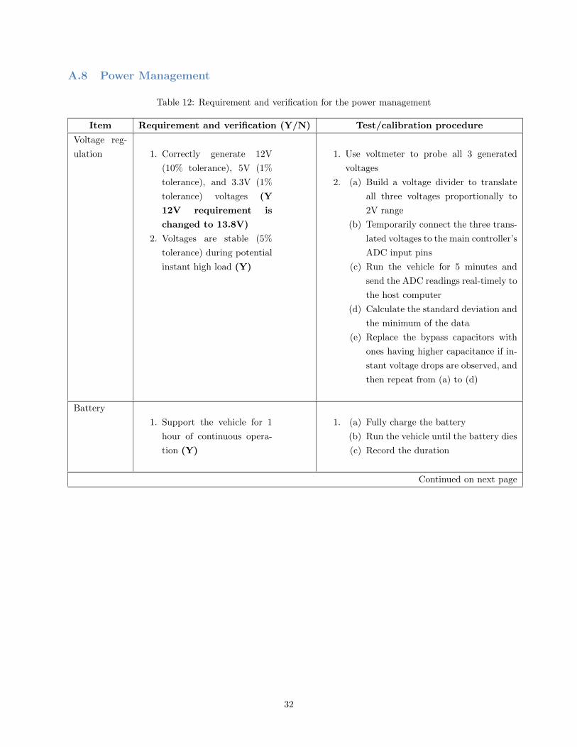
A.8 Power Management
Table 12: Requirement and verification for the power management
Item Requirement and verification (Y/N) Test/calibration procedure
Voltage reg-
ulation 1. Correctly generate 12V
(10% tolerance), 5V (1%
tolerance), and 3.3V (1%
tolerance) voltages (Y
12V requirement is
changed to 13.8V)
2. Voltages are stable (5%
tolerance) during potential
instant high load (Y)
1. Use voltmeter to probe all 3 generated
voltages
2. (a) Build a voltage divider to translate
all three voltages proportionally to
2V range
(b) Temporarily connect the three trans-
lated voltages to the main controller’s
ADC input pins
(c) Run the vehicle for 5 minutes and
send the ADC readings real-timely to
the host computer
(d) Calculate the standard deviation and
the minimum of the data
(e) Replace the bypass capacitors with
ones having higher capacitance if in-
stant voltage drops are observed, and
then repeat from (a) to (d)
Battery
1. Support the vehicle for 1
hour of continuous opera-
tion (Y)
1. (a) Fully charge the battery
(b) Run the vehicle until the battery dies
(c) Record the duration
Continued on next page
32
Table 12 – continued from previous page
Item Requirement and verification (Y/N) Test/calibration procedure
Power con-
sumption 1. Peak current is lower than
6A (Unable to test)
2. Average current is lower
than 2A (Unable to test)
1. (a) Connect a 0.25Ω 10W sensing resister
in the battery loop
(b) Use AVR32’s differential ADC chan-
nel to probe the voltage drop on the
resister
(c) Run the vehicle for 10 minutes and
send the ADC readings real-timely to
the host computer
(d) Find the peak current among the
data
2. In the above test, continue to calculate the
average of all data
33

Appendix B Full Schematics and PCB Layouts
B.1 The Master Controller
34

1
1
2
2
3
3
4
4
D D
C C
B B
A A
Title
Number RevisionSize
Letter
Date: 5/2/2012 Sheet ofFile: F:\Dropbox\..\2.4GHz.Wireless.SchDoc Drawn By:
2.4GHz wireless interface
Zhangxiaowen Gong
CE3
CSN4
SCK5
MOSI6
MISO7
IRQ8
GND1
VCC2RF1
nRF24L01+ board
MOSIMISO
SCKCS
SPI0SPI1
SPI2SPI3
SPI[5..0] SPI[5..0]
CE
VCC
GND
IRQIRQPIRF101
PIRF102
PIRF103
PIRF104
PIRF105
PIRF106
PIRF107
PIRF108
CORF1
PIRF101
PIRF108
NLIRQPOIRQ
PIRF103POCEPIRF102
NLSPI050000POSPI050000
NLSPI050000POSPI050000
POCE
POIRQPOSPI0POSPI1POSPI2POSPI3POSPI4POSPI5POSPI050000

1
1
2
2
3
3
4
4
D D
C C
B B
A A
Title
Number RevisionSize
Letter
Date: 5/2/2012 Sheet ofFile: F:\Dropbox\My.PCBs\ECE445\AVR32.SchDocDrawn By:
PA00(CANIF-TXLINE[1])1
PA01(CANIF-RXLINE[1]/PEVC-PAD_EVT[0])2
PA02(SCIF-GCLK[0]/PEVC-PAD_EVT[1])3
PA03(SCIF-GCLK[1]/EIC-EXINT[1])4
VDDIO1 5
GNDIO1 6
PA04(ADCIN0/USBC-ID/ACIFA0-ACAOUT)7
PA05(ADCIN1/USBC-VBOF/ACIFA0-ACBOUT)8
PA06(ADCIN2/AC1AP1/PEVC-PAD_EVT[2])9
PA07(ADCIN3/AC1AN1/PEVC-PAD_EVT[3])10
PA08(ADCIN4/AC1BP1/EIC-EXINT[2])11
PA09(ADCIN5/AC1BN1)12
PA16(ADCREF0/DACREF)13
ADCVREFP 14
ADCVREFN 15
PA19(ADCIN8/EIC-EXTINT[1])16
GNDANA 17
VDDANA 18
PA20(ADCIN9/AC0AP0/AC0AP or DAC0A)19
PA21(ADCIN10/AC0BN0/AC0BN0 or DAC0B)20
PA22(ADCIN11/AC0AN0/PEVC-PAD_EVT[4]/MACB-SPEED)21
PA23(ADCIN12/AC0BP0/PEVC-PAD_EVT[5]/MACB-WOL)22
VBUS 23DM 24DP 25
GNDPLL 26
VDDIN_5 27
VDDIN_33 28
VDDCORE 29
GNDCORE 30
(XIN0)PB30 31
(XOUT0)PB31 32
PD02(SPI0-SCK/TC0-CLK2/QDEC0-QEPA)49
PD03(SPI0-NPCS[0]/TC0-B2/QDEC0-QEPB)50
VDDIO3 51
GNDIO3 52
PD11(USART1-TXD/USBC-ID/PEVC-PAD_EVT[6]/MACB-TXD[0])53
PD12(USART1-RXD/USBC-VBOF/PEVC-PAD_EVT[7]/MACB-TXD[1])54
PD13(USART1-CTS/USART1-CLK/PEVC-PAD_EVT[8]/MACB-RXD[0])55
PD14(USART1-RTS/EIC-EXINT[7]/PEVC-PAD_EVT[9]/MACB-RXD[1])56
PD21(USART3-TXD/EIC-EXINT[0])57
PD28(USART0-RXD/CANIF-TXLINE[0]/TC0-B0/MACB-RX_DV)59 PD27(USART0-TXD/CANIF-RXLINE[0]/TC0-A0/MACB-RX_ER)58
PD29(USART0-CTS/EIC-EXINT[6]/USART0-CLK/TC0-CLK0/MACB-TX_CLK)60
PD30(USART0-RTS/EIC-EXINT[3]/TC0-A1/MACB-TX_EN)61
PB00(USART0-CLK/CANIF-RXLINE[1]/EIC-EXTINT[8]/PEVC-PAD_EVT[10]/XIN32)62
PB01(CANIF-TXLINE[1]/PEVC-PAD_EVT[11]/XOUT32)63
RESET 64
PC02(TWIMS0-TWD/SPI0-NPCS[3]/USART2-RXD/TC1-CLK1/MACB-MDC)33
PC03(TWIMS0-TWCK/EIC-EXINT[1]/USART2-TXD/TC1-B1/MACB-MDIO)34
VDDIO2 35
GNDIO2 36PC04(TWIMS1-TWD/EIC-EXINT[3]/USART2-TXD/TC0-B1)37
PC05(TWIMS1-TWCK/EIC-EXTINT[4]/USART2-RXD/TC0-A2)38
PC15(PWM-PWMH[1]/SPI0-NPCS[0]/USART0-RXD/CANIF-RXLINE[1])39
PC17(PWM-PWMH[0]/SPI0-NPCS[2]/IISC-ISDO/USART3-TXD)41 PC16(PWM-PWML[1]/SPI0-NPCS[1]/USART0-TXD/CANIF-TXLINE[1])40
PC18(PWM-PWML[0]/EIC-EXINT[5]/IISC-ISDI/USART3-RXD)42
PC19(PWM-PWML[2]/SCIF-GCLK[0]/IISC-IMCK/USART3-CTS)43
PC20(PWM-PWMH[2]/SCIF-GCLK[1]/IISC-ISCK/USART3-RTS)44
PC21(PWM-EXT_FAULTS[0]/CANIF-RXLINE[0]/IISC-IWS)45
PC22(PWM-EXT_FAULTS[1]/CANIF-TXLINE[0]/USART3-CLK)46
PD00(SPI0-MOSI/TC1-CLK0/QDEC0-QEPI/USART0-TXD)47
PD01(SPI0-MISO/TC1-A0/TC0-CLK1/USART0-RXD)48
U1
AT32UC3C2256
VCC
10uH L1
Inductor
NC GNDOUT VDD
Y1
Osc
K2
SW
0.1uF
C6
Cap Semi
0.1uF
C3Cap Semi
0.01uF
C4Cap Semi
1uF
C5Cap Tant
SPI0SPI1SPI2SPI3
SPI4SPI5
MOSIMISOSCKNPCS0
NPCS1NPCS2
SPI[5..0]
TWI00TWI01
TWI10
TWD0TWCK0
TWD1TWCK1TWI0[1..0]
TWI1[1..0]
SPI[5..0]
TWI1[1..0]
TWI0[1..0]
0.1uF
C2Cap Semi
VBUS1 D-2 D+3 ID4 GND5 GND0USB1
Mini USB
22
R2
Res3
22
R3
Res3
UID
UID
K1SW
0.1uF
C1Cap Semi
4.7K
R1Res3
VCC
GND
EXTINT6EXTINT3
EXTINT0
EXTINT0
EXTINT7
EXTINT5
EXTINT8
EXTINT1
EXTINT2
EXTINT8EXTINT1EXTINT2
EXTINT5EXTINT4 TWCK1
EXTINT[8..0] EXTINT[8..0]
Res1-1 1Res2-1 2Res3-1 3Res4-1 4
Res1-28 Res2-27 Res3-26 Res4-25R6
4 Res Pack
TWI00TWI01
VCC
pull-up resisters for TWI pins
pushing during reset will start the bootloader
Zhangxiaowen Gong
AVCC
AVCC
AVR32 microcontroller core system
Q1BSN20
Q2BSN20
+5V
TWCK1
TWD1
VCC
1K
R4Res3
1K
R5Res3
TWD1TWCK1
TWI11
level convertion between 3.3V and 5V
TXDRXD
USART0USART1
USART[1..0]USART[1..0]
0.1uF
C27Cap Semi
0.1uF
C28Cap Semi
PIC101
PIC102COC1
PIC201
PIC202 COC2
PIC301
PIC302 COC3
PIC401
PIC402 COC4 PIC501
PIC502
COC5
PIC601PIC602
COC6
PIC2701
PIC2702 COC27
PIC2801
PIC2802 COC28
PIK101
PIK102
COK1
PIK201PIK202
COK2
PIL101 PIL102
COL1
PIQ101PIQ102 PIQ103
COQ1PIQ201PIQ202 PIQ203
COQ2
PIR101
PIR102
COR1
PIR201 PIR202COR2
PIR301 PIR302
COR3
PIR401
PIR402COR4
PIR501
PIR502COR5
PIR601
PIR602
PIR603
PIR604PIR605
PIR606
PIR607
PIR608
COR6
PIU101
PIU102
PIU103
PIU104
PIU105
PIU106
PIU107
PIU108
PIU109
PIU1010
PIU1011
PIU1012
PIU1013
PIU1014
PIU1015
PIU1016
PIU1017
PIU1018
PIU1019
PIU1020
PIU1021
PIU1022
PIU1023
PIU1024
PIU1025
PIU1026
PIU1027
PIU1028
PIU1029
PIU1030
PIU1031
PIU1032
PIU1033
PIU1034
PIU1035
PIU1036
PIU1037
PIU1038
PIU1039
PIU1040
PIU1041
PIU1042
PIU1043
PIU1044
PIU1045
PIU1046
PIU1047
PIU1048
PIU1049
PIU1050
PIU1051
PIU1052
PIU1053
PIU1054
PIU1055
PIU1056
PIU1057
PIU1058
PIU1059
PIU1060
PIU1061
PIU1062
PIU1063
PIU1064
COU1
PIUSB100
PIUSB101
PIUSB102
PIUSB103
PIUSB104
PIUSB105
COUSB1
PIY100 PIY101
PIY102 PIY103
COY1
PIR402PIR502
PIC202 PIL101
PIU1014
PIU1018NLAVCC
PIC102
PIC201 PIC301
PIC401 PIC502
PIC601
PIC2701
PIC2801
PIK102
PIK201
PIU106
PIU1015
PIU1017
PIU1026
PIU1030
PIU1036
PIU1052
PIUSB100
PIUSB105
PIY101
PIQ103PIR501
NLTWI1010000
NLTWI10
POTWI1010000
PIQ203
PIR401NLTWI1010000
NLTWI11
POTWI1010000
PIR604
PIU1033NLTWD0
NLTWI0010000
NLTWI00
POTWI0010000
PIR603
PIU1034NLTWCK0
NLTWI0010000
NLTWI01
POTWI0010000
PIC402 PIC501PIU1029
PIC602
PIK202PIU1064
PIR201PIU1025 PIR202 PIUSB103
PIR301PIU1024 PIR302PIUSB102
PIU101
PIU102
PIU103
PIU104
PIU108
PIU109
PIU1010
PIU1012
PIU1013
PIU1019
PIU1020
PIU1021
PIU1022
PIU1023 PIUSB101
PIU1031 PIY102
PIU1032
PIU1039
PIU1043
PIU1044
PIU1045
PIU1046
PIU1055
PIU1058
PIU1059
PIU1063
PIY100
PIQ102
PIR602
PIU1037
NLTWD1
PIU107
PIUSB104NLUID
PIC302
PIC2702
PIC2802PIL102
PIQ101
PIQ201
PIR101
PIR605
PIR606
PIR607
PIR608
PIU105
PIU1027
PIU1028
PIU1035
PIU1051
PIY103
PIC101PIK101PIR102
PIU1057
NLEXTINT080000
NLEXTINT0
POEXTINT080000
PIU1016
NLEXTINT080000
NLEXTINT1
POEXTINT080000
PIU1011
NLEXTINT080000
NLEXTINT2
POEXTINT080000
PIU1061
NLEXTINT080000
NLEXTINT3
POEXTINT080000
PIQ202
PIR601
PIU1038
NLEXTINT080000
NLEXTINT4 NLTWCK1
POEXTINT080000
PIU1042
NLEXTINT080000
NLEXTINT5
POEXTINT080000
PIU1060
NLEXTINT080000
NLEXTINT6
POEXTINT080000
PIU1056
NLEXTINT080000
NLEXTINT7
POEXTINT080000
PIU1062
NLEXTINT080000
NLEXTINT8
POEXTINT080000POEXTINT0POEXTINT1POEXTINT2POEXTINT3POEXTINT4POEXTINT5POEXTINT6POEXTINT7POEXTINT8POEXTINT080000
POSPI0POSPI1POSPI2POSPI3POSPI4POSPI5POSPI050000
POTWI00POTWI0010000POTWI01
POTWI1010000POTWI10POTWI11
POUSART0POUSART1POUSART010000

1
1
2
2
3
3
4
4
D D
C C
B B
A A
Title
Number RevisionSize
Letter
Date: 5/2/2012 Sheet ofFile: F:\Dropbox\..\ext.interface.SchDoc Drawn By: Zhangxiaowen Gong
12345
P3
Header 5
12345
P4
Header 5
12345
P6
Header 5
12345
P7
Header 5
+5V+12V
GND
TWI10TWI11
TWI1[1..0] TWI1[1..0]
External interface to motor control boards
USART[1..0] USART[1..0]
USART0USART1
1 2 3
P2
Header 3
123
P5Header 3
PIP201 PIP202 PIP203
COP2
PIP301
PIP302
PIP303
PIP304
PIP305
COP3
PIP401
PIP402
PIP403
PIP404
PIP405
COP4
PIP501PIP502PIP503
COP5
PIP601
PIP602
PIP603
PIP604
PIP605
COP6
PIP701
PIP702
PIP703
PIP704
PIP705
COP7
PIP302
PIP402
PIP602
PIP702
PIP301
PIP401
PIP601
PIP701
PIP303
PIP403
PIP603
PIP703
PIP201
NLTWI1010000
NLTWI10
POTWI1010000PIP503NLTWI1010000
NLTWI11
POTWI1010000
PIP202PIP304
PIP404
PIP604
PIP704
PIP305
PIP405
PIP502
PIP605
PIP705
PIP203NLUSART010000
NLUSART0
POUSART010000
PIP501NLUSART010000
NLUSART1
POUSART010000
POTWI1010000POTWI10POTWI11
POUSART0POUSART1POUSART010000

1
1
2
2
3
3
4
4
D D
C C
B B
A A
Title
Number RevisionSize
Letter
Date: 5/2/2012 Sheet ofFile: F:\Dropbox\..\main.board.SchDoc Drawn By:
TWI0[1..0]TWI1[1..0]
SPI[5..0]
EXTINT[8..0]
USART[1..0]
AVR32 core systemAVR32.SchDoc
SPI[5..0]
D/CRESET
OLEDOLED.SchDoc
TWI0[1..0]
INT
sensorsensor.SchDoc
power managerPM.SchDoc
SPI[5..0]
TWI0[1..0]
EXTINT5
EXTINT[8..0]
EXTINT7
CE
SPI[5..0]
IRQ
wireless2.4GHz.Wireless.SchDoc
EXTINT3EXTINT6
Zhangxiaowen Gong
TWI1[1..0]
USART[1..0]
external interfaceext.interface.SchDoc
TWI1[1..0]
Main sheet
EXTINT2NLTWI1010000NLTWI1010000NLTWI0010000NLTWI0010000
NLEXTINT080000NLEXTINT080000NLEXTINT080000
NLEXTINT2
NLEXTINT080000
NLEXTINT3
NLEXTINT080000NLEXTINT080000
NLEXTINT5
NLEXTINT080000
NLEXTINT6
NLEXTINT080000
NLEXTINT7
NLEXTINT080000
NLSPI050000NLSPI050000NLSPI050000NLSPI050000NLSPI050000NLSPI050000

1
1
2
2
3
3
4
4
D D
C C
B B
A A
Title
Number RevisionSize
Letter
Date: 5/2/2012 Sheet ofFile: F:\Dropbox\My.PCBs\ECE445\OLED.SchDocDrawn By:
SPI[5..0]
D/C
SCKMOSI
SPI2SPI0
CSSPI4
SPI[5..0]
Zhangxiaowen Gong
0.9" OLED display interface
NC(GND) 1
VSS 8
C2P 2
C2N 3
C1P 4
C2N 5
NC 7
VCC 28
BS111
BS212
CS13
D/C15
R/W16
RESET14
VCOMH 27
VBAT 6
D0(SCLK/SCL)18
D1(SDIN/SDAIN)19
D2(SDAOUT)20
D321
D422
D523
D624
D725 IREF 26
NC(GND) 30BS010
VDD 9
E/RD17
VLSS 29
U2
UG-2864HSWEG01
500K
R9
Res3
GND
1uF
C8Cap Semi
1uF
C7Cap Semi
2.2uF
C9
Cap Semi2.2uF
C10Cap Semi
+5V
VCC
Res1-1 1
Res2-1 2
Res3-1 3
Res4-1 4
Res1-28
Res2-27
Res3-26
Res4-25
R8
4 Res Pack
4.7K
R7Res3
RESET
D/CD/C PIC701
PIC702 COC7
PIC801
PIC802 COC8
PIC901PIC902
COC9PIC1001
PIC1002COC10
PIR701
PIR702COR7
PIR801
PIR802
PIR803
PIR804PIR805
PIR806
PIR807
PIR808
COR8
PIR901 PIR902
COR9
PIU201
PIU202
PIU203
PIU204
PIU205
PIU206
PIU207
PIU208
PIU209
PIU2010
PIU2011
PIU2012
PIU2013
PIU2014
PIU2015
PIU2016
PIU2017
PIU2018
PIU2019
PIU2020
PIU2021
PIU2022
PIU2023
PIU2024
PIU2025
PIU2026
PIU2027
PIU2028
PIU2029
PIU2030
COU2PIU206
PIR807
NLD0CPOD0C
PIC901
PIC1002PIR902
PIU201
PIU208
PIU2010
PIU2011
PIU2012
PIU2016
PIU2017
PIU2020
PIU2021
PIU2022
PIU2023
PIU2024
PIU2025
PIU2029
PIU2030
PIC701PIU203
PIC702
PIU202
PIC801PIU205
PIC802PIU204
PIC902PIU2027PIC1001PIU2028
PIR701 PIU2014PORESET
PIR801
PIU2013
PIR802
PIU2015
PIR803 PIU2018
PIR804 PIU2019
PIR901
PIU2026
PIU207
PIR702
PIU209
NLSPI050000POSPI050000 NLSPI050000POSPI050000 NLSPI050000POSPI050000
POD0C
PORESET
POSPI0POSPI1POSPI2POSPI3POSPI4POSPI5POSPI050000

1
1
2
2
3
3
4
4
D D
C C
B B
A A
Title
Number RevisionSize
Letter
Date: 5/2/2012 Sheet ofFile: F:\Dropbox\My.PCBs\ECE445\PM.SchDocDrawn By:
100uF
C16Cap Pol1
470uF
C15Cap Pol1
47uH
L3Inductor
D2
1N5822
100
R12Res3
VIN
GND
+5V
23
1 SW1
SW-SPDT 200
R13Res3
D3LED2
SHDN1
POL2
REF3
FB4
VCC 8
LX 7
GND 6
ISET 5
U3
MAX6290.1uF
C11Cap Semi
0.1uF
C13Cap Semi 47uH
L2Inductor
D11N5819
47K
R10Res3
4.7KR11Res3 150pF
C14Cap Semi 100uF
C12Cap Pol1
GND
+12V
+5V
Zhangxiaowen Gong
GND
15uF
C18Cap Tant
100uF
C17Cap Pol1
+5V
VCC
IN3 OUT 2
GND 1TAB4
U5
LM1117MP-3.3
12
P1
Header 2
VIN
GND
Power management providing +3.3V, +5V, and +12V
13.8V power for the power MOSFET in the H-bridges
5V power for motor controller boards
3.3V power for AVR32, 2.4GHz transceiver, sensor, OLED, etc.
FB 4
VIN1
ON/OFF5
GND3 TAB 6
OUT 2U4
LM2596S-5.0
PIC1101 PIC1102
COC11 PIC1201
PIC1202
COC12
PIC1301
PIC1302COC13
PIC1401
PIC1402COC14
PIC1501
PIC1502COC15
PIC1601
PIC1602
COC16
PIC1701
PIC1702
COC17 PIC1801
PIC1802
COC18
PID101 PID102
COD1
PID201 PID202
COD2
PID301PID302
COD3
PIL201 PIL202COL2
PIL301 PIL302
COL3
PIP101
PIP102
COP1
PIR1001
PIR1002COR10
PIR1101PIR1102
COR11
PIR1201
PIR1202COR12
PIR1301
PIR1302COR13PISW101
PISW102
PISW103
COSW1
PIU301
PIU302
PIU303
PIU304 PIU305
PIU306
PIU307
PIU308
COU3
PIU401 PIU402
PIU403
PIU404PIU405
PIU406
COU4
PIU501
PIU502PIU503
PIU504
COU5
PIC1302
PIC1501
PIC1701
PID202
PIL201
PIL302 PIR1302
PIU301
PIU305
PIU308
PIU404
PIU503
PIC1201PIC1402PID102PIR1002PIC1101
PIC1202PIC1301
PIC1502
PIC1602
PIC1702 PIC1802
PID201
PID302
PIP102
PIR1102
PISW103
PIU302
PIU306
PIU403 PIU406
PIU501
PIC1102PIU303
PIC1401
PIR1001PIR1101
PIU304
PIC1601PIR1201
PID101PIL202
PIU307
PID301PIR1301
PIL301PIU402
PISW102PIU405
PIC1801PIU502
PIU504
PIP101
PIR1202PISW101
PIU401

1
1
2
2
3
3
4
4
D D
C C
B B
A A
Title
Number RevisionSize
Letter
Date: 5/2/2012 Sheet ofFile: F:\Dropbox\My.PCBs\ECE445\sensor.SchDocDrawn By:
GND
VCC
0.1uF
C22Cap Semi
INT
2.2nF
C23Cap Semi
0.1uF
C24Cap Semi
10nF
C21Cap Semi
TWI0[1..0]
TWI00TWI01
TWI0[1..0]
Zhangxiaowen Gong
4.7K
R15Res3
4.7K
R14Res3
6-axis gryoscope and accelerometer interface
S1 4VDDIO 13
SETP8
SETC12
DRDY15
VDD 2
GND 9GND 11
C110
SCL1
SDA16
U6
HMC5883LGND
220nF
C19Cap Semi
4.7uF
C20Cap Tant
HMC5883 works as an auxiliary for MPU-6050's 9-axis sensor fusion
CLKIN1
NC 2NC 3NC 4NC 5
AUX_DA6
AUX_CL7
VLOGIC 8
AD09
REGOUT10
FSYNC11
INT12
VDD 13
NC 14
NC 15
NC 16
NC 17
GND 18
RESV 19
CPOUT20
RESV 21
CLKOUT22
SCL23
SDA24
U7
MPU-6050
0.1uF
C26Cap Semi0.1uF
C25Cap Semi
PIC1901
PIC1902
COC19
PIC2001
PIC2002COC20
PIC2101
PIC2102 COC21
PIC2201
PIC2202 COC22
PIC2301
PIC2302 COC23
PIC2401
PIC2402 COC24
PIC2501
PIC2502 COC25
PIC2601
PIC2602 COC26
PIR1401
PIR1402COR14
PIR1501
PIR1502COR15
PIU601
PIU602
PIU604PIU608
PIU609
PIU6010
PIU6011
PIU6012
PIU6013
PIU6015
PIU6016
COU6
PIU701
PIU702
PIU703
PIU704
PIU705
PIU706
PIU707
PIU708
PIU709
PIU7010
PIU7011
PIU7012
PIU7013
PIU7014
PIU7015
PIU7016
PIU7017
PIU7018
PIU7019
PIU7020
PIU7021
PIU7022
PIU7023
PIU7024
COU7
PIC2002PIC2101 PIC2201
PIC2301 PIC2401
PIC2501PIC2601
PIU609
PIU6011
PIU701
PIU709
PIU7011
PIU7018
PIU7023
NLTWI0010000
NLTWI00
POTWI0010000
PIU7024
NLTWI0010000
NLTWI01
POTWI0010000
PIC1901PIU608PIC1902 PIU6012 PIC2001
PIU6010
PIC2302PIU7020
PIC2402 PIU7010PIR1401PIU601
PIU707
PIR1501PIU6016
PIU706
PIU6015
PIU702
PIU703
PIU704
PIU705
PIU7012POINT
PIU7014
PIU7015
PIU7016
PIU7017
PIU7019
PIU7021
PIU7022 PIC2102 PIC2202PIC2502
PIC2602PIR1402 PIR1502
PIU602
PIU604
PIU6013
PIU708
PIU7013
POINTPOTWI00POTWI0010000POTWI01

PAC101 PAC102
COC1
PAC201PAC202
COC2
PAC301 PAC302
COC3
PAC401 PAC402
COC4
PAC501PAC502COC5
PAC601PAC602
COC6 PAC701PAC702
COC7PAC801PAC802 COC8
PAC901PAC902
COC9
PAC1001PAC1002
COC10
PAC1101PAC1102
COC11
PAC1201 PAC1202
COC12
PAC1301PAC1302COC13
PAC1401 PAC1402COC14
PAC1501
PAC1502
COC15
PAC1601
PAC1602
COC16
PAC1701 PAC1702
COC17
PAC1801PAC1802
COC18
PAC1901PAC1902
COC19PAC2001 PAC2002
COC20
PAC2101 PAC2102
COC21
PAC2201PAC2202
COC22
PAC2301 PAC2302COC23
PAC2401 PAC2402COC24
PAC2501PAC2502COC25
PAC2601PAC2602COC26
PAC2701PAC2702
COC27
PAC2801PAC2802COC28
PAD101
PAD102
COD1PAD201
PAD202
COD2
PAD302
PAD301COD3
PAK102
PAK101
COK1PAK202
PAK201
COK2
PAL102
PAL101COL1
PAL202PAL201
COL2
PAL302PAL301
COL3
PAP102PAP101
COP1
PAP203
PAP202
PAP201
COP2
PAP301PAP302PAP303PAP304PAP305
COP3PAP401PAP402PAP403PAP404PAP405
COP4
PAP503
PAP502
PAP501
COP5PAP601PAP602PAP603PAP604PAP605
COP6PAP701PAP702PAP703PAP704PAP705
COP7
PAQ103
PAQ102
PAQ101
COQ1PAQ203PAQ202
PAQ201
COQ2PAR102PAR101
COR1PAR202 PAR201
COR2
PAR302 PAR301COR3
PAR402PAR401
COR4
PAR502PAR501
COR5
PAR608PAR601PAR602PAR603PAR604
PAR607PAR606PAR605
COR6
PAR701PAR702 COR7PAR808
PAR801 PAR802PAR803 PAR804
PAR807PAR806 PAR805
COR8
PAR901PAR902
COR9
PAR1002PAR1001
COR10
PAR1102PAR1101
COR11PAR1202PAR1201
COR12
PAR1302 PAR1301COR13
PAR1401PAR1402COR14PAR1501PAR1502COR15
PARF100
PARF108
PARF107
PARF106
PARF105
PARF104
PARF103
PARF102
PARF101
CORF1
PASW101 PASW102 PASW103COSW1
PAU101PAU102PAU103PAU104PAU105PAU106PAU107PAU108PAU109PAU1010PAU1011PAU1012PAU1013PAU1014PAU1015PAU1016
PAU1017PAU1018PAU1019PAU1020PAU1021PAU1022PAU1023PAU1024PAU1025PAU1026PAU1027PAU1028PAU1029PAU1030PAU1031PAU1032PAU1033PAU1034PAU1035PAU1036PAU1037PAU1038PAU1039PAU1040PAU1041PAU1042PAU1043PAU1044PAU1045PAU1046PAU1047PAU1048
PAU1049PAU1050PAU1051PAU1052PAU1053PAU1054PAU1055PAU1056PAU1057PAU1058PAU1059PAU1060PAU1061PAU1062PAU1063PAU1064COU1
PAU2029 PAU2030PAU2027 PAU2028PAU2025 PAU2026PAU2023 PAU2024PAU2021 PAU2022PAU2019 PAU2020PAU2017 PAU2018PAU2015 PAU2016PAU2013 PAU2014PAU2011 PAU2012PAU209 PAU2010PAU207 PAU208PAU205 PAU206PAU203PAU204PAU202PAU201
COU2
PAU305
PAU306
PAU307
PAU308
PAU304
PAU303
PAU302
PAU301
COU3PAU406PAU405PAU404PAU403PAU402PAU401
COU4
PAU504PAU503
PAU502
PAU501
COU5
PAU601PAU602PAU603PAU604PAU605PAU606PAU607PAU608
PAU609PAU6010PAU6011PAU6012PAU6013PAU6014PAU6015PAU6016COU6
PAU701PAU702PAU703PAU704PAU705PAU706
PAU707PAU708PAU709PAU7010PAU7011PAU7012PAU7013PAU7014PAU7015PAU7016PAU7017PAU7018
PAU7019PAU7020PAU7021PAU7022PAU7023PAU7024
PAU7025
COU7
PAUSB100
PAUSB105PAUSB104
PAUSB103
PAUSB102PAUSB101
COUSB1
PAY101
PAY102PAY103
PAY100
COY1
PAC1302
PAC1501
PAC1701
PAD202
PAL201PAL302
PAP302
PAP402
PAP602
PAP702
PAR402
PAR502
PAR1302
PAU206
PAU301
PAU305
PAU308
PAU404
PAU503
PAC1201
PAC1402
PAD102
PAP301
PAP401
PAP601
PAP701
PAR1002
PAC202
PAL101PAU1014
PAU1018
PAC101PAK101
PAR102
PAU1057
PAU1016
PAR701
PAU1011
PAU2014
PARF103
PAU1061PAQ202
PAR601PAU1038
PAU1042
PAU7012
PARF108
PAU1060
PAR807
PAU1056PAU1062
PAC102
PAC201
PAC301
PAC401PAC502
PAC601
PAC901 PAC1002
PAC1101
PAC1202
PAC1301
PAC1502
PAC1602
PAC1702
PAC1802
PAC2002
PAC2101
PAC2201
PAC2301PAC2401
PAC2501
PAC2601PAC2701
PAC2801
PAD201 PAD302
PAK102
PAK201
PAP102
PAP303
PAP403
PAP603
PAP703
PAR902
PAR1102
PARF101
PASW103
PAU106
PAU1015
PAU1017 PAU1026 PAU1030
PAU1036
PAU1052
PAU201 PAU208 PAU2010 PAU2011 PAU2012 PAU2016 PAU2017 PAU2020 PAU2021 PAU2022 PAU2023 PAU2024 PAU2025 PAU2029 PAU2030
PAU302
PAU306
PAU403
PAU406
PAU501
PAU609PAU6011
PAU701
PAU709 PAU7011
PAU7018
PAUSB100
PAUSB105
PAY101
PAC402PAC501
PAU1029
PAC602
PAK202
PAU1064
PAC701
PAU203
PAC702
PAU202
PAC801
PAU205
PAC802
PAU204
PAC902
PAU2027
PAC1001
PAU2028
PAC1102 PAU303
PAC1401PAR1001
PAR1101
PAU304PAC1601 PAR1201
PAC1901PAU608
PAC1902PAU6012 PAC2001PAU6010
PAC2302
PAU7020
PAC2402
PAU7010
PAD101PAL202
PAU307 PAD301PAR1301
PAL301
PAU402
PAP202
PAP304
PAP404
PAP604
PAP704
PAP305
PAP405
PAP502
PAP605
PAP705
PAR201
PAU1025
PAR202PAUSB103
PAR301
PAU1024
PAR302PAUSB102
PAR801
PAU2013
PAR802
PAU2015
PAR803
PAU2018
PAR804
PAU2019
PAR901
PAU2026
PAR1401 PAU601
PAU707
PAR1501PAU6016
PAU706
PASW102
PAU405
PAU1023
PAUSB101
PAU1031
PAY102
PAR805PARF106
PAU1047
PARF107
PAU1048
PAR806
PARF105
PAU1049
PARF104
PAU1050
PAR808
PAU1040PAU1041
PAR603PAU1034
PAU7024
PAR604PAU1033
PAU7023
PAQ102
PAR602PAU1037
PAP201
PAQ103 PAR501
PAP503
PAQ203 PAR401
PAU107
PAUSB104
PAP203PAU1053
PAP501
PAU1054
PAC302
PAC1801
PAC2102
PAC2202
PAC2502
PAC2602
PAC2702
PAC2802
PAL102
PAQ101
PAQ201
PAR101
PAR605PAR606PAR607PAR608
PAR702
PAR1402PAR1502
PARF102
PAU105
PAU1027PAU1028
PAU1035
PAU1051
PAU209
PAU502PAU504
PAU602 PAU604
PAU6013
PAU708PAU7013
PAY103
PAP101
PAR1202
PASW101
PAU401

B.2 The Slave Controllers
35
1
1
2
2
3
3
4
4
D D
C C
B B
A A
Title
Number RevisionSize
Letter
Date: 5/2/2012 Sheet ofFile: F:\Dropbox\..\AVR8.SchDoc Drawn By:
PWM1
0.1uF
C2Cap Semi
VCC
0.1uF
C3Cap Semi
ADDR0ADDR1ADDR2ADDR3
NCGNDOUTVDD
Y1
Osc
XIN
XIN
GND
VCC
PWM0
PWM2
K1SW
0.1uF
C1Cap Semi
4.7K
R2
Res3
VCC
GND
SDASCL
TWI0TWI1
TWI[1..0]TWI[1..0]
INT0INT1
INT[1..0] INT[1..0] DIR0DIR1
DIR3
PWM[2..0] PWM[2..0]
DIR2
DIR3
DIR[3..0] DIR[3..0]
1234
8765
S1
SW DIP-4
ADDR[3..0]
ADDR0ADDR1ADDR2ADDR3
ADDR[3..0]GND
LED0
LED1
VM
200
R4
Res3
200
R3
Res3
D2
LED2
D1
LED2
LED0
LED1
ADC
Zhangxiaowen Gong
AVR8 microcontroller core system
DIP switch that determines the low bits of the TWI address
MISOMOSISCK
RST
VCC
GND
SCK
RST
MISO
PWM2
USART[1..0]
USART0USART1
USART[1..0]
PC6 (RESET) 29PD0 (RXD)30
PD1 (TXD)31
PD2 (INT0)32
PD3 (INT1)1
PD4 (XCK/T0)2
VCC 6
GND 5
PB6 (XTAL1/TOSC1)7
PB7 (XTAL2/TOSC2)8
PD5 (T1)9
PD6 (AIN0)10
PD7 (AIN1)11
PB0 (ICP)12
PB1 (OC1A)13
PB2 (SS/OC1B)14
PB3 (MOSI/OC2)15
PB4 (MISO)16
PB5 (SCK)17
AVCC 18
AREF 20
GND 21
PC0 (ADC0) 23
PC1 (ADC1) 24
PC2 (ADC2) 25
PC3 (ADC3) 26
PC4 (ADC4/SDA) 27
PC5 (ADC5/SCL) 28
GND 3
VCC 4
ADC6 19
ADC7 22
U1
ATmega8-16AI
VM
4.7K
R1
Res3
1 23 45 6
P1
Header 3X2
PIC101
PIC102COC1
PIC201
PIC202COC2
PIC301
PIC302COC3
PID101 PID102
COD1
PID201 PID202
COD2
PIK101
PIK102
COK1
PIP101 PIP102
PIP103 PIP104
PIP105 PIP106
COP1
PIR101 PIR102
COR1
PIR201 PIR202
COR2
PIR301PIR302COR3
PIR401PIR402
COR4
PIS101
PIS102
PIS103
PIS104PIS105
PIS106
PIS107
PIS108
COS1
PIU101
PIU102
PIU103
PIU104
PIU105
PIU106
PIU107
PIU108
PIU109
PIU1010
PIU1011
PIU1012
PIU1013
PIU1014
PIU1015
PIU1016
PIU1017
PIU1018
PIU1019
PIU1020
PIU1021
PIU1022
PIU1023
PIU1024
PIU1025
PIU1026
PIU1027
PIU1028
PIU1029PIU1030
PIU1031
PIU1032
COU1
PIY100PIY101
PIY102PIY103
COY1
PIC102
PIC201PIC301
PIK102
PIP106
PIS101
PIS102
PIS103
PIS104
PIU103
PIU105
PIU1021
PIY101
PID102
PIU108
NLLED0
PID202
PIU102
NLLED1
PIP101
PIU1016
NLMISO
PID101PIR301
PID201PIR401
PIR101PIU1022
PIU1019 POADC
PIY100
PIC101PIK101
PIP105
PIR201PIU1029
NLRSTPIP103
PIU1017
NLSCK
PIC202PIC302
PIP102
PIR202
PIU104
PIU106
PIU1018
PIU1020
PIY103
PIR102
PIR302
PIR402
PIU107
PIY102NLXIN
PIS108
PIU1023
NLADDR030000
NLADDR0
PIS107
PIU1024
NLADDR030000
NLADDR1
PIS106
PIU1025
NLADDR030000
NLADDR2
PIS105
PIU1026
NLADDR030000
NLADDR3
PIU109
NLDIR030000
NLDIR0
PODIR030000
PIU1010
NLDIR030000
NLDIR1
PODIR030000
PIU1011
NLDIR030000
NLDIR2
PODIR030000
PIU1012
NLDIR030000
NLDIR3
PODIR030000
PIU1032
NLINT010000
NLINT0
POINT010000
PIU101
NLINT010000
NLINT1
POINT010000
PIU1013
NLPWM020000
NLPWM0
POPWM020000
PIU1014
NLPWM020000
NLPWM1
POPWM020000
PIU1030
NLUSART010000
NLUSART0
POUSART010000
PIU1031
NLUSART010000
NLUSART1
POUSART010000
POADC
PODIR0PODIR1PODIR2PODIR3PODIR030000
POINT0POINT1POINT010000
POPWM0POPWM1POPWM2POPWM020000
POTWI0POTWI1POTWI010000
POUSART0POUSART1POUSART010000

1
1
2
2
3
3
4
4
D D
C C
B B
A A
Title
Number RevisionSize
Letter
Date: 5/2/2012 Sheet ofFile: F:\Dropbox\..\H-bridge.SchDoc Drawn By:
VCC1
COM4
VB 8HO 7
VS 6
LO 5
IN2
SD3
U2
IR2104S
VCC 1
COM 4
VB8 HO7
VS6
LO5
IN 2
SD 3
U3
IR2104S
M
B1
Motor
Q1IRF3205S
Q3IRF3205S
Q2IRF3205S
Q4IRF3205S
GND
D8D Schottky
D10D Schottky
D7D Schottky
D9D Schottky
1K
R9
Res3
1K
R11
Res3
1K
R10
Res3
1K
R12
Res3
1K
R7
Res3
1K
R14
Res31K
R13
Res3
1K
R6
Res3
D3
Diode 1K
R5
Res3
D4
Diode1K
R8
Res3
100pF
C10Cap Semi
100pF
C9Cap Semi
VIN
89 10
U4CMC74HC00AD
1112
13
U4D
MC74HC00AD
56
4U4B
MC74HC00AD
1
23
U4A
MC74HC00ADGND
+12V D6D Schottky
D5D Schottky
D11D Schottky
D12D Schottky
100pF
C7Cap Tant
+12V
VIN
GND
100pF
C11
Cap Semi
1000uF
C6Cap Pol1
100pF
C8Cap Tant
1000uF
C4Cap Pol1
1000uF
C5Cap Pol1
DIR0PWM
DIR1
Zhangxiaowen Gong
H-bridge DC motor driver
VCC VDD
PIB101 PIB102
COB1
PIC401
PIC402
COC4 PIC501
PIC502
COC5 PIC601
PIC602
COC6
PIC701 PIC702COC7
PIC801PIC802COC8
PIC901
PIC902COC9
PIC1001
PIC1002 COC10
PIC1101PIC1102
COC11
PID301 PID302
COD3
PID401PID402
COD4
PID501PID502
COD5
PID601PID602
COD6
PID701PID702
COD7
PID801 PID802
COD8
PID901PID902
COD9
PID1001 PID1002
COD10
PID1101PID1102
COD11
PID1201PID1202
COD12
PIQ101
PIQ102
PIQ103
COQ1
PIQ201
PIQ202
PIQ203
COQ2
PIQ301
PIQ302
PIQ303COQ3
PIQ401
PIQ402
PIQ403 COQ4
PIR501 PIR502COR5
PIR601 PIR602COR6
PIR701 PIR702COR7
PIR801 PIR802COR8
PIR901 PIR902
COR9PIR1001 PIR1002
COR10
PIR1101 PIR1102
COR11PIR1201 PIR1202
COR12
PIR1301 PIR1302
COR13PIR1401 PIR1402
COR14
PIU201
PIU202
PIU203
PIU204 PIU205
PIU206
PIU207
PIU208
COU2
PIU301
PIU302
PIU303
PIU304PIU305
PIU306
PIU307
PIU308
COU3
PIU401
PIU402
PIU403
COU4A
PIU404
PIU405
PIU406
COU4B
PIU408
PIU409 PIU4010
COU4C
PIU4011
PIU4012
PIU4013
COU4D
PIC902 PIC1002
PID301 PID401
PIU201 PIU301
PIC402 PIC502 PIC602
PIC901 PIC1001
PID1101 PID1201
PIQ303 PIQ403
PIU204 PIU304
PIU401
PIU402
PIU407
PIB101
PIC702
PIC1102
PID501
PID1102
PIQ103PIQ302PIU206 PIB102
PIC802
PIC1101
PID601
PID1202
PIQ203PIQ402 PIU306
PIC701
PIR502
PIU208 PIC801
PIR801
PIU308
PID302PIR501 PID402PIR802
PID701PIR901PID702
PIR601
PIU207
PID801PIR1002 PID802
PIR702
PIU307
PID901PIR1101PID902
PIR1301
PIU205
PID1001PIR1202 PID1002
PIR1402
PIU305
PIQ101
PIR602
PIR902 PIQ201
PIR701
PIR1001
PIQ301PIR1102
PIR1302
PIQ401PIR1201
PIR1401
PIU202
PIU404PIU408
PIU203 PIU303
PIU406
PIU302
PIU405
PIU4011
PIU403
PIU409PODIR0
PIU4010PIU4012POPWM
PIU4013PODIR1
PIU4014
PIC401 PIC501 PIC601
PID502 PID602PIQ102 PIQ202
PODIR0
PODIR1
POPWM

1
1
2
2
3
3
4
4
D D
C C
B B
A A
Title
Number RevisionSize
Letter
Date: 5/2/2012 Sheet ofFile: F:\Dropbox\..\Interface.SchDoc Drawn By:
12345
P5
Header 5
VCC +12V
GND
123456
P7
Header 6
1234
P8
Header 4
123
P10
Header 3GND
SERVO
DIR1DIR0
PWM
VM
GND GND
ENCODER
Zhangxiaowen Gong
Interface with motor, servo, and main controller
VM
5V RC servo interface
feedback from DC motor
DC motor with intrgrated H-bridge
interface with the main controller
TWI0TWI1
TWI[1..0] TWI[1..0]
USART[1..0] USART[1..0]
USART0USART1
1 2 3
P4
Header 3
123
P6Header 3
123
P9
Header 3
ADC
VCC
GND
PIP401 PIP402 PIP403
COP4
PIP501
PIP502
PIP503
PIP504
PIP505
COP5
PIP601PIP602PIP603
COP6
PIP701
PIP702
PIP703
PIP704
PIP705
PIP706
COP7
PIP801
PIP802
PIP803
PIP804
COP8
PIP901
PIP902
PIP903
COP9
PIP1001
PIP1002
PIP1003
COP10
PIP501
PIP503
PIP706 PIP804
PIP903
PIP1003
NLGNDPIP402PIP504
PIP505
PIP602
PIP703PODIR0PIP704PODIR1PIP705POPWM
PIP801 POENCODERPIP802
PIP803
PIP902POADC
PIP1001POSERVO
PIP502
PIP901
PIP701
PIP702
PIP1002NLVM
PIP401
NLTWI010000
NLTWI0
POTWI010000PIP603NLTWI010000
NLTWI1
POTWI010000
PIP403NLUSART010000
NLUSART0
POUSART010000
PIP601NLUSART010000
NLUSART1
POUSART010000
POADC
PODIR0PODIR1
POENCODER
POPWM
POSERVO
POTWI0POTWI1POTWI010000
POUSART0POUSART1POUSART010000

1
1
2
2
3
3
4
4
D D
C C
B B
A A
Title
Number RevisionSize
Letter
Date: 5/2/2012 Sheet ofFile: F:\Dropbox\..\motor.controller.SchDoc Drawn By:
TWI[1..0]
PWM[2..0]
ADC
DIR[3..0]INT[1..0]
USART[1..0]
AVR8 core systemAVR8.SchDoc
DIR0DIR1PWM
H-bridgeH-bridge.SchDoc
Power managementPM.SchDoc
Zhangxiaowen Gong
Main sheet
DIR0DIR1PWM0
DIR[3..0]PWM[2..0]
TWI[1..0]
PWMDIR0DIR1ENCODER
SERVO
USART[1..0]ADC
InterfaceInterface.SchDoc
TWI[1..0]
INT0
PWM1
DIR2DIR3
PWM2
INT[1..0]
USART[1..0]
NLDIR030000
NLDIR0
NLDIR030000
NLDIR1
NLDIR030000
NLDIR2
NLDIR030000
NLDIR3
NLINT010000
NLINT0
NLINT010000
NLPWM020000
NLPWM0
NLPWM020000
NLPWM1
NLPWM020000
NLPWM2
NLTWI010000NLTWI010000
NLUSART010000NLUSART010000

1
1
2
2
3
3
4
4
D D
C C
B B
A A
Title
Number RevisionSize
Letter
Date: 5/2/2012 Sheet ofFile: F:\Dropbox\..\PM.SchDoc Drawn By:
100uF
C13Cap Pol1
470uF
C12Cap Pol1
47uH
L1Inductor
D13
1N5822
100
R15Res3
VIN
GND
23
1 SW1
SW-SPDT 200
R16Res3
D14LED2
Zhangxiaowen Gong
12
P3
Header 2
VIN
GND
Power management providing +5V
FB 4
VIN1
ON/OFF5
GND3 TAB 6
OUT 2U5
LM2596S-5.0
VM
5V 3A power for both servo and DC motor
12
P2
Header 2
VIN
GND
PIC1201
PIC1202
COC12
PIC1301
PIC1302
COC13
PID1301 PID1302
COD13
PID1401PID1402
COD14
PIL101 PIL102
COL1
PIP201
PIP202
COP2PIP301
PIP302
COP3
PIR1501
PIR1502COR15
PIR1601
PIR1602COR16PISW101
PISW102
PISW103
COSW1 PIU501 PIU502
PIU503
PIU504PIU505
PIU506
COU5
PIC1202
PIC1302
PID1301
PID1402
PIP202 PIP302
PISW103
PIU503 PIU506
PIC1301PIR1501
PID1401PIR1601
PIL101PIU502
PISW102PIU505
PIP201 PIP301
PIR1502PISW101
PIU501
PIC1201
PID1302
PIL102 PIR1602PIU504

PAB102
PAB101
COB1
PAC101PAC102
COC1
PAC202PAC201COC2
PAC302PAC301COC3
PAC401
PAC402
COC4
PAC501
PAC502
COC5
PAC601
PAC602
COC6
PAC701 PAC702COC7
PAC801 PAC802COC8
PAC901 PAC902
COC9
PAC1001 PAC1002COC10
PAC1101 PAC1102COC11
PAC1202
PAC1201COC12 PAC1301
PAC1302
COC13
PAD102
PAD101
COD1PAD202
PAD201
COD2
PAD301 PAD302COD3
PAD401 PAD402COD4
PAD502
PAD501
COD5PAD602
PAD601
COD6
PAD701PAD702COD7
PAD801PAD802COD8
PAD901PAD902
COD9
PAD1001PAD1002COD10
PAD1102
PAD1101COD11
PAD1202
PAD1201COD12
PAD1301
PAD1302
COD13
PAD1402PAD1401COD14
PAK102 PAK101
COK1
PAL102 PAL101COL1
PAP101PAP102
PAP103PAP104
PAP105PAP106
COP1
PAP201
PAP202COP2
PAP302
PAP301
COP3
PAP403
PAP402
PAP401
COP4PAP501PAP502PAP503PAP504PAP505
COP5
PAP603
PAP602
PAP601
COP6
PAP706
PAP705
PAP704
PAP703
PAP702
PAP701
COP7
PAP801
PAP802
PAP803
PAP804
COP8PAP903
PAP902
PAP901
COP9
PAP1003
PAP1002
PAP1001
COP10
PAQ101
PAQ102PAQ103
COQ1
PAQ201
PAQ202PAQ203
COQ2PAQ301
PAQ302PAQ303
COQ3
PAQ401
PAQ402PAQ403
COQ4
PAR101 PAR102
COR1
PAR202PAR201
COR2
PAR302 PAR301COR3
PAR402PAR401
COR4
PAR502PAR501
COR5
PAR602PAR601COR6
PAR702 PAR701
COR7PAR802 PAR801
COR8
PAR902PAR901COR9
PAR1002 PAR1001
COR10
PAR1102PAR1101COR11
PAR1202 PAR1201
COR12
PAR1302PAR1301COR13
PAR1402 PAR1401
COR14
PAR1502PAR1501
COR15
PAR1602
PAR1601COR16
PAS105
PAS106
PAS107
PAS108
PAS104
PAS103
PAS102
PAS101
COS1
PASW101 PASW102 PASW103COSW1
PAU1032PAU1031PAU1030PAU1029PAU1028PAU1027PAU1026PAU1025
PAU1024PAU1023PAU1022 PAU1021 PAU1020PAU1019PAU1018PAU1017PAU1016PAU1015PAU1014PAU1013PAU1012PAU1011PAU1010PAU109
PAU108PAU107PAU106PAU105PAU104PAU103PAU102PAU101COU1 PAU201
PAU202
PAU203
PAU204
PAU208
PAU207
PAU206
PAU205
COU2
PAU301
PAU302
PAU303
PAU304
PAU308
PAU307
PAU306
PAU305
COU3
PAU401
PAU402
PAU403
PAU404
PAU405
PAU406
PAU407
PAU4014
PAU4013
PAU4012
PAU4011
PAU4010
PAU409
PAU408
COU4
PAU506PAU505 PAU504 PAU503 PAU502 PAU501
COU5
PAY101
PAY102PAY103
PAY100
COY1PAC902
PAC1002
PAD301
PAD401
PAP501
PAU201
PAU301
PAS108
PAU1023PAS107 PAU1024PAS106 PAU1025
PAS105PAU1026
PAU109
PAU409
PAU1010PAU4013
PAP703
PAU1011
PAP704
PAU1012
PAC102
PAC201
PAC301
PAC402 PAC502 PAC602
PAC901
PAC1001
PAC1202
PAC1302PAD1101 PAD1201
PAD1301
PAD1402
PAK102PAP106
PAP202
PAP302
PAP503
PAP706
PAP804
PAP903
PAP1003
PAQ303 PAQ403
PAS101
PAS102
PAS103
PAS104
PASW103
PAU103 PAU105
PAU1021
PAU204
PAU304
PAU401
PAU402
PAU407
PAU503
PAU506
PAY101
PAP801
PAU1032
PAU101
PAD102
PAU108
PAD202
PAU102
PAP101PAU1016
PAB101PAC702
PAC1102
PAD501PAD1102
PAQ103
PAQ302
PAU206
PAB102
PAC802
PAC1101
PAD601 PAD1202
PAQ203
PAQ402PAU306
PAC701PAR502
PAU208
PAC801PAR801
PAU308
PAC1301PAR1501
PAD101PAR301
PAD201PAR401
PAD302PAR501
PAD402PAR802
PAD701PAR901PAD702PAR601
PAU207
PAD801PAR1002PAD802PAR702
PAU307
PAD901PAR1101PAD902PAR1301
PAU205
PAD1001PAR1202PAD1002PAR1402
PAU305
PAD1401PAR1601
PAL101
PAU502
PAP402
PAP504PAP505
PAP602
PAP902
PAU1019
PAQ101
PAR602PAR902
PAQ201
PAR701PAR1001
PAQ301
PAR1102
PAR1302
PAQ401
PAR1201PAR1401
PAR101
PAU1022
PASW102
PAU505
PAU202
PAU404
PAU408PAU203
PAU303
PAU406
PAU302
PAU405
PAU4011
PAU1013
PAU4010
PAU4012
PAP1001
PAU1014
PAP104
PAP705
PAU1015
PAC101PAK101PAP105
PAR201
PAU1029
PAP103PAU1017
PAP401
PAU1027
PAP603PAU1028
PAP403
PAU1030
PAP601
PAU1031
PAC202
PAC302
PAP102
PAP502
PAP901
PAR202
PAU104 PAU106
PAU1018PAU1020
PAU4014
PAY103
PAC401 PAC501 PAC601
PAD502 PAD602
PAP201
PAP301
PAQ102 PAQ202
PAR1502
PASW101
PAU501PAC1201
PAD1302
PAL102
PAP701
PAP702 PAP1002
PAR102
PAR302PAR402
PAR1602
PAU504
PAU107
PAY102

B.3 The PC Receiver
36

1
1
2
2
3
3
4
4
D D
C C
B B
A A
Title
Number RevisionSize
A4
Date: 5/2/2012 Sheet ofFile: F:\Dropbox\..\Main.Sheet.SchDoc Drawn By:
PE6(INT.6/AIN0)1
UVcc2
D-3
D+4
UGnd5
UCap6
VBus7
PB0(SS/PCINT0)8
PB1(PCINT1/SCK)9
PB2(PDI/PCINT2/MOSI)10
PB3(PDO/PCINT3/MISO)11
PB7(PCINT7/OC0A/OC1C/RTS)12 RESET 13
VCC14
GND 15
XTAL2 16XTAL1 17
PD0(OC0B/SCL/INT0)18
PD1(SDA/INT1)19
PD2(RXD1/INT2)20
PD3(TXD1/INT3)21
PD5(XCK1/CTS)22
GND 23
AVCC24
PD4(ICP1/ADC8) 25PD6(T1/OC4D/ADC9) 26PD7(T0/OC4D/ADC10) 27PB4(PCINT4/ADC11) 28PB5(PCINT5/OC1A/OC4B/ADC12) 29PB6(PCINT6/OC1B/OC4B/ADC13) 30PC6(OC3A/OC4A) 31PC7(ICP3/CLK0/OC4A) 32PE2(HWB) 33
VCC34
GND 35
PF7(ADC7/TDI) 36PF6(ADC6/TDO) 37PF5(ADC5/TMS) 38PF4(ADC4/TCK) 39PF1(ADC1) 40PF0(ADC0) 41
AREF42
GND 43
AVCC44
U1
ATmega32U4
VBUS 1
D- 2
D+ 3
ID 4
GND 5
GND 0
USB1
Mini USB
IN3 OUT 2
GND 1TAB4
U2
LM1117IMP-3.3GND
15uF
C6Cap Tant
3.3V
VBUS
1uF
C4
Cap Tant
GND
22
R1
Res3
22
R2
Res3
10uF
C2Cap Pol1
F1
Fuse 1
VCC
GNDVBUS
VCC
VCC
10uF
C1Cap Pol1
NC GNDOUT VDD
Y1
Osc
VCC
GND
RST
IRQ
MOSI
CSNCE
SCK
MISO
3.3V
MISOMOSISCK
CSNCEIRQ
K1SW
10K
R4Res3
VCC
0.1uF
C7Cap Semi
RST
HWB
HWB
K2SW
10K
R5Res3
VCC
0.1uF
C8Cap Semi
123456
P1
Header 6
MISOMOSI
SCK
RST
VCC
GNDLED0
200
R3Res3
D1LED2
VCC
CE3
CSN4
SCK5
MOSI6
MISO7
IRQ8
GND1
VCC2RF1
nRF24L01+ boardGND
LED0
0.1uF
C5Cap Semi
0.1uF
C3Cap Semi
Zhangxiaowen Gong
USB interfaced 2.4GHz transceiverreset and bootloader activator
3.3V power for 2.4GHz transceiver
8-bit AVR with USB 2.0 controller
PIC101
PIC102COC1 PIC201
PIC202COC2
PIC301
PIC302COC3
PIC401PIC402
COC4
PIC501
PIC502COC5
PIC601
PIC602COC6
PIC701
PIC702COC7
PIC801
PIC802COC8
PID101PID102
COD1
PIF101 PIF102
COF1
PIK101
PIK102
COK1PIK201
PIK202
COK2
PIP101
PIP102
PIP103
PIP104
PIP105
PIP106
COP1
PIR101 PIR102
COR1
PIR201 PIR202
COR2
PIR301
PIR302COR3
PIR401
PIR402COR4
PIR501
PIR502COR5
PIRF101
PIRF102
PIRF103
PIRF104
PIRF105
PIRF106
PIRF107
PIRF108
CORF1
PIU101
PIU102
PIU103
PIU104
PIU105
PIU106
PIU107
PIU108
PIU109
PIU1010
PIU1011PIU1012 PIU1013
PIU1014
PIU1015
PIU1016
PIU1017
PIU1018
PIU1019
PIU1020
PIU1021
PIU1022
PIU1023
PIU1024
PIU1025
PIU1026
PIU1027
PIU1028
PIU1029
PIU1030
PIU1031
PIU1032
PIU1033
PIU1034
PIU1035
PIU1036
PIU1037
PIU1038
PIU1039
PIU1040
PIU1041
PIU1042
PIU1043
PIU1044
COU1
PIU201
PIU202PIU203
PIU204
COU2
PIUSB100
PIUSB101
PIUSB102
PIUSB103
PIUSB104
PIUSB105
COUSB1
PIY100 PIY101
PIY102 PIY103
COY1
PIC601
PIRF102
PIU202
PIU204
PIRF103
PIU1018NLCE
PIRF104
PIU1012NLCSN
PIC102 PIC202 PIC301
PIC402
PIC501PIC602
PIC701 PIC801PIK102 PIK202
PIP106PIRF101
PIU105
PIU1015
PIU1023
PIU1035
PIU1043
PIU201
PIUSB100
PIUSB105
PIY101
PIC802PIK201
PIR501
PIU1033
NLHWB
PIRF108
PIU1019NLIRQ
PID102
PIU108
NLLED0
PIP103
PIRF107
PIU1011NLMISO
PIP104
PIRF106
PIU1010NLMOSI PIY100
PIUSB104 PIU1041
PIU1040
PIU1039
PIU1038
PIU1037
PIU1036
PIU1032
PIU1031
PIU1030
PIU1029
PIU1028
PIU1027
PIU1026
PIU1025
PIU1022
PIU1021
PIU1020
PIU1017 PIY102
PIU1016
PIU101
PIR202 PIU104PIR201PIUSB103
PIR102 PIU103PIR101PIUSB102
PID101PIR301
PIC401PIU106
PIC702PIK101
PIP105
PIR401
PIU1013
NLRST
PIP102PIRF105
PIU109NLSCK
PIC101PIF101
PIUSB101
PIC201 PIC302
PIC502
PIF102
PIP101
PIR302PIR402 PIR502
PIU102
PIU107
PIU1014
PIU1024
PIU1034
PIU1042
PIU1044
PIU203
PIY103
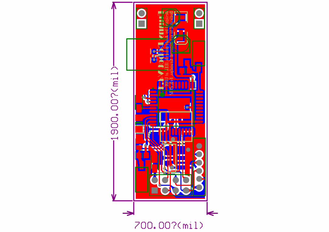
PAC102 PAC101
COC1
PAC202
PAC201COC2
PAC301 PAC302COC3
PAC402PAC401
COC4 PAC501 PAC502COC5
PAC602PAC601
COC6PAC702PAC701
COC7
PAC802PAC801
COC8
PAD101
PAD102
COD1
PAF102
PAF101
COF1
PAK101
PAK102
COK1
PAK201
PAK202COK2
PAP101PAP102PAP103PAP104PAP105PAP106
COP1
PAR101PAR102
COR1
PAR201PAR202
COR2
PAR301 PAR302COR3
PAR401 PAR402
COR4
PAR501PAR502COR5
PARF101
PARF102
PARF103
PARF104
PARF105
PARF106
PARF107
PARF108
PARF100
CORF1
PAU101PAU102PAU103PAU104PAU105PAU106PAU107PAU108PAU109PAU1010PAU1011
PAU1012PAU1013 PAU1014 PAU1015 PAU1016 PAU1017PAU1018PAU1019PAU1020 PAU1021 PAU1022PAU1023PAU1024PAU1025PAU1026PAU1027PAU1028PAU1029PAU1030PAU1031PAU1032PAU1033
PAU1034PAU1035PAU1036PAU1037PAU1038PAU1039PAU1040PAU1041PAU1042PAU1043PAU1044
COU1
PAU201
PAU202
PAU203
PAU204
COU2
PAUSB101
PAUSB102
PAUSB103
PAUSB104
PAUSB100
PAUSB105
COUSB1
PAY101
PAY102 PAY103
PAY100
COY1
PAC601PARF102
PAU202PAU204
PARF103
PAU1018
PARF104
PAU1012
PAC102
PAC202
PAC301
PAC402PAC501
PAC602
PAC701
PAC801
PAK102
PAK202
PAP106
PARF101
PAU105
PAU1015PAU1023
PAU1035PAU1043
PAU201
PAUSB100
PAUSB105
PAY101
PAC802PAK201PAR501
PAU1033
PARF108
PAU1019
PAD102 PAU108
PAP103
PARF107
PAU1011
PAP104
PARF106
PAU1010
PAC401 PAU106
PAD101PAR301
PAR101 PAUSB102PAR102
PAU103
PAR201PAUSB103
PAR202
PAU104
PAU1017
PAY102
PAC702
PAK101PAP105PAR401
PAU1013
PAP102
PARF105
PAU109
PAC101PAF101
PAUSB101
PAC201
PAC302
PAC502
PAF102
PAP101
PAR302
PAR402
PAR502
PAU102
PAU107
PAU1014
PAU1024
PAU1034PAU1042PAU1044
PAU203
PAY103