sop receiver kit - new jersey qrp clubnjqrp.club/sop/sop manual rev b.pdfsop receiver kit assembly...
TRANSCRIPT

SOP Receiver Assembly Manual, rev B 1
New Jersey
SOP Receiver Kit
Brought to you by the New Jersey QRP Clubhttp://www.njqrp.org
A “universal” CW receiver for 80m and 40m operation.Easy to modify for use on other bands. Direct conver-sion for simplicity and performance. Low current drainfrom 9V-12V battery is perfect for portable operation.Open pc board layout - perfect for novice homebrewers,great for experimenting. Add-on accessories: FreqMiteaudio frequency dial, homebrew copper-clad enclosure,all controls, knobs & jacks.

2 SOP Receiver Assembly Manual, rev B
About this manual ...This manual actually consists of five separate manuals combinedinto a single and convenient reference manual for the NJQRP SOPReceiver.
SECTION 1: SOP Receiver -- Covers theory of operation, assembly,debug and operation of the base SOP Receiver kit ................ page 3
SECTION 2: “FreqMite” Audio Frequency Annunciator -- Covers theassembly and operation of the optional “audio frequency dial”components kit ..................................................................... page 22
SECTION 3: “Homebrew Enclosure” -- Covers assembly andfinishing of the optional pcb enclosure kit ............................ page 26
SECTION 4: “Controls & Hardware” -- Covers the assembly of theoptional kit providing components that are external to the pc board:potentiometers and jacks ..................................................... page 39
SECTION 5: Test and Measurement Circuits -- Provides schematicsand guidance for usage of various circuits useful in constructing anddebugging the SOP Receiver .............................................. page 41
Copyright 2000, George Heron, N2APB and the New Jersey QRP Club.All rights reserved.
Edited and published by N2APB, using Pagemaker v6.Printed by Sir Speedy Printing in Baltimore, Maryland.

SOP Receiver Assembly Manual, rev B 3
SOP Receiver KitAssembly Manual
The SOP is a basic “Seat Of the Pants” receiver designed by veteranelmer Joe Everhart, N2CX, and is being kitted and sold by the NJQRPClub. This kit is a very flexible and inexpensive direct conversion CWreceiver for 40m or 80m. Providing better quality than a single-chipreceiver, yet not as complex as a superhet, the SOP’s straightforwarddesign and construction is ideal for newcomers to the homebrewingscene as well as for experienced QRP builders.
WELCOME!Thanks for purchasing the SOP ReceiverKit from the NJQRP Club. This sectionof the manual provides a basic technicaloverview of the design and operation, anddetails the assembly required to make it afunctional receiver in your shack.
The SOP (Seat-Of-the-Pants) is intendedas a utility CW receiver, useful in theshack to complement some of the simpletransmitter projects available today (TunaTin 2, Fireball 40, etc.); or for use in thefield because of its low power consump-
tion and small size.
It uses a simple direct conversion tech-nique and is well-suited for experimen-tation. Though designed originally as acompanion to the NJQRP Fireball-40transmitter, it is a “natural” to team upwith any simple QRP transmitter. An-other use is that of band monitoring. TheSOP provides an elegant way to listen toa band wherever you might be.
The SOP incorporates an audio low passfilter to minimize off-frequency interfer-ence but by design is not so selective that

4 SOP Receiver Assembly Manual, rev B
nearby signals cannot be heard. Whilesuperheterodyne receivers offer betterperformance, the SOP’s simplicity makesit easier to tune up on anywhere in theHF spectrum for CW (or SSB) reception.
An important concept to keep in mind isthat the SOP is an experimenter’s re-ceiver. The building blocks used in thedesign are simple and straightforward,providing a clear functional representa-tion of a relatively generic receiver plat-form. Thus the SOP is a perfect receiverplatform with which to try out new ideas.
The printed circuit board for the SOP issimilarly generous in size to provide nov-ice fingers ample space to assemble andfor oscilloscope probes and extra com-ponents to be connected. The functionalblocks of the design are arranged in amanner to allow easy modification andsubstitution of components. In fact, onecould easily provide little “daughterboards” to sit directly above any particu-lar module to replace or augment its func-tion. For example, if a better audio filteris desired (more poles, different rolloffcharacteristics, etc), one could create a 1”x 1” board containing the improved filterand suspend it above the stock filter onthe middle-right end of the board,jumpering the input and output signalsdown to the original board. Great flex-ibility is provided in the SOP in this man-ner.
The SOP Receiver was designed for flex-ibility. Again, with the basic no-frillscomponent construction, the design canbe easily modified for use on other bands.Application notes will be available in thenear future describing the changes nec-essary to put the receiver on any HF hamband, from 10m to 160m.
The SOP is not necessarily the highest-performing receiver you can find. But forits low cost, it will provide you manyhours of quality service as a flexible re-
ceiver in the shack, as well as being a plat-form for you to modify and improve onas your needs and skills develop.
In the process of assembling your SOPand in modifying it to suit your particu-lar needs, you will gain a better under-standing of the principles of receivers,including oscillators, mixers, RF and au-dio amplification, and audio filtering.
We hope you enjoy your SOP Receiverkit!
MINI-SPECSHere is a brief listing of the SOPreceiver’s specifications. See Figure 1 fora corresponding block diagram.
1) The SOP is a “universal” HF CWreceiver;- Low current drain; able to operate from9V battery or 12V source;- Small size enables use as custom rig oras standalone portable monitor receiver;- Jumper selectable operation on 80m or40m;- Can be set up on any other HF band(30m-10m) with few component changes;- No critical assembly or alignment re-quired;- Tailorable for advanced homebrewers -extra pcb space provided for experimen-tation;- No odd-ball crystals, variable capaci-tors or other components;- Plug and play design ideal for begin-ners or advanced homebrewers;- Solid repeatable design;- Open layout on PC board simplifiesconstruction.
2) The RF Amp- Provides front end gain and selectivity;- Very stable grounded gate FET design;- Provides adequate gain and enhancesnoise figure on higher HF bands;- Can be tailored to any HF band via par-allel inductor or capacitor (pcb space pro-

SOP Receiver Assembly Manual, rev B 5
vided).3) The Local Oscillator- Simple, trouble-free VXO design pro-vides variable tuning control;- Uses ceramic resonator for 80m & 40moperation, easily placed anywhere onband with alternate resonator/crystal;- Tuning range is > 50 KHz on 80m, and> 100 KHz on 40m, ensuring coverageof the standard QRP operating frequen-cies on each band;- Tuning range can be limited simply bychanging padding resistors;- Can use other crystal or resonator tocover any HF band on 80m to 10m;- Output tank is shielded inductor - elimi-nates fragile trimmer capacitors;- Output tank tailored to any HF band viaparallel inductor or capacitor (pcb spaceprovided);- Varactor tuning via potentiometer elimi-nates need for big, expensive variablecapacitor.
4) The LO buffer- Stable, repeatable design provides high-level drive to mixer stage for improvedperformance;- No adjustments;- Broadband performance.
5) The Mixer- Single-chip, passive double balancedmixer (dbm);- No diode matching or toroid winding,yet all the benefits of discrete dbm per-formance;- Better performance in crowded HFbands than single IC mixers;- Simple wide-band termination on out-put helps reject interference.
6) The Audio Stage- Low noise bipolar amplifier providesamplification and filtering;- Integrated circuit audio filter helps withcw reception;- Low pass filter peaked for CW tones;- No adjustments;- No ringing or ear fatigue;
- Filters out high frequency “monkeychatter”.
7) The Audio Muting and Amplifier- Proven muting design quiets receiveraudio during transmit via keyline signalfrom transmitter;- Bypass resistor on muting switch allowsoperator to hear sidetone of the transmit-ted signal;- Allows verification of transmit fre-quency offset;- Proven LM386 amplifier features highfrequency hiss rejection;- Anti motorboat components give cleanaudio output;- Sufficient output for low impedanceheadphones or small speaker.
CIRCUIT OVERVIEWFigure 2 shows the SOP’s schematic.
RF Pre-AmpThe SOP RF amplifier is a single-stagecommon-gate FET stage that providesfront-end gain and selectivity for the re-ceiver. The antenna input is link-coupledto a tuned circuit to provide impedancematching which preserves circuit Q whileefficiently coupling receive energy. Reso-nance at 7 MHz is achieved by use of a150 pF trimmer capacitor, allowing “on-frequency” tuneup. The transformerwinding instructions can be scaled toother amateur bands as well. Energy fromthe tank is coupled to the FET source viaa two-turn tap. Not that both the inputlink and output tap are 2 turns providingidentical input and output matching. Theinput impedance of the grounded gateamplifier is in the range of 50 to 100 ohmsso a reasonable match is achieved.
Source resistor R11 is used to provide anegative gate bias to stabilize FET op-eration with a source current of severalmilliamperes. The FET would probablygive more gain without the resistor, butbias current would vary widely with de-

6S
OP
Rec
eive
r A
ssem
bly
Man
ual,
rev
B
oo
o
oo oo
o
oo
Low-noiseMPF-102RF pre-amp
Space foroptional T-Rswitch parts
Low-costADE-1 dbm.More crunch-proof than ‘602
Low-noisebuffer/amp~20dB gain
Pre-tuned 4-pole Low Pass Filter
Keyline mutesRx audio during TxBypass resistor provides sidetone
T-R A=32N3565 LM 358
Key(Mute)
Audio ampto drive ‘phonesor small speaker
LM 386
SA-612 based Local Osc80m or doubled to 40mOptional components easily added for 30m thru 10m
Stable pot-tunedVXO with varactorand resonator
LO2-stage buffer/ampprovides highinjection levels to mixer
DoubleBalancedMixer
Audio Frequency Annunciation (optional)“Freq-Mite” from Small Wonder Labsannounces operating frequency in Morsecode through receiver headphones.
Freq-Mite
Figure 1 - SOP Receiver Block Diagram

SOP Receiver Assembly Manual, rev B 7
vice-to-device tolerances. Gain stabilityis more important than raw gain. Capaci-tor C15 provides a low-impedance bypassacross the R11 to prevent signal loss. Thecommon gate configuration provides asmall voltage gain with a low noise fig-ure. The low noise is not too important atthe low end of the HF spectrum but willaid ultimate receiver sensitivity on 20meters and higher. An additional advan-tage of the common gate stage is that it isquite stable and repeatable, thus requir-ing no neutralization or tricky adjust-ments.
Output selectivity and matching areachieved via a common 10.7 MHz IFtransformer. It is resonated on 30 metersand below by means of an external ca-pacitor. On 20m and above, an externalcapacitor and inductor do the job. Linkcoupling steps down the high FET drainimpedance to the 50 ohm level requiredby the ADE-1 balanced mixer. Tuningadjustment is done by the variable induc-tance of the shielded transformer. Tun-ing is rather broad since the transformeris heavily loaded by the following doublebalanced mixer.
MixerOne of the most important areas of theSOP is the mixer. A Mini-Circuits ADE-1 double-balanced diode mixer is used.This device is a surface mount packagedequivalent of two small toroid transform-ers surrounding a ring of four diodes. Itprovides good sensitivity while givingmuch less audio rectification than themore common NE602 Gilbert cell mixerused in other direct-conversion receivers.(The NE602 has been recently been su-perseded by the SA612 so from here onout we will use the latter part number.)R12 and C18 provide a wide-band termi-nation to the ADE-1 mixer.
The Local OscillatorThe SOP uses an SA612 to provide thelocal oscillator signal for the mixer. This
device incorporates both an oscillator anda mixer in an 8-pin package — this dualfunctionality is used to good advantage.The “stock” SOP uses a 3.58 MHz ce-ramic resonator in a voltage controlledoscillator to tune a portion of the 80 meterband. The resonator has a lower Q thanthat of a quartz crystal so it can be tunedover a wider range while still being morestable than an LC circuit. The fundamen-tal oscillator output is used for 80 meteroperation. However if the oscillator sig-nal is fed to the SA612 mixer section, itis doubled in frequency to 40 meters. Atuned circuit on the SA612 output mini-mizes 80 meter feedthrough. The receivercan then be used on 40 meters by retun-ing the RF amplifier to that band.
This “trick” works well for 80 and 40meters because of the inexpensive reso-nator. Unfortunately there are no standardunits available on other ham bands. How-ever the SA612 can be set on other bandsby using quartz crystals in place of theresonator. Tuning range can be enhancedby using the “super VXO” techniques ofadding a series inductance and parallel-ing multiple crystals. Naturally the RFamplifier must be retuned to the band ofinterest. Application notes will soon bemade available showing how to effec-tively modify the basic 80m/40m SOP foruse on other bands.
The Local Oscillator is tuned by provid-ing a variable DC voltage to a varactordiode. The TUNE potentiometer providesa portion of the regulated 6V DC levelcoming from the 3-terminal voltage regu-lator U2. C16 and R10 bypass the DCcontrol signal to keep RF from gettinginto the tuning components. Whenvaractor diode D3 sees a range of DC biasvoltage applied, its characteristic capaci-tance changes and adds to the total ca-pacitance in the Y1 resonator circuit. Thisvarying capacitance “bends” the effectivefrequency of the oscillator, providing the

8 SOP Receiver Assembly Manual, rev B
range of frequencies under control of theoperator.
The TUNE potentiometer is padded by aresistor on each end. R7 and R8 can be ajumper wire (i.e., zero ohms) to providethe widest swing of DC control voltage,and thus the widest swing of frequenciesfrom the oscillator. However this mightbe too course an adjustment for some, soa smaller tuning range can be forced byplacing actual in position at R7 and R8,thus providing a smaller range of controlvoltage for the same 300-degree turn ofthe pot. This will have the effect of pro-viding “bandspread-like” operation andgive the operator finer tuning control,making it easier to tune closely-spacedstations.
LO BufferThe Local Oscillator Buffer is comprisedof the Q1 and Q2 stages immediately fol-lowing the LO. Transistor Q1 is config-ured as an emitter follower to serve as ahigh impedance buffer to minimize load-ing of the LO. Transistor Q2 is a com-mon emitter amplifier with a wide-bandtransformer to provide a low impedanceoutput (50-ohms) to drive the mixer stage.By constructing T1 as a trifilar-woundtoroid transformer, we have an easy wayto achieve the wide-band impedancetransformation. R30, C10 and C37decouple the buffer amplifier from the restof the circuits on the +V power line andthus reduce the chance for feedback toand from the power bus. (Direct-conver-sion receivers are very sensitive to cross-coupling through common power busconnections.)
Audio GainThe ADE-1 audio output is boosted by alow-noise 2N3565 transistor amplifier.As in all direct conversion receivers mostof the gain is produced at audio frequen-cies. The mixer output is carefully filteredby C36 to prevent RF feed-through. If youdon’t do this, strong AM signals will be
rectified in the audio amplifier! Again,DC power to the audio amp is carefullyfiltered by R19 and C34 to minimize feed-back from other stages.
Low Pass FilterA low-Q low pass filter is peaked in the700-800 Hz area to give some audio se-lectivity but mainly to filter out off-fre-quency signals. This design originatedwith Wes Hayward some years ago andhas been detailed in a number of publica-tions and articles. Probably the most com-mon reference is the ARRL “Solid StateDesign for the Radio Amateur” by Hay-ward and DeMaw.
This unity gain amplifier and filter is di-rect-coupled — the same voltage appearsat R15/R16 junction, and at the op ampoutput pins 1 and 7. C22 and C25 areNPO-type capacitors for good frequencystability of the filter. C23 and C25 arealso important for frequency stability, buthere we use mylar capacitors for a costeffective solution.
MutingMuting of the receiver is required during“key down” times in order to keep thevery strong signal from blasting out theaudio amp output stage when the localtransmitter is keyed. This clever mutingcircuit, borrowed from Hayward andLewellan, uses the key line signal from acompanion transmitter to switch off anFET to reduce audio levels during trans-mission. However when the key line isclosed and the FET is turned off (its gatewill be negative with respect to itssource), some audio signal is still pro-vided through R23 to produce a ready-made sidetone for the operator.
Audio AmpThe SOP uses the ubiquitous LM386 inthe audio output stage. This device hassufficient drive for headphones; a loud-speaker can also be used in a quiet roomwhen receiving strong signals.

SOP Receiver Assembly Manual, rev B 9
R13 and R25 keep the FreqMite audioannunciator from being affected by thesetting of the AUDIO LEVEL potenti-ometer.
R26 and C29 serve to decouple the am-plifier from the power bus. This preventsthe strong output signals of the LM386from getting back to other componentsin the receive chain.
C30 sets the amplifier to the maximumavailable gain. C31 provides low imped-ance DC decoupling. R27 and C32 pro-vide feedback to lessen high frequencyhiss in the audio output. R28 and C33dampen the output of the amplifier tominimize high frequency oscillation andinstability.
CONSTRUCTIONHere are the steps to follow in puttingyour SOP Receiver Kit together. Referto the Parts List on the next page for adescription of each part in the kit.
1. Parts InventoryCheck out the contents of your kit to en-sure that all parts are present. As youidentify each component, put a littlecheckmark next to that line item, or writethe number of components you count upfor the lines containing multiple parts ofthe same value.
The most of integrated circuits (ICs) andtransistors will be found pushed into ananti-static foam pad.
The mixer integrated circuit (U3) is a“surface mount device”, or SMD. It iscontained in a little 1/4” x 1/4” squareplastic container with a clear plastic cover.We’ll describe how to mount this whenthe time comes, but don’t worry about itright now ... it’s a piece of cake!
2. Other Things NeededYou’ll need some common tools andthings normally found on the workbench.
Soldering tools: A fine-tipped, low-watt-age soldering iron will be important tohave available. Ideally, a temperature-controlled solder station has been foundto be of great service to manyhomebrewers and kit builders. I’ve foundthat setting the tip temperature to about650-degrees works best. Use of a wet pador rag for wiping the tip just before sol-dering a component lead keeps the tipclean and free of oxidation and carboncrud. A supply of standard 60/40 solderfrom Radio Shack (p/n 64-009) will workjust fine. And finally, to clean up the in-evitable solder shorts, many builders havehad great success using SolderWick, abraided wire to help soak up the solderbridges when heated.
The basic tools needed in putting to-gether a kit such as this include fine-pointneedle nose pliers, wire (side) cutters, asmall-blade screwdriver for adjusting theIF transformer cans, and an Exacto bladefor general probing around and scrapingoff the insulation from the magnet wireswhen making the transformers. Other,more elaborate tools can be useful but arenot required. These might include twee-zers for holding very small parts, “thirdhand” device for holding the board atvarious angles, and a lighted magnifyingglass .
Connecting wire: About 5” of thin gaugehook up wire will be needed for the singlejumper on the board. And you’ll needsome additional wire to connect your fa-vorite controls and jacks to the board. In-dividual wires, strips of ribbon cable, andthin RG-174 coax are examples of suchhookup wire that you probably have thislaying around your workbench or in thejunk drawer.
Off-board components: In order to com-plete the SOP Receiver kit, you’ll needto supply the two potentiometers for the“front panel” controls (Tune and AudioLevel) and the four “rear panel” jacks

10 SOP Receiver Assembly Manual, rev B
SOP RECEIVER PARTS LISTDesignator Qty Value Descr iption
C2 1 22pF Disc capacitor, orange, "22"
C14 1 47pF NPO capacitor, orange, "47"
C7 1 100pF Disc capacitor, orange, "101"
C4, 5 2 220pF Disc capacitor, orange, "221"
C22, 24 2 680pF NPO capacitor, orange, "681"
C23, 25 2 0.1uF Mylar capacitor, larger, dark red, "104"
C20 1 5-100pF capacitor, trimmer, w hite, 3-pins
C8, 15, 27, 32 4 .01uF Mono capacitor, blue, "103"
15, 16, 18, 20, 28, 33, 36 15 0.1uF capacitor, orange, axial lead, "M074"
C19, 21 2 2.2uF Elec. capacitor, blue, radial lead
C30, 34 2 10uF Elec. capacitor, blue, radial lead
C29, 37 2 47uF Elec. capacitor, blue, radial lead
C31 1 100uF Elec. capacitor, blue, radial lead
R5 1 4.7 resistor, yellow -violet-black
R26, 28 2 10 resistor, brow n-black-black
R12 1 47 resistor, yellow -violet-black
R4, 30 2 100 resistor, brow n-black-brow n
R11 1 220 resistor, red-red-brow n
R3, 19 2 1K resistor, brow n-black-red
R31 1 2.2K resistor, red-red-red
R25 1 4.7K resistor, yellow -violet-redR1, 2, 6, 11, 13, 15, 16, 27 8 10K resistor, brow n-black-orange
R14 1 220K resistor, red-red-yellow
R22, 23 2 1M resistor, brow n-black-green
T1 1 T37-2 red "donut" core
L1, T2 2 455KHz IF 5-lead "can", 42IF124 (Mouser)
U1 1 SA612AN 8-pin, integrated circuit, DIP
U3 1 ADE-1 8-pin surface mount IC, tan
U4 1 LM358N 8-pin, integrated circuit, DIP
U5 1 LM386-1 8-pin, integrated circuit, DIP
Q1, 2 2 PN2222A 3-pin transistor, 2N2222A, TO92 case
Q3, 5 2 2N5485 3-pin transistor, 2N5485, TO92 case
Q4 1 2N3565 3-pin transistor, 2N3565, TO92 case
D1 1 MVAM108 2-pin varactor TO92 case, "V149"
D2 1 1N4148 glass diode, band = cathode end
VR1 1 LM78L06 3-pin 6V regulator, TO92 case
Y1 1 3.58MHz ceramic resonator, 2-lead, "3.58G"
Magnet Wire 30" toroid w ire red, enamel-coated magnet w irePC Board 3" x 4" pc board green, ground plane bottom side

SOP Receiver Assembly Manual, rev B 11
(Ant, Keyline, Phones, +V). It’s up to thebuilder as to what kind of jacks are used,but the controls must be the correct value(10K-ohm) shown in the schematic. Thereis an optional controls and hardware“add-on kit” available from the NJQRPClub that conveniently provides thesecomponents at a nominal price. Section4 of this manual overviews assembly ofthis add-on kit.
IC Sockets: The only other “nicety” thatwould be reassuring to novice builderswould be to use sockets for integratedcircuits U1, U4 and U5. Each of these ICsis an 8-pin DIP package, and use of agood-quality, low-profile, machined-pinsocket would allow you to remove/replacethe IC during troubleshooting and whilemaking modifications further down-stream. These IC sockets can be found atRadio Shack.
Test & measurement equipment: Thebasics needed here include a VOM (volt-ohmmeter) to measure DC voltage lev-els, check resistor component values, con-tinuity, etc. An RF probe adaptor for yourVOM is very useful in measuring RFvoltages and AC signals at various pointsin the circuit. We’ve included plans inAppendix A for a simple RF probe if youdon’t already have one. Similarly, manybuilders find it quite helpful to be able toinject audio tones into their projects atvarious points to help determine if the cir-cuits are working. We provide plans inAppendix B for a simple audio oscilla-tor. Other more specialized (and expen-sive) pieces of equipment may also be ef-fectively used. The first, and most versa-tile, is an oscilloscope (20 MHz or higheris preferable). Many guys find that an in-ductance-capacitance meter is invaluablein assuring correct component selectionand toroid inductances ... the LC Meter -II from AADE is just fabulous and rela-tively inexpensive. Another extremelyuseful piece of equipment to have when
working with RF circuits is an antennaanalyzer, like the RF-1 Analyst or theMFJ-259 series. These serve well at in-jecting RF signals to receiver front ends,detecting RF output, and (with simpleadaptors) measuring the values of induc-tors and capacitors.
If you don’t have the basic items readilyat hand, now would be a good time tomake a quick trip over to your local Ra-dio Shack to stock up on these wires,tools, solder and other standard itemsused in electronic kit assembly.
3. Start with the PC BoardOkay, let’s get acquainted with the printedcircuit board, or “pcb”. If you orient thepcb with the green side up, you’ll see thatit contains a majority of the traces andcomponent designators for this project.All components will be inserted from thistop side of the board shown with the des-ignators and traces on it.
You might need to hold it at just the rightangle for the light to clearly show thecomponent designators (e.g., R1, C21,etc.), and you might even need a magni-fying glass to see it clearly. Again, not toworry because the PCB Layout figure onpage ___ should be big enough for any-one to see things! This diagram will beyour roadmap for placing the componentsonto the board.
(The next revision of the board will havea “silk screen” of component outlines anddesignators. Although this makes theboard a bit more expensive to manufac-ture, it makes it even easier to populatethe board.)
Place the pcb so you can read “FB Rx REVB N2APB (COMP. SIDE)” along the topedge. All input and output wires andcables will be soldered to the board atpads along the four edges of the board.Starting at the top left corner and proceed-ing counter-clockwise, you’ll see pads la-beled: ANT, TUNE, SPOT, PHONES,

12 SOP Receiver Assembly Manual, rev B
AUDIO, KEY, and +V. Most of these in-put/output pads have ground pads (la-beled GND) close by to provide you witha convenient way to use shielded wire ortwisted pair wire and have the ground lineof the wire connected to the board groundplane right at the signal pad.
Mounting holes are provided in each cor-ner of the board to allow use of standoffsto hold the board in your favorite enclo-sure. These holes are connected to theboard ground plane, so if you are a pur-ist, you might want to be careful to iso-late the board from a metal enclosure (ifused) so as to help eliminate the possibil-ity of ground loops in your receiver ”sys-tem”. If you purchased the SOP Enclo-sure option, nylon spacers are providedfor this purpose, thus isolating the boardground plane from the chassis ground.
Turning the board over you will notice apervasive amount of tinned copper serv-ing as the ground plane. This groundplane encircles most component pads,providing a good shield for the low-levelsignals in the circuit. You’ll be solderingalmost all of the component leads to therespective pads on this bottom side of thepcb, so you’ll need to be careful not toaccidentally bridge solder from the com-ponent pad being soldered over ontop theencircling ground plane. You should care-fully inspect each soldered connection tocheck for these solder shorts and correctthem right away.
4. Installing the ComponentsYou are now ready to install and solderthe parts onto the printed circuit card. Besure to ear mark (or paper clip) the pagescontaining the Parts List and the PCBLayout, as you’ll often be referencingthem. You’ll also notice that outlines ofthe component packages is indicated onthe PCB Layout diagram. This willgreatly assist in properly positioning thecomponents onto the board before solder-ing. For example, polarity of the electro-
lytic capacitors is indicated on the PCBLayout diagram, shown with a “+” sym-bol near one of the two capacitor pads.
Be sure to check the full-page SOP Sche-matic in the center of this manual to helpanswer any questions you might haveabout proper positioning of componentsduring assembly or connection of the off-board controls and jacks.
We’re going to assemble the SOP Re-ceiver in stages, and test each stage as wego along. This will give you the best shotat having an operational receiver whenassembly is complete.
With our cumulative years and years ofkitbuilding experience in the NJQRPClub, we offer some advice to makeyour kit construction a most pleasur-able experience. Take your time duringassembly. Read through all the descrip-tion in each section before starting to sol-der anything. As you accomplish eachstep within a section, put a littlecheckmark in the little box provided atthe start of each operation in order to helpyou keep track of what’s been done andwhat’s remaining. Take a short break andgive yourself a reward (coffee, chocolate,a quick QSO on 40m, etc) in betweeneach section built up. And when you’reall done and the receiver is working asexpected, do the Happy Dance through-out the home and neighborhood to leteveryone know of your wondrous accom-plishment!
LOCAL OSCILLATOR (LO)
We’ll start the ball rolling by building upthe Local Oscillator. This is a sensibleplace to start in that this portion of thecircuit requires no other signals for it towork. You build it and it works! ... Well,we hope it works; and if it doesn’t, we’llhop in to find the problem right away.Let’s begin!
q Install mixer IC “U1” -- If you areusing IC sockets (recommended) orient

SOP Receiver Assembly Manual, rev B 13
the socket in the holes for U1 such thatthe pin 1 corner of the socket is in thehole with the small square pad. If a socketis not being used, place the IC in theseholes directly, ensuring that pin 1 goesinto the square pad. (Pin1 is located justto the left of the detent-marking on thetop side of IC package.) You might needto gently push the rows of pins closer to-gether for them to fit into the rows ofholes in the board. Holding the socket (orIC) in place, turn the board over and gen-tly bend several of the pins outward sothe part stays in place. Then, with awarmed and tinned soldering iron, sol-der each of the 8 pins in place. Inspectthe pads when done to ensure that no sol-der bridges exist to ground. (Note that pin3 will be connected to ground by smalltraces.)
q Install IF Transformer “L1”-- Lo-cate one of the IF transformer cans andalign it in position just above and to theright of U1. Insert it into the holes - threeon one side and two on the other, withthe tabs of the can extending down intothe larger holes. IMPORTANT: Makesure the can is sitting just a hair (approx1/16’) above the board so the metal canwill not contact the trace running under-neath the part. When soldered, this canwill be “ground” and would short out theoscillator. Carefully turn the board overand solder the 5 transformer can leads, aswell as the larger tabs. Check for solderbridges and correct if necessary.
q Install Crystal Resonator “Y1”--Locate the little dark orange resonator,marked as 3.58MG, and insert at the lo-cation for Y1, just to the left of U1. Hold-ing it in place, turn the board over andcarefully solder its leads. Using side cut-ters, snip off the excess lead length closeto the solder joint. Check for solderbridges and correct if necessary.
q Install Capacitors C13, C16, C2,C3, C4, C5, C6 and C7 -- Using the
descriptions in the Parts List, locate thespecified capacitors and install them atthe designated positions. As you put eachin place, slightly bend each componentlead outward so as to hold it in place whileyou put the others in. When all of thesecaps are in, turn the board over and care-fully solder each to its pad. Using sidecutters, snip off the excess lead lengthclose to the solder joint. Check for solderbridges and correct if necessary.
q Install resistor “R10”-- LocateR10 and ensure that it is the right value.Carefully inspect the color coding on theresistor body to ensure you have the rightone. A bright light and a magnifying glassmight be helpful. Sometimes resistors lieflat against the board, but in this kit theresistors will be mounted in an uprightposition, as shown below.
R5
Once again, solder and snip the excesslead length. Check for solder bridges andcorrect if necessary.
q Install Varactor Diode “D1” --Locate the 2-wire varactor componentand notice the flat side of the package.Orient the package as shown in the PCBLayout diagram, and insert into its padholes with the flat side toward the top ofthe board. Carefully spread the leads onthe bottom side of the board to hold it inplace, then solder the pads and snip theexcess lead lengths. Check for solderbridges and correct if necessary.
q Install Voltage Regulator “VR1”-- Locate the VR1 component and orientit as shown in the Layout diagram, withits flat side toward the bottom, and insertit in the three pad holes. Carefully spreadthe leads on the bottom side of the boardto hold it in place, then solder the padsand snip the excess lead lengths. Check

14 SOP Receiver Assembly Manual, rev B
for solder bridges and correct if neces-sary.
q Install R7 and R8 “jumpers” --Using short pieces of component leads(snipped off in prior steps), bend eachover into tight “U” shapes and insert intothe positions for R7 and R8 on the board.Spread the leads on the bottom of theboard and solder in place. Snip off ex-cess lead length and check for solderbridges. These “zero-ohm resistors” canbe later changed to real value resistors andused to pad the tuning control R9. Thiswill be described later in greater detail.
q Install tuning potentiometer “R9”Obtain the potentiometer you wish to usefor the TUNE control (from your junkbox, Radio Shack, or from the optionalSOP Controls Kit). Using short lengthsof hookup wire, connect the pot as shownin the PCB Layout diagram. You’ll prob-ably later use longer, shielded wire toconnect this pot when installed in an en-closure.
Testing the Local Oscillator
It’s time to test what you’ve done thusfar. Carefully inspect all your work tomake sure you didn’t miss anything,that traces are not shorted, and thateverything is soldered properly.
Connect up a 9V battery (or equivalent)to the +V and GND pads along the rightside of the board. We’re using a bat-tery here to reduce problems in caseof inadvertent shorts on the board ...the battery is self-current-limiting anddoesn’t supply tons of current like aregulated power supply when there areproblems.
q Check for +6V -- The first thing todo is to check to see that VR1 is work-ing. Using your VOM, ensure that thereis +6V on U1 pin 8. If you don’t see this,stop right away and determine thecause. Is VR1 getting hot? (If so ashorted output line might be present.)Is the +V supply voltage making it tothe VR1 input pin?
q Check for RF OSCILLATION --Using the RF Probe (from Section 5, orequivalent) attached to your VOM, mea-sure the RF voltage on U1 pin 7. Youshould see some millivolt reading toindicates that the circuit is oscillating.If you do not see a reading on the VOM,carefully check all components forproper orientation, and for soldershorts. An oscilloscope would indicatethat the circuit is oscillating at approxi-mately 3.58 MHz without jumper C inplace.
Insert a jumper between pads C-C justto the left of U1 (in a manner similar asthe zero-ohm resistors R7 and R8), andmeasure the oscillator output on U1 pin4. If you were using an oscilloscope,you would detect oscillation occurringat approximately 7.1 MHz, because ofthe “doubling” effect of U1. A smallreading should also be seen on this pinwith the RF Probe and VOM. The sig-nal would “peak” at some point as youadjust the slug inside the IF can L1, in-dicating that the L1-C7 tank circuit isproperly adjusted for 40m operation.
LOCAL OSCILLATOR BUFFER
We’ll next assemble and test the two-tran-sistor buffer amplifier for the LO.
q Install transistors “Q1” and “Q2”Locate the two 2N2222A transistors andput them each into their 3-hole positionson the board with their flat sides facingtoward the right. Slightly spread the com-ponent leads on the bottom side to holethem in place, and carefully solder theleads. Trim the excess lead length andinspect the pads for solder bridges.
q Install resistors R2, R3, R4 andR30 -- Locate these resistors by carefullystudying the color bands, per the PartsList line descriptions. Install them in the“upright” manner previously describedfor R10. Gently spread the leads on thebottom of the board and solder them tothe pads. Clip off excess lead length andinspect for solder bridges.

SOP Receiver Assembly Manual, rev B 15
q Install capacitors C8, C9 and C12These caps are all the same. Install themthrough their respective pads on the pcb,spread their leads slighty on the bottomside of the board, and solder each onecarefully. Snip off excess lead length andinspect for solder bridges.
q Install capacitor C10 -- This ca-pacitor actually does not have a pair ofholes on the board (a slight oversight onthis version of the pcb), so you’ll installin on the bottom side of the board. Care-fully locate the pad for R30 and its corre-sponding trace going over to T1. You’llsolder one side of the 0.1uF C10 to thistrace, and the other side of the cap toground. See the diagram below for ref-erence.
C10
C10
q Install C37 electrolytic cap -- Thiscapacitor also has something screwyabout it ... it goes into the holes markedC14. But curiously, there are two C14positions marked on the board (anotherminor error in the pcb) ... our 47uF C14electrolytic goes into the position markedwith a round symbol in the Parts Layoutdiagram. Make sure the positive side ofthe cap goes into the hole marked with a+ symbol. (The positive lead is the longerone on the side opposite the lead markedwith the “-” symbol on the side of thecap.)
+ -+ -
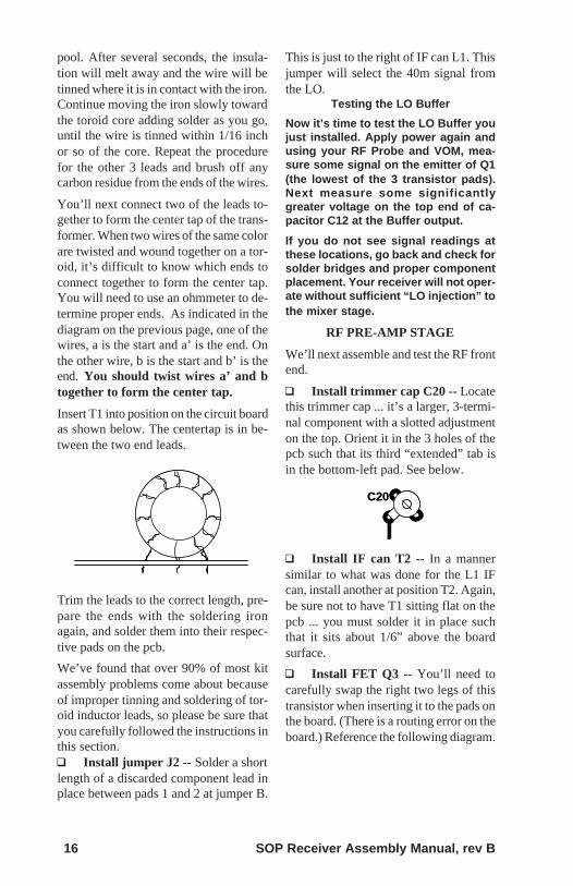
q Winding and installing T1 -- Thisis a fun part of the project that somehomebrewers worry about. There’s actu-ally nothing very hard in winding a fewturns of wire through the toroid core, andwe’ll take you through it in a step-by-stepmanner.
T1 is a “bifilar-wound” inductor on a tor-oid core, meaning that you’ll be combin-ing two magnet wires together and wind-ing them at the same time. Measure offtwo 7-inch pieces of red magnet wire.These wires should be twisted togetheras illustrated below.
a
b
a'b'
a
b
a'b'
(Just twist the wires loosely together byhand ... they don’t have to be very tightlywound at all.)
You will then wind the combined, twistedwire pair around a black FT37-43 toroidcore. See the diagram below for properconnection of the four leads:
b a
b' a'
You’ll next need to strip off the redenamel coating from the transformerleads. The heat strippable magnetic wirebeing used requires no scraping to clearthe red insulation off the leads being sol-dered to the PCB pads. Once the wires ofeach inductor are trimmed to the rightlength (approximately 3/8” extendingdown past the bottom of the core), tin theends of the wires by doing the following.
Using a good hot soldering iron, placethe tip under the end of the wire to betinned and add a little solder so that thereis a small pool of molten solder and fluxon top of the iron with the wire in the
16 SOP Receiver Assembly Manual, rev B
pool. After several seconds, the insula-tion will melt away and the wire will betinned where it is in contact with the iron.Continue moving the iron slowly towardthe toroid core adding solder as you go,until the wire is tinned within 1/16 inchor so of the core. Repeat the procedurefor the other 3 leads and brush off anycarbon residue from the ends of the wires.
You’ll next connect two of the leads to-gether to form the center tap of the trans-former. When two wires of the same colorare twisted and wound together on a tor-oid, it’s difficult to know which ends toconnect together to form the center tap.You will need to use an ohmmeter to de-termine proper ends. As indicated in thediagram on the previous page, one of thewires, a is the start and a’ is the end. Onthe other wire, b is the start and b’ is theend. You should twist wires a’ and btogether to form the center tap.
Insert T1 into position on the circuit boardas shown below. The centertap is in be-tween the two end leads.
Trim the leads to the correct length, pre-pare the ends with the soldering ironagain, and solder them into their respec-tive pads on the pcb.
We’ve found that over 90% of most kitassembly problems come about becauseof improper tinning and soldering of tor-oid inductor leads, so please be sure thatyou carefully followed the instructions inthis section.q Install jumper J2 -- Solder a shortlength of a discarded component lead inplace between pads 1 and 2 at jumper B.
This is just to the right of IF can L1. Thisjumper will select the 40m signal fromthe LO.
Testing the LO Buffer
Now it’s time to test the LO Buffer youjust installed. Apply power again andusing your RF Probe and VOM, mea-sure some signal on the emitter of Q1(the lowest of the 3 transistor pads).Next measure some significantlygreater voltage on the top end of ca-pacitor C12 at the Buffer output.
If you do not see signal readings atthese locations, go back and check forsolder bridges and proper componentplacement. Your receiver will not oper-ate without sufficient “LO injection” tothe mixer stage.
RF PRE-AMP STAGE
We’ll next assemble and test the RF frontend.
q Install trimmer cap C20 -- Locatethis trimmer cap ... it’s a larger, 3-termi-nal component with a slotted adjustmenton the top. Orient it in the 3 holes of thepcb such that its third “extended” tab isin the bottom-left pad. See below.
C20C20
q Install IF can T2 -- In a mannersimilar to what was done for the L1 IFcan, install another at position T2. Again,be sure not to have T1 sitting flat on thepcb ... you must solder it in place suchthat it sits about 1/6” above the boardsurface.
q Install FET Q3 -- You’ll need tocarefully swap the right two legs of thistransistor when inserting it to the pads onthe board. (There is a routing error on theboard.) Reference the following diagram.

SOP Receiver Assembly Manual, rev B 17
q Install C15 and R11 -- Locate thesetwo components and install them in po-sition below trimmer cap C20.
q Construct and install T1 -- Okay,it’s time to make yourself another trans-former! This one is also pretty easy todo. Measure off about 20” of red magnetwire and wind 36 turns around the redtoroid core. But at the second turn ex-tend a little extra past the core body andtwist it together to form a tap. Continuewinding the rest of the 36 turns. This willbe the secondary winding of the trans-former. Measure off another length of redmagnet wire, this time only about 3” andput 2 turns around the core overlappingthe lower two windings of the primary,right up to the tap you created.
s
taps ’
p p’
s
taps ’
p p’
Tin the leads as done before and insertonto the board at position T1. The two(short winding) primary ends will go intothe two pads on the left, and the three sec-ondary leads (two ends and the centertapin the middle) will go into the pads onthe right side of the component. Solderall 5 leads in place, ensuring that no enam-eled wire is in the solder junctions.
Testing the RF PRE-AMP
Connect a temporary wire from the out-put of the LO Buffer (top side of C12)to the ANT pad at the input of the RFfront end. This jumper will supply aknown-good frequency that we can useto test the front end.
Apply power to the board and using theRF Probe measure the signal on the T1secondary winding, located at the leftside of R11. While watching the VOMreading, adjust the trimmer cap formaximum readings.
Move the RF Probe over to the second-ary of T3 (can be probed on pad 3 ofU3). Again while watching the VOMreadings, peak the IF can T2 using asmall screwdriver.
If you did not see noticeable signals atthese points, or if the circuits did notpeak as described, go back and checkfor proper components and solderbridges. Be especially careful indouble-checking the construction jobon T1.
Remove the temporary jumper from theLO Buffer.
MIXER STAGE
We’ll next put the mixer chip U3 in posi-tion.
q Install mixer U3 -- This integratedcircuit is a “surface mount chip”, but it’sa rather large one and relatively simpleto put in place. We were going to pro-vide this part pre-soldered on the boardbut found it to be so straightforward thatwe felt most kit builders could easily ac-complish it.
First tin pad 6 of U3 on the board. This isthe top right pad in the array of 6 padsfor U3. By tinning this pad, you are de-positing a small ball of solder to the padthat will be re-heated with the IC in place,thus holding it down while you solder the

18 SOP Receiver Assembly Manual, rev B
other pins.
Next, locate the IC in the black plasticcase with the clear top. Carefully peelback the top cellophane membrane andthe IC will fall out onto the table.
Pick up the IC with your fingers or withyour needle nose pliers and place over thepads on the board with pin 1 in the topleft corner. (Pin 1 is denoted by a smalldot in the tan plastic package.)
Making sure that the pins of the IC areproperly positioned over their respectivepads, carefully touch pad 6 with the tipof the soldering iron and “reflow” thesolder while gently pushing the IC downonto the pad. With only a small amountof luck, the IC will be held firmly in placeby that one pin, with the other 5 pinsclearly oriented over their pads. (If not,reheat pad 6 and adjust the IC to be cor-rectly positioned.)
Go to the each remaining pin and solderit to the pad beneath it. The pins haveabout the standard 0.1” lead separation,so this operation should be a piece ofcake. Carefully inspect the pads for shorts.
There’s nothing to easily test at this point,so we’ll go on to add the audio filter andamplifier stages next.
AUDIO GAIN STAGE
You’ll next assemble the Audio gainstage: Q4. (You’ll actually assemble allfour stages of the audio chain before wetest them.)
q Install resistors R14, R31, R19 --Note that R31 is installed at position R29along the top of the board. (A small typoon the board designator.)q Install capacitors C19, C36, C21,C34 -- Be careful to observe polarity ofthe electrolytic capacitors. The positivepad is indicated with a ‘+’ on the board.Leave the left end of C19 up in the air,unconnected to the left pad. (We’ll use
this as a signal injection point during testin a few moments.)q Install transistor Q4 -- Note thispackage orientation on the Parts Layoutdiagram.
LOW PASS FILTER STAGE
You’ll next assemble the Low Pass Fil-ter stage.
q Install resistors R15, R16, R17,R18, R20, R21 -- Nothing tricky here.
q Install capacitors C22, C23, C24,C25 -- Nothing tricky here either exceptto ensure that you grab the correct capsfor C23 and C25. These are the darkbrown mylar .01uF caps.
q Install integrated circuit U4 -- Thisis pretty straightforward, as long as youensure you get pin 1 in the square pad.Again, you might want to use a socket tohelp with later debug or modifications.
MUTING STAGE
You’ll next assemble the Muting stag:Q5.
q Install resistors R22, R23 -- Noth-ing tricky here.
q Install capacitors C27, C28 --Nothing tricky here either.
q Install diode D2 -- Just be sure toorient this glass-packaged part with itscathode (banded end) into the lower ofthe two pads.
q Install FET Q5 -- Here again you’llneed to carefully swap a couple of thelegs (this time the left two) of this tran-sistor when inserting it to the pads on theboard. (There is a routing error on theboard.) Reference the following diagram:

SOP Receiver Assembly Manual, rev B 19
q Install pot R24 -- Here’s the firstinstance that you’ll have to install an off-board component. Make sure that youselect the right pot (i.e., the one with theextra two tabs on it) and wire it as shownin the Parts Layout diagram.You’ll now install the final stage of thereceiver: the Audio Amp.
q Install resistors R13, R25, R26,R27, R28 -- Nothing tricky here.
q Install capacitors C29, C30, C31,C32, C33 -- Nothing tricky here eitherexcept to ensure that you are careful toinstall the electrolytics with the properpolarity/orientation.
q Install integrated circuit U5 -- Thisis pretty straightforward, as long as youensure you get pin 1 in the square pad.Again, you might want to use a socket tohelp with later debug or modifications.
OTHER OFF_BOARD PARTS
For the final installation of parts, you’llneed to connect up the remaining off-board controls and jacks. This will en-able you to fully test, and then later oper-ate the receiver. Refer to the Parts Lay-out diagram in the center of this manualfor graphic detail.
q Connect J3 to PHONES-- Usingyour selected hookup wire or cables, wirethe 3.5mm audio output jack to thePHONES pads.
q Connect J1 to KEY-- Using yourselected hookup wire or cables, wire theRCA phono jack to the keyline input atpads KEY.
q Connect J4 to +V-- Using your se-lected hookup wire or cables, wire the
coaxial dc power jack to the +V and GNDpads.
q Connect R9 to TUNE-- Using yourselected hookup wire or cables, wire theremaining pot to the tuning pads TUNE.
q Connect J2 to ANT-- Using yourselected hookup wire or cables, wire theRCA phono jack to the antenna input atpads ANT.
Testing and Troubleshooting theAudio Chain
The figure on the next page repre-sents a higher-level view of theSOP audio section. Debugging pro-cess starts at its output then pro-ceeds backward toward the input.Going at it this way lets you hearwhat’s going. In the interest ofbrevity (and saving trees) we’llshow the debug steps and resultsin summary form.
1) Connect power - no smoke! Usea 9 volt alkaline battery to minimizedamage if something was not rightin the circuit.
2) Check pin 6 of U5- should beabout 1/2 supply voltage.
3) Using an audio signal source(like the one in Section 5), apply au-dio to top of volume control. Atone should be audible in thespeaker or headphones.
4) Apply audio to input of the muteswitch. You should hear a weaktone.
5) Check the dc bias on the outputof low pass filter (U4 pin 7). Shouldbe 1/2 supply voltage.
6) Check bias divider on the lowpass filter input. Should be 1/2supply voltage.
7) Apply the audio source to theinput of the low pass filter (junc-

20 SOP Receiver Assembly Manual, rev B
tion of R15 and R16). Should heartone in loudspeaker and volumecontrol should work normally.
8) Ground the KEY input pad witha clip lead. The tone should disap-pear.
LM386 AUDIO
AMP 2N5485 MUTE
+9V
AUDIO
MUTE
LOW PASS
9) Connect the audio signal sourceto the input of the entire audiochain (i.e., at the lifted end of C19in the Audio Gain stage). Youshould hear a very loud signal, andit can still be adjusted using theR24 level control.
FINAL ASSEMBLY
The only assembly operation needed atthis point is connection of the Mixer stageoutput to the Audio Gain stage input.
q Connect left side of C19 to its pad
CONNECT AN ANTENNA!When you connect a proper antenna tothe ANT input pads (or the J1 jack), youshould hear a significant amount of ac-tivity as you tune through the SOP’s fre-quency range (depending on the time ofday and band conditions).
WHERE THE HECK ARE YOU?Now would be a good time to find aknown-frequency signal on the band, oruse another, calibrated receiver in orderto determine the specific frequency cov-erage of your SOP Receiver. Finding theband edges and marking your front panel
THE SOP KIT IS COMPLETE! ... NOW WHAT???
accordingly would be real useful when itcomes time to operate the receiver.
Of course, if you have purchased and in-stalled the AFA option, you’ll hear theexact frequency of operation comepounding out at you in Morse code fromthe on-board frequency counting circuitof the PIC.
PUTTING THE SOP ON 80MPutting the SOP receiver on 80m is rela-tively easy. You’ll need to add a few com-ponents, and change a couple of jumpersettings on the board, but there’s nothing

SOP Receiver Assembly Manual, rev B 21
major. Just follow the notations on theschematic. These minor mods are prima-rily in the Local Oscillator stage and theRF Pre-Amp stage.
GETTING A WIDER SWINGYou’ll notice that the TUNE pot is con-nected to the regulated 6 volt regulator.This was done to provide a nice, clean,stable signal for the voltage presented tothe varicap tuning element. Without suchregulation, the set frequency would driftwhen the power source (e.g., battery)drooped, dipped, glitched, sagged or oth-erwise varied due to being weak.
If one were to instead provide the higher+V unregulated voltage to the top of theTUNE pot (and its padding resistors),while at the same time provide a stable+V source, a wider swing in frequencieswould be achievable.
Like we said up front, the SOP Receiveris an ideal experimenter’s platform!
FUTURE MODIFICATIONSThere are many mods coming down thepike for this project.
- taking the SOP to other HF bands
- improving the gain and sensitivity
- using alternate designs for some stages
- provide multi-band operation with“daughter boards”
- providing a wider range in the LO
- etc.
There will be some “application notes”published and distributed to the SOPowners, allowing you to have somegreater visibility into the fun times ahead.Lots of plans!
IF YOU HAVE PROBLEMS ...That is, if you have problems in gettingyour SOP to operate, feel free to contactus by email or US Mail and we’ll do whatwe can to help.
For a nominal, flat fee, we will provide arepair service that will guarantee you get-ting back a working SOP (as long as therewas no major component or pcb damage).Contact us for details on this last resortoption.
THANK YOU!Thanks a whole bunch for buying theSOP Receiver Kit and experiencing thefun of homebrewing your own rig withus. The NJQRP Club put in a tremendousnumber of hours designing and puttingthis kitting project together for QRPersall over the world, and we sure hope youare pleased with the experience.
As we stated up front, the SOP is anexperimenter’s platform for learningabout basic receiver operation, straight-forward homebrew kit building, andwhen all complete it’s a flexible little re-ceiver for portable use. And if you’vecome this far in the manual, you surelyhave gained a whole lot of this good ex-perience along the way!
72/73,
--George Heron, N2APB [email protected]
and
-- Joe Everhart, N2CX [email protected]
And be sure to visit the SOP Receiverweb page at the NJQRP Club website:
http://www.njqrp.org/sop

22 SOP Receiver Assembly Manual, rev B
Audio FrequencyAnnunciator (�AFA�)
OptionAssembly Manual
We were able to design in a great feature, in cooperation with DaveBenson, NN1G, to provide the Small Wonder Labs “Freq-Mite” audiofrequency annunciator PIC chip and associated components as anoptionally-purchased add-on to the SOP Receiver. This option pro-vides an incredibly useful feature of an “audio frequency dial” that de-livers the operating frequency of the receiver in Morse code throughthe audio chain of the receiver. With this option installed on the basePC board, the operator merely presses a front panel “spot” button tohear the operating frequency delivered in Morse code through the head-phones or speaker. It’s always accurate and there’s no front panelspace necessary to know where you are in the band. NN1G was verypleased to be able to contribute his Freq-Mite functionality at a veryattractive price to those purchasing SOP kits.
Section 2:
Circuit DescriptionThis circuit from Small Wonder Labs isreally quite simple, yet clever. Referringto the schematic in Figure 2, a PIC16C621microcontroller is programmed as a fre-quency counter.
Transistor Q6 buffers, amplifies and con-ditions the signal coming from the LocalOscillator and presents it to an input portof the PIC. The PIC then counts the num-ber of low-to-high transitions of the sig-nal during a specified period of time, andvoila, the frequency is known.
But wait, that’s only half the beauty ofthis circuit. The other purpose of the PICis to output the computed frequency inMorse code!
When commanded by the operator press-
ing the SPOT pushbutton, an output bitis wiggled at approximately 600 Hertz,and then modulated on-and-off to sendthe Morse code equivalent of the mea-sured frequency through capacitor C43and on into the audio amplifier.
Resistor R43 is used to reduce the ampli-tude somewhat so the Morse frequencydoesn’t wake the next door neighbors.(This is a high-value resistor, and youmay need to adjust it up or down to suiteyour particular needs. Just substitute ahigher or lower valued resistor if desired.)
Because this high-speed digital circuit issitting pretty close to low-level RF cir-cuitry, we took some special precautionsto reduce electrical noise and cross-cou-pling.

SOP Receiver Assembly Manual, rev B 23
The circuit is operated at the lower endof its voltage range, as determined by the4.3 volt zener diode. This lower operat-ing voltage produces significantly lessenergy in its digital waveforms and thusminimizes interferences to the receiver.
The PIC circuitry is tucked into a cornerof the pcb where its effect would be leastnoticeable and where cross-couplingwould be minimized.
And finally, the ground plane for this cir-cuit on the bottom of the board is iso-lated, except for one joining point, thuspreventing digital return paths from flow-ing past or through the RF or audio cir-cuits.
In earlier prototypes of the SOP, we hadwide ground traces on top the board de-
fining the perimeter of the microcontrollercircuit, allowing for a small pcb-cage tobe soldered in place to further isolate digi-tal RF coupling. But we found that thisprecaution was unnecessary and it wasnot included in rev B of the pcb.
For those who have previously used theSmall Wonder Labs’ FreqMite, you’llknow that an “offset” can be set into thePIC’s computation, thus yielding an adderto the base frequency being measured.This allows the FreqMite to be used tomeasure signals in multi-mixing stagesuperhet designs where the VFO fre-quency is not the actual “displayed” fre-quency. But here in the direct-conversionSOP, the Local Oscillator signal is theoperating frequency and the PIC is con-figured through pins 1, 2, 17, 13, 12 11
l
C42.01
6
LocalOsc
D34.3V
U6PIC
16C621
R40470
l
1,2,17,13,12,11,7
5
1516
C4022
C4122
Q62N4401
318
C430.1
14R411.5K
R42100K
C44.0022
LM386AudioInput
+V
SPOTPushbutton
Y 24.096 MHz
RB0/INT
RA4MCLR Vdd
4
RA1
R433.9M
Value to suite desired output lev el: 2.7M-to-3.9M
Vss
RAn,RBn
Osc1 Osc2
l
C42.01
6
LocalOsc
D34.3V
U6PIC
16C621
R40470
l
1,2,17,13,12,11,7
5
1516
C4022
C4122
Q62N4401
318
C430.1
14R411.5K
R42100K
C44.0022
LM386AudioInput
+V
SPOTPushbutton
Y 24.096 MHz
RB0/INT
RA4MCLR Vdd
4
RA1
R433.9M
Value to suite desired output lev el: 2.7M-to-3.9M
Vss
RAn,RBn
Osc1 Osc2
AFA SCHEMATIC

24 SOP Receiver Assembly Manual, rev B
and 7 to provide a Morse readout of theactual frequency being measured. Thus,when the LO is tuned to 7.040 MHz, theAFA will output “7040” to the phones/speaker in Morse code when the SPOTpushbutton is depressed.
PARTS INVENTORYOnce again, the first thing to do is to checkthe contents of the separate bag contain-ing the AFA parts. (This bag has a labelin it indicating that it’s the AFA partsbag.) This accessory only contains theparts required for the AFA feature, andthe components will be placed on themain SOP pcb.
q Install PIC uC U6 -- Locate theintegrated circuit in the black antistaticpad and insert it in the holes for U6 onthe pcb. Be very careful to ensure thatpin 1 of the IC (at the left side of the endwith a detent in the plastic body) goes intothe square pad. (The rest of the pads ofthe IC are round.) It would be a good thingto solder in an 18-pin socket first, insteadof soldering the IC directly in place. Thiswould allow you to remove/replace/re-usethe PIC in other design should you needto later on.
q Install crystal Y2 -- Locate the low-profile 4.096 MHz crystal and put it in
Designator QTY Value DESCRIPTIONC40,41 2 22pF 220J
C42 1 0.01 brow n, 103C43 1 0.1 brow n, 104C44 1 0.0022 222D4 1 4.3V zener diode glass, band at cathodeQ6 1 2N4401 3-pin TO92 caseR40 1 470 yellow -violet-brow nR41 1 1.5K red-green-redR42 1 100K brow n-black-yellowR43 1 3.9M orange-w hite-greenU6 1 PIC 18-pin DIP ICY2 1 4.096 MHz crystal 2-w ire metal case
AFA PARTS LIST
place in the pcb at Y2. Do not have it sit-ting flat on the pcb surface ... you shouldsolder it in place such that it is raised about1/6” above the board, ensuring that itsmetal case is not touching the traces be-neath it.
q Install zener diode D3 -- Locatethis glass diode and insert it in an uprightposition (like you do for the resistors) atposition D3. Be sure to orient the diodesuch that the cathode (i.e., the banded end)is the end connecting to R4. It would bebest to have this cathode end be the onesticking up with its lead folded over. Thisway you’ll more easily be able to probethe circuit later for proper voltages.
q Install C43 and R43 -- You’ll beputting these two components into “thesame” location on the pcb. The left leg ofC43 will be inserted in position just be-low Q6, and its other leg will be pointingstraight up. Thus the component will beleaning to the left. R43 should be insertedto the right hole of C43 on the pcb, andthe other end which is also stickingstraight up should be soldered to the up-pointed leg of C43. Thus, these two com-ponents will be in series. See the figureon the next page for reference.

SOP Receiver Assembly Manual, rev B 25
R43
C43
R43
C43
R43
C43
q Install remaining components:C40, C41, C42, C44, R40, R41, R42,and Q6.
q Clip leads & inspects for solderbridges -- As always, trim all leads downafter soldering and carefully inspect thebottom side of the board for solderbridges.
q Install Jumper A-A -- The lastthing you’ll need to do is to install ajumper wire from pad ‘A’ at the middle-top of the board (just above U3) to theother pad ‘A’ just above pin 1 on U6. Forneatness, you could install this jumper onthe bottom side of the board - it doesn’tmatter. This jumper brings the LO signaldown to the PIC.
OPERATIONUpon power-up, the PIC sends an ‘S ?’ ifyou press the SPOT pushbutton switchwithin about two seconds, the chipswitches to a higher speed (26 WPM)readout rate. It acknowledges this entrywith an ‘R’. If you do nothing the chipmaintains its default 13 WPM readoutspeed.
THANKSMany thanks are due to Dave Benson,NN1G and Small Wonder Labs for al-lowing use of his FreqMite circuit, forproviding us the pre-programmed PICmicrocontrollers at an attractive discount,and for advising us on implementation ofthe design into the SOP Receiver. Daveis an active contributor to NJQRP designand project teams.

26 SOP Receiver Assembly Manual, rev B
The SOP Enclosure is a homebrew one- one that you will assemble from its mostbasic pieces. Don’t worry though, youwon’t have to go through the hassles ofscribing, bending and cutting metal;we’ve already done all that work for you!
This do-it-yourself case is a little differ-ent than most that you may be familiarwith. It is not made of aluminum or steelor even plastic. It’s fabricated from cop-per-clad glass-epoxy printed circuit boardmaterial. Being homebrew, it is a fittingcompanion to the SOP Receiver kit andadds to the enjoyment of your project. Allyou need to do is carefully follow the di-rections in this manual and you will find
it easy to make a very attractive case. Nodrilling, sawing or punching is necessary;only a little soldering is needed, and per-haps some touchup with a file. In fact,once you built it you may even be inspiredto make your own pc board case for thenext homebrew project you have lined up.
Cases made of pc board stock have lotsof advantages over other material. Theraw material is relatively common andeasy to machine. It is lightweight and, insmall cases, quite strong. The copper sur-face provides a good continuous electri-cal shield for electronic circuits insidewhile presenting an outer skin that canbe left “natural” or painted in any color
SOP Enclosure OptionAssembly Manual
This optionally-purchase Enclosure Kit is the ideal homebrew case foryour SOP Receiver. Consisting of 8 precision-cut double-sided cop-per clad boards and assorted hardware, this kit can be assembled in lessthan 30 minutes and can be finished to the builder’s liking or used with its au naturalcopper look.
Section 3:

SOP Receiver Assembly Manual, rev B 27
you want.
If you want a short treatise on this con-struction method check out Joe’s QuickieNo. 34 in the Information Exchange col-umn in the April 2000 issue of the QRPQuarterly.
The SOP Enclosure Kit consists of eightpieces of printed circuit stock which willbe soldered to form the top and bottomof a cabinet. (Skip ahead to Figure 2 tosee a set of diagrams depicting all sup-plied parts.) The case top is an open “U”which sits over another open “U” formedby the case bottom. The bottom also hasinternal side rails which lend strength tothe front and rear panels, and to whichthe top is connected via sheet metalscrews.
Also provided with the kit are the mount-ing hardware, knobs and jacks needed forthe SOP Receiver. Clear acetate sheetoverlays are even supplied to be used asattractive labels for the front and rear pan-els.
PACKAGE CONTENTSIt’s a good idea first off to identify the kitparts and make sure that they are allpresent. The following list details themand identifies the cabinet parts by letter.Match them to Figure 2 on the next pageand check them off in the list as you iden-tify the contents of the parts bags.
Parts list -- Bag 1 a Top cover panel b, cTwo top cover side pieces d Bottom plate e Front panel f Rear panel g, hTwo side rails1 front panel clear acetate label1 rear panel clear acetate label1 right angle alignment gauge
(approx. 1 inch square)
Parts list -- Bag 24 3/8” Nylon standoffs10 #4 x 1/4” sheet metal screws4 Self-adhesive rubber feet
General GuidelinesBefore we start construction, let’s startoff with a couple of tips in case you areassembling a pc board enclosure for thefirst time.
You will need only a couple of small toolsand supplies that are probably already athand. They will be discussed in the textbut here is a sample list:- Soldering iron- Non-acid solder- Scotchbrite or other soap-free non-
abrasive pad- Flat file- Alcohol or other non-water-based sol-
vent- Clear adhesive to attach panel labels- Mechanic’s square (optional)- Rosin core flux (optional)- Paint (optional but an excellent choice
for durability is Rustoleum)- Clear spray (optional though Krylon
clear protects copper from corrosion)
This process has a lot in common withassembly using surface mount compo-nents. While ordinarily solder jointsshould not be relied on for mechanicalstrength, good joints are the only sourceof strength for surface mounting and forpc-board cases. So every effort must bemade to produce good joints.
High quality solder connections beginwith clean surfaces. While the copper-clad board pieces in this kit are shippedin good condition, the copper will forman oxide film over time and normal han-dling can contaminate the surfaces withfinger oils and slight corrosion. A goodpractice to follow is vigorous scrubbingwith a gentle abrasive such as aScotchbrite pad followed by cleaningwith rubbing alcohol or other non-aque-

28 SOP Receiver Assembly Manual, rev B
Figure 2: KIT CONTENTS
5-1/4
5-1/25-1/2 5-1/45-1/4
1-5/161-5/16
Top Half
ab c
5-1/4
5-1/25-1/2 5-1/45-1/4
1-5/161-5/16
Top Half
ab c
5-1/8
1-5/16
5-1/85-1/8
5-1/8
5-1/8
5-1/8
1-5/16
1/21/2
Bottom Half
d
e
h g
f
5-1/8
1-5/16
5-1/85-1/8
5-1/8
5-1/8
5-1/8
1-5/16
1/21/2
Bottom Half
d
e
h g
f
Miscellaneous
TUNESPOTAUDIO
“SOP” 80m/40m CW Receiver
Miscellaneous
TUNESPOTAUDIO
“SOP” 80m/40m CW Receiver

SOP Receiver Assembly Manual, rev B 29
ous solvent. Once cleaned this way thecopper should stay clean enough for sev-eral days so long as you keep it dry anddon’t handle it any more than necessaryduring assembly.
As with any soldering operation, theproper iron and amount of heat shouldbe used. Generally any soldering iron suit-able for electronics use with a 35 to 50watt rating is fine. 600-deg to 800-deg Fshould do the trick if you are using a tem-perature-controlled solder station. Ironswith less wattage will not have enoughheat capacity to produce good joints whilehigher-wattage ones can overheat the ad-hesive that holds the copper onto theprinted board base layer causing delami-nation. A flat chisel tip is preferred overa cylindrical or conical one so that enoughheat can be transferred to the solder as arunning seam is made.
A good quality rosin core solder is finethough some of the more modern “no-wash” type mixes are good too. Do notuse acid core solder as it will destroy yoursoldering iron tip and eventually lead tosevere corrosion of the copper surface ofthe enclosure you are building.
Since you want the top and bottom of yourenclosure to fit snugly without unsightlygaps or seams, alignment of the pieceswhile you are soldering is quite impor-tant. Copper clad board boxes have theirindividual sides joined together at rightangles. Accuracy in aligning each pieceaccurately is what makes the enclosurego together properly and look attractive.
A simple alignment gauge is includedwith the enclosure kit to help you makegood right-angle joints. It is accuratelycut on at least one corner for perpendicu-larity (love those big words!). It is a goodidea to check all four corners against amachinists or carpenter’s square to seewhich one is best. You may also care touse a file to “knock off” 1/8 or so on the
exact corner so that it will fit flush againsta corner of your box after soldering toensure “squareness” in the finished prod-uct. This will also let you know at asglance which is the best corner! Usingthe gauge will be described in the detailedassembly steps so that the enclosurepieces can easily be aligned the correctway.
Finally, you need a good clean unclut-tered work surface! That should be ob-vious, but it is important. When workingwith the pc board material, a fairly be-nign surface is necessary to keep the cop-per on the pc board material clean andscratch-free. A soft cloth or towel laid outon the table surface is best but in a pinchyou can use cardboard or newspaper. Aside benefit of using an overlay on youwork bench is that you will help protectthat surface as well as that of the projectyou are working on. Eliminating clutterhelps you keep track of all the parts.
DETAILED DIRECTIONSOk, the preliminaries are out of the wayso let’s get started! Heat up your iron kickthe kids and pets out of your workshopand turn on your rig so that you can besoothed by the sound of cw on 7040 asyou work.
If you have already inventoried the parts,great! If not please go back to the Pack-age Contents section on page 3 and doso. Select pieces a, b and c to build thecase top first.
Please refer to “Figure 3: Top Half As-sembly” drawing on the next page. Notefrom the end view that the two side piecesb and c will be assembled to the inside oftop cover panel a rather than alongsideit. If the sides are soldered alongside thecover, the cover will not fit on the bot-tom properly. Also observe that the topcover is longer than it is wide so that thelonger side of pieces b and c will beagainst the long dimension of a. Be aware

30 SOP Receiver Assembly Manual, rev B
Insideview
SideView
Endview
o
Case screw hole(1/8”)
a
b cc
acb
Insideview
SideView
Endview
o
Case screw hole(1/8”)
a
b cc
acb
Figure 3: Top Half Assembly
FIG 5: Completed Top Half

SOP Receiver Assembly Manual, rev B 31
that the side view is shown upside-down.When the case is finally assembled the“overhang” will be at the top of the en-closure front panel. All right, that’senough visualization.
Lay piece a on the workbench and set oneof the side pieces (either one) on top of italong one side. Line the side piece upflush with the edge of the top cover, us-ing the alignment gauge to ensure that thetwo pieces are lined up at right angles.The photo in Figure 4 demonstrates howthis is done. [Note: The one photo wehave of using the alignment gauge tech-nique actually shows its use in solderingthe side rails to the base (described inthe next pages); but the technique is thesame as used in soldering the top halfsides.] It may seem awkward at first sinceyou have only two hands but you have todo it with only one hand since you willneed the other for soldering!
Carefully load some solder on your sol-dering iron top and place a solder “tack”
in the middle of the seam between the sideand top pieces to hold it in place. Nowadd a couple more tack joints about ½inch or so from the front and back edgeswhile holding the pieces together with thealignment gauge. When complete, theside and top covers should be accuratelyat right angles. Check along the seamfrom front-to-back and carefully redo thetack joints as needed to get the properalignment.
Once you are sure of correct alignmentyou can complete the solder seam. Youhave two choices here. If you are cau-tious and don’t want extra bother, don’trun the seam all the way out to the frontand rear edges of the cover. That is, keepthem back about 5/16 inch from the frontface of the side pieces and about 1/8 inchfrom the rear face. If you are adventur-ous, run the seam all the way out. Thiswill require a little filing on the bottomcover later, but will give you a somewhatstronger box. To make the continuous
Figure 4: Use of Alignment Gauge

32 SOP Receiver Assembly Manual, rev B
seam, start at the back end of the seamand slowly add solder to the joint as youmove the soldering iron along the seam.Take care not to disturb the right-anglethat the cover and side piece make witheach other.
Now that you are an accomplished ex-pert, repeat the above process with theother side piece. You now have a com-pleted top cover! It should look like thephoto in Figure 5.
Bottom Half AssemblyNext you will assemble the bottom cover.Begin by identifying bottom cover d frontpanel f and rear panel e. You can tell thefront and rear covers apart by noting thatthe front panel has three holes while thereare four on the rear.
Examine Figure 6, the Bottom Half As-sembly drawing, as illustrated on the nextpage. It shows that the front and rear pan-els mount on the outside edges of the bot-tom cover and the side rails go betweenthe end panels inside the whole shebang.
We’ll first solder both side rails (parts g
and h) to the base plate (part d). By plac-ing the smaller, less-critical side rails inplace first, the later step of soldering thefront and rear panels in place will be mademuch easier.
Using the alignment gauge exactly asshown previously in figure 4, solder oneside rail in place using the tack-first,seam-solder second technique already de-scribed. The side rails are identical andcan be used interchangeably. Make surethe edges of the side rail are even withthe front and rear edges of the base plate,as this flush right angle edge will be themounting datum for the front and rearpanels. Don’t worry if the side rail is notexactly even with the base plate, as you’llhave a chance to “square things up” withthe flat file before putting the front/rearpanels in place.
Next, solder the second side rail in placein the same manner as you did for thefirst one. Now is the time to file the edgesto ensure flush perpendicularity.
You next solder the front panel (part f)
d
e
gh
f
e
og
f
ed
Insideview from
top
Right (or left)Side View
Case screw hole(1/16”)
d
e
gh
f
e
og
f
ed
Insideview from
top
Right (or left)Side View
Case screw hole(1/16”)
Figure 6: Bottom Half Assembly

SOP Receiver Assembly Manual, rev B 33
onto the bottom plate (part d). Ensurethat the front panel is aligned square andflush with the base/rail assembly. Hold itin place with the claw grasp of one handas you tack solder several points alongthe joint. Use the same solder-tack tech-nique as you did for the top cover thenrun a continuous joint in the seam afterensuring proper alignment.
Repeat the same process to solder therear panel e to the bottom plate d.
You’re coming along nicely now! Yourcompleted bottom assembly should looksomething like that shown in Figure 7.
It’s a good idea at this point to fit the topcover over the bottom to be sure thateverything fits. It should be a snug fit butnot so tight that you will stress the topcover when it is installed. If you ran thesolder bead all the way out on the topcover you will find that it interferes withthe edges of the front and rear panels.Never fear – we’ll take care of that next.
If you have continuous solder beads outto the front and rear panels on your topcover it is now necessary to perform asmall amount of cosmetic surgery. File
off the sharp corers on the front and rearpanels so to clear the top-cover bead. SeeFigure 8. You only have to “knock off”about 1/16 inch so don’t get carried away!
When you are sure that the covers nesttogether properly, put in the two sheetmetal screws that hold the top and bot-tom halves together. The first time thatyou screw one of the screws into place, itwill be a hard turn on the screwdriver.
Figure 7: Completed Bottom Half
Figure 8:Fitting Top Cover

34 SOP Receiver Assembly Manual, rev B
This is because you are cutting threadsinto the pcb material on the side rails. Butonce you have these threads in place, in-sertion and removal of the screws shouldbe much easier to do.
Do not overtighten these screws! If youare careful in tightening they will last formany on and off cycles. If you inadvert-ently strip one out by over-tightening,drill out the top cover screw holes and goto the next larger size sheet metal screw!
The pc board edges and corners of theassembled enclosure are sharp and ratherabrasive. You may care to bevel them toprotect your fingers and keep the boxfrom damaging tabletops and anythingelse it comes in contact with. A coupleof swipes with a flat file will do the trick.Early samples of case like this had a nastytendency to poke holes in bags and knap-sacks before being refined this way!
Figure 9 below is a photo of the bottomof a complete enclosure with the sidescrews in place. Note the flush and evennature of all pc board edges.
FINIS HINGAt this point you have a completed en-closure! All that remains is to do somefinal finishing as you see fit and to installthe SOP Receiver and associated hard-ware.
Painting is a personal thing. While somecare to leave a “natural” copper finish,others want to personalize their projectsby painting them outrageous colors ormatch them to other equipment they mayhave. The whole process is beyond thescope of this manual but here are a coupleof tips.
1) If you are going to paint your enclo-sure be sure that all soldering is finished.The heat from soldering inside the casewill conduct through the wall and dam-age your nicely painted surface.
2) Surface preparation is very importantto ensure that the paint adheres properly.Use a Scotchbrite pad to remove surfaceroughness and clean the metal immedi-ately prior to painting with acetone, work-ing in a well-ventilated area so that youdon’t suffer respiratory distress.
Figure 9: Completed Enclosure -Bottom View

SOP Receiver Assembly Manual, rev B 35
3) For a well-preserved “natural” copperfinish that will not tarnish use a clearacrylic spray such as Krylon ™ clearspray.
4) Other spray-on acrylic colors will workokay for the short-term but may have atendency to chip or get scratched in time.An oil-based paint like Rustoleum ad-heres well and gives a tough finish.
5) Chose a light color if you are going touse the acetate overlays provided with thekit. The lettering on them is black, butmay not have much contrast against adark surface.
FRONT & REAR PANEL LABELSAcetate labels are provided in your En-closure Kit to help you create a neat andprofessional-looking project case. Theseclear overlays are pre-printed but do nothave holes cut in them for panel-mountedcontrols and connectors. Once in placeon the panels, a sharp hobby knife suchas an Xacto knife will cut holes in theappropriate control/jack locations quitenicely. A good treatise on labels is“Homebrew Chassis and Panel Labels”by Ed Roswell, K2MGM. It appeared inthe Winter 2000 issue of the QRPHomebrewer.
If you choose to use the acetate labelsprovided in this kit, merely cut each oneout carefully along the outside of the rect-angle defining the panel perimeter. Thiswill allow the rectangle to be present onthe panel when complete.
Next, spray adhesive or apply a light coat-ing of rubber cement on the panel andcarefully position the acetate label sheetover the panel and press into place. In afew minutes, the adhesive will be dry andyou can delicately cut out the holes in theacetate over the control/jack holes of thepanel. (Trick: Let the panels dry thor-oughly, or even wait overnight, and theholes will be easier to cut.)
It’s a good practice to lightly spray thefront of the acetate label with clear acryliclike Krylon. This will protect the blacktoner (comprising the actual labels) frominadvertent scraping.
See Figure 10 above showing the rearpanel with labels applied. The front panellabels are shown in the photo on the coverof this manual.
See Figure 14 at the end of this sectionfor actual-size graphics used to create theacetate labels. If you need to make an-
Figure 10: Rear Panel with Labels

36 SOP Receiver Assembly Manual, rev B
other set of labels, you can run that pagethrough a copier using transparency ma-terial instead of paper in the copier.
FINAL STEPSAll that needs to be done now is the fin-ishing touches.
Rubber Feet - Carefully peel off theblack rubber feet supplied in the strip andapply one each to the bottom side of theenclosure. Make sure they are alignedorthogonal and uniformly for maximumesthetics. (That is, put them neatly inplace!) If the surface of the pc board ma-terial is clean, the rubber feet should stayin place for a long while.
Put the top half of the enclosure on thebottom half and secure it using the twopreviously-used screws.
INSTALLING THE SOP BOARDNow that your enclosure is all assembled,painted and labeled, all that needs to bedone is to install the SOP circuit boardand control hardware.
The SOP Receiver board will be sup-ported by four nylon standoffs, securedby small #4 sheet metal screws.
Using small sheet metal screw (supplied),
attach a nylon spacer to the bottom sideof the board at each of the four holes onthe SOP board. The screw will be insertedfrom the top side and protrude down andinto the nylon spacer on the bottom ofthe board. You’ll be cutting threads intothe spacer, and it will be a tight turn ofthe screwdriver. Hold the spacer tightlywith your pliers and turn the each screwdown into its respective spacer until theboard is tightly contained between thescrew and spacer on each end of theboard’s rear edge.
Next, carefully insert the board assem-bly into the enclosure and position it overthe four holes in the base plate. Using thesame technique as above, screw four #4sheet metals screws (supplied) throughthe bottom of the case and up into thefour nylon standoffs on the board. If theholes do not perfectly line up, try loosen-ing the top side screws and let the nylonwasher float into the correct positionwhen screwing the bottom screw in place.Worst-case, if the holes cannot be madeto line up, just use 2 or 3 screws on thebottom, and the board will still be heldsecurely in place.

SOP Receiver Assembly Manual, rev B 37
QUESTIONSThis method of homebrewing project en-closures is bound to be growing in thefuture. Opportunities for modificationsand personal customizations are limitedonly by your imagination. One of ourmembers of the NJQRP Club has a projectin progress wherein he is making the en-closure for his 2N2/40 Transceiver com-pletely out of pc board material, just likewith this basic SOP design. In addition,
he’s also fabricating an entire, modular,multi-board inner structure out of the cop-per clad boards. Homebrewing bound-aries have officially been extended to thehorizon!
If you have any questions or problemswith the enclosure aspects of this project,please feel free to contact us by email orby US ground mail. We’ll do our best tohelp you fully enjoy all aspects of yourhomebrew enclosure.
AU
DIO
SP
OT
TU
NE
“SO
P”
80m
/40m
CW
Re
ceiv
er
AU
DIO
SP
OT
TU
NE
“SO
P”
80m
/40m
CW
Re
ceiv
er
PO
WE
RA
UD
IOA
NT
EN
NA
KE
YLI
NE
PO
WE
RA
UD
IOA
NT
EN
NA
KE
YLI
NE

38 SOP Receiver Assembly Manual, rev B
A view of the Rear Panel Jacks
A View of the Front Panel Controls

SOP Receiver Assembly Manual, rev B 39
SOP Controls OptionAssembly Manual
This optionally-purchased Controls & Hardware Kit is another “idealcompanion” to the basic SOP Receiver. All of the front panel controlsand rear panel jacks are provided to enable the homebrewer to quicklyand easily bring his SOP Receiver to a working state. These controlsmate perfectly with the Enclosure Kit (another optional purchase) toform the completely operational receiver.
Section 4:
This will be an easy accessory kit to dealwith. What you’ll do is wire the controlsand jacks to the board as shown in thefigure on the next page.
Parts InventoryThe first thing to do is to compare thecontents of the little plastic bag contain-ing the controls and jacks to the Parts Listshown on the next page. Make sure ev-erything is present before you begin.
Carefully remove the nuts and washersfrom the two 1/8” jacks, the coaxial DCpower jack, and from the RCA phonojacks. Install each into its respective lo-cation on the front and rear panels of yourfavorite enclosure. If you haven’t yet se-lected or prepared your enclosure, youmay of course just wire these parts di-rectly to the board and leave them hang-ing in “free space” off the end of the con-necting wire
Using short insulated hookup wire, thinRG174 coax cable, shielded audio cable,or whatever other wire you might havehandy in your junk box, connect theground and signal/power wires of eachcomponent to the respective pads alongthe edge of the circuit board.
J3 3.5mm jack -- The ground terminalon this PHONES jack is the little one on
the side, and the signal terminal is thelarger one on the opposite side.
J4 coaxial DC power jack -- The groundterminal is middle one, and the +V ter-minal is the one on the left. (The rightterminal is unused.) Wire the +V termi-nal over to the switch on the Audio po-tentiometer. (See that section below.)Wire the ground terminal directly to thepcb pad for GND, next to the +V pad.
J1, J2 phono jacks -- The ground termi-nal of these is the tabbed washer (bend itslightly up and away from the case in or-der to solder the ground wire to it.) Thesignal wire should be attached to the cen-ter terminal of the phono jack. Wire oneof the phono jacks to the KEYLINE pad,with its corresponding ground wire go-ing to the GND pad next to the KEYLINEpad. Wire the other phone jack to theANT pad on the pcb, with its correspond-ing ground wire (or shield of the thin coaxused) to the GND pad next to the ANTpad.
R24 Audio Potentiometer -- This potalso contains the power switch, so wirethe 2-tabbed side of this control betweenthe power jack and the +V pad of the pcb.Wire the 3-terminal pot tabs to the pcb asshown in the diagram.

40 SOP Receiver Assembly Manual, rev B
R9 Tune Potentiometer -- This pot isjust a pot. Wire its 3-terminal tabs to thepcb as shown in the diagram.
Front Panel Knobs -- Using a small flatblade screw driver, partially unscrew theset screw from each knob until they areable to be slipped onto the shafts of thepotentiometer controls. [The followingapplies if the pots are already mounted ina front panel.] With each pot shaft turnedcompletely counterclockwise, rotate theknob (which is still loose on the shaft)such that its indicator is pointing to theseven o’clock position and tighten the setscrew. This will give the pot and knobnormal relative indications during opera-tion.
CONTROLS & HARDWARE PARTS LIST
PB1 pushbutton -- This little red-toppedpushbutton is used as the SPOT switchfor the Audio Frequency Annunciatoroption. When pressed, it triggers theFreqMite microcontroller to sound thecurrent frequency through the PHONESjack. (We figured that most people wouldbe interested in the AFA option; but evenif not, this pushbutton would nicely fillthe front panel hole!)
Extra Plugs -- In a further attempt to easethe job of getting your SOP Kit opera-tional, we’ve included the mating plugsto some of the jacks on the rear panel.Two phono plugs (P1, P2), and a coax dcpower plug (P4) are included to allow youto wire up the mating cable for the an-tenna, keyline and dc power.
Designator QTY Descr iptionJ1, J2 2 RCA Phono jack, nickel plated, ground, black insulator J4 1 DC pow er jack, 2.1mm, molded, economy, w ith NC sw itch Knobs 2 Black plastic knob w /blue top, .25" shaftP4 1 DC pow er plug, 2.1mm x 5.5mm x 9.5mm black locking, barrelP1, P2 2 RCA phono plug, black plastic insulator, hollow center pinR24 1 Audio pot , 10K-ohm miniature potentiometer w /sw itch R9 1 Tune pot, 50K-ohm miniature potentiometer PB1 1 Pushbutton sw itch, normally open, momentary contactJ3 1 3.5mm jack, black, panel mount
PC BOARD LAYOUT
R24
J3
J1
J4
PB1
R9
J2
PC BOARD LAYOUT
R24
J3
J1
J4
PB1
R9
J2

SOP Receiver Assembly Manual, rev B 41
Test & MeasurementCircuits
Here are two simple circuits that can be effectively used to get yourSOP Receiver into tip-top shape. The first is a great little audio oscil-lator contributed by Joe Everhart, N2CX. With this useful gem you’llbe able to inject low-level signals into your audio chain and trace themthrough to the speaker. The other circuit is a standard-but-nifty RFProbe , contributed by Chuck Adams, K7QO as part of his series ofarticles concerning “Manhattan-style construction techniques”, pub-lished in QRP Homebrewer. With the RF Probe you’ll be able to mea-sure the signal coming from your local oscillator, the LO buffer andother RF signal sources. Very handy indeed!
Section 5:
Twin-Tee Audio Oscillatorby Joe Everhart, N2CX
This circuit is an old favorite of mine. Itwas the very first Joe’s Quickie in theQRP Quarterly’s Information Exchangecolumn and is still a favorite on the N2CXworkbench. Though very simple, this cir-cuit is an excellent signal source for de-bugging and troubleshooting.
Power is supplied by a 9-volt battery (acarbon-zinc “cheapie” is fine) and theoutput is a 1 KHz sine wave. A simpleresistive divider from the transistor col-lector reduces the output to about 1 mVwhile the 0.47 uF capacitor provides DC
isolation. Check the original article for atable of resistor attenuator, which set theoutput levels.
It’s a pretty non-critical circuit that canbe built ugly or beautiful. I built mine ona scrap of perf board. There is no powerswitch; to turn it on I simply clip a 9-volt battery onto the power connector.And there’s no fancy output connector,either. An output and ground lead arewrapped over the edge of the board foraccess to a clip lead or soldered-on wires.
.47
100
100K
4.7.047
22K 22K
22 3.3
.022 .022
+9V
2N2222 500 Hz ~ 1 mV

42 SOP Receiver Assembly Manual, rev B
Building an RF Probeby Chuck Adams, K7QO
The first thing to build is an RF probe.Go to the ARRL Handbook to page 26.9and look at figure 26.9(C) for a voltagedoubler circuit. Don’t use the entire cir-cuit. All you need is C1, C2, D1, and D2.The AC input will be the RF signal andthe point at which D1 and C2 meet willbe the +DC output. Eliminate R1 and R2from the circuit. The values here are nottoo critical and you can experiment withthis. Use something like 0.1uF or smallerfor C1 and something like 0.47uF orlarger for C2. For D1 and D2, use eithergermanium or silicon diodes. I used somesurplus printed circuit board leaded di-odes that I got surplus somewhere and oftype 1N4148 or 1N914 silicon diodes.
I won’t go into the nitty-gritty details here,but you need three pads and just a smallsegment of printed circuit board. Becausethe leads were short I mounted the diodeshorizontally. D1 is between two pads. D2
is soldered to the center pad and the otherlead soldered to the ground plane. Withlonger leads you can mount the diodes ina vertical position. The probe will workthe same with either configuration.
I have a Ballantine RF probe that I pur-chased for $10 at a Livermore Swapmeeton a trip to CA when I was working. Thisprobe came sealed in an aluminum pouchwith all kinds of military part numbers,etc. Probably cost the tax payers a fewhundred dollars. I compared my readingswith the RF probe built Manhattan-styleand the Ballantine probe and got the sameresults to over 40MHz. The one hereprobably cost me about a quarter. Thecommercial probe is nice, but not every-one can find such a great deal. Besides,in the building of homebrew gear you cantake extra pride in using something thatyou personally built and can repair.
Your VOM should be set for DC volts,and your reading will then be RMS volts,or Vrms = Vpeak * 0.707.
VOM
-+To circuit
beingmeasured
VOM
-+VOM
-+To circuit
beingmeasured

SOP Receiver Assembly Manual, rev B 43

44 SOP Receiver Assembly Manual, rev B