solid-state oscilloscope - keith-snook. · pdf filesolid-state oscilloscope ... radio, more...
TRANSCRIPT

110 Wireless World, March 1969
Solid-State Oscilloscope
Circuit details of a test instrument designed for work on colour TV receivers.
by Michael Phillips
To be capable of performing all the measurements needed on a colour television receiver an oscilloscope must be able to provide accurate results from d.c. up to the sub-carrier frequency of about 4.4 MHz. Experiments with a colour decoder confirmed that an elderly, low-frequency oscilloscope did not have sufficient bandwidth for such work and it was decided that the cheapest way of obtaining improved performance was to construct a new vertical amplifier as an add-on unit using the existing tube and e.h.t. supply. This was later extended to include a new timebase, X amplifier and square-wave calibrator.
An important requirement of this type of conversion is that the amplifiers should be designed to supply the high deflection voltages, 250 to 300 V peak-to-peak, needed by older types of oscilloscope tube. This was made easy by the availability of inexpensive silicon transistors intended for use as video amplifiers in television receivers, resulting in simple, low-power circuits giving high output voltages at bandwidths that would be difficult to achieve with valve amplifiers.
Performance figures which follow refer to a 5CP1 tube with a supply of 1.25 kV plus an additional 1.25 kV on the p.d.a. electrode and will be typical for most 13 cm. tubes of this vintage. With more modern, higher
Michael Phillips served in minesweepers during and after the war and then went to college in 1947. For five years, 1950-55, he was engaged on radio and test-gear development with Ultra Radio. He has been with Bush Radio, more recently Rank Bush Murphy, for the last 12 years and is now project leader for monochrome television development.
sensltlvlty tubes these figures can be improved upon since both amplifier gain and output voltage swing requirements are less. Possible modifications to the circuits are described later.
Vertical amplifier
The response of the vertical amplifier is flat from d.c. to 6 MHz and is 3 dB down at I I MHz, the maximum sensitivity being 100 mV per cm. The gain can be switched for a X 10 increase with a reduction in the 3-dB bandwidth to 1.5 MHz. The circuit divides conveniently into two sections. Fig. I shows the pre-amplifier, which includes the input attenuator and all the controls, and Fig. 2 the output amplifier which should be situated as close to the tube base as possible. The input attenuator uses compensated potential divider sections presenting a constant input impedance of I MO in parallel with approximately 20 pF. Attenuator switching sequences tend to be a matter of personal preference so a choice should be made from the values given in Table I. For most purposes ordinary carbon resistors with a tolerance of 10% are
quite satisfactory and are much cheaper than high-stability types.
When using a high-impedance probe any difference in the input capacitance between different attenuator sections must be compensated for by adjustment of the probe trimmer. This can be avoided by connecting trimmer capacitors of about 10 pF maximum from each position of SW2a to earth. A suitable probe consists of a 9. I MO resistor shunted by a 3-12 pF trimmer and mounted in a metal tube (some cigar containers are ideal). The probe should connect to the oscilloscope through about
Table 1
Sensitivity Ra (0) R. (0) Cb (F)
200mV 510 k 510 k 20 p 300 mV 680 k 390 k 39 p 500 mV 820 k 200 k 68 p
1 V 1 M 110 k 180 P 2V 1 M 51 k 400 P 3V 1 M 33 k 500 p 5V 1 M 20 k 1 n
10 V lM 10 k 2n 20 V 1 M 5.1 k 4n 30 V 1 M 3.3 k 6n 50 V 1 M 2k 12 n
Values for the Y input attenuator of Fig. 1. A choice should be made for either 1-2-5 or 1-3-10 range sequences, Ca for each section is a 30 pF max. mica compression trimmer.

Wireless World, March 1969
r------�-- +H.T.
2 2k
Vrl �-_--+-c.: 10k
27k
O.C. A.C. -
Ind 0
o
0'01/L
47p (Ceramic)
150
SWl ..... -.......
0·1/L 400V
.. , .)
a,800p
2·2 k
111 A
r---------1-----------4r------ +12V
820 P
S·2k
Tr2
Tr3
270
Vr2 20k
S·2k
270
Set Iloin Vr3 Vr4
SW3
xl0 xl aop (Ceramic)
Gain 500
+12V
Tra
5·ak
5·ak
Output 1
Supply decoupling 10
A "'1If;--"11---4I�vvvo.-- +12V
�eT �'1
/LT
2OJJ fI.1 From
power supply
B �6vI 0'1
/L 1 ...... f-... -----........ '\fV\,/\,-- -12V 10
Output 2
B � ____ -4 __________ ��---------+-----12V
Fig. I. Circuit diagram of the vertical preamplifier. Resistors are I/4W carbon; capacitors are polyester type 250 V working unless otherwise marked. Preset resistors are 1/4 W carbon.
I metre of screened coaxial cable with a resistive inner conductor (Ref. I). The input impedance increases to 10 MO but with an unavoidable attenuation of 10: I. Impedance matching between the input and the base of the first transistor is provided by a cathode follower valve VI' A valve is used in this position to simplify the problem of allowing direct coupling to the input and to limit the effects of a severe voltage overload on the semiconductor devices in the amplifier. The anode voltage for VI is derived from the h.t. + line via the emitterfollower TrI thus giving low-impedance decoupling down to zero frequency at the anode.
Although it would probably not be as robust a buffer device, an f.e.t. could no doubt be used to replace the valve cathodefollower if one wanted completely solidstate equipment. A commonly used circuit is the source-follower with the source supply voltage and/or the source load resistor adjusted for zero drift operation. Some useful information on the subject is included in Ref. 2. The valve is followed by a long-tailed pair phase-splitting amplifier, Tr2 and Trs. Constant current transistors, Tr 3 and Tr 4> are used in the common emitter impedance to reduce the gain loss which occurs with resistors. Gain control is effected by selection of the resistors bridging the two emitter loads and pre-set resistors are switched for the x I and x 10 gain ranges with a common variable control in series for front panel adjustment of calibration.
The vertical shift control adjusts the d.c.
voltage on the base of Tr5; this ensures that the amplifier stages are operated in a balanced condition when the trace is along the centre line of the tube face whatever the d.c. level is at the input. Capacitance loading across the 6·8 ill collector resistors is reduced to a low value by using emitter-
4'7k
3W
Y-platel
+H.T.
SOp
followers Tr8 and Tr7' for coupling to the output stage and in practice the -3 dB response point due to the collector components is at about 30 MHz. Compensation for the fall-off in amplifier gain with frequency is provided by the 60 pF capacitor across the gain control resistors.
2'5 x 5cm copper (or phosphor bronze)
-12V from Amplifier 10 power supply
�
1
4'7k 3W
Y- plate 2
10k To
trigger unit Fig. 2. Circuit diagram of vertical deflection
amplifier and (right) an example of a heat sink required for Trs and Trll'

112 Wireless World, March 1969
�---1------�-----1-----1----�r---------------1r-----,------�--------- +15V
I Jji SW4a Trigger : -from --i
Y-amplifier 0'1!' :
39k 4·7k 39k
5'6k 560
L ___________ � _____________ __ _ _ _ ____________ I
Trigger input D1
•
1 k
Amplitude 10k
1aOk
4'7k
1 k
Gate pulse outpu.
1!'1I 100msec
0 10msec 0
o-II0'1/L 1msec 0
o 0,01!'1I 0 sW5b sW5a 0---1 I l,OOOp 100!,sec
0
« 1O!,sec
« J( Cc 150p 1!,sec
Stobil ity
Yr7 /� Yra L-_'1'-_--''1'-_...J�--5...,k �/ r 500 Cal-
Free I run + 470
470
1 k
2'2M
56k
External input
2·2k
+15V
1 0.1!'
Ext.
Int.
3'3k Vr 11
5k
47k
47k
10p 47k
X-shift circuit con be remote trom
X-output ampl ifier
Fig. 3. Circuit diagram oJ time-base trigger unit.
,,--"---�---+H.T.
33k X-shift 1W
3'3k
3'3k
4'7k 3W X- plate
_oN'V'VV'_ -12V
470
-------- ----+-c X-plate
-5V '----.... +H.T.
Fig. 4. Circuit diagram oJ ramp generator and horizontal output amplifier. Diodes are general purpose germanium types such as the DABr.
Output from the pre-amplifier is at low impedance and open wire leads of 20 cm or more in length can be used to feed the output amplifier. This again uses the longtailed pair configuration with transistQrs as the common impedance. The circuit is shown in Fig. 2. With a total capacitance load due to the tube plates and the transistors of about IS pF per collector, frequency compensation is necessary and is provided by the 80 pF capacitor linking the two emitters and by inductance in each collector load circuit. The coils need about 60 turns of 32 s.w.g. enamelled wire wound as a single layer on a former with a 4 mm core.
Turning now to the active devices used. VI is a small, low-consumption triode or strapped pentode such as the EF9S/6AKS. The small size of Nuvistors makes them ideal and they are frequently used in commercial instruments. Transistors in the pre-amplifier are low-power silicon devices
typified by the BCI07 with an h" of 12S-Soo and anJT of about 8S MHz. The output amplifier uses high voltage transistors, suitable types being the BFI78 and the older BFI09 from Mullard or the SGS-Fairchild BFIS7. Small clip-on heat sinks will be required and a 2.S X S cm strip of thinnish copper or phosphor bronze formed to wrap round the transistor as shown in Fig. 2 will be satisfactory. A smear of silicone grease between transistor and sink assists heat conduction. Remember that the collectors are connected internally to the TOS case, so the heat sinks will be "live". A similar transistor can be used for Trl which operates with a Vce of about 60 V, a small heat sink again being required.
The output amplifier works with an h.t. of 120 to ISO V depending on the rating of the transistors and the output drive required. Current drain including the cathodefollower is about 30 mA.
Horizontal deflection
The horizontal deflection section consists of a trigger unit, a calibrated time-base and an X amplifier which includes an optional pre-amplifier for external signals. A circuit diagram of the trigger unit is shown in Fig. 3. An emitter-follower Tr12 takes its input from either the Y amplifier or an external source and is followed by a phasesplitting amplifier Tr13 and Trw for polarity selection. Two transistors, Tr15 and Trl8> form a Schmitt trigger circuit and the differentiated output from this is used to trigger the time-base.
The time-base and amplifier, which is shown in Fig. 4, uses the emitter-coupled circuit described by Gilbert in Refs. 3 and 4 where a full account of the operation is given together with a most impressive list of advantages. Transistors Tr17 and Tr19 are coupled by the emitter-follower Tr18 and by

Wireless World, March 1969
the charging capacitors. A positive-pulse through the trigger hold-off diode initiates the action, resulting in a negative-going linear ramp in the emitter circuit of Tr19• Tr 20 forms a source of constant charging current. There is a small step at the start of the ramp which shows up as a bright spot at the start of the trace. This can either be cancelled by the various means described in the references or minimised by using the negative-going square pulse at the emitter of Tr18 as a bright-up pulse on the c.r.t. Three preset resistors in the emitter of
Trzo are switched to provide a x I, X 2 or x 5 multiplier for the decade capacitors selected by SWs. Adjustment of Vrg gives a variable interpolation. The total range is from 500 ms to I Its per sweep.
An emitter-follower Tr21 couples the sweep to the main X amplifier which uses the same long-tail pair circuit as is used in the Y amplifier. The input is single-ended so shift voltages are applied to the other amplifier base. Frequency compensation is supplied by the capll.citors from the shift control to earth and across the feedback
330 -12V
lOO
33k 33k
Tr28+---HL
1'8k 330 4'7k
113
resistor. This resistor can either be pre-set or, if it is mechanically convenient, brought out as a variable sweep-width control, preferably switched as a sweep multiplier. Transistors used in this section, Tr12 to TrZ5' are of the same types as those in the Y amplifiers except for the Schmitt trigger circuit. Here it is recommended that OC44 or OC45 transistors are used. Although any transistor type can be used in this kind of circuit their behaviour with a large input signal is quite different. With sine-wave input the OC44/45 transistors produce a clean square-wave output with up to 60 V peak-to-peak input. Above this the tips of the sine-wave break through symmetrically. Experiments with the BCI13 silicon planar and the BCI07 planar epitaxial transistors show unsymmetrical break-through with a much lower input of about 12 V peak-topeak. Alloy diffused transistors of the AFII4-II5-II6 family are the worst tried, with break-through at about 4V input. These remarks apply to both the trigger unit and to the Schmitt trigger squaring circuit in the calibrator.
Fig. 5. Circuit diagram of optional X pre-amplifier.
For the display of external signals, such as a wobbulator time-base, the sensitivity at the base of TrZl will generally be sufficient. If extra gain is required, the a.c.-coupled circuit shown in Fig. 5 is suggested. This provides a sensitivity of about 100 m V/cm at a bandwidth of 5 MHz. The input attenua-
r-------�--.---�-�-----�--��-�----- -12V
Vr14 10k
820 820 820
laM
Mark/Space ratio
33k
3' 3k
\ Set frequency
Tr30 OC44 OC45
lExt. SW8
r O'1M
Input
Fig. 6. Circuit diagram of square-wave generator.
2 ·2M 22k
40p
4'7k
2'2k Cd 3-30p
47k
Tr32 OC44 OC45
22k 47k
2'2k 2'2M
0 '1M
Tr33 OC44 OC45
22p
Fig. 7. Circuit diagram of the h.t. + line stabilizer (a) and power supplies for the low potential lines (b).
+12V +1 5V (9mA) (12mA)
2·2 Smoothed h.t. input
(say 250-300V) Tr35
1 '2k Tr36
470
Vr17 Vr18 2.500p
47 47 lOOk 2k 30V 2k
2·2k 2'7k Vr21 lOOk Set +ht.
Vr19 2,500M
220k 2k 30 V
Tr37 Tr38 3'3k 470
2'2
(a) -5V -12V Cb) (6mA) (90mA)
0'1p .-0
Output
Level
18-20V r.m,s.
[;0' 6'3:, V2�
6'35]
114
tor is similar to the one used in the Y preamplifier and is followed by the Darlington pair Tr26 and Trm giving a stage gain of unity but an input impedance of several megohms. The amplifier which follows uses two transistors Tr28 and Tr29 as a common-emitterjemitter-follower pair. This last circuit, incidentally, is quite a useful one in its own right; it has a gain of ten and, with v.h.f. transistors such as those used in TV tuners and with a suitable peaking capacitor across the first emitter resistor, will maintain that gain to over 200 MHz.
For the X pre-amplifier most types of germanium h.f. transistors will be suitable or, with a reversal of all polarities, the silicon devices used in the other circuits.
Square-wave calibrator
This section generates a square wave with an output amplitude variable between 50 m V
and 4 V peak-to-peak from either an internal source at 10 kHz or at any frequency from IS Hz to 20kHz with a sine-wave input from an external a.f. generator. The circuit diagram in Fig. 6 shows a 10 kHz sine-wave oscillator Tr30' an emitter-follower buffer stage Tr3i into which can also be switched the external input, and a Schmitt trigger circuit Tr32 and Tr33 to generate the squarewave. The emitter-follower output Tr34 feeds a simple attenuator which gives two ranges of output amplitude; 50 mV to 400 mV and 500 mV to 4 V. There are preset trimmers for adjusting the frequency and the mark/space ratio, and the trimmer capacitor in the Schmitt trigger circuit is used for setting an exact square-wave. Besides proving very useful for gain calibration, and adjusting the attenuator and probe compensation, the calibrator can also be used as a signal source for square-wave testing.
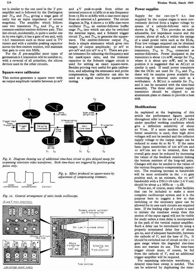
Fig. 8. Diagram showing use of additional time-base circuit to give delayed sweep for examining television video waveforms. Both time-bases are triggered by positive-going pulses only.
JLflfl Under Over
compensated compensated Correct
Fig. 9. Effect produced on square-wave by adjustment of compensating trimmers.
Fig. 10. General arrangement of units inside oscilloscope.
X and Y main amplifiers
Low-voltage power supply
shield
Screeni ng box for
Y-pre-omplifier
Wireless World, March 1969
Power supplies
Supply for the 120-150 V h.t. line required by the output stages is most conveniently derived from a higher voltage by means of a cathode-follower valve as shown in Fig. 7. This provides an easily adjustable, low impedance source and the current, about 58 mA, is within the ratings of a small power valve such as the EL84. Four low voltages required can be obtained from a small transformer and rectifiers via transistors, Tr36 to Tr38, connected as emitter-followers. Power dissipated in the transistors is about lIO mW, except for Tr38 where it is about 900 mW, and in this position it is suggested that an A CI27 or similar is used. If small power transistors like the OC 81 are used for Tr36 and Tr38 there will be surplus power available for connecting to external units such as a wobbulator. A B CI07 is suitable for Tr37 and it can be mounted with the time-base assembly. The three other power supply transistors should be clipped to an aluminium plate or chassis to provide a heat sink.
Modifications
As explained at the beginning of this article the performance figures quoted throughout refer to the use of a 5CPI tube under specified working conditions which give a deflection sensitivity of about 20 V/cm. If a more modern tube with better sensitivity is used, then high drive voltages will not be needed and the collector supply voltage to the output stages can be reduced to some 60 to 80 V. If the same basic input sensitivities of 100 m V/cm and 10 mY/cm are to be retained, then the
overall gain must be reduced by increasing the values of the feedback resistors linking the bottom emitters of the long-tail pairs. Changes will also be needed to the values of
the various frequency-compensating capacitors. The resulting increase in bandwidth will be most noticeable in the x 10 gain position and, as an estimate, the 10 mV bandwidth with a DNI7- 78 tube (7.6 V/cm) should be about 4.5 MHz at -3 dB.
There are, of course, many other facilities that can be included to make a more complete oscilloscope system and it is the purpose here to suggest a few so that switching or the necessary space can be allowed for in case such circuits are required later. If the leading edge of a pulse is used to initiate the time base sweep then this section of the input signal will not be visible for study unless a time delay is incorporated in the path of the vertical output amplifier. Such a delay can be introduced by using a properly terminated delay line of about 400 ns, and of adequate bandwidth, between
the cathode of Vi and the base of Tr2• It should be switched out of circuit on the x 10 gain range where the degraded rise-time does not warrant its use. The time-base trigger circuit must, of course, be fed from the cathode of Vi and an additional trigger amplifier will be required.
For examining television waveforms, a delayed time-base sweep is needed. This can be achieved by duplicating the time-

Wireless World, March 1969
Photograph of the Y preamplifier module.
base circuit and driving it from the trigger unit. The differentiated gate pulse from the new unit is then used to trigger the main time-base. This description will probably be made clearer by referring to the block diagram in Fig. 8.
Setting-up and calibration
To set up the correct d.c. working conditions in the Y amplifier, first adjust for the following voltages: Vr I to give 72 V at VI anode, Vrz for IV at Tra base and Vrs for 8.4 V at the base of Tr.; all voltages positive with respect to the - 12 V line. Vrz is then finally re-adjusted for equal top and bottom limiting on a sine-wave signal of sufficient amplitude to cause overloading. During all these adjustments the Y shift control should be set for zero volts between the bases of Trz and Tr •. Since the amplifier is directly coupled, the preset gain controls Vra and Vr. can be adjusted using a d.c. supply and a voltmeter as the calibration source.
Without access to a good oscilloscope the problem of adjusting the various frequencycompensating trimmers is rather like that of the chicken and the egg. Fortunately however, we can set as a starting point the x I gain 100 mV position on the attenuator. In the absence of any instability the response of the amplifier should be as specified with no irregularities and, since there is no input compensation, this position can be used for displaying the calibrator unit output. Vrl5 should be set for unity mark/space ratio and
. the trimmer in the Schmitt trigger Cd,
to gIve a flat-topped square-wave. The effect on the waveform due to the adjustment of this and the other compensating trimmers is shown in Fig. 9. Once the output from the calibrator unit is satisfactory it can be used for setting the attenuator trimmers (Ca in Fig. I), by adjusting each one in turn to give a flat-topped square-wave display. The 50 Hz mains supply with a period of 20 ms forms a useful standard for setting the timebase range multiplier resistors, Vr9 to Vrll> but for checking the shorter time decades and for setting the I ps trimmer capacitor, a generator covering the appropriate frequencies will be needed.
Construction Since tube sizes and the type and volume of e.h.t. supplies can vary a great deal it is not the intention here to describe the construction in detail. In the title photograph is shown the oscilloscope which has evolved from a series of re-builds as circuit improvements were made, from the original add-on units mentioned in the introduction. It comprises basically a box frame-work made of 1.25 cm angle aluminium. The various circuit sections are built as separate units on s.r.b.p. perforated panels (plain Veroboard) with plug and socket connections to the power supplies. The general disposition of the units is shown in Fig. 10.
The Y preamplifier and the trigger/timebase unit plug-in to the front of the instrument. Construction of the pre-amplifier is illustrated in the photograph above. The att�nuator switch uses three wafers, the resIstors Ra and the trimmers Ca being connected in parallel between the front two wafers, while Rb and Cb connect to the last wafer which is used solely as a common earth. The first panel is used for mounting VI' T.r, and their associated components, the remaInder of the amplifier is wired on the second panel and the supply decoupling components on the rear one. The time-base is quite straightforward except for the choice of a time switch. The alternatives are: an eighteen way switch, separate six and three way switches or, the solution used here, two switches with concentric spindles.
Since the only real sources of heat are the tube and the two valves there are no ventilation problems, two 25 mm holes in the bottom and expanded metal mesh over half the back being all that is necessary.
REFERENCES
1. 'A Wideband .Oscilloscope Probe', by L. Nelson-Jones. WIreless World August 1968, page 275. 2. �escon/66
.Technical Papers. Part 6.
Session 11 on Field Effect Transistors. 3. 'E�itter-Timed Monostable Circuit', by B. Glibert. Mullard Technical Communications July 1961, P. 345.
'
4 .. 'OscilloscDpe Timebase Generator', by B. Glibert. Mullard Technical Communications March 1964, p. 276.
'
The series of articles on the Wireless World Oscilloscope �hi�h appear�d during 1963 and 1964, and which IS now avaliable in a set of five booklets, will be found generally useful for references.
115
Corrections
Some other Measuring Rectifiers
Owing possibly to some clod of earth still adhering to me after resurrection, or to a misguided attempt to be concise, an erroneous statement (in italics, too!) got through in "Some other Measuring Rectifiers" (Feb. issue). While it is true that the bridge rectifier type of voltmeter would correctly read r.m.s. values of square waves if it were calibrated in its natural mean values (because the mean and r .m.s.-and peak -values of square waves are all the same) it would not do so if the calibration incorporated the Lll factor converting sine-wave mean to r.m.s. My apologies.-"CATHODE RAy"
High Impedance Multimeter
The author, V. R. Krause, regrets an error that occurred in Fig. 3 of his article "High Impedance Multimeter" in the February issue. The labelling of the range switch, S2a' is reversed; the IV range switch position should be labelled 300V.
Circuit Ideas In Fig. 2 in the contribution "A unity gain amplifier for very low-frequency filters" on p.15 in the January issue the base of the output transistor should be connected to the collector of the preceding p-n-p transistor; Mt to the junction of the complementary emitters as shown.