solar powered refrigerator
TRANSCRIPT

AN-NAJAH NATIONAL UNIVERSITY
FACULTY OF ENGINEERING
DEPARTMENT OF ELECTRICAL ENGINEERING
Solar Powered Refrigerator
Graduation Project 2 Submitted In Partial Fulfillment of the requirements
for the Degree of B.Sc. in Electrical Engineering.
Supervisor: Dr. Kamel Saleh
Submitted by
Saadi Jamous (11106245)
Ameen Alqissi (11042247)
Dec-2015
1 | P a g e

Acknowledgment:
This is an honor for us to thank those who have helped to make this project possible.First of all we would like to pay our deepest gratitude to our supervisor, Dr. Kamel Saleh for giving us the opportunity to work on this project under his supervision. His support, guidance and encouragement from initial stage to the end have enabled us to understand the concept behind this thesis work.We also express our gratitude to our department and lab technologist for their guidance and support. Finally, thanks to Electro Tech Company represented by Mohannad Qutob and Ra’ed Hijjawi for their support.
2 | P a g e

List of contents:
List of Figures ……………………………………………………………………………………………..5
LIST of Tables …………………………………………………………………………………………….5
Abstract ……………………………………………………………………………………………………6
Chapter.1 Introduction …………………………………………………………………………………...6
1.1 Overview ………………………………………………………………………………………………6
1.2 Problem ……………………………………………………………………………………………….71.3 Objectives ……………………………………………………………………………………………..71.4 Scope of the work
……………………………………………………………………………………..71.4.1 General Overview …………………………………………………………………………………71.4.2 Calculation Overview ……………………………………………………………………………..71.4.3 Hardware Overview ……………………………………………………………………………….81.4.4 Software Overview ………………………………………………………………………………..81.5 Significance and importance of the work …………………………………………………………...8
Chapter.2 Constraints, Standards and Earlier course work …………………………………………..8
2.1 Constraints ……………………………………………………………………………………………82.2 Standards ……………………………………………………………………………………………...92.3Earlier course work …………………………………………………………………………………...9
Chapter.3 Literature Review …………………………………………………………………………….9
3.1 PV module …………………………………………………………………………………………….93.1.1 How PV cells work …………………………………………………………………………………103.1.2 Types of PV cells …………………………………………………………………………………...113.1.2.1 Monocrystalline Silicon Solar Cells ……………………………………………………………...11
3.1.2.2 Polycrystalline Silicon Solar Cells ………………………………………………………………..113.1.2.3 Thin-Film Solar Cells (TFSC) ……………………………………………………………………113.1.3 Theory of I – V characterization ……………………………………………………………………123.1.4 Short circuit current (Isc) …………………………………………………………………………...123.1.5 Open circuit voltage (Voc) ………………………………………………………………………….133.1.6 Maximum power (Pmax), current at Pmax (Impp), voltage at Pmax (Vmpp) ……………………..133.1.7 Fill factor (FF) ………………………………………………………………………………………
3 | P a g e

143.1.8 Efficiency …………………………………………………………………………………………...143.2 Battery ………………………………………………………………………………………………..143.3 Inverter ………………………………………………………………………………………………153.3.1 Direct versus alternating current ……………………………………………………………………15
3.3.2 Classification of inverters ………………………………………………………………………….163.3.3 Pulse width modulation ……………………………………………………………………………..183.3.3.1 Analog Bridge PWM Inverter …………………………………………………………………….193.3.3.2 Digital Bridge PWM Inverter …………………………………………………………………….193.4 Transformer …………………………………………………………………………………………19
Chapter.4 Methodology …………………………………………………………………………………20
4.1 Inverter design ………………………………………………………………………………………204.1.1 Elements of Inverter ……………………………………………………………………………….214.1.1.1 Arduino NANO …………………………………………………………………………………...214.1.1.1.1 Arduino NANO pins layout …………………………………………………………………….224.1.1.1.2 Generating control signal ……………………………………………………………………….224.1.1.1.3 Arduino coding …………………………………………………………………………………234.1.1.1.4 Arduino operating voltage ……………………………………………………………………...234.1.1.2 H-Bridge ………………………………………………………………………………………….244.1.1.2.1 IGBTs vs. Power MOSFETs ……………………………………………………………………254.1.1.2.2 Enhanced N-channel vs enhanced P-channel MOSFETS ………………………………………264.1.1.2.3 MOSFETs Characteristic ……………………………………………………………………….264.1.1.3 MOSFET Driver ………………………………………………………………………………….274.1.1.3.1 Bootstrap Capacitor …………………………………………………………………………….284.1.1.3.2 Bootstrap Diode ………………………………………………………………………………...304.1.1.3.3 Gate resistor …………………………………………………………………………………….304.1.1.4 Filter ………………………………………………………………………………………………314.2 Choosing the transformer …………………………………………………………………………..334.3 Choosing the battery ………………………………………………………………………………...334.4 simulation …………………………………………………………………………………………….344.4.1 Circuit diagram ……………………………………………………………………………………..344.4.2 Simulation Results ………………………………………………………………………………….344.4.2.1 Arduino output …………………………………………………………………………………....344.4.2.2 H-Bridge output …………………………………………………………………………………..35
4 | P a g e

4.4.2.3 Filter output ……………………………………………………………………………………….36
Chapter.5 Results and Discussion ………………………………………………………………………375.1 Inverter circuit ………………………………………………………………………………………375.2 Outputs ………………………………………………………………………………………………385.2.1 Arduino outputs …………………………………………………………………………………….38
5.2.2 H-Bridge outputs ……………………………………………………………………………………395.2.2.1 first half of H-Bridge output ……………………………………………………………………...395.2.2.2 second half of H-Bridge output …………………………………………………………………...395.2.2.3 LC Filter output …………………………………………………………………………………..405.3 Characteristics of Inverter ………………………………………………………………………….415.3.1 Sine wave output ……………………………………………………………………………………415.3.2 Total harmonic distortion …………………………………………………………………………...415.3.3 Voltage spikes ……………………………………………………………………………………....41
5.3.4 Capacitive load …………………………………………………………………………………......425.3.5 Frequency stability ………………………………………………………………………………….425.3.6 Operating Temperature ……………………………………………………………………………..42
Chapter.6: Conclusions and Recommendations ……………………………………………………...42
References ………………………………………………………………………………………………..44
List of Figures:
Figure.1 How PV cells produce electricity ……………………………………………………………….10Figure.2 I-V Curve of PV Cell and Associated Electrical Diagram ……………………………………...12Figure.3 short circuit current ……………………………………………………………………………...12Figure.4 open circuit voltage (Voc) ………………………………………………………………………13Figure.5 Maximum Power for an I-V Sweep ……………………………………………………………..13Figure.6 Getting the Fill Factor from the I-V Sweep ……………………………………………………..14Figure.7 types of inverter …………………………………………………………………………………17Figure.8 Pulse Width Modulation of a Sinusoidal ………………………………………………………..18Figure.9 Inverter block diagram …………………………………………………………………………..21
5 | P a g e

Figure.10 Arduino NANO pins layout ……………………………………………………………………22Figure.11 LM7805 ………………………………………………………………………………………..23Figure.12 voltage regulator circuit ………………………………………………………………………..23Figure.13 single phase H-Bridge …………………………………………………………………………24Figure.14 N channel MOSFET characteristic …………………………………………………………….27Figure.15 IR2110 connection …………………………………………………………………………….28Figure.16 Series Gate Resistance vs. Amplitude of Negative Voltage Spike and Turn-off time ………..30Figure.17 passive LC low pass filter ……………………………………………………………………..31Figure.18 magnitude and phase response ………………………………………………………………...33Figure.19 Inverter circuit …………………………………………………………………………………34Figure.20 pulse width modulation signal generated from Arduino ………………………………………35Figure.21 square wave output ……………………………………………………………………………36Figure.22 output of the inverter at no load ………………………………………………………………..36Figure.23 Inverter circuit …………………………………………………………………………………37Figure.24 PWM waves from the Arduino ………………………………………………………………..38Figure.25 square wave from the first half H-Bridge ……………………………………………………...39Figure.26 square wave from the second half H-Bridge …………………………………………………..39Figure.27 sine wave LC Filter output …………………………………………………………………….40
List of Tables:Table.1 Arduino Nano pins ……………………………………………………………………………….22Table.2 Relation between switches and output …………………………………………………………...25
Abstract:In our project we worked on operating refrigerator by converting the sunlight that hits the solar cells to electrical power. Solar array convert the sunlight to DC power then the battery stores this DC power, then we designed an inverter to invert the DC power into AC power.
We designed this inverter to invert DC power with 12VDC into AC power with 12VAC, and our inverter consists: Aduino Nano to operate PWM signals, Voltage regulator circuit gives (5V) to operate the Arduino, Drive gates (IR2110) controlled by the Arduino and this drive gates used to drive the next part of our inverter which is H-Bridge which consists of 4 MOSFETs (IRF840) and the last part of the inverter which is LC filters to give a pure sine wave.
6 | P a g e
Then this AC voltage will enter the transformer to step-up the voltage that the refrigerator needs.
Chapter.1: Introduction
1.1Overview:Solar energy is the ultimate renewable energy. Clean, plentiful and thanks to today’s technologies, easy to harvest. Every single day enough solar energy strikes the planet to meet the world’s energy needs for four to five years.Solar energy systems are often classified into two categories, passive and active. A passive solar system uses the light and heat from the sun directly for heating, cooling and lighting. The best potential for passive solar approaches is if you are building a new home and can design your home from the beginning to leverage the power of the sun. However, even existing homes can be retrofitted to better leverage passive heating and cooling.Active solar systems are those that involve the active use of technology to harvest the energy of the sun. This includes the use of both photovoltaic panels to capture the sun (PV) as well as home solar hot water systems. There have been extraordinary strides in solar panels in the last 10 years. Solar cells have become more efficient and less costly to produce which makes them an even greater value than they were a few years ago. There have also been great strides in our ability to install and implement PV technology as contractors and builders have begun to treat PV as a mainstream building technology.The economics of solar energy are compelling, particularly as the costs of conventional oil and gas continue to climb. Most PV systems are warranted for at least 25 years and usually pay for themselves in much less time, even assuming that gas and oil costs don’t rise [1].
1.2 Problem: Electricity is the major source of power for country’s most of the economic activities. But in our country Palestine, we have been suffering in some places and villages due to the pure electricity. To reduce this problem, there are some alternative ways which can help in this purpose. But among all of the methods solar system may be an easy and effective one especially in the rural areas where the electricity has not reached yet.This solar energy is a renewable energy which is inefficiently exploited. The importance of solar energy is that it’s free, clean and with very high potentials in the future. Photovoltaic systems (PV) are used to convert solar energy into electrical energy into electrical energy using photovoltaic panels which can then be used into domestic electrical applications such as our project.And the important piece of solar power supply is the DC to AC inverter which converts the DC
7 | P a g e

voltage from a battery to an AC voltage that is necessary to operate the refrigerator. Due to the delicate nature of this equipment, an inverter which is capable of producing a pure sine wave is necessary to avoid noise and wear on delicate and expensive gear.
1.3 Objectives: In our project we aim to design solar system that can be used to operate an AC load which is the refrigerator. This system can be derived by 12VDC which is from the solar panel.The system’s main properties are:
Storing the DC voltage in batteries to supply the refrigerator for around one hour and half.
Generating a pure sine wave from the DC voltage that becomes from the batteries. Reduction of circuit’s complexity by using arduino nano to generate modulating signal.
1.4 Scope of the work:
1.4.1 General Overview: Solar powered refrigerator project consists five parts: solar array, battery, inverter, transformer and the fridge. Solar array is the essential component of the project that converts the sunlight directly to the DC power that will store in the battery, while the inverter converts the DC power into AC power. The transformer which is step-up transformer uses to increase the voltage that the fridge needs.
1.4.2 Calculation Overview: In solar powered refrigerator project we used a solar panel gives 12VDC with 53watt so we used a battery to store this 12V with capacity 7.2 Ampere hour. According to this DC voltage we designed the inverter to convert 12VDC to AC voltage which is 12Vpp. Then we used a step-up transformer to increase this voltage (12Vpp) to 230Vpp with frequency 50Hz to supply the fridge.
1.4.3 Hardware Overview: We decided to use the battery in our project to supply the refrigerator when the sunlight is not available.Because of the refrigerator supplied by AC power we made an inverter to convert the DC power that becomes from the battery into AC power, then we used step-up transformer to give the refrigerator what it needs.
8 | P a g e
1.4.4 Software Overview: To reduce the circuit’s complexity (Inverter circuit) we used an arduino code which is PWM (Pulse Width Modulation) code to give pulses with frequency 50Hz for the drive gates.
1.5 Significance and importance of the work: Solar powered refrigerator project is important for people who haven’t electricity in their countries or villages.And it’s very important for those who have a journey in a hot place especially in summer, so they need this refrigerator which is supplied by solar energy to save and store their foods specially meet and yogurt without need a traditional power source.
Chapter.2: Constraints, Standards and Earlier course work
2.1 Constraints: In our project we faced many constraints and obstacles as any other projects and we summarized these constraints as the following:
First constraint was how to start our project, but our supervisor helped us to exceed this constraint.
Then we discovered that we don’t have high quality solar cells in our country. The costs of our project’s components were expensive in our country. And the final constraint that we faced was the difficulty in the working on the hardware
part.
2.2 Standards:
A Palestinian NGO is using solar and wind energy to transform the lives of marginalized communities of Palestinian farmers and shepherds [2].
Palestinian power system is providing 220V with 50Hz [3].
9 | P a g e
2.3 Earlier course work:There are many courses that we took generally in the university and specially in electrical engineering department helped us to complete our graduation project in right way.These courses were:
Electrical circuits 1&2, electrical circuits lab, electronic circuits 1,2&3, electronic circuits lab, systems and signal analysis, drive and power electronics helped us to work on the inverter.
Electrical machines1 helped us to understand the working principle of the transformer. Computer programming, microprocessor and microcontroller and microprocessor lab
helped us to understand the concept of arduino, how it works and to write the arduino code to drive the inverter.
Principles of scientific research and technical writing and English in workspace were helpful courses in writing the report and preparing the presentation.
Chapter.3: Literature ReviewIn this part of our report we will discuss the theoretical part of our project. We divided our project into 5 sections: PV module, Battery, Inverter, Transformer and Refrigerator.
3.1 PV module:
3.1.1 How PV cells work:
10 | P a g e

Figure (1) How PV cells produce electricity
Semiconductors are used to make a PV cell such as silicon. The cells contain layers which called
‘P’ doped, and ‘N’ doped layer, Doping is an operation that adding impurities to a pure material
to get positive or negative layer. There are two elements that used widely in doping which are
the phosphorous have one more electron than silicon, and the boron has one less. As a result of
doping the silicon we get two types of layers, the P-type there are less electron, but in the N-type
there are more electron that are free to move to attract another layer need an electron in it, so
when we want to make a PV cell we combined two layers, P-type and n-type to get an electron
movement between layers to generate voltage difference through the junction between the two
layers. The prerequisite of generating electricity is combining two different layers to make a
voltage difference between them and let the electron and holes to move from layer to another.
The n-type layer are faced the sunlight, the sunlight contains photons, these photons ionized the
electrons when it reaches the needed value, so the electrons moved over the junction from N
layer to P layer that will make a voltage differential, that enables the current to move in the
circuit of any load is connected [4].
3.1.2 Types of PV cells:
11 | P a g e

3.1.2.1 Monocrystalline Silicon Solar Cells:Solar cells made of mono-crystalline silicon (mono-Si), also called single-crystalline silicon (single-crystal-Si), and are quite easily recognizable by an external even coloring and uniform look, indicating high-purity silicon. Mono-crystalline solar cells are made out of silicon ingots, which are cylindrical in shape. To optimize performance and lower costs of a single mono-crystalline solar cell, four sides are cut out of the cylindrical ingots to make silicon wafers, which is what gives mono-crystalline solar panels their characteristic look. A good way to separate mono- and polycrystalline solar panels is that polycrystalline solar cells look perfectly rectangular with no rounded edges [5].
3.1.2.2 Polycrystalline Silicon Solar Cells:The first solar panels based on polycrystalline silicon, which also is known as poly silicon (p-Si) and multi-crystalline silicon (mc-Si), were introduced to the market in 1981. Unlike mono-crystalline-based solar panels, polycrystalline solar panels do not require the Czochralski process. Raw silicon is melted and poured into a square mold, which is cooled and cut into perfectly square wafers [5].
3.1.2.3 Thin-Film Solar Cells (TFSC):Depositing one or several thin layers of photovoltaic material onto a substrate is the basic gist of how thin-film solar cells are manufactured. They are also known as thin-film photovoltaic cells (TFPV). The different types of thin-film solar cells can be categorized by which photovoltaic material is deposited onto the substrate:
Amorphous silico n (a-Si). Cadmium telluride (CdTe) Copper indium gallium selenide (CIS/CIGS). Organic photovoltaic cells (OPC).
Depending on the technology, thin-film module prototypes have reached efficiencies between 7–13% and production modules operate at about 9%. Future module efficiencies are expected to climb close to the about 10–16% [5].
3.1.3 Theory of I – V characterization: PV cells can be modeled as a current source in parallel with a diode. When there is no light
12 | P a g e

present to generate any current, the PV cell behaves like a diode. As the intensity of incident light increases, current is generated by the PV cell, as illustrated in Figure (2) [6].
Figure (2) I-V Curve of PV Cell and Associated Electrical Diagram
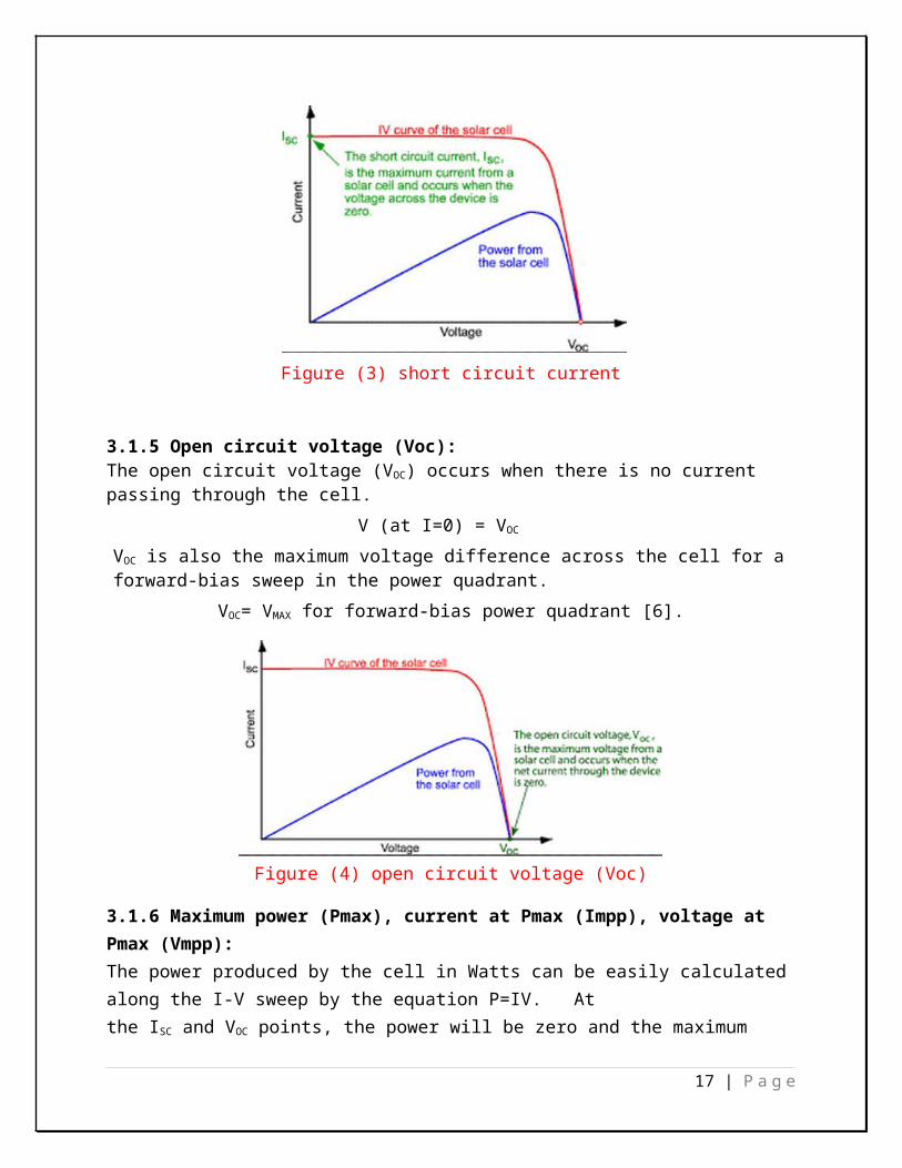
3.1.4 Short circuit current (Isc):The short circuit current ISC corresponds to the short circuit condition when the impedance is low and is calculated when the voltage equals 0.
I (at V=0) = ISC ISC occurs at the beginning of the forward-bias sweep and is the maximum current value in the power quadrant. For an ideal cell, this maximum current value is the total current produced in the solar cell by photon excitation.
ISC = IMAX = Iℓ for forward-bias power quadrant [6].
Figure (3) short circuit current
3.1.5 Open circuit voltage (Voc):The open circuit voltage (VOC) occurs when there is no current passing through the cell.
V (at I=0) = VOC
13 | P a g e

VOC is also the maximum voltage difference across the cell for a forward-bias sweep in the power quadrant.
VOC= VMAX for forward-bias power quadrant [6].
Figure (4) open circuit voltage (Voc)
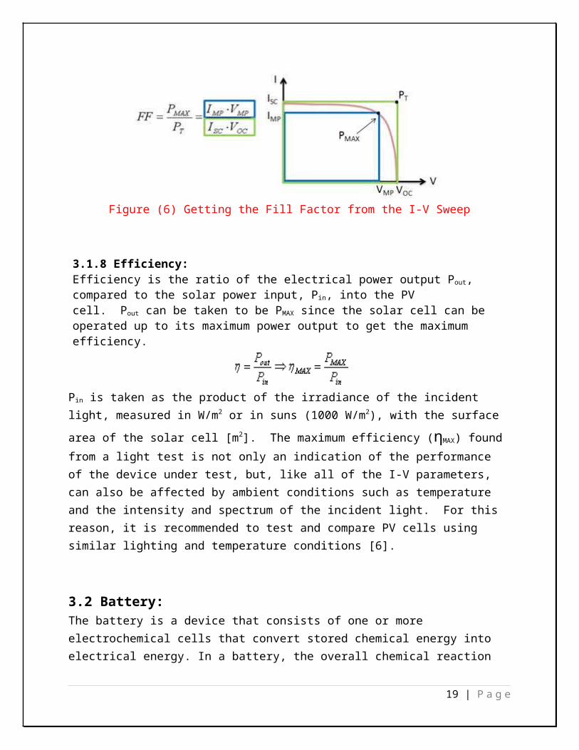
3.1.6 Maximum power (Pmax), current at Pmax (Impp), voltage at Pmax (Vmpp):The power produced by the cell in Watts can be easily calculated along the I-V sweep by the equation P=IV. At the ISC and VOC points, the power will be zero and the maximum value for power will occur between the two. The voltage and current at this maximum power point are denoted as VMP and IMP respectively [6].
Figure (5) Maximum Power for an I-V Sweep
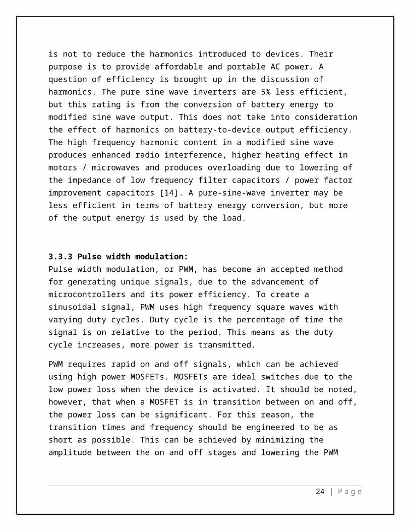
3.1.7 Fill factor (FF):The Fill Factor (FF) is essentially a measure of quality of the solar cell. It is calculated by comparing the maximum power to the theoretical power (PT) that would be output at both the open circuit voltage and short circuit current together. FF can also be interpreted graphically as
14 | P a g e
the ratio of the rectangular areas depicted in Figure (6). A larger fill factor is desirable, and corresponds to an I-V sweep that is more square-like. Typical fill factors range from 0.5 to 0.82. Fill factor is also often represented as a percentage [6].
Figure (6) Getting the Fill Factor from the I-V Sweep
3.1.8 Efficiency: Efficiency is the ratio of the electrical power output Pout, compared to the solar power input, Pin, into the PV cell. Pout can be taken to be PMAX since the solar cell can be operated up to its maximum power output to get the maximum efficiency.
Pin is taken as the product of the irradiance of the incident light, measured in W/m2 or in suns
(1000 W/m2), with the surface area of the solar cell [m2]. The maximum efficiency (ηMAX) found from a light test is not only an indication of the performance of the device under test, but, like all of the I-V parameters, can also be affected by ambient conditions such as temperature and the intensity and spectrum of the incident light. For this reason, it is recommended to test and compare PV cells using similar lighting and temperature conditions [6].
3.2 Battery:The battery is a device that consists of one or more electrochemical cells that convert stored chemical energy into electrical energy. In a battery, the overall chemical reaction is divided by two physically and electrically separated processes, such as one is an oxidation process at the battery negative electrode wherein the valence of at least one species becomes more positive, and the other is a reduction process at the battery positive electrode wherein the valence of at least one species becomes more negative. The battery functions by providing separate pathways for electrons and ions to move between the site of oxidation and the site of reduction. The electrons will pass through the external circuit, where it can provide useful work, for example power a portable device such as cellular phone or electric vehicle. While, the ions pass though the ionic-ally conducting and electronically insulating electrolyte that lies between the two
15 | P a g e

electrodes inside the battery. Therefore, the ionic current is separated from the electronic current, which can be easily controlled by a switch or a load in the external circuit. When a battery is discharged, an electrochemical oxidation reaction proceeds at the negative electrode and passes electrons into the external circuit, and a simultaneous electrochemical reduction reaction proceeds at the positive electrode and accepts electrons from the external circuit, thereby completing the electrical circuit. The change from electronic current to ionic current occurs at the electrolyte or electrode interface. When one attempts to recharge a battery by reversing the direction of electronic current flow, an electrochemical reduction reaction will proceed at the negative electrode, and an electrochemical oxidation reaction will proceed at the positive electrode [7].
3.3 Inverter:Power inverter is a device that converts electrical power from DC form to AC form using electronic circuits. It is typical application is to convert battery voltage into conventional household AC voltage allowing you to use electronic devices when an AC power is not available. Inverters have become more and more common over the past several years as support for self-sufficient solar power has increased. Because solar power is comes as a DC source, it requires an inverter before it can be used as general power [8].
3.3.1 Direct versus alternating current:In the world today, there are currently two forms of electrical transmission, direct current (DC) and alternating current (AC) systems, each with their own advantages and disadvantages. DC power is simply the application of a constant voltage across a load resulting in a constant current. A battery is the most common power source for DC along with several forms of power generation. This is widely used in digital circuitry as it provides constant high and low values which represent the basic 1 and 0 bits used by computers. Thomas Edison, inventor of the light bulb, was the first to transmit electricity commercially using DC power lines. It was not capable of transmission over long distances because the technology did not exist to step-up the voltage along the transmission path over which the power would dissipate. The equation below demonstrates how high voltage is necessary to decrease power loss [9].
V = I*R
P = I 2∗R = V 2/R
When the voltage is increased, the current decreases and concurrently the power loss decrease exponentially. Therefore, high voltage transmission decreases power loss. AC power was found
16 | P a g e
to be much more efficient at transmitting power as it alternates between two voltages at a specific frequency, making it easier to either step up or down using a transformer [9]. Today, electrical transmission is based mostly of AC power, supplying homes and businesses with 230V AC power at 50Hz.While DC power is used in many digital applications, AC power also used in many other applications such as in power tools, televisions, radios, medical devices, and lighting. Therefore, it is necessary to have an efficient means of transforming DC to AC and vice versa. Without this ability, people would be restricted to using devices that only works on the power that is supplied to them [9].
3.3.2 Classification of inverters:
1) Current fed inverter (CFI) – input current remains constant.2) Voltage fed inverter (VFI) – input voltage remains constant.3) Variable DC linked inverter – input voltage is controlled.
There are basically three kinds of VFI power inverter out of which, the first set of inverters made, which are now obsolete, produced a Square Wave signal at the output.
Square wave inverter: Square wave inverter produces a square wave by switching the DC source at equal magnitude in opposite direction across a load at set frequencies. They are rarely used because many devices utilize timing circuits that rarely on input power waveform for a clock timer [10].
Pure sine wave: Pure sine wave inverter simulates precisely the AC power that is delivered by a wall socket. It introduces the least amount of harmonics into an electrical devices but it’s also the most expensive method because of the extra components and design required to produce the output. Its main advantage is that it can power all devices [11].
17 | P a g e
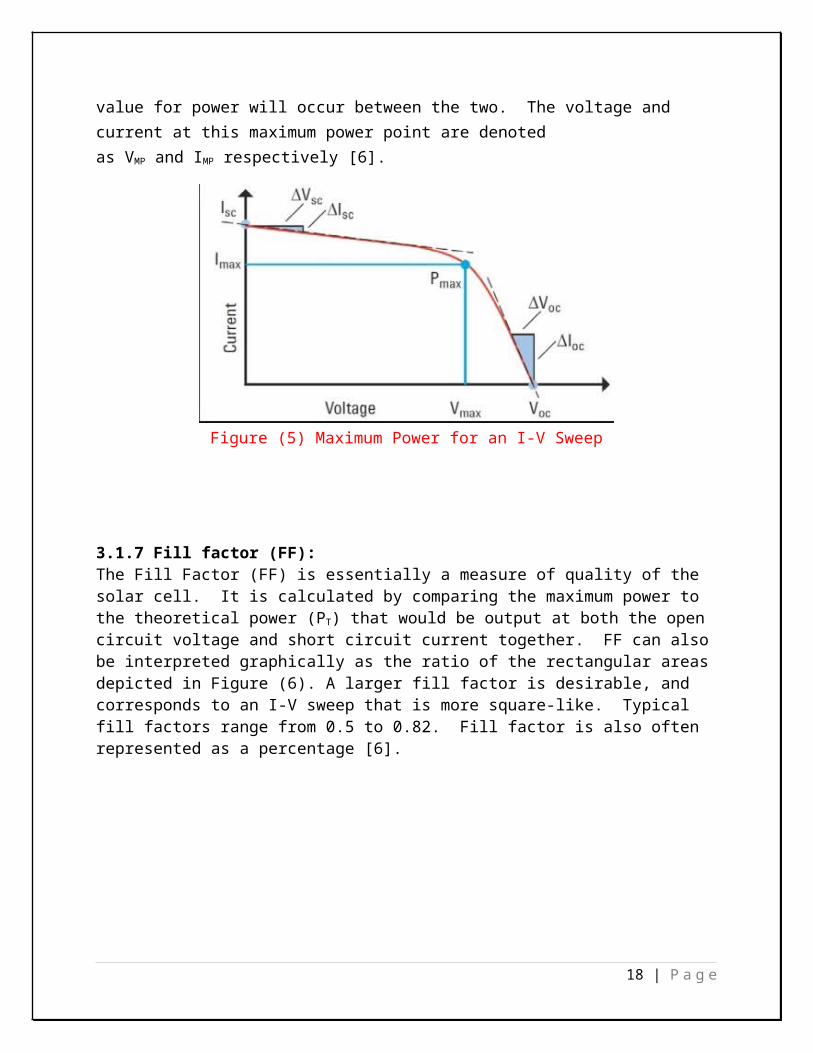
Figure (7) types of inverter
Modified sine wave Modified sine wave inverter emulates a sine wave. It introduces a dead time in a normal square wave output. The wave is produced by switching the DC source between three values at set frequencies thus produces fewer harmonics than square wave [12]. It provides a cheap and easy solution of powering devices that need AC power. Its main drawbacks are that not all device that are not resistant to the distortion of the signal like medical equipment and computers work properly on it [13]. It should be noted that modified-sine wave inverters are not rated for Total Harmonic Distortion (THD). Rating a modified-sine wave inverter for harmonic distortion would be useless, for their intended use is not to reduce the harmonics introduced to devices. Their purpose is to provide affordable and portable AC power. A question of efficiency is brought up in the discussion of harmonics. The pure sine wave inverters are 5% less efficient, but this rating is from the conversion of battery energy to modified sine wave output. This does not take into consideration the effect of harmonics on battery-to-device output efficiency. The high frequency harmonic content in a modified sine wave produces enhanced radio interference, higher heating effect in motors / microwaves and produces overloading due to lowering of the impedance of low frequency filter capacitors / power factor improvement capacitors [14]. A pure-sine-wave inverter may be less efficient in terms of battery energy conversion, but more of the output energy is used by the load.
18 | P a g e
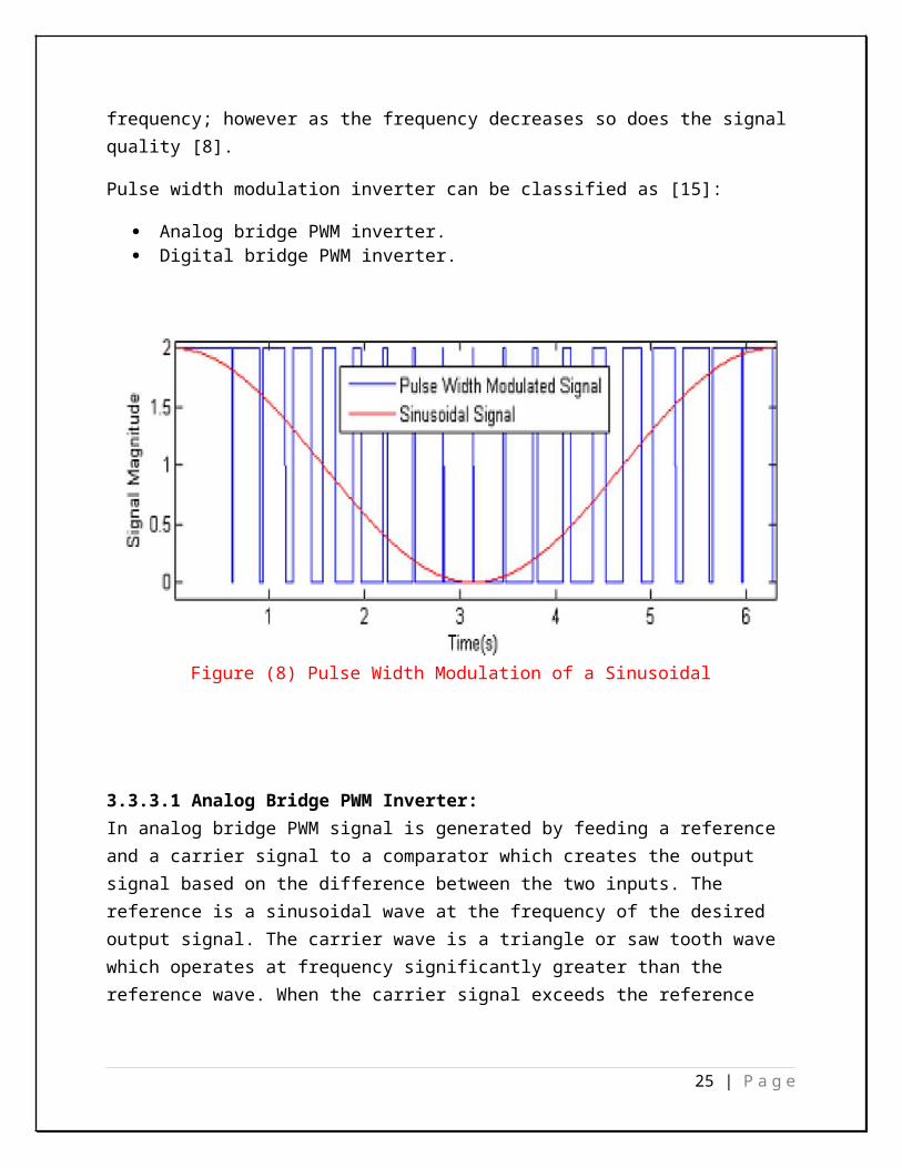
3.3.3 Pulse width modulation:Pulse width modulation, or PWM, has become an accepted method for generating unique signals, due to the advancement of microcontrollers and its power efficiency. To create a sinusoidal signal, PWM uses high frequency square waves with varying duty cycles. Duty cycle is the percentage of time the signal is on relative to the period. This means as the duty cycle increases, more power is transmitted.
PWM requires rapid on and off signals, which can be achieved using high power MOSFETs. MOSFETs are ideal switches due to the low power loss when the device is activated. It should be noted, however, that when a MOSFET is in transition between on and off, the power loss can be significant. For this reason, the transition times and frequency should be engineered to be as short as possible. This can be achieved by minimizing the amplitude between the on and off stages and lowering the PWM frequency; however as the frequency decreases so does the signal quality [8].
Pulse width modulation inverter can be classified as [15]:
Analog bridge PWM inverter. Digital bridge PWM inverter.
Figure (8) Pulse Width Modulation of a Sinusoidal
19 | P a g e

3.3.3.1 Analog Bridge PWM Inverter:In analog bridge PWM signal is generated by feeding a reference and a carrier signal to a comparator which creates the output signal based on the difference between the two inputs. The reference is a sinusoidal wave at the frequency of the desired output signal. The carrier wave is a triangle or saw tooth wave which operates at frequency significantly greater than the reference wave. When the carrier signal exceeds the reference the output is at high state and when the reference exceeds the carrier the output is at low state [16].
Advantages:The level of the inverter output can be adjusted in a continuous range and the through put delay is negligible [16].
Disadvantages:Analog components output characteristics change with the temperature and time.
Analog component circuitry is complex and bulky and they are nonprogrammable, hence not flexible [16].
3.3.3.2 Digital Bridge PWM Inverter:Also known as microcontroller based power inverter. it makes the controller free from disturbance and drift but the performance is not very high due to its speed limitation. However, to reduce through put delay some microcontroller retrieve switching pattern straight from memory so calculation can be minimized, but this technique demands more memory. This drawback can be eliminated by switching patterns executing simple control algorithms. With availability of advanced microcontroller and DSP (digital signal processor) controller that has advanced features like inbuilt PWM generator, event manager, time capture unit, dead time delay generator, watch dog timer along with high clock frequency, the limitation of speed associated with microcontroller can be neglected to some extent [16].
Advantages:The inverter is not prone to external disturbance like temperature. It’s simple and cost effective technique of implementing single phase AC voltage controller [16].
Disadvantages:Even after using simple control algorithms, sometimes through put delay may be substantial [16].
3.4 Transformer:A transformer is an electrical device which is used for changing (transform) the AC voltages. It is based on the principal of mutual induction. A transformer is essentially an AC. device. It
20 | P a g e

cannot work on AC. A transformer changes only AC voltages/currents.Transformer cross-section showing primary and secondary windings is a few inches tall (approximately 10 cm) [17].
There are two types of transformer.
Step up transformer. Step down transformer.
A transformer which increases the AC voltage is called step up transformer.A transformer which decreases the AC voltage is called step down transformer.
There are many types of energy loses in transformer. Major sources of energy lose are: copper loss, iron loss, leakage of magnetic flux, hysteresis loss and magnetostriction. We cannot obtain full input power as output power because of energy loses. Output power in a transformer is around 90% of the input power [17].
Chapter.4: MethodologyAs mentioned earlier that our project is working on converting the sunlight collected by the solar panel to an electrical power to supply a refrigerator, so we worked in many steps to achieve this converting.
4.1 Inverter design:A DC-AC power inverter is a circuit which modifies an input non-varying direct current (DC) to an alternating current (AC) of a specified voltage and frequency, and a regulated DC voltage. In the case of our project, the input DC voltage source will be a battery of 12V. As such, the DC voltage will likely be inconsistent, and considerations will need to be made in order to produce the desired output. This desired AC output is a 230V, 50Hz pure sine wave.
21 | P a g e

Figure (9) Inverter block diagram
4.1.1 Elements of Inverter:
4.1.1.1 Arduino NANO:The main component of this inverter is the arduino as it is used to generate control signals. The theory of encoding a sine wave with a PWM signal is relatively simple. A sine wave is needed for the reference that will dictate the output, and a triangle wave of higher frequency is needed to sample the reference and actuate the switches. Since the control technique which will be used is a sinusoidal pulse width modulated was chosen to generate required signal. Pins A1 and A2 are output pin for sinusoidal pulse width modulation.
22 | P a g e

4.1.1.1.1 Arduino NANO pins layout:
Figure (10) Arduino NANO pins layout
Table (1) Arduino Nano pins
4.1.1.1.2 Generating control signal:The arduino is tasked with generating four control signals that are used as inputs to the Mosfet driver. They are two 50 Hz square wave and two 2-level pulse width modulated at 180 degrees out of phase.
23 | P a g e
4.1.1.1.3 Arduino coding:Arduino language was used to write the code needed to program. The code was built using arduino 1.6.6 compiler to produce HEX file which is burned to arduino and loaded to proteus for simulation.
4.1.1.1.4 Arduino operating voltage:We used a voltage regulator (LM7805) to give 5V to operate the arduino.
Figure (11) LM7805
In order to have stable 5V at the output pin of the voltage regulator (pin3) the input voltage that becomes to pin1 should be between 7.4V to 24V.We fed this voltage regulator by battery voltage
which is 12V. Depending in current consumption the appropriate type of voltage regulator LM7805 was used.
Figure (12) voltage regulator circuit
24 | P a g e
4.1.1.2 H-Bridge:
Figure (13) single phase H-Bridge
An H-Bridge or full bridge converter is a switching configuration composed of four switches in this case MOSFETs in an arrangement that resembles an H [12]. By controlling which switches are closed at any given moment, the voltage across the load can be either positive, negative, or zero.
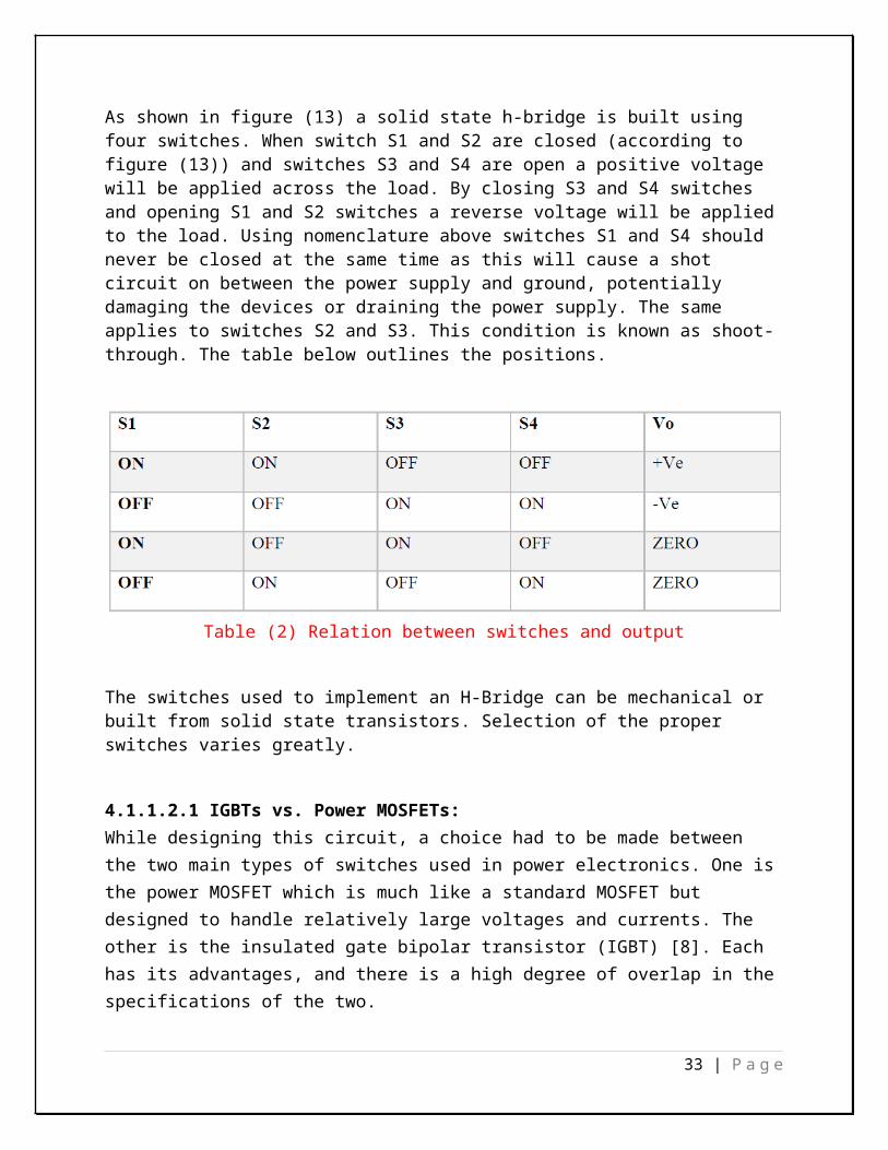
As shown in figure (13) a solid state h-bridge is built using four switches. When switch S1 and S2 are closed (according to figure (13)) and switches S3 and S4 are open a positive voltage will be applied across the load. By closing S3 and S4 switches and opening S1 and S2 switches a reverse voltage will be applied to the load. Using nomenclature above switches S1 and S4 should never be closed at the same time as this will cause a shot circuit on between the power supply and ground, potentially damaging the devices or draining the power supply. The same applies to switches S2 and S3. This condition is known as shoot-through. The table below outlines the positions.
25 | P a g e
Table (2) Relation between switches and output
The switches used to implement an H-Bridge can be mechanical or built from solid state transistors. Selection of the proper switches varies greatly.
4.1.1.2.1 IGBTs vs. Power MOSFETs:While designing this circuit, a choice had to be made between the two main types of switches used in power electronics. One is the power MOSFET which is much like a standard MOSFET but designed to handle relatively large voltages and currents. The other is the insulated gate bipolar transistor (IGBT) [8]. Each has its advantages, and there is a high degree of overlap in the specifications of the two.
IGBTs tend to be used in very high voltage applications, nearly always above 200V, and generally above 600W. They do not have the high frequency switching capability of MOSFETs, and tend to be used at frequencies lower than 29 kHz. They can handle high currents, are able to output greater than 5kW, and have very good thermal operating ability, being able to operate properly above 100 Celsius. One of the major disadvantages of IGBTs is their unavoidable current tail when they turn off. Essentially, when the IGBT turns off, the current of the gate transistor cannot dissipate immediately, which causes a loss of power each time this occurs. This tail is due to the very design of the IGBT and cannot be remedied [8].
IGBTs also have no body diode, which can be good or bad depending on the application. IGBTs tend to be used in high power applications, such as uninterruptible power supplies of power higher than 5kW, welding, or low power lighting [12].
Power MOSFETS have a much higher switching frequency capability than do IGBTs, and can be switched at frequencies higher than 200 kHz. They do not have as much capability for high voltage and high current applications, and tend to be used at voltages lower than 250V and less than 500W. MOSFETs do not have current tail power losses, which makes them more efficient than IGBTs. Both MOSFETs and IGBTs have power losses due to the ramp up and ramp down of the voltage when turning on and off (dV/dt losses). Unlike IGBTs, MOSFETs have body diode [12].
26 | P a g e

Generally, IGBTs are the sure bet for high voltage, low frequency (>1000V, <20 kHz) uses and MOSFETs are ideal for low voltage, high frequency applications (<250V, >200 kHz). In between these two extremes is a large grey area. In this area, other considerations such as power, percent duty cycle, availability and cost tend to be the deciding factors. Since this project is about design of a 600W inverter, with a 340VDC bus (ideally), and a switching frequency of 5 kHz MOSFET is the ideal choice, in spite of MOSFET switches having high ON state resistance and conduction losses. Also MOSFET being a voltage controlled device, it can be driven directly from CMOS or TTL logic and the same gate signal can be applied to diagonally opposite switches since the gate drive current required is very low. If our system was a larger, commercial application with a high power output, IGBTs would be the choice [8].
4.1.1.2.2 Enhanced N-channel vs enhanced P-channel MOSFETS:The use of P-Channel MOSFETs on the high side and N-Channel MOSFETs on the low side is easier, but using all N-Channel MOSFETs and a FET driver, lower “on” resistance can be obtained resulting in reduced power loss. This requires a more complex circuit since the gate of the high side Mosfet must be driven positive with respect to Vs bus voltage to turn on the Mosfet [18].
4.1.1.2.3 MOSFETs Characteristic:
In our project enhanced n-channel Mosfet was chosen for both high side and low side switches of the h-bridge. For the Mosfet to carry drain current Id (on state) a channel between the drain and source must be created. This occurs when drain to source Vgs voltage exceeds the device threshold (Vgs>Vth). Once the channel is induced the Mosfet can operate in either triode region (drain current proportional to channel resistance) or the saturation region (constant drain current). The gate to drain voltage Vgs determines whether the induced channel enters pitch-off or remains in triode region. When used as a switching device only triode and cut-off region are utilized. The device will operate at cut-off (off state) when gate to source voltage Vgs is less than threshold voltage Vth (Vgs<Vth) [15]. Figure (14a) shows schematic symbol, figure (14b) shows its drain characteristic and figure (14c) shows drain current flows only when Vgs exceeds threshold voltage.
Triode region: Vds<Vgs-Vth Saturation region : Vds>Vgs-Vth Cut-off region : Vgs<Vth
27 | P a g e
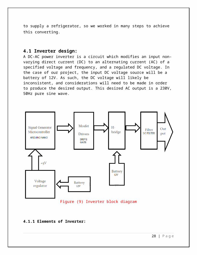
Figure (14) N channel MOSFET characteristic
4.1.1.3 MOSFET Driver:As stated in the previous section, it is beneficial to use N-channel MOSFETs as the high side switches as well as the low side switches because they have a lower ‘ON’ resistance and therefore less power loss. However, to do so, the drain of the high side device is connected to 12V DC power which is to be inverted into the 12V AC power. This is a problem because the 12V is the highest voltage in the system and in order for the switch to be turned on the voltage at the gate terminal must be 10V higher than the drain terminal voltage [19, 20]. Therefore, to drive MOSFETs in the H-Bridge MOSFET driver IC is used with a bootstrap capacitor specifically designed for driving a half-bridge. After considering various IC options, the ideal choice was the IR2110, which is rated at 600V, with a gate driving current of 2A and a gate driving voltage of 10-20V. The turn on and turn off times are 120ns and 94ns respectively [21].
The MOSFET driver operates from a signal input given from the microcontroller and takes its power from the battery voltage supply that the system uses. The driver is capable of operating both the high side and low side devices, but in order to get the extra 10V for the high side device, an external bootstrap capacitor is charged through a diode from the 18V power supply when the device is off. Because the power for the driver is supplied from the low voltage source, the power consumed to drive the gate is small. When the driver is given the signal to turn on the high side device, the gate of the MOSFET has an extra boost in charge from the bootstrap capacitor, surpassing the needed 10V to activate the device and turning the switch on [22].
28 | P a g e

Figure (15) IR2110 connection
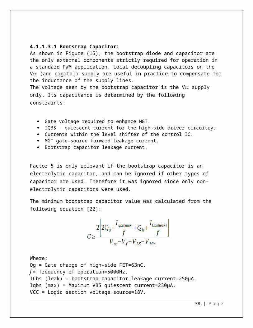
4.1.1.3.1 Bootstrap Capacitor:As shown in Figure (15), the bootstrap diode and capacitor are the only external components strictly required for operation in a standard PWM application. Local decoupling capacitors on the VCC (and digital) supply are useful in practice to compensate for the inductance of the supply lines. The voltage seen by the bootstrap capacitor is the VCC supply only. Its capacitance is determined by the following constraints:
Gate voltage required to enhance MGT. IQBS - quiescent current for the high-side driver circuitry. Currents within the level shifter of the control IC. MGT gate-source forward leakage current. Bootstrap capacitor leakage current.
Factor 5 is only relevant if the bootstrap capacitor is an electrolytic capacitor, and can be ignored if other types of capacitor are used. Therefore it was ignored since only non-electrolytic capacitors were used.
The minimum bootstrap capacitor value was calculated from the following equation [22]:
29 | P a g e

Where: Qg = Gate charge of high-side FET=63nC. f = frequency of operation=5000Hz.ICbs (leak) = bootstrap capacitor leakage current=250μA.Iqbs (max) = Maximum VBS quiescent current=230μA. VCC = Logic section voltage source=18V. Vf = Forward voltage drop across the bootstrap diode=0.4V.VLS = Voltage drop across the low-side FET or load=1.8V. VMin = Minimum voltage between VB and VS=10V. Qls = level shift charge required per cycle (typically 5nC for 500 V/600 V MGDs and 20nC for 1200 V MGDs).
The values substituted into this equation were found either in driver datasheet for IR2110 IC or IRF840 MOSFET datasheet. Using these numbers minimum bootstrap capacitance value was calculated as:
The capacitor value obtained from the above equation is the absolute minimum required, however due to nature the bootstrap circuit operation, a low value of capacitor can lead to overcharging which could in turn damage the IC. Therefore to minimize the risk of overcharging and further reduce ripple on the Vds voltage the capacitor value obtained is multiplied by a factor of 15 to get a capacitor value of 1μF [22].
4.1.1.3.2 Bootstrap Diode:The bootstrap diode must be able to block the full voltage seen in the specific circuit and is about equal to the voltage across the power rail. The current rating of the diode is the product of gate charge times switching frequency. The high temperature reverse leakage characteristic of this diode can be an important parameter in those applications where the capacitor has to hold the charge for a prolonged period of time. For the same reason it is important that this diode have an
30 | P a g e

ultra-fast recovery to reduce the amount of charge that is fed back from the bootstrap capacitor into the supply [22].
In order to improve decoupling decoupling capacitors has to be connected directly across the VCC and COM pins as shown in figure (15).
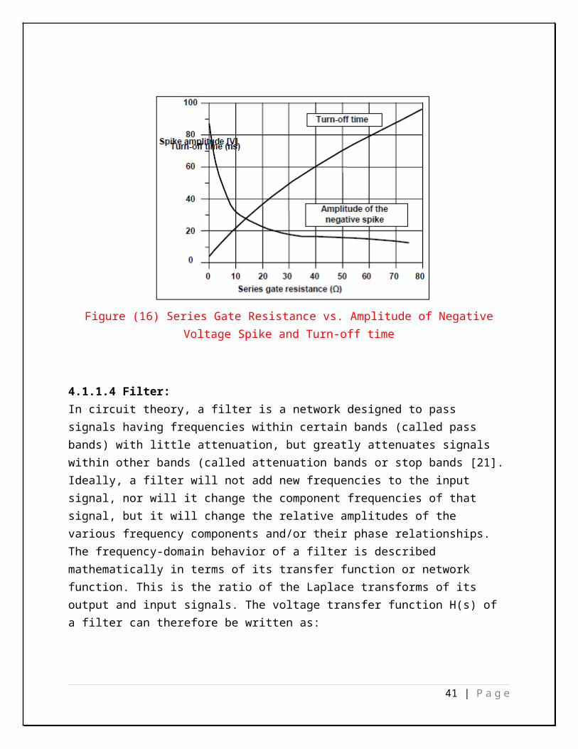
4.1.1.3.3 Gate resistor:Driving MOS-gated power transistors directly from the driver can result in unnecessarily high switching speeds. Increasing the value of the series gate resistor, results in a rapid decrease of the amplitude of the negative spike, while the turn-off time is a linear function of the series gate resistance. Selecting a resistor value just right from the “knee” in Figure (16) provides a good trade-off between the spike amplitude and the turn-off speed the di/dt may have to be reduced by reducing the switching speed by means of the gate resistor [22]. A graph of the negative spike and the turn-off time versus series gate resistance is shown in Figure (16). The layout should also minimize the stray inductance in the charge/discharge loops of the gate drive to reduce oscillations and to improve switching speed and noise immunity, particularly the “dV/dt induced turn-on”. For this design resistor values of 20 ohms were chosen [22].
Figure (16) Series Gate Resistance vs. Amplitude of Negative Voltage Spike and Turn-off time
4.1.1.4 Filter:In circuit theory, a filter is a network designed to pass signals having frequencies within certain bands (called pass bands) with little attenuation, but greatly attenuates signals within other bands
31 | P a g e

(called attenuation bands or stop bands [21]. Ideally, a filter will not add new frequencies to the input signal, nor will it change the component frequencies of that signal, but it will change the relative amplitudes of the various frequency components and/or their phase relationships. The frequency-domain behavior of a filter is described mathematically in terms of its transfer function or network function. This is the ratio of the Laplace transforms of its output and input signals. The voltage transfer function H(s) of a filter can therefore be written as:
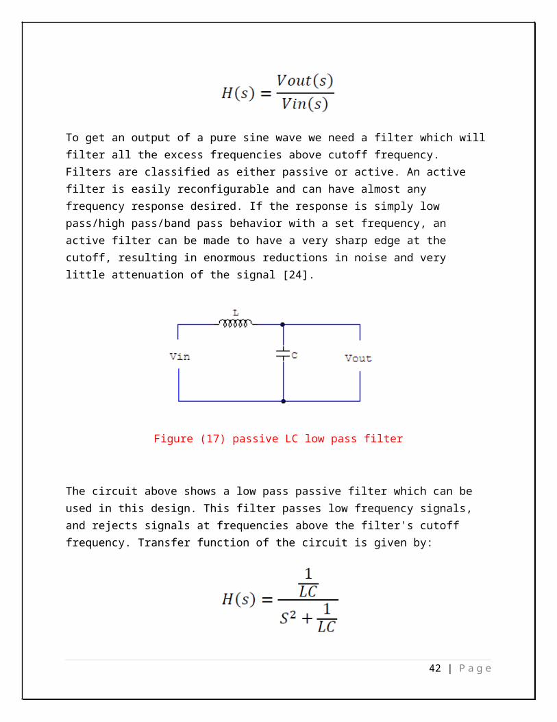
To get an output of a pure sine wave we need a filter which will filter all the excess frequencies above cutoff frequency. Filters are classified as either passive or active. An active filter is easily reconfigurable and can have almost any frequency response desired. If the response is simply low pass/high pass/band pass behavior with a set frequency, an active filter can be made to have a very sharp edge at the cutoff, resulting in enormous reductions in noise and very little attenuation of the signal [24].
Figure (17) passive LC low pass filter
The circuit above shows a low pass passive filter which can be used in this design. This filter passes low frequency signals, and rejects signals at frequencies above the filter's cutoff frequency. Transfer function of the circuit is given by:
32 | P a g e
It is easy to see by inspection that this transfer function is a second order and by equating this equation with that of a standard second order:
Cutoff frequency will be given by:
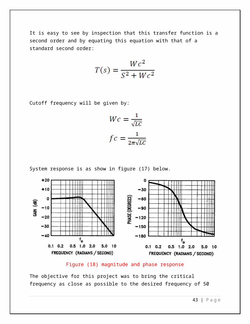
System response is as show in figure (17) below.
Figure (18) magnitude and phase response
The objective for this project was to bring the critical frequency as close as possible to the desired frequency of 50 Hz, removing other harmonics that crop up within the system. The issue with the filter is one of component size and availability. The slower the cutoff frequency, the greater the capacitance and inductance required to properly create the filter. Therefore, filter
33 | P a g e

design becomes a tradeoff between the effectiveness of the filter and the cost and size of the components.
4.2 Choosing the transformer:In our project we need a step-up transformer to convert the AC voltage from 12V which became from the inverter to 230V to supply the refrigerator, so we used a transformer with specifications 12/230V with 50VA.
4.3 Choosing the battery:The solar panel that we used gives 12VDC with 53W, so we used a battery with specifications 12V and with capacity 7.2Amp.hour.
Solar panel gives current as the following:
I = P/V = 53/12 = 4.42.
So the battery will charge during:Tch = 7.2/4.42 = 1.63 hours (an hour and 37.8 minutes) to charger the battery.
4.4 simulation:
4.4.1 Circuit diagram:
34 | P a g e

Figure (19) Inverter circuit
4.4.2 Simulation Results:
4.4.2.1 Arduino output:50Hz Pulse Width Modulation signal from pins (A1 & A2).
As mentioned earlier the output of pins (A1 & A2) which are used to drive one side of H-bridge should be 180 degrees out of phase and they are as shown below in figure (19).
35 | P a g e

Figure (20) pulse width modulation signal generated from Arduino
4.4.2.2 H-Bridge output:The next simulation step includes the MOSFET driver, IR2110 and the H-bridge. The driver’s main purpose is to keep the gate voltage 10V above the source when the MOSFET is enabled. The expected response of the driver is approximately 100ns; meaning that after the MOSFET driver is enabled it will take 100ns to drive the gate voltage to 10V with respect to the source.
36 | P a g e

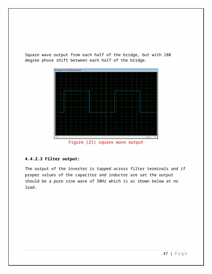
Square wave output from each half of the bridge, but with 180 degree phase shift between each half of the bridge.
Figure (21) square wave output
4.4.2.3 Filter output:
The output of the inverter is tapped across filter terminals and if proper values of the capacitor and inductor are set the output should be a pure sine wave of 50Hz which is as shown below at no load.
Figure (22) output of the inverter at no load
37 | P a g e
Chapter.5: Results and Discussion
5.1 Inverter circuit:After simulation and determination of specifications of the overall design, a prototype is built of the final circuit of the battery and the inverter as shown below in figure (22).
Figure (23) Inverter circuit
38 | P a g e

5.2 Outputs:
5.2.1 Arduino outputs:Laboratory oscilloscope was used to observe the output waveform the PWM outputs of the arduino.
Figure (24) PWM waves from the Arduino
The yellow one is showing the first PWM wave and the blue one is showing the second PWM wave. There is a phase shift between them by 180 degree.
39 | P a g e

5.2.2 H-Bridge outputs:
5.2.2.1 first half of H-Bridge output:The figure (24) below is showing the first half H-Bridge square wave output.
Figure (25) square wave from the first half H-Bridge
5.2.2.2 second half of H-Bridge output:The figure (25) below is showing the second half of the H-Bridge square wave. This wave has shifted by 180 degree.
Figure (26) square wave from the second half H-Bridge
40 | P a g e
5.2.2.3 LC Filter output:Figure (26) below is showing the overall output of the inverter after the LC Filter at no load.
Figure (27) sine wave LC Filter output
The inverter gives 12Vpp and its ready to enter the transformer to give 220V.
Each LC Filter built by using inductor with two capacitors, the value of the inductor is 0.68mH and each capacitor has the value 2200uF. We connected the two capacitors in parallel to give
C = C1+C2 = 2200+2200 = 4400uF.
41 | P a g e
5.3 Characteristics of Inverter:
5.3.1 Sine wave output:Most DC-AC inverters deliver a modified sine wave output voltage because it’s cheap to produce and it has a high conversion efficiency, but the problem is that the alternating pulses Output waveform is relatively rich in harmonics. Due to this problem some appliances cannot use this type of inverter supply waveform, hence the need for a pure sine wave inverter like the one designed in this project. It is therefore recommended to all appliances.
5.3.2 Total harmonic distortion:The total harmonic distortion, or THD, of a signal is a measurement of the harmonic distortion present and is defined as the ratio of the sum of the powers of all harmonic components to the power of the fundamental frequency . THD is used to characterize the power quality of electric power systems.
Since power is given by voltage squared divided by resistance the above equation can be written as the ratio of sum of harmonic voltages divided by fundamental voltage.
5.3.3 Voltage spikes:When used to drive inductive load impedance inverter may develop voltage spikes due to back EMF. These spikes can be transformed back into the H-bridge, where they have the potential to damage the MOSFETs and their driving circuitry. It’s for this reason that in this design transistors with build in diode were used to conduct heavily as soon as the voltage rises excessively protecting the MOSFETs from being damaged by these back voltages and hence the modeled inverter can be said to be save to use with inductive load.
42 | P a g e
5.3.4 Capacitive load:As this inverter is a pure sine wave harmonics of high frequency have been removed altogether and when it’s used with a capacitive load the impedance is as calculated. The problem with other types of inverter is that due to high frequency harmonics the capacitive impedance is lowered hence much current is drawn from the inverter which may exceed the rated current.
5.3.5 Frequency stability:Most appliances and tools designed for mains power can tolerate a small variation in supply frequency, but they can malfunction, overheat or even be damaged if the frequency changes significantly. To avoid such problems, this inverter uses PIC microcontroller programmed to use quartz crystal oscillator and divider system to generate the master timing for the MOSFET drive pulses. These ensure that the output voltage remains at 50Hz frequency.
5.3.6 Operating Temperature:Rise in temperature is brought by high frequency switching of MOSFET which dramatically decreases the power output the inverter. In order to maintain a low temperature all MOSFETs and voltage regulators are mounted with heat sinks however for commercial design it is recommended to incorporate fan to circulate air within the closed box.
Chapter.6: Conclusions and RecommendationsThe objective of our project was to produce an electrical energy from the sunlight that collected by solar array. Battery used to store the DC power to prepare this DC power to invert it into AC power then using a step-up transformer to prepare this AC power to the refrigerator, supplying this refrigerator by alternative energy instead of using traditional sockets.
Conclusion can be drawn from this work are: Output of the solar array was 12 volt with 53W stored in the battery. Output waveform frequency of the inverter was found to be satisfactory at 50Hz
equivalent of standard Palestinian power system. Sine pulse width modulation circuit is much simplified by using Arduino. In addition with the high programming flexibility the design of the switching pulses can
be altered without further changes on the hardware.
43 | P a g e

There are a few changes that need to be worked on for future work in the inverter circuit. Proper inductor is recommended, iron core inductor that has small copper resistance which will increase the efficiency of the inverter. In addition, I would recommend even the prototype boards in enclosures to avoid unwanted contact with the high power sources. Also hardware designed that isolates the load from the supply in case of over voltages, under voltages and phase outs would be of great importance if this project is to be commercially produced in large scale.
44 | P a g e

References:
1) http://www.energybible.com/solar_energy/ . Last accessed November 29, 2015.
2) http://www.comet-me.org/press/ Last accessed November 29, 2015.
3) https://www.quantumbalancing.com/worldelectricity/electricityif.htm Last accessed November 29, 2015.
4) http://www.zoombd24.com/photovoltaic-cell/ . Last accessed November 29, 2015.
5) http://energyinformative.org/best-solar-panel-monocrystalline-polycrystalline-thin-film/ . Last accessed November 29, 2015.
6) http://www.ni.com/white-paper/7230/en/ . Last accessed November 29, 2015.
7) Bellis, Mary. 2008. History of the electric Battery.About.com. Last accessed November 29, 2015.
8) M. H. Rashid, “Power Electronics Circuits, Devices and Applications,” 3rd Edition, Prentice-Hall of India, Private limited, New-Delhi, 2004.Last accessed November 29, 2015.
9) John J. Grainger and William D. Stevenson, POWER SYSTEMS ANALYSIS McGraw-Hill, Inc.1994. Last accessed November 29, 2015.
10) Ian F. Crowley and Ho Fong Leung, “PWM Techniques: A Pure Sine Wave Inverter” Worcester Polytechnic Institute 2011.Last accessed November 29, 2015.
11) A. A. Mamun, M. F. Elahi, M. Quamruzzaman, M. U. Tomal, “Design and Implementation of Single Phase Inverter” International Journal of Science and Research (IJSR), India Online ISSN: 2319-7064 Volume 2 Issue 2, February 2013.Last accessed November 29, 2015.
45 | P a g e

12) Ian F. Crowley and Ho Fong Leung, “PWM Techniques: A Pure Sine Wave Inverter” Worcester Polytechnic Institute 2011.Last accessed November 29, 2015.
13) A.Ali Qazalbash, Awais Amin, Abdul Manan and Mahveen Khalid, “Design and Implementation of Microcontroller based PWM technique for Sine wave Inverter”, International Conference on Power engineering, Energy and Electrical Drives, POWERENG '09. 2009 pp.163-167, IEEE.Last accessed November 29, 2015.
14) Griffith, P. Designing Switching Voltage Regulators with the TL494. Dallas, Texas, USA: Texas Instruments. February 2005.Last accessed November 29, 2015.
15) S. A. Hari Prasad, B. S. Kariyappa, R. Nagaraj, S. K.Thakur “Micro Controller Based Ac Power Controller” Wireless Sensor Network, 2009, 2, 61-121.Last accessed November 29, 2015.
16) www.scirp.org/journal/PaperDounload.aspx?paperID=521.Last accessed November 29, 2015.
17) http://www.ukessays.com/dissertation/literature-review/the-applications-and-uses-of-transformer.php.Last accessed November 29, 2015.
18) Gopinath.G, PG and A.Arikesh “Development of Three Step Charging H-Bridge based Sine wave Inverter” International Journal of Advanced Trends in Computer Science and Engineering, Vol.2 , No.2, Pages : 149-153 (2013)Last accessed November 29, 2015.
19) Principles and Application of Electrical Engineering McGraw hill.Last accessed November 29, 2015.
20) IRF840, SiHF840 datasheet power Mosfet by Vishay.Last accessed November 29, 2015.
21) IR2110 (-1-2)(S)PbF/IR2113(-1-2)(S)PbF’ “HIGH AND LOW SIDE DRIVER” Data Sheet No. PD60147 rev.U International Rectifier.Last accessed November 29, 2015.
46 | P a g e
22) Application note AN-978, “HV Floating MOS-gate driver ICs” by International Rectifier.Last accessed November 29, 2015.
23) John Bird, “electrical circuit theory and technology” Revised second edition, Newnes Oxford 2003.Last accessed November 29, 2015.
24) Application note AN-779, “a basic introduction to filters-active, passive and switched capacitors,” National semiconductor, April 1991.Last accessed November 29, 2015.
47 | P a g e