solar energy materials & solar cells - centre national de ... · facile metallization of...
TRANSCRIPT
Solar Energy Materials & Solar Cells 102 (2012) 26–30
Contents lists available at SciVerse ScienceDirect
Solar Energy Materials & Solar Cells
0927-02
doi:10.1
n Corr
E-m
journal homepage: www.elsevier.com/locate/solmat
Facile metallization of dielectric coatings for plasmonic solar cells
S. Bastide a,n, T. Nychyporuk b, Z. Zhou b, A. Fave b, M. Lemiti b
a Institut Chimie et Materiaux Paris-Est (ICMPE), CNRS-UMR-7182, UPE, 2-8 rue Henri Dunant, 94320 Thiais, Franceb Universite de Lyon, Institute for Nanotechnologies of Lyon (INL), INL-UMR5270, CNRS, INSA de Lyon, 7 avenue Jean Capelle, Bat. Blaise Pascal, Villeurbanne, F-69621, France.
a r t i c l e i n f o
Available online 3 December 2011
Key words:
Metal nanoparticles
Hydrogenated silicon nitride
Silicon oxide
Silicon nanoparticles
Electroless metal deposition
Plasmonic solar cell
48/$ - see front matter & 2011 Elsevier B.V. A
016/j.solmat.2011.11.016
esponding author.
ail address: [email protected] (S. Bastide).
a b s t r a c t
Electroless deposition of Ag nanoparticles on PECVD SiNx:H dielectric layers is a new straightforward
chemical bath process well adapted to the realization of plasmonic solar cells. Depending on the
stoichiometry, SiNx:H contains a certain number of Si nanoclusters embedded in the silicon nitride
matrix, that act as reducing agents for Ag ions in solution and thus allows the deposition of Ag
nanoparticles directly on the surface. We investigate the influence of the layer stoichiometry and
deposition parameters on the nucleation and growth of Ag nanoparticles, and show how they can be
adjusted to control the nanoparticle size and density. We also demonstrate that this facile metallization
process can be extended to PECVD SiOx layers, another dielectric coating of interest in photovoltaics.
& 2011 Elsevier B.V. All rights reserved.
1. Introduction
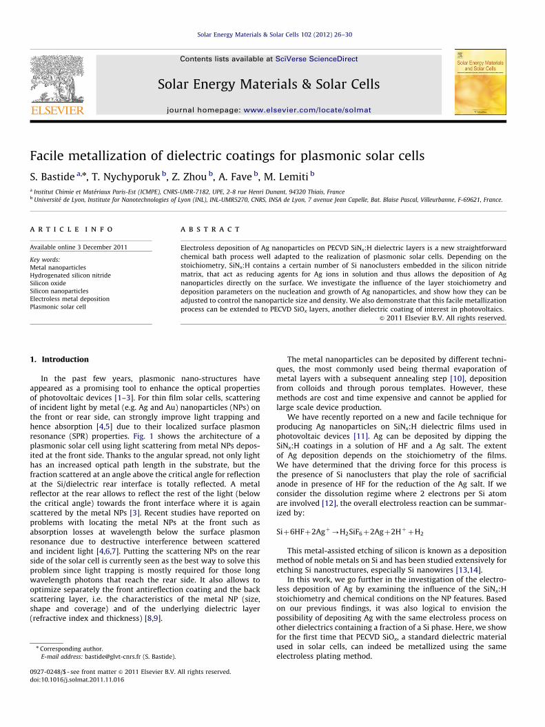
In the past few years, plasmonic nano-structures haveappeared as a promising tool to enhance the optical propertiesof photovoltaic devices [1–3]. For thin film solar cells, scatteringof incident light by metal (e.g. Ag and Au) nanoparticles (NPs) onthe front or rear side, can strongly improve light trapping andhence absorption [4,5] due to their localized surface plasmonresonance (SPR) properties. Fig. 1 shows the architecture of aplasmonic solar cell using light scattering from metal NPs depos-ited at the front side. Thanks to the angular spread, not only lighthas an increased optical path length in the substrate, but thefraction scattered at an angle above the critical angle for reflectionat the Si/dielectric rear interface is totally reflected. A metalreflector at the rear allows to reflect the rest of the light (belowthe critical angle) towards the front interface where it is againscattered by the metal NPs [3]. Recent studies have reported onproblems with locating the metal NPs at the front such asabsorption losses at wavelength below the surface plasmonresonance due to destructive interference between scatteredand incident light [4,6,7]. Putting the scattering NPs on the rearside of the solar cell is currently seen as the best way to solve thisproblem since light trapping is mostly required for those longwavelength photons that reach the rear side. It also allows tooptimize separately the front antireflection coating and the backscattering layer, i.e. the characteristics of the metal NP (size,shape and coverage) and of the underlying dielectric layer(refractive index and thickness) [8,9].
ll rights reserved.
The metal nanoparticles can be deposited by different techni-ques, the most commonly used being thermal evaporation ofmetal layers with a subsequent annealing step [10], depositionfrom colloids and through porous templates. However, thesemethods are cost and time expensive and cannot be applied forlarge scale device production.
We have recently reported on a new and facile technique forproducing Ag nanoparticles on SiNx:H dielectric films used inphotovoltaic devices [11]. Ag can be deposited by dipping theSiNx:H coatings in a solution of HF and a Ag salt. The extentof Ag deposition depends on the stoichiometry of the films.We have determined that the driving force for this process isthe presence of Si nanoclusters that play the role of sacrificialanode in presence of HF for the reduction of the Ag salt. If weconsider the dissolution regime where 2 electrons per Si atomare involved [12], the overall electroless reaction can be summar-ized by:
Siþ6HFþ2Agþ-H2SiF6þ2Agþ2Hþ þH2
This metal-assisted etching of silicon is known as a depositionmethod of noble metals on Si and has been studied extensively foretching Si nanostructures, especially Si nanowires [13,14].
In this work, we go further in the investigation of the electro-less deposition of Ag by examining the influence of the SiNx:Hstoichiometry and chemical conditions on the NP features. Basedon our previous findings, it was also logical to envision thepossibility of depositing Ag with the same electroless process onother dielectrics containing a fraction of a Si phase. Here, we showfor the first time that PECVD SiOx, a standard dielectric materialused in solar cells, can indeed be metallized using the sameelectroless plating method.
S. Bastide et al. / Solar Energy Materials & Solar Cells 102 (2012) 26–30 27
2. Materials and methods
P-type (100) oriented c-Si wafers, with resistivity of 1–10 O cmwere used as substrates for the growth of 300 nm thick SiNx:H andSiOx layers by low frequency plasma enhanced chemical vapordeposition (LF-PECVD) in a semi industrial system operating at440 kHz [15]. For SiNx:H a gas mixture composed of pure silane(SiH4) and ammonia (NH3) was used. For SiOx layers, NH3 wasreplaced by N2O. The deposition temperature was less than 400 1C.The gas flow ratios R¼NH3/SiH4 (or NO2/SiH4) was adjustedbetween 0.1 and 30 in order to control the stoichiometry of thelayers. In our experimental PECVD conditions, there is much lesshydrogen in oxide films than in nitride ones, we therefore use thefollowing notations ‘‘SiOx’’ and ‘‘SiNx:H’’ for the materials.
Electroless metallization was performed by putting in contactthe dielectric layers with an aqueous solution of HF containingAgNO3 at 0.14 M and 0.5 mM, respectively. The Si substrate wasisolated from the solution by an O ring seal. After metallization,the samples were rinsed thoroughly in deionized water and driedwith nitrogen.
Fig. 1. Example of architecture of a thin film Si solar cell with light trapping based
on the surface plasmon properties of metal nanoparticles.
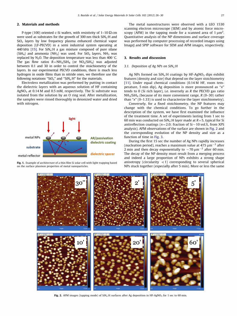
Fig. 2. AFM images (tapping mode) of SiNx:H surfaces a
The metal nanostructures were observed with a LEO 1530scanning electron microscope (SEM) and by atomic force micro-scopy (AFM) in the tapping mode for a scanned area of 1 mm2.Quantitative analysis of the NP dimensions and surface coveragewas performed by computer processing of recorded images usingImageJ and SPIP software for SEM and AFM images, respectively.
3. Results and discussion
3.1. Deposition of Ag NPs on SiNx:H
Ag NPs formed on SiNx:H coatings by HF-AgNO3 dips exhibitfeatures (density and size) that depend on the layer stoichiometry[11]. Under equal chemical conditions (0.14 M HF, room tem-perature, 5 min dip), Ag deposition is more pronounced as ‘‘x’’tends to 0 (Si rich layer), i.e. inversely as R the PECVD gas ratioNH3/SiH4 (because of its more convenient range, R (0–30) ratherthan ‘‘x’’ (0–1.33) is used to characterize the layer stoichiometry).
Conversely, for a fixed stoichiometry, the NP features maychange with the chemical conditions. To go further in thedescription of the system, we have first examined the influenceof the treatment time. A set of experiments lasting from 1 sec to60 min was conducted on SiNx:H layer made at R¼5, typical for Siantireflection coatings (n¼2.0; fraction of Si�10 vol.%, from XPSanalysis). AFM observations of the surface are shown in Fig. 2 andthe corresponding evolution of the NP density and size as afunction of time in Fig. 3.
During the first 15 sec the number of Ag NPs rapidly increases(nucleation period), reaches a maximum value at 475 mm�2 after2 min and then decay exponentially to �70 mm�2 after 60 min.The decay of the NP density must result from a merging processand indeed a large proportion of NPs exhibits a strong shapeanisotropy (circularity 51) corresponding to several sphericalNPs stuck together (especially after 5 min). More or less the same
fter Ag deposition in HF-AgNO3 for 1 sec to 60 min.

Fig. 3. Size and density of Au NPs as a function of deposition time.
Fig. 4. Maximum NP density as a function of R, taken from plots of the NP density
with time as shown in the inset for R¼1, 3, 7 and 30.
Fig. 5. Total volume of Ag deposited by mm2 as a function of the temperature (HF
0.14 M, 5 min).
S. Bastide et al. / Solar Energy Materials & Solar Cells 102 (2012) 26–3028
evolution is followed for samples with other stoichiometries (seeR¼1, 3, 7 and 30 in the inset of Fig. 4), with a maximum densityreached after �2 min. As shown in Fig. 4, the maximum densitychanges by almost three orders of magnitude depending on R.
The NP size increases almost linearly with time (Fig. 3, rightaxis) to reach a mean value of �100 nm after 60 min. Note thatthis size represents the ‘‘sphere equivalent diameter’’ calculatedfrom the NP volume (taking into account the coverage, the NPmean height and density). If we consider the total volume ofdeposited Ag as a function of time, it increases linearly with timeas well (not shown here). This is rather surprising if we supposethat Ag deposition relies on the Si nanoclusters in contact withthe electrolyte, i.e. those at the very surface of the layer. However,it is well known that HF dissolves SiNx:H [16] and as a conse-quence the Si nanoclusters embedded in the layer are progres-sively uncovered (‘‘iceberg effect’’) [11]. When brought in contactwith the electrolyte, new Ag nanoclusters are formed thataggregate with already existing NPs. Hence, the process can beviewed as a constant supply of Ag accompanied with a merging ofNPs, both factors contributing to an increase in NP size with time.
Results from the metallization of SiNx:H layers (R¼5; 5 min) atdifferent bath temperatures support this interpretation. As shownin Fig. 5, the total volume of deposited Ag per mm2 clearlyincreases with the temperature (5 min treatment). Obviouslychanging the temperature must affect the dissolution rate ofSiNx:H and therefore the volume of Si made available for Ag
deposition. Measurements of the etch rate of SiNx:H in 0.14 M HFat 15, 25 and 35 1C give 0.9, 1.7 and 2.8 nm/min, respectively.Changing the bath temperature from 15 to 35 1C leads to anincrease in etch rate by a factor of 3.1. The volume ratio ofdeposited Ag found experimentally is 2.7, in relatively goodagreement with the latter.
3.2. Electroless deposition of Ag NPs on SiOx layers
SiOx is another Si based dielectric commonly used in photo-voltaics as an antireflection coatings (often in double or triplestacks with SiNx) [17] and for surface passivation [18,19]. ThePECVD process is based on the use of SiH4 and N2O as precursorgases and the stoichiometry can also be adjusted by controllingthe gas ratio R to form Si rich SiOx (low R) to stoichiometric SiO2
(R¼30). A Si phase is also found in the form of c-Si nanoclusters,and its fraction is inversely proportional to the value of R [20].Because of these similarities with SiNx:H, the electroless platingdescribed here should work for SiOx as well. Ag deposition wascarried out in the same chemical conditions, i.e. 0.14 M HF,0.5 mM AgNO3 and 5 min dip at room temperature. Fig. 6 showstopographical SEM views of the Ag nanostructures obtained onSiOx as a function of the stoichiometric ratio R.
The general trends are similar to those for SiNx:H: (i) welldefined individual Ag nanoparticles are obtained; (ii) the surfacecoverage decreases inversely as R, i.e. when the layer becomes Sipoor. However, there are also significant differences. Up to R¼10,the surface coverage seems to be identical for all stoichiometriesand a bimodal distribution of size is observed with maxima at 40and 10 nm. At R¼30, the surface coverage is much lower and onlysmall NPs are observed, with a mean diameter of 20 nm. Hence,for SiOx layers the stoichiometry induced tuning of Ag NP size anddensity occurs in a much narrower range of R. What we observeindirectly via Ag deposition should correspond to a strong varia-tion in stoichiometry in this range but the reason for this is notclear yet and a detailed investigation of the electroless plating ofSiOx for R values between 10 and 30 has been undertaken.
3.3. Application in a solar cell process
Integration of the electroless Ag deposition in a solar cellprocess can be foreseen practically. Taking advantage of thePECVD step, the SiNx:H antireflection coating/passivating layercould be stacked with a top sacrificial layer serving to form AgNPs during a subsequent HF-AgNO3 dip. The NP density and size
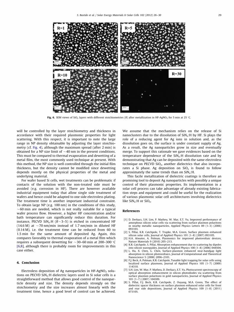
Fig. 6. SEM views of SiOx layers with different stoichiometries (R) after metallization in HF-AgNO3 for 5 min at 25 1C.
S. Bastide et al. / Solar Energy Materials & Solar Cells 102 (2012) 26–30 29
will be controlled by the layer stoichiometry and thickness inaccordance with their required plasmonic properties for lightscattering. With this respect, it is important to note the largerange in NP density obtainable by adjusting the layer stoichio-metry (cf. Fig. 4), although the maximum spread (after 2 min) isobtained for a NP size limit of �40 nm in the present conditions.This must be compared to thermal evaporation and dewetting of ametal film, the most commonly used technique at present. Withthis method, the NP size is well controlled through the initial filmthickness, but the density cannot be modified since dewettingdepends mostly on the physical properties of the metal andunderlying material.
For wafer based Si cells, wet treatments can be problematic ifcontacts of the solution with the non-treated side must beavoided (e.g. corrosion in HF). There are however availableindustrial equipment today that allow single side treatment ofwafers and hence could be adapted to one side electroless plating.The treatment time is another important industrial constraint.To obtain large NP (e.g. 100 nm) in the conditions of this study,�60 min are needed, which is not really suitable for a typicalwafer process flow. However, a higher HF concentration and/orbath temperature can significantly reduce this duration. Forinstance, PECVD SiNx:H (R�3–5) is etched in concentrated HF(14.6 M) at �70 nm/min instead of 1.7 nm/min in diluted HF(0.14 M), i.e. the treatment time can be reduced from 60 to1.5 min for the same amount of deposited Ag. Again, thiscompares favorably to thermal evaporation of a metal film whichrequires a subsequent dewetting for �30–60 min at 200–300 1C[6,8], although there is probably room for improvements in thiscase either.
4. Conclusion
Electroless deposition of Ag nanoparticles in HF-AgNO3 solu-tions on PECVD SiNx:H dielectric layers used in Si solar cells is astraightforward method that allows good control of the nanopar-ticle density and size. The density depends strongly on thestoichiometry and the size increases almost linearly with thetreatment time, hence a good level of control can be achieved.
We assume that the mechanism relies on the release of Sinanoclusters due to the dissolution of SiNx:H by HF. Si plays therole of a reducing agent for Ag ions in solution and, as thedissolution goes on, the surface is under constant supply of Ag.As a result, the Ag nanoparticles grow in size and eventuallymerge. To support this rationale we gave evidences based on thetemperature dependence of the SiNx:H dissolution rate and bydemonstrating that Ag can be deposited with the same electrolesstechnique on PECVD SiOx, another dielectrics that also incorpo-rates a Si phase. Ag deposition on SiOx is found to followapproximately the same trends than on SiNx:H.
This facile metallization of dielectric coatings is therefore anpromising tool to deposit Ag nanoparticles with possibly a uniquecontrol of their plasmonic properties. Its implementation in asolar cell process can take advantage of already existing fabrica-tion steps and equipment and could be useful for the realizationof various plasmonic solar cell architectures involving dielectricslike SiNx:H or SiOx.
References
[1] D. Derkacs, S.H. Lim, P. Matheu, W. Mar, E.T. Yu, Improved performance ofamorphous silicon solar cells via scattering from surface plasmon polaritonsin nearby metallic nanoparticles, Applied Physics Letters 89 (1–3) (2006)093103.
[2] S. Pillai, K.R. Catchpole, T. Trupke, M.A. Green, Surface plasmon enhancedsilicon solar cells, Journal of Applied Physics 101 (1–8) (2007) 093105.
[3] H.A. Atwater, A. Polman, Plasmonics for improved photovoltaic devices,Nature Materials 9 (2010) 205–213.
[4] K.R. Catchpole, S. Pillai, Absorption enhancement due to scattering by dipolesinto silicon waveguides, Journal of Applied Physics 100 (1–8) (2006) 044504.
[5] L. Hu, X. Chen, G. Chen, Surface-plasmon enhanced near-bandgap lightabsorption in silicon photovoltaics, Journal of Computational and TheoreticalNanoscience 5 (2008) 2096–2101.
[6] F.J. Beck, A. Polman, K.R. Catchpole, Tunable light trapping for solar cells usinglocalized surface plasmons, Journal of Applied Physics 105 (1–7) (2009)114310.
[7] S.H. Lim, W. Mar, P. Matheu, D. Derkacs, E.T. Yu, Photocurrent spectroscopy ofoptical absorption enhancement in silicon photodiodes via scattering fromsurface plasmon polaritons in gold nanoparticles, Journal of Applied Physics101 (1–7) (2007) 104309.
[8] S. Pillai, F.J. Beck, K.R. Catchpole, Z. Ouyang, M.A. Green, The effect ofdielectric spacer thickness on surface plasmon enhanced solar cells for frontand rear side depositions, Journal of Applied Physics 109 (1–8) (2011)073105.

S. Bastide et al. / Solar Energy Materials & Solar Cells 102 (2012) 26–3030
[9] F.J. Beck, S. Mokkapati, K.R. Catchpole, Plasmonic light-trapping for Si solarcells using self-assembled, Ag nanoparticles, Progress in Photovoltaics:Research and Applications 18 (2010) 500–504.
[10] R. Gupta, M.J. Dyer, W.A. Weimer, Preparation and characterization of surfaceplasmon resonance tunable gold and silver films, Journal of Applied Physics92 (1–8) (2002) 5264.
[11] T. Nychyporuk, Z. Zhan, A. Fave, M. Lemiti, S. Bastide, Electroless deposition ofAg nanoparticles on the surface of SiNx:H dielectric layers, Solar EnergyMaterials and Solar Cells 94 (12) (2010) 2314–2317.
[12] V. Lehmann, Electrochemistry of Silicon, Wiley-VCH, 2002, p. 58.[13] Z. Huang, N. Geyer, P. Werner, J. de Boor, U. Gosele, Metal-assisted chemical
etching of silicon: a review, Advanced Materials 23 (2011) 285–308.[14] K.-Q. Peng, Y.-J. Yan, S.-P. Gao, J. Zhu, Synthesis of large-area silicon
nanowires arrays via self-assembling nanoelectrochemistry, Advanced Mate-rials 14 (2002) 1164–1167.
[15] J.F. Lelievre, E. Fourmond, A. Kaminski, O. Palais, D. Ballutaud, M. Lemiti,Study of the composition of hydrogenated silicon nitride SiNx:H for efficient
surface and bulk passivation of silicon, Solar Energy Materials and Solar Cells93 (2009) 1281–1289.
[16] W. Kern, G.L. Schnable, in: S.J. Moss, A. Ledwith (Eds.), Chemistry of thesemiconductor industry, Blackie and Son Ltd, Glasgow, 1987, p. 252.
[17] Z. Chen, P. Sana, J. Salami, A. Rohatgi, A novel and effective PECVD SiO2/SiNantireflection coating for Si solar cells, IEEE Transactions on Electron Devices40 (1993) 1161–1165.
[18] Z. Chen, A. Rohatgi, R.O. Bell, J.P. Kalejs, Defect passivation in multicrystal-line-Si materials by plasma enhanced chemical vapor deposition of SiO2/SiNcoatings, Applied Physics Letters 65 (1994) 2078–2080.
[19] M. Hofmann, S. Kambor, C. Schmidt, D. Grambole, J. Rentsch, S.W. Glunz,R. Preu, PECVD-ONO: a new deposited firing stable rear surface passivationlayer system for crystalline silicon solar cells, Advances in Opto Electronics2008 (1-10) Article ID 485467, doi:10.1155/2008/485467.
[20] M. Bedjaoui, B. Despax, M. Caumont, C. Bonafos, Si nanocrystal-containingSiOx (xo2) produced by thermal annealing of PECVD realized thin films,Materials Science and Engineering: B 124 (2005) 508–512.