snvs746e – march 2000– revised may 2013 lm134/lm234/lm334 … · · 2017-04-27lm134, lm234,...
TRANSCRIPT

LM134, LM234, LM334
www.ti.com SNVS746E –MARCH 2000–REVISED MAY 2013
LM134/LM234/LM334 3-Terminal Adjustable Current SourcesCheck for Samples: LM134, LM234, LM334
1FEATURESThe sense voltage used to establish operating current
2• Operates From 1V to 40Vin the LM134 is 64mV at 25°C and is directly• 0.02%/V Current Regulationproportional to absolute temperature (°K). The
• Programmable From 1μA to 10mA simplest one external resistor connection, then,generates a current with ≈+0.33%/°C temperature• True 2-Terminal Operationdependence. Zero drift operation can be obtained by• Available as Fully Specified Temperatureadding one extra resistor and a diode.SensorApplications for the current sources include bias• ±3% Initial Accuracynetworks, surge protection, low power reference,ramp generation, LED driver, and temperatureDESCRIPTIONsensing. The LM234-3 and LM234-6 are specified as
The LM134/LM234/LM334 are 3-terminal adjustable true temperature sensors with ensured initialcurrent sources featuring 10,000:1 range in operating accuracy of ±3°C and ±6°C, respectively. Thesecurrent, excellent current regulation and a wide devices are ideal in remote sense applicationsdynamic voltage range of 1V to 40V. Current is because series resistance in long wire runs does notestablished with one external resistor and no other affect accuracy. In addition, only 2 wires are required.parts are required. Initial current accuracy is ±3%.
The LM134 is specified over a temperature range ofThe LM134/LM234/LM334 are true floating current−55°C to +125°C, the LM234 from −25°C to +100°Csources with no separate power supply connections.and the LM334 from 0°C to +70°C. These devicesIn addition, reverse applied voltages of up to 20V willare available in TO hermetic, TO-92 and SOIC-8draw only a few dozen microamperes of current,plastic packages.allowing the devices to act as both a rectifier and
current source in AC applications.
Connection Diagrams
Figure 1. SOIC-8 Surface Mount Package Figure 2. SOIC-8 Alternative Pinout Surface MountPackage(LM334M; LM334M/NOPB; LM334MX;
LM334MX/NOPB) (LM334SM; LM334SM/NOPB; LM334SMX;LM334SMX/NOPB)See Package Number D
See Package Number D
Figure 3. TO Metal Can Package (Bottom View) Figure 4. TO-92 Plastic Package (Bottom View)See Package Number NDV See Package Number LP
1
Please be aware that an important notice concerning availability, standard warranty, and use in critical applications ofTexas Instruments semiconductor products and disclaimers thereto appears at the end of this data sheet.
2All trademarks are the property of their respective owners.
PRODUCTION DATA information is current as of publication date. Copyright © 2000–2013, Texas Instruments IncorporatedProducts conform to specifications per the terms of the TexasInstruments standard warranty. Production processing does notnecessarily include testing of all parameters.

LM134, LM234, LM334
SNVS746E –MARCH 2000–REVISED MAY 2013 www.ti.com
These devices have limited built-in ESD protection. The leads should be shorted together or the device placed in conductive foamduring storage or handling to prevent electrostatic damage to the MOS gates.
Absolute Maximum Ratings (1) (2)
V+ to V− Forward Voltage LM134/LM234/LM334 40V
LM234-3/LM234-6 30V
V+ to V− Reverse Voltage 20V
R Pin to V− Voltage 5V
Set Current 10 mA
Power Dissipation 400 mW
ESD Susceptibility (3) 2000V
Operating Temperature Range (4) LM134 −55°C to +125°C
LM234/LM234-3/LM234-6 −25°C to +100°C
LM334 0°C to +70°C
Soldering Information TO-92 Package (10 sec.) 260°C
TO Package (10 sec.) 300°C
SOIC Package Vapor Phase (60 sec.) 215°C
Infrared (15 sec.) 220°C
(1) “Absolute Maximum Ratings” indicate limits beyond which damage to the device may occur. Operating Ratings indicate conditions forwhich the device is functional, but do not ensure specific performance limits.
(2) If Military/Aerospace specified devices are required, please contact the Texas Instruments Sales Office/Distributors for availability andspecifications.
(3) Human body model, 100pF discharged through a 1.5kΩ resistor.(4) For elevated temperature operation, TJ max is:
LM134 150°C
LM234 125°C
LM334 100°C
See Thermal Characteristics.
Thermal Characteristicsover operating free-air temperature range (unless otherwise noted)
Thermal Resistance TO-92 TO SOIC-8
θja (Junction to Ambient) 180°C/W (0.4″ leads) 440°C/W 165°C/W
160°C/W (0.125″ leads)
θjc (Junction to Case) N/A 32°C/W 80°C/W
2 Submit Documentation Feedback Copyright © 2000–2013, Texas Instruments Incorporated
Product Folder Links: LM134 LM234 LM334

LM134, LM234, LM334
www.ti.com SNVS746E –MARCH 2000–REVISED MAY 2013
Electrical Characteristics (1)
LM134/LM234 LM334Parameter Conditions Units
Min Typ Max Min Typ Max
Set Current Error, V+=2.5V (2) 10μA ≤ ISET ≤ 1mA 3 6 %
1mA < ISET ≤ 5mA 5 8 %
2μA ≤ ISET < 10μA 8 12 %
Ratio of Set Current to Bias 100μA ≤ ISET ≤ 1mA 14 18 23 14 18 26Current 1mA ≤ ISET ≤ 5mA 14 14
2 μA≤ISET≤100 μA 18 23 18 26
Minimum Operating Voltage 2μA ≤ ISET ≤ 100μA 0.8 0.8 V
100μA < ISET ≤ 1mA 0.9 0.9 V
1mA < ISET ≤ 5mA 1.0 1.0 V
Average Change in Set Current 2μA ≤ ISET ≤ 1mA 1.5 ≤ V+ ≤ 5V 0.02 0.05 0.02 0.1 %/Vwith Input Voltage 5V ≤ V+ ≤ 40V 0.01 0.03 0.01 0.05 %/V
1mA < ISET ≤ 5mA 1.5V ≤ V ≤ 5V 0.03 0.03 %/V
5V ≤ V ≤ 40V 0.02 0.02 %/V
Temperature Dependence of 25μA ≤ ISET ≤ 1mA 0.96T T 1.04T 0.96T T 1.04TSet Current (3)
Effective Shunt Capacitance 15 15 pF
(1) Unless otherwise specified, tests are performed at Tj = 25°C with pulse testing so that junction temperature does not change during test(2) Set current is the current flowing into the V+ pin. For the Basic 2-Terminal Current Source circuit shown in Figure 13. ISET is determined
by the following formula: ISET = 67.7 mV/RSET (@ 25°C). Set current error is expressed as a percent deviation from this amount. ISETincreases at 0.336%/°C @ Tj = 25°C (227 μV/°C).
(3) ISET is directly proportional to absolute temperature (°K). ISET at any temperature can be calculated from: ISET = Io (T/To) where Io is ISETmeasured at To (°K).
Electrical Characteristics (1)
LM234-3 LM234-6Parameter Conditions Units
Min Typ Max Min Typ Max
Set Current Error, V+=2.5V (2) 100μA ≤ ISET ≤ 1mA ±1 ±2 %
TJ = 25°
Equivalent Temperature Error ±3 ±6 °C
Ratio of Set Current to Bias 100μA ≤ ISET ≤ 1mA 14 18 26 14 18 26Current
Minimum Operating Voltage 100μA ISET ≤ 1mA 0.9 0.9 V
Average Change in Set Current 100μA ≤ ISET ≤ 1mA 1.5 ≤ V+ ≤ 5V 0.02 0.05 0.02 0.01 %/Vwith Input Voltage 5V ≤ V+ ≤ 30V 0.01 0.03 0.01 0.05 %/V
Temperature Dependence of 100μA ≤ ISET ≤ 1mA 0.98T T 1.02T 0.97T T 1.03TSet Current (3)
Equivalent Slope Error ±2 ±3 %
Effective Shunt Capacitance 15 15 pF
(1) Unless otherwise specified, tests are performed at Tj = 25°C with pulse testing so that junction temperature does not change during test(2) Set current is the current flowing into the V+ pin. For the Basic 2-Terminal Current Source circuit shown in Figure 13. ISET is determined
by the following formula: ISET = 67.7 mV/RSET (@ 25°C). Set current error is expressed as a percent deviation from this amount. ISETincreases at 0.336%/°C @ Tj = 25°C (227 μV/°C).
(3) ISET is directly proportional to absolute temperature (°K). ISET at any temperature can be calculated from: ISET = Io (T/To) where Io is ISETmeasured at To (°K).
Copyright © 2000–2013, Texas Instruments Incorporated Submit Documentation Feedback 3
Product Folder Links: LM134 LM234 LM334

LM134, LM234, LM334
SNVS746E –MARCH 2000–REVISED MAY 2013 www.ti.com
Typical Performance Characteristics
Maximum Slew RateOutput Impedance Linear Operation
Figure 5. Figure 6.
Start-Up Transient Response
Figure 7. Figure 8.
Voltage Across RSET (VR) Current Noise
Figure 9. Figure 10.
4 Submit Documentation Feedback Copyright © 2000–2013, Texas Instruments Incorporated
Product Folder Links: LM134 LM234 LM334
LM134, LM234, LM334
www.ti.com SNVS746E –MARCH 2000–REVISED MAY 2013
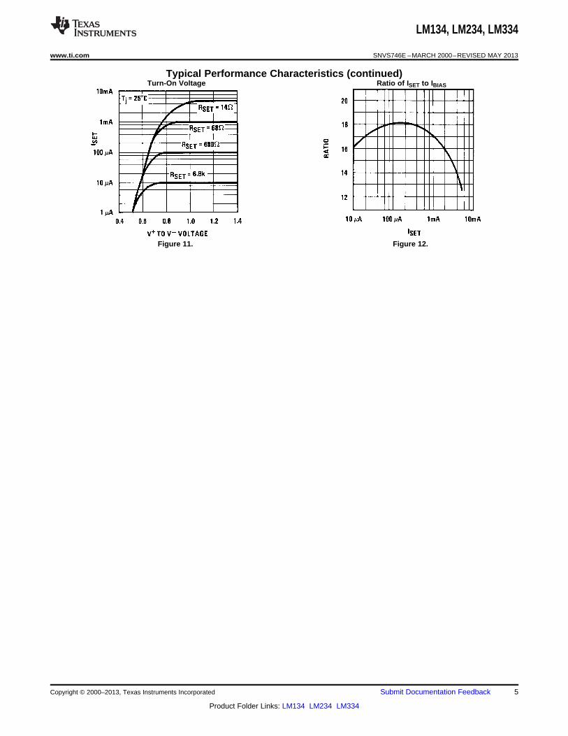
Typical Performance Characteristics (continued)Turn-On Voltage Ratio of ISET to IBIAS
Figure 11. Figure 12.
Copyright © 2000–2013, Texas Instruments Incorporated Submit Documentation Feedback 5
Product Folder Links: LM134 LM234 LM334

LM134, LM234, LM334
SNVS746E –MARCH 2000–REVISED MAY 2013 www.ti.com
APPLICATION HINTS
The LM134 has been designed for ease of application, but a general discussion of design features is presentedhere to familiarize the designer with device characteristics which may not be immediately obvious. These includethe effects of slewing, power dissipation, capacitance, noise, and contact resistance.
Calculating RSET
The total current through the LM134 (ISET) is the sum of the current going through the SET resistor (IR) and theLM134's bias current (IBIAS), as shown in Figure 13.
Figure 13. Basic Current Source
A graph showing the ratio of these two currents is supplied under Ratio of ISET to IBIAS in Typical PerformanceCharacteristics. The current flowing through RSET is determined by VR, which is approximately 214μV/°K (64mV/298°K ∼ 214μV/°K).
(1)
Since (for a given set current) IBIAS is simply a percentage of ISET, the equation can be rewritten
where• n is the ratio of ISET to IBIAS as specified in Electrical Characteristics and shown in the graph (2)
Since n is typically 18 for 2μA ≤ ISET ≤ 1mA, the equation can be further simplified to
(3)
for most set currents.
Slew Rate
At slew rates above a given threshold (see curve), the LM134 may exhibit non-linear current shifts. The slewingrate at which this occurs is directly proportional to ISET. At ISET = 10μA, maximum dV/dt is 0.01V/μs; at ISET =1mA, the limit is 1V/μs. Slew rates above the limit do not harm the LM134, or cause large currents to flow.
Thermal Effects
Internal heating can have a significant effect on current regulation for ISET greater than 100μA. For example, each1V increase across the LM134 at ISET = 1 mA will increase junction temperature by ≈0.4°C in still air. Outputcurrent (ISET) has a temperature coefficient of ≈0.33%/°C, so the change in current due to temperature rise will be(0.4) (0.33) = 0.132%. This is a 10:1 degradation in regulation compared to true electrical effects. Thermaleffects, therefore, must be taken into account when DC regulation is critical and ISET exceeds 100μA. Heatsinking of the TO package or the TO-92 leads can reduce this effect by more than 3:1.
6 Submit Documentation Feedback Copyright © 2000–2013, Texas Instruments Incorporated
Product Folder Links: LM134 LM234 LM334

LM134, LM234, LM334
www.ti.com SNVS746E –MARCH 2000–REVISED MAY 2013
Shunt Capacitance
In certain applications, the 15 pF shunt capacitance of the LM134 may have to be reduced, either because ofloading problems or because it limits the AC output impedance of the current source. This can be easilyaccomplished by buffering the LM134 with an FET as shown in the applications. This can reduce capacitance toless than 3 pF and improve regulation by at least an order of magnitude. DC characteristics (with the exceptionof minimum input voltage), are not affected.
Noise
Current noise generated by the LM134 is approximately 4 times the shot noise of a transistor. If the LM134 isused as an active load for a transistor amplifier, input referred noise will be increased by about 12dB. In manycases, this is acceptable and a single stage amplifier can be built with a voltage gain exceeding 2000.
Lead Resistance
The sense voltage which determines operating current of the LM134 is less than 100mV. At this level,thermocouple or lead resistance effects should be minimized by locating the current setting resistor physicallyclose to the device. Sockets should be avoided if possible. It takes only 0.7Ω contact resistance to reduce outputcurrent by 1% at the 1 mA level.
Sensing Temperature
The LM134 makes an ideal remote temperature sensor because its current mode operation does not loseaccuracy over long wire runs. Output current is directly proportional to absolute temperature in degrees Kelvin,according to the following formula:
(4)
Calibration of the LM134 is greatly simplified because of the fact that most of the initial inaccuracy is due to again term (slope error) and not an offset. This means that a calibration consisting of a gain adjustment only willtrim both slope and zero at the same time. In addition, gain adjustment is a one point trim because the output ofthe LM134 extrapolates to zero at 0°K, independent of RSET or any initial inaccuracy.
Figure 14. Gain Adjustment
This property of the LM134 is illustrated in the accompanying graph. Line abc is the sensor current beforetrimming. Line a′b′c′ is the desired output. A gain trim done at T2 will move the output from b to b′ and willsimultaneously correct the slope so that the output at T1 and T3 will be correct. This gain trim can be done onRSET or on the load resistor used to terminate the LM134. Slope error after trim will normally be less than ±1%.To maintain this accuracy, however, a low temperature coefficient resistor must be used for RSET.
A 33 ppm/°C drift of RSET will give a 1% slope error because the resistor will normally see about the sametemperature variations as the LM134. Separating RSET from the LM134 requires 3 wires and has lead resistanceproblems, so is not normally recommended. Metal film resistors with less than 20 ppm/°C drift are readilyavailable. Wire wound resistors may also be used where best stability is required.
Copyright © 2000–2013, Texas Instruments Incorporated Submit Documentation Feedback 7
Product Folder Links: LM134 LM234 LM334

LM134, LM234, LM334
SNVS746E –MARCH 2000–REVISED MAY 2013 www.ti.com
Application as a Zero Temperature Coefficent Current Source
Adding a diode and a resistor to the standard LM134 configuration can cancel the temperature-dependentcharacteristic of the LM134. The circuit shown in Figure 15 balances the positive tempco of the LM134 (about+0.23 mV/°C) with the negative tempco of a forward-biased silicon diode (about −2.5 mV/°C).
Figure 15. Zero Tempco Current Source
The set current (ISET) is the sum of I1 and I2, each contributing approximately 50% of the set current, and IBIAS.IBIAS is usually included in the I1 term by increasing the VR value used for calculations by 5.9%. (SeeCALCULATING RSET.)
(5)
The first step is to minimize the tempco of the circuit, using the following equations. An example is given using avalue of +227μV/°C as the tempco of the LM134 (which includes the IBIAS component), and −2.5 mV/°C as thetempco of the diode (for best results, this value should be directly measured or obtained from the manufacturerof the diode).
(6)
(7)
With the R1 to R2 ratio determined, values for R1 and R2 should be determined to give the desired set current.The formula for calculating the set current at T = 25°C is shown below, followed by an example that assumes theforward voltage drop across the diode (VD) is 0.6V, the voltage across R1 is 67.7mV (64 mV + 5.9% to accountfor IBIAS), and R2/R1 = 10 (from the previous calculations).
8 Submit Documentation Feedback Copyright © 2000–2013, Texas Instruments Incorporated
Product Folder Links: LM134 LM234 LM334

LM134, LM234, LM334
www.ti.com SNVS746E –MARCH 2000–REVISED MAY 2013
(8)
This circuit will eliminate most of the LM134's temperature coefficient, and it does a good job even if theestimates of the diode's characteristics are not accurate (as the following example will show). For lowest tempcowith a specific diode at the desired ISET, however, the circuit should be built and tested over temperature. If themeasured tempco of ISET is positive, R2 should be reduced. If the resulting tempco is negative, R2 should beincreased. The recommended diode for use in this circuit is the 1N457 because its tempco is centered at 11times the tempco of the LM134, allowing R2 = 10 R1. You can also use this circuit to create a current source withnon-zero tempcos by setting the tempco component of the tempco equation to the desired value instead of 0.
EXAMPLE: A 1mA, Zero-Tempco Current Source
First, solve for R1 and R2:
(9)
The values of R1 and R2 can be changed to standard 1% resistor values (R1 = 133Ω and R2 = 1.33kΩ) with lessthan a 0.75% error.
If the forward voltage drop of the diode was 0.65V instead of the estimate of 0.6V (an error of 8%), the actual setcurrent will be
(10)
an error of less than 5%.
If the estimate for the tempco of the diode's forward voltage drop was off, the tempco cancellation is stillreasonably effective. Assume the tempco of the diode is 2.6mV/°C instead of 2.5mV/°C (an error of 4%). Thetempco of the circuit is now:
(11)
A 1mA LM134 current source with no temperature compensation would have a set resistor of 68Ω and aresulting tempco of
(12)
So even if the diode's tempco varies as much as ±4% from its estimated value, the circuit still eliminates 98% ofthe LM134's inherent tempco.
Copyright © 2000–2013, Texas Instruments Incorporated Submit Documentation Feedback 9
Product Folder Links: LM134 LM234 LM334

LM134, LM234, LM334
SNVS746E –MARCH 2000–REVISED MAY 2013 www.ti.com
Typical Applications
*Select R3 = VREF/583μA. VREF may be any stable positive voltage ≥ 2VTrim R3 to calibrate
Figure 16. Ground Referred Fahrenheit Thermometer
Figure 17. Terminating Remote Sensor for Voltage Output
*Output impedance of the LM134 at the “R” pin is approximately
where R2 is the equivalent external resistance connected from the V− pin to ground. This negative resistance can bereduced by a factor of 5 or more by inserting an equivalent resistor R3 = (R2/16) in series with the output.
Figure 18. Low Output Impedance Thermometer
10 Submit Documentation Feedback Copyright © 2000–2013, Texas Instruments Incorporated
Product Folder Links: LM134 LM234 LM334

LM134, LM234, LM334
www.ti.com SNVS746E –MARCH 2000–REVISED MAY 2013
Figure 19. Low Output Impedance Thermometer
*Select R1 and C1 for optimum stability
Figure 20. Higher Output Current
Figure 21. Basic 2-Terminal Current Source
Copyright © 2000–2013, Texas Instruments Incorporated Submit Documentation Feedback 11
Product Folder Links: LM134 LM234 LM334

LM134, LM234, LM334
SNVS746E –MARCH 2000–REVISED MAY 2013 www.ti.com
Figure 22. Micropower Bias
Figure 23. Low Input Voltage Reference Driver
Figure 24. Ramp Generator
12 Submit Documentation Feedback Copyright © 2000–2013, Texas Instruments Incorporated
Product Folder Links: LM134 LM234 LM334

LM134, LM234, LM334
www.ti.com SNVS746E –MARCH 2000–REVISED MAY 2013
*Select ratio of R1 to R2 to obtain zero temperature drift
Figure 25. 1.2V Reference Operates on 10 μA and 2V
*Select ratio of R1 to R2 for zero temperature drift
Figure 26. 1.2V Regulator with 1.8V Minimum Input
Figure 27. Zener Biasing
Copyright © 2000–2013, Texas Instruments Incorporated Submit Documentation Feedback 13
Product Folder Links: LM134 LM234 LM334

LM134, LM234, LM334
SNVS746E –MARCH 2000–REVISED MAY 2013 www.ti.com
*For ±10% adjustment, select RSET10% high, and make R1 ≈ 3 RSET
Figure 28. Alternate Trimming Technique
Figure 29. Buffer for Photoconductive Cell
*Select Q1 or Q2 to ensure at least 1V across the LM134. Vp (1 − ISET/IDSS) ≥ 1.2V.
14 Submit Documentation Feedback Copyright © 2000–2013, Texas Instruments Incorporated
Product Folder Links: LM134 LM234 LM334

LM134, LM234, LM334
www.ti.com SNVS746E –MARCH 2000–REVISED MAY 2013
Figure 30. FET Cascoding for Low Capacitance and/or Ultra High Output Impedance
*ZOUT ≈ −16 • R1 (R1/VIN must not exceed ISET)
Figure 31. Generating Negative Output Impedance
*Use minimum value required to ensure stability of protected device. This minimizes inrush current to a direct short.
Figure 32. In-Line Current Limiter
Copyright © 2000–2013, Texas Instruments Incorporated Submit Documentation Feedback 15
Product Folder Links: LM134 LM234 LM334

LM134, LM234, LM334
SNVS746E –MARCH 2000–REVISED MAY 2013 www.ti.com
Schematic Diagram
16 Submit Documentation Feedback Copyright © 2000–2013, Texas Instruments Incorporated
Product Folder Links: LM134 LM234 LM334

LM134, LM234, LM334
www.ti.com SNVS746E –MARCH 2000–REVISED MAY 2013
REVISION HISTORY
Changes from Revision C (April 2013) to Revision D Page
• Changed layout of National Data Sheet to TI format .......................................................................................................... 16
Copyright © 2000–2013, Texas Instruments Incorporated Submit Documentation Feedback 17
Product Folder Links: LM134 LM234 LM334

PACKAGE OPTION ADDENDUM
www.ti.com 27-Jul-2016
Addendum-Page 1
PACKAGING INFORMATION
Orderable Device Status(1)
Package Type PackageDrawing
Pins PackageQty
Eco Plan(2)
Lead/Ball Finish(6)
MSL Peak Temp(3)
Op Temp (°C) Device Marking(4/5)
Samples
LM134 MDC ACTIVE DIESALE Y 0 400 Green (RoHS& no Sb/Br)
Call TI Level-1-NA-UNLIM -40 to 85
LM134H ACTIVE TO NDV 3 1000 TBD Call TI Call TI -55 to 125 ( LM134H ~ LM134H)
LM134H/NOPB ACTIVE TO NDV 3 1000 Green (RoHS& no Sb/Br)
Call TI Level-1-NA-UNLIM -55 to 125 ( LM134H ~ LM134H)
LM234Z-3/NOPB ACTIVE TO-92 LP 3 1800 Green (RoHS& no Sb/Br)
CU SN N / A for Pkg Type -25 to 100 LM234Z-3
LM234Z-6/NOPB ACTIVE TO-92 LP 3 1800 Green (RoHS& no Sb/Br)
CU SN N / A for Pkg Type -25 to 100 LM234Z-6
LM334 MWC ACTIVE WAFERSALE YS 0 1 Green (RoHS& no Sb/Br)
Call TI Level-1-NA-UNLIM -40 to 85
LM334M NRND SOIC D 8 95 TBD Call TI Call TI 0 to 70 LM334M
LM334M/NOPB ACTIVE SOIC D 8 95 Green (RoHS& no Sb/Br)
CU SN Level-1-260C-UNLIM 0 to 70 LM334M
LM334MX/NOPB ACTIVE SOIC D 8 2500 Green (RoHS& no Sb/Br)
CU SN Level-1-260C-UNLIM 0 to 70 LM334M
LM334SM NRND SOIC D 8 95 TBD Call TI Call TI 0 to 70 LM334SM
LM334SM/NOPB ACTIVE SOIC D 8 95 Green (RoHS& no Sb/Br)
CU SN Level-1-260C-UNLIM 0 to 70 LM334SM
LM334SMX NRND SOIC D 8 2500 TBD Call TI Call TI 0 to 70 LM334SM
LM334SMX/NOPB ACTIVE SOIC D 8 2500 Green (RoHS& no Sb/Br)
CU SN Level-1-260C-UNLIM 0 to 70 LM334SM
LM334Z/LFT1 ACTIVE TO-92 LP 3 2000 Green (RoHS& no Sb/Br)
CU SN N / A for Pkg Type LM334Z
LM334Z/NOPB ACTIVE TO-92 LP 3 1800 Green (RoHS& no Sb/Br)
CU SN N / A for Pkg Type 0 to 70 LM334Z
(1) The marketing status values are defined as follows:ACTIVE: Product device recommended for new designs.LIFEBUY: TI has announced that the device will be discontinued, and a lifetime-buy period is in effect.NRND: Not recommended for new designs. Device is in production to support existing customers, but TI does not recommend using this part in a new design.PREVIEW: Device has been announced but is not in production. Samples may or may not be available.

PACKAGE OPTION ADDENDUM
www.ti.com 27-Jul-2016
Addendum-Page 2
OBSOLETE: TI has discontinued the production of the device.
(2) Eco Plan - The planned eco-friendly classification: Pb-Free (RoHS), Pb-Free (RoHS Exempt), or Green (RoHS & no Sb/Br) - please check http://www.ti.com/productcontent for the latest availabilityinformation and additional product content details.TBD: The Pb-Free/Green conversion plan has not been defined.Pb-Free (RoHS): TI's terms "Lead-Free" or "Pb-Free" mean semiconductor products that are compatible with the current RoHS requirements for all 6 substances, including the requirement thatlead not exceed 0.1% by weight in homogeneous materials. Where designed to be soldered at high temperatures, TI Pb-Free products are suitable for use in specified lead-free processes.Pb-Free (RoHS Exempt): This component has a RoHS exemption for either 1) lead-based flip-chip solder bumps used between the die and package, or 2) lead-based die adhesive used betweenthe die and leadframe. The component is otherwise considered Pb-Free (RoHS compatible) as defined above.Green (RoHS & no Sb/Br): TI defines "Green" to mean Pb-Free (RoHS compatible), and free of Bromine (Br) and Antimony (Sb) based flame retardants (Br or Sb do not exceed 0.1% by weightin homogeneous material)
(3) MSL, Peak Temp. - The Moisture Sensitivity Level rating according to the JEDEC industry standard classifications, and peak solder temperature.
(4) There may be additional marking, which relates to the logo, the lot trace code information, or the environmental category on the device.
(5) Multiple Device Markings will be inside parentheses. Only one Device Marking contained in parentheses and separated by a "~" will appear on a device. If a line is indented then it is a continuationof the previous line and the two combined represent the entire Device Marking for that device.
(6) Lead/Ball Finish - Orderable Devices may have multiple material finish options. Finish options are separated by a vertical ruled line. Lead/Ball Finish values may wrap to two lines if the finishvalue exceeds the maximum column width.
Important Information and Disclaimer:The information provided on this page represents TI's knowledge and belief as of the date that it is provided. TI bases its knowledge and belief on informationprovided by third parties, and makes no representation or warranty as to the accuracy of such information. Efforts are underway to better integrate information from third parties. TI has taken andcontinues to take reasonable steps to provide representative and accurate information but may not have conducted destructive testing or chemical analysis on incoming materials and chemicals.TI and TI suppliers consider certain information to be proprietary, and thus CAS numbers and other limited information may not be available for release.
In no event shall TI's liability arising out of such information exceed the total purchase price of the TI part(s) at issue in this document sold by TI to Customer on an annual basis.

TAPE AND REEL INFORMATION
*All dimensions are nominal
Device PackageType
PackageDrawing
Pins SPQ ReelDiameter
(mm)
ReelWidth
W1 (mm)
A0(mm)
B0(mm)
K0(mm)
P1(mm)
W(mm)
Pin1Quadrant
LM334MX/NOPB SOIC D 8 2500 330.0 12.4 6.5 5.4 2.0 8.0 12.0 Q1
LM334SMX SOIC D 8 2500 330.0 12.4 6.5 5.4 2.0 8.0 12.0 Q1
LM334SMX/NOPB SOIC D 8 2500 330.0 12.4 6.5 5.4 2.0 8.0 12.0 Q1
PACKAGE MATERIALS INFORMATION
www.ti.com 5-Dec-2014
Pack Materials-Page 1

*All dimensions are nominal
Device Package Type Package Drawing Pins SPQ Length (mm) Width (mm) Height (mm)
LM334MX/NOPB SOIC D 8 2500 367.0 367.0 35.0
LM334SMX SOIC D 8 2500 367.0 367.0 35.0
LM334SMX/NOPB SOIC D 8 2500 367.0 367.0 35.0
PACKAGE MATERIALS INFORMATION
www.ti.com 5-Dec-2014
Pack Materials-Page 2

www.ti.com
PACKAGE OUTLINE
( 2.54)1.160.92
4.954.55
0.76 MAX 2.67 MAX
0.64 MAXUNCONTROLLEDLEAD DIA
3X12.7 MIN
3X 0.4830.407
-5.565.32
1.220.72
45
TO-CAN - 2.67 mm max heightNDV0003HTO-46
4219876/A 01/2017
NOTES: 1. All linear dimensions are in millimeters. Any dimensions in parenthesis are for reference only. Dimensioning and tolerancing per ASME Y14.5M.2. This drawing is subject to change without notice.3. Reference JEDEC registration TO-46.
1
2
3
SCALE 1.250

www.ti.com
EXAMPLE BOARD LAYOUT
0.07 MAXALL AROUND
0.07 MAXTYP
( 1.2)METAL
2X ( 1.2) METAL
3X ( 0.7) VIA
(R0.05) TYP
(2.54)
(1.27)
TO-CAN - 2.67 mm max heightNDV0003HTO-46
4219876/A 01/2017
LAND PATTERN EXAMPLENON-SOLDER MASK DEFINED
SCALE:12X
2XSOLDER MASKOPENING
SOLDER MASKOPENING
1
2
3


www.ti.com
PACKAGE OUTLINE
3X 2.672.03
5.214.44
5.344.32
3X12.7 MIN
2X 1.27 0.13
3X 0.550.38
4.193.17
3.43 MIN
3X 0.430.35
(2.54)NOTE 3
2X2.6 0.2
2X4 MAX
SEATINGPLANE
6X0.076 MAX
(0.51) TYP
(1.5) TYP
TO-92 - 5.34 mm max heightLP0003ATO-92
4215214/B 04/2017
NOTES: 1. All linear dimensions are in millimeters. Any dimensions in parenthesis are for reference only. Dimensioning and tolerancing per ASME Y14.5M.2. This drawing is subject to change without notice.3. Lead dimensions are not controlled within this area.4. Reference JEDEC TO-226, variation AA.5. Shipping method: a. Straight lead option available in bulk pack only. b. Formed lead option available in tape and reel or ammo pack. c. Specific products can be offered in limited combinations of shipping medium and lead options. d. Consult product folder for more information on available options.
EJECTOR PINOPTIONAL
PLANESEATING
STRAIGHT LEAD OPTION
3 2 1
SCALE 1.200
FORMED LEAD OPTIONOTHER DIMENSIONS IDENTICAL
TO STRAIGHT LEAD OPTION
SCALE 1.200

www.ti.com
EXAMPLE BOARD LAYOUT
0.05 MAXALL AROUND
TYP
(1.07)
(1.5) 2X (1.5)
2X (1.07)(1.27)
(2.54)
FULL RTYP
( 1.4)0.05 MAXALL AROUND
TYP
(2.6)
(5.2)
(R0.05) TYP
3X ( 0.9) HOLE
2X ( 1.4)METAL
3X ( 0.85) HOLE
(R0.05) TYP
4215214/B 04/2017
TO-92 - 5.34 mm max heightLP0003ATO-92
LAND PATTERN EXAMPLEFORMED LEAD OPTIONNON-SOLDER MASK DEFINED
SCALE:15X
SOLDER MASKOPENING
METAL
2XSOLDER MASKOPENING
1 2 3
LAND PATTERN EXAMPLESTRAIGHT LEAD OPTIONNON-SOLDER MASK DEFINED
SCALE:15X
METALTYP
SOLDER MASKOPENING
2XSOLDER MASKOPENING
2XMETAL
1 2 3

www.ti.com
TAPE SPECIFICATIONS
19.017.5
13.711.7
11.08.5
0.5 MIN
TYP-4.33.7
9.758.50
TYP2.92.4
6.755.95
13.012.4
(2.5) TYP
16.515.5
3223
4215214/B 04/2017
TO-92 - 5.34 mm max heightLP0003ATO-92
FOR FORMED LEAD OPTION PACKAGE
IMPORTANT NOTICE
Texas Instruments Incorporated (TI) reserves the right to make corrections, enhancements, improvements and other changes to itssemiconductor products and services per JESD46, latest issue, and to discontinue any product or service per JESD48, latest issue. Buyersshould obtain the latest relevant information before placing orders and should verify that such information is current and complete.TI’s published terms of sale for semiconductor products (http://www.ti.com/sc/docs/stdterms.htm) apply to the sale of packaged integratedcircuit products that TI has qualified and released to market. Additional terms may apply to the use or sale of other types of TI products andservices.Reproduction of significant portions of TI information in TI data sheets is permissible only if reproduction is without alteration and isaccompanied by all associated warranties, conditions, limitations, and notices. TI is not responsible or liable for such reproduceddocumentation. Information of third parties may be subject to additional restrictions. Resale of TI products or services with statementsdifferent from or beyond the parameters stated by TI for that product or service voids all express and any implied warranties for theassociated TI product or service and is an unfair and deceptive business practice. TI is not responsible or liable for any such statements.Buyers and others who are developing systems that incorporate TI products (collectively, “Designers”) understand and agree that Designersremain responsible for using their independent analysis, evaluation and judgment in designing their applications and that Designers havefull and exclusive responsibility to assure the safety of Designers' applications and compliance of their applications (and of all TI productsused in or for Designers’ applications) with all applicable regulations, laws and other applicable requirements. Designer represents that, withrespect to their applications, Designer has all the necessary expertise to create and implement safeguards that (1) anticipate dangerousconsequences of failures, (2) monitor failures and their consequences, and (3) lessen the likelihood of failures that might cause harm andtake appropriate actions. Designer agrees that prior to using or distributing any applications that include TI products, Designer willthoroughly test such applications and the functionality of such TI products as used in such applications.TI’s provision of technical, application or other design advice, quality characterization, reliability data or other services or information,including, but not limited to, reference designs and materials relating to evaluation modules, (collectively, “TI Resources”) are intended toassist designers who are developing applications that incorporate TI products; by downloading, accessing or using TI Resources in anyway, Designer (individually or, if Designer is acting on behalf of a company, Designer’s company) agrees to use any particular TI Resourcesolely for this purpose and subject to the terms of this Notice.TI’s provision of TI Resources does not expand or otherwise alter TI’s applicable published warranties or warranty disclaimers for TIproducts, and no additional obligations or liabilities arise from TI providing such TI Resources. TI reserves the right to make corrections,enhancements, improvements and other changes to its TI Resources. TI has not conducted any testing other than that specificallydescribed in the published documentation for a particular TI Resource.Designer is authorized to use, copy and modify any individual TI Resource only in connection with the development of applications thatinclude the TI product(s) identified in such TI Resource. NO OTHER LICENSE, EXPRESS OR IMPLIED, BY ESTOPPEL OR OTHERWISETO ANY OTHER TI INTELLECTUAL PROPERTY RIGHT, AND NO LICENSE TO ANY TECHNOLOGY OR INTELLECTUAL PROPERTYRIGHT OF TI OR ANY THIRD PARTY IS GRANTED HEREIN, including but not limited to any patent right, copyright, mask work right, orother intellectual property right relating to any combination, machine, or process in which TI products or services are used. Informationregarding or referencing third-party products or services does not constitute a license to use such products or services, or a warranty orendorsement thereof. Use of TI Resources may require a license from a third party under the patents or other intellectual property of thethird party, or a license from TI under the patents or other intellectual property of TI.TI RESOURCES ARE PROVIDED “AS IS” AND WITH ALL FAULTS. TI DISCLAIMS ALL OTHER WARRANTIES ORREPRESENTATIONS, EXPRESS OR IMPLIED, REGARDING RESOURCES OR USE THEREOF, INCLUDING BUT NOT LIMITED TOACCURACY OR COMPLETENESS, TITLE, ANY EPIDEMIC FAILURE WARRANTY AND ANY IMPLIED WARRANTIES OFMERCHANTABILITY, FITNESS FOR A PARTICULAR PURPOSE, AND NON-INFRINGEMENT OF ANY THIRD PARTY INTELLECTUALPROPERTY RIGHTS. TI SHALL NOT BE LIABLE FOR AND SHALL NOT DEFEND OR INDEMNIFY DESIGNER AGAINST ANY CLAIM,INCLUDING BUT NOT LIMITED TO ANY INFRINGEMENT CLAIM THAT RELATES TO OR IS BASED ON ANY COMBINATION OFPRODUCTS EVEN IF DESCRIBED IN TI RESOURCES OR OTHERWISE. IN NO EVENT SHALL TI BE LIABLE FOR ANY ACTUAL,DIRECT, SPECIAL, COLLATERAL, INDIRECT, PUNITIVE, INCIDENTAL, CONSEQUENTIAL OR EXEMPLARY DAMAGES INCONNECTION WITH OR ARISING OUT OF TI RESOURCES OR USE THEREOF, AND REGARDLESS OF WHETHER TI HAS BEENADVISED OF THE POSSIBILITY OF SUCH DAMAGES.Unless TI has explicitly designated an individual product as meeting the requirements of a particular industry standard (e.g., ISO/TS 16949and ISO 26262), TI is not responsible for any failure to meet such industry standard requirements.Where TI specifically promotes products as facilitating functional safety or as compliant with industry functional safety standards, suchproducts are intended to help enable customers to design and create their own applications that meet applicable functional safety standardsand requirements. Using products in an application does not by itself establish any safety features in the application. Designers mustensure compliance with safety-related requirements and standards applicable to their applications. Designer may not use any TI products inlife-critical medical equipment unless authorized officers of the parties have executed a special contract specifically governing such use.Life-critical medical equipment is medical equipment where failure of such equipment would cause serious bodily injury or death (e.g., lifesupport, pacemakers, defibrillators, heart pumps, neurostimulators, and implantables). Such equipment includes, without limitation, allmedical devices identified by the U.S. Food and Drug Administration as Class III devices and equivalent classifications outside the U.S.TI may expressly designate certain products as completing a particular qualification (e.g., Q100, Military Grade, or Enhanced Product).Designers agree that it has the necessary expertise to select the product with the appropriate qualification designation for their applicationsand that proper product selection is at Designers’ own risk. Designers are solely responsible for compliance with all legal and regulatoryrequirements in connection with such selection.Designer will fully indemnify TI and its representatives against any damages, costs, losses, and/or liabilities arising out of Designer’s non-compliance with the terms and provisions of this Notice.
Mailing Address: Texas Instruments, Post Office Box 655303, Dallas, Texas 75265Copyright © 2017, Texas Instruments Incorporated