snse nanosheets: from facile synthesis to applications in
TRANSCRIPT
nanomaterials
Article
SnSe Nanosheets: From Facile Synthesis to Applications inBroadband Photodetections
Xiangyang Li 1,2,†, Zongpeng Song 2,†, Huancheng Zhao 1 , Wenfei Zhang 1, Zhenhua Sun 1, Huawei Liang 1 ,Haiou Zhu 2, Jihong Pei 3, Ling Li 1,* and Shuangchen Ruan 1,2,*
�����������������
Citation: Li, X.; Song, Z.; Zhao, H.;
Zhang, W.; Sun, Z.; Liang, H.; Zhu,
H.; Pei, J.; Li, L.; Ruan, S. SnSe
Nanosheets: From Facile Synthesis to
Applications in Broadband
Photodetections. Nanomaterials 2021,
11, 49. https://doi.org/10.3390/
nano11010049
Received: 7 December 2020
Accepted: 24 December 2020
Published: 27 December 2020
Publisher’s Note: MDPI stays neu-
tral with regard to jurisdictional claims
in published maps and institutional
affiliations.
Copyright: © 2020 by the authors. Li-
censee MDPI, Basel, Switzerland. This
article is an open access article distributed
under the terms and conditions of the
Creative Commons Attribution (CC BY)
license (https://creativecommons.org/
licenses/by/4.0/).
1 Shenzhen Key Laboratory of Laser Engineering, College of Physics and Optoelectronic Engineering,Shenzhen University, Shenzhen 518060, China; [email protected] (X.L.);[email protected] (H.Z.); [email protected] (W.Z.); [email protected] (Z.S.);[email protected] (H.L.)
2 College of New Materials and New Energies, Shenzhen Technology University, Shenzhen 518118, China;[email protected] (Z.S.); [email protected] (H.Z.)
3 College of Electronics and Information Engineering, Shenzhen University, Shenzhen 518060, China;[email protected]
* Correspondence: author: [email protected] (L.L.); [email protected] (S.R.)† These authors contributed equally to this work.
Abstract: In recent years, using two-dimensional (2D) materials to realize broadband photodetec-tion has become a promising area in optoelectronic devices. Here, we successfully synthesizedSnSe nanosheets (NSs) by a facile tip ultra-sonication method in water-ethanol solvent which waseco-friendly. The carrier dynamics of SnSe NSs was systematically investigated via a femtosecondtransient absorption spectroscopy in the visible wavelength regime and three decay componentswere clarified with delay time of τ1 = 0.77 ps, τ2 = 8.3 ps, and τ3 = 316.5 ps, respectively, indicatingtheir potential applications in ultrafast optics and optoelectronics. As a proof-of-concept, the pho-todetectors, which integrated SnSe NSs with monolayer graphene, show high photoresponsivitiesand excellent response speeds for different incident lasers. The maximum photo-responsivities for405, 532, and 785 nm were 1.75 × 10⁴ A/W, 4.63 × 10³ A/W, and 1.52 × 10³ A/W, respectively. Thephotoresponse times were ~22.6 ms, 11.6 ms, and 9.7 ms. This behavior was due to the broadbandlight response of SnSe NSs and fast transportation of photocarriers between the monolayer grapheneand SnSe NSs.
Keywords: probe sonication; carrier dynamics; SnSe NSs/graphene; photodetectors
1. Introduction
Graphene-based photodetectors have attracted significant research interest [1–3]. How-ever, the photo-responsivity is restricted by the low absorption of the one-atom thickgraphene [4]. Several studies have reported that one of the effective ways is to constructhybrid structures, such as graphene-nanosheets (NSs) or graphene-quantum dots (QDs).This hybrid structure complements the low carrier mobility of nanomaterials and exhibitsexcellent chemical stability under incident radiation. On the other hand, nanomaterials canabsorb incident light more efficiently than graphene [5]. A built-in electric field exists at theinterface of this hybrid structure due to the energy offset, which can improve the dissocia-tion efficiency of electrons and holes pairs as well as increasing the photoresponsivity [6].Z. Sun et al. and Y. Sun et al. successively reported two kinds of photodetectors, whichare based on oil phase QDs-graphene, these two devices can respond 895 nm light with aresponsivity of 107 AW−1 and 405 nm light with a responsivity of 103 AW−1, and the sensetime is about 0.26 s and 0.52 s, respectively [7,8]. Meanwhile, S. Lai et al. demonstrated a UVphotodetector based on carbon nitride NSs -graphene, showing a responsivity of 103 AW−1
and a photodetector based on graphene-graphene QDs was reported by M. Huang et al.,reaching up to 4 × 10⁷ AW−1 under UV light, but the response time was 10 s [9,10].
Nanomaterials 2021, 11, 49. https://doi.org/10.3390/nano11010049 https://www.mdpi.com/journal/nanomaterials
Nanomaterials 2021, 11, 49 2 of 13
The wet chemical methods, which are often used to synthesize uniformly dispersedNSs. Some organic solvents such as pyridine, oil amine and isopropanol are used intenselyin this process [7–10]. Due to their high boiling point and surface tension [11], it is difficultto remove completely these solvents in subsequent experiments and the chemical groupsmay coat the surface of nanomaterials, leading to degradation of its charge transfer property.Moreover, the light wavelength of sensing in this hybrid graphene photodetectors is mainlybased on the absorption band of NSs or QDs. Consequently, it turns out to be vital toexplore facile and green methods to fabricate NSs or QDs and apply them with grapheneto achieve broadband and sensitive detection.
In recent years, various efforts have been developed for fabricating 2D NSs, such asone-pot synthetic method [12], microwave hydrothermal technique [13], Li-intercalationexfoliation [14], ultrasonic liquid exfoliation [15,16], liquid metal synthesis [17,18]. SnSe,a member of layered IV–VI chalcogenides materials, is a promising candidate for photode-tectors and solar cells due to the low cost, low toxicity, stability, a high coefficient of lightabsorption [19–24]. Zhao et al. utilized a vapor phase method to synthesis single-crystalSnSe NSs and demonstrated the field-effect transistor (FET) based on SnSe NSs. Underthe white-light illumination, the device showed a photoresponsivity of ~330 A·W−1 at abias voltage of 0.1 V [19]. Compared to the bulk SnSe, there are adjustable band gap, largerspecific surface areas and more exposed active sites in the SnSe NSs [25].
Here, we prepared few-layer SnSe NSs in water-ethanol (0.7/0.3 ratio) using a facileultrasonic liquid exfoliation, followed by the systemic investigation of the morphologyand microstructure of the SnSe NSs. In addition, we used femtosecond transient opticalabsorption spectroscopy to study the transition process of photo-excited carriers in theSnSe NSs. Three decay components are resolved in the visible wavelength regime with adecay time of τ1 = 0.77 ps, τ2 = 8.3 ps, and τ3 = 316.5 ps, respectively. As a demonstration,we fabricated a SnSe NSs–graphene hybrid phototransistor using the drop-casting method.Given the wide distribution of SnSe NSs in the graphene channel, the phototransistor, witha wide channel length of 200 µM, displayed a broadband and sensitive detection abilityof light radiation from 405 to 785 nm. The photo-responsivity was up to1.75 × 104 A/W,4.63 × 103 A/W, and 1.52 × 10³ A/W, respectively for the 405, 532, and 785 nm light. Thefast photo-response time was ~22.6 ms, 11.6 ms, and 9.7 ms, respectively.
2. Materials and Methods2.1. SnSe NSs Preparation
SnSe bulk (99.9%) was purchased from Shenzhen Six Carbon Technology. In thisstudy, the SnSe NSs was prepared using the liquid phase-exfoliated (LPE) method asfollows: 50mg SnSe bulk was first ground to form SnSe plates which were added into50 mL water-ethanol (0.7/0.3 ratio), an eco-friendly solvent, to form the SnSe suspension.The suspension was then treated by bath sonication for 24 h with a sustained energy powerof 200 W, followed by a probe sonication process for 6 h with a sustained energy power of500 W. The on/off cycle times were 4 s/6 s. It is worth noting that the temperature wasmaintained below 30 ◦C in the probe sonication process using an ice bath. Finally, theabove dispersion was centrifuged at 3000 rpm for 30 min, followed by collection of thesupernatant which was named as SnSe NSs.
2.2. Characterization
The morphology of the SnSe NSs was measured using high resolution transmissionelectron microscopy (HR-TEM, Tecnai G2 F30), atomic force microscope (AFM, DimensionEdge, Bruker, Middlesex County, MA, USA), and scanning electron microscope (SEM,Phenom Pro, Amsterdam, The Netherlands). The Raman spectroscopy was measuredunder a 514.5 nm laser (Horiba Labram HR Evolution). The optical absorption perfor-mance was measured using a UV-vis spectrum (Shimadzu, UV-1700) with a range of250–1000 nm. X-ray photoelectron spectroscopy (XPS) was recorded using Al-Ka radiationPHI Versa ProbeII.
Nanomaterials 2021, 11, 49 3 of 13
2.3. Pump-Probe Test
A regenerative amplifier laser system (Coherent, Legend Elite) with mode-lockedTi-sapphire, which generates 35-fs pulse at a repetition rate of 1 KHz and has a centralwavelength of 800 nm, was used to measure the transient absorption spectrum. Most ofthe 800 nm output beam was used for pumping an optical parametric amplifier (Coherent,OperA Solo) in order to produce a pump beam. The pump beam was then chopped at500 Hz. In addition, a little portion of the 800 nm output beam was fed to a sapphire crystal,located in the transient absorption spectrometer (Ultrafast Systems, HELIOS Fire), for thepurpose of generating a broadband white light supercontinuum. An array detector and alock-in amplifier were used to detect the intensity of the probe pulse, particularly pumpbeam off (Io) and pump beam on (Iex), after introducing the sample. A 400 nm (3.1 eV)pump pulse was then used to obtain transient absorption spectra. The absorption data wasrecorded as ∆A = logIo/Iex, and the time resolution was ~100 fs. All the measurementswere performed under ambient temperature.
2.4. Measurements and Preparation of the Photodetector
The thickness of the SiO2 layer was approximately 300 nm. Source and drain electrodes(Cr:Au = 10 nm:90 nm) were formed on the substrate through thermal evaporation, and thechannel length (L) and channel width (W) were defined as 0.2 and 2 mm, respectively, usingshadow mask. A high quality monolayer graphene was transferred onto SiO2/Si substratesusing the method reported by Liu et al. [26]. A micropipette was used to introduce 5 µL ofSnSe NSs onto the graphene film in the channel and the device was then baked for 30 minin the glove-box. The temperature in the glove-box was set at 60 ◦C in order to removethe solvent and improve the interface contact between NSs and graphene. The processwas repeated three times due to the stochasticity in the drop-casting process, followedby checking of the channel using SEM. A Keysight 4200 semiconductor parameter wasused for measuring the photocurrent, and three substantive LED lasers (wavelength: 405,532, and 785 nm) were purchased from Ocean Optics. A 250 W Xenon lamp coupled withthe 300,150 monochromator was used as the light source to measure optical response ofthe device.
3. Results
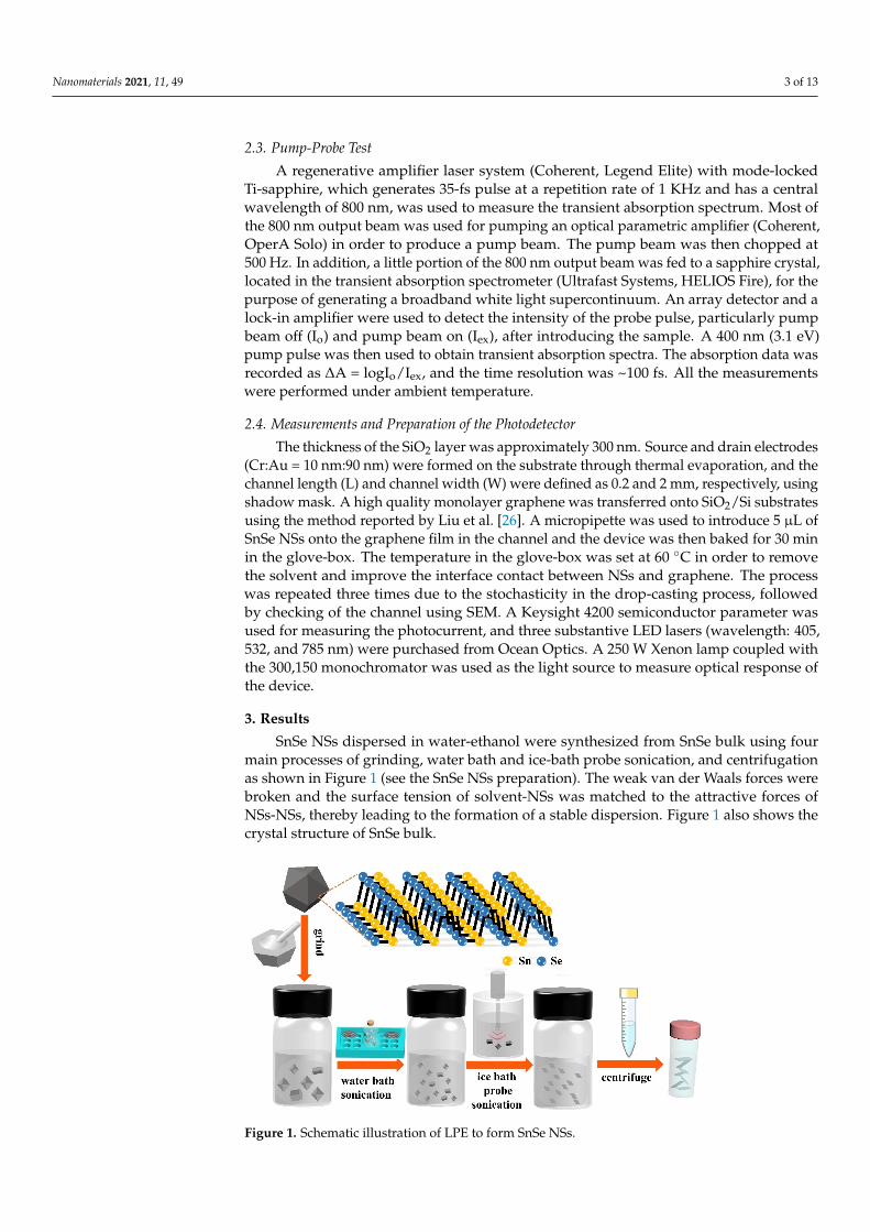
SnSe NSs dispersed in water-ethanol were synthesized from SnSe bulk using fourmain processes of grinding, water bath and ice-bath probe sonication, and centrifugationas shown in Figure 1 (see the SnSe NSs preparation). The weak van der Waals forces werebroken and the surface tension of solvent-NSs was matched to the attractive forces ofNSs-NSs, thereby leading to the formation of a stable dispersion. Figure 1 also shows thecrystal structure of SnSe bulk.
Nanomaterials 2020, 10, x FOR PEER REVIEW 4 of 13
Nanomaterials 2020, 10, x; doi: FOR PEER REVIEW www.mdpi.com/journal/nanomaterials
Figure 1. Schematic illustration of LPE to form SnSe NSs.
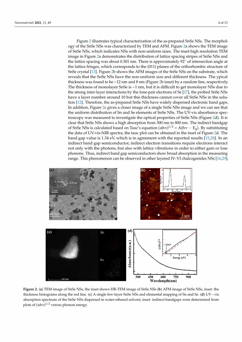
Figure 2 illustrates typical characterization of the as-prepared SnSe NSs. The mor-phology of the SnSe NSs was characterized by TEM and AFM. Figure 2a shows the TEM image of SnSe NSs, which indicates NSs with non-uniform sizes. The inset high resolution TEM image in Figure 2a demonstrates the distribution of lattice spacing stripes of SnSe NSs and the lattice spacing was about 0.301nm. There is approximately 92° of intersection angle at the lattice fringes, which corresponds to the (011) planes of the orthorhombic structure of SnSe crystal [13]. Figure 2b shows the AFM images of the SnSe NSs on the substrate, which reveals that the SnSe NSs have the non-uniform size and different thick-ness. The typical thickness was found to be ~12 nm and 8 nm (Figure 2b inset) by a random line, respectively. The thickness of monolayer SnSe is ~1 nm, but it is difficult to get mon-olayer NSs due to the strong inter-layer interactions by the lone-pair electrons of Se [27], the probed SnSe NSs have a layer number around 10 but this thickness cannot cover all SnSe NSs in the solution [12]. Therefore, the as-prepared SnSe NSs have widely dispersed electronic band gaps. In addition, Figure 2c gives a closer image of a single SnSe NSs im-age and we can see that the uniform distribution of Sn and Se elements of SnSe NSs. The UV-vis absorbance spectroscopy was measured to investigate the optical properties of SnSe NSs (Figure 2d). It is clear that SnSe NSs shows a high absorption from 300 nm to 800 nm. The indirect bandgap of SnSe NSs is calculated based on Tauc’s equation (αhν) / = A(hν − E ). By substituting the data of UV-vis-NIR spectra, the tauc plot can be obtained in the inset of Figure 2d. The band gap value is 1.34 eV, which is in agreement with the reported results [15,28]. In an indirect band gap semiconductor, indirect electron transitions require electrons interact not only with the photons, but also with lattice vibra-tions in order to either gain or lose phonons. Thus, indirect band gap semiconductors show broad absorption in the measuring range. This phenomenon can be observed in other layered IV–VI chalcogenides NSs [16,29].
Figure 1. Schematic illustration of LPE to form SnSe NSs.
Nanomaterials 2021, 11, 49 4 of 13
Figure 2 illustrates typical characterization of the as-prepared SnSe NSs. The morphol-ogy of the SnSe NSs was characterized by TEM and AFM. Figure 2a shows the TEM imageof SnSe NSs, which indicates NSs with non-uniform sizes. The inset high resolution TEMimage in Figure 2a demonstrates the distribution of lattice spacing stripes of SnSe NSs andthe lattice spacing was about 0.301 nm. There is approximately 92◦ of intersection angle atthe lattice fringes, which corresponds to the (011) planes of the orthorhombic structure ofSnSe crystal [13]. Figure 2b shows the AFM images of the SnSe NSs on the substrate, whichreveals that the SnSe NSs have the non-uniform size and different thickness. The ypicalthickness was found to be ~12 nm and 8 nm (Figure 2b inset) by a random line, respectively.The thickness of monolayer SnSe is ~1 nm, but it is difficult to get monolayer NSs due tothe strong inter-layer interactions by the lone-pair electrons of Se [27], the probed SnSe NSshave a layer number around 10 but this thickness cannot cover all SnSe NSs in the solu-tion [12]. Therefore, the as-prepared SnSe NSs have widely dispersed electronic band gaps.In addition, Figure 2c gives a closer image of a single SnSe NSs image and we can see thatthe uniform distribution of Sn and Se elements of SnSe NSs. The UV-vis absorbance spec-troscopy was measured to investigate the optical properties of SnSe NSs (Figure 2d). It isclear that SnSe NSs shows a high absorption from 300 nm to 800 nm. The indirect bandgapof SnSe NSs is calculated based on Tauc’s equation (αhν)1/2 = A(hν − Eg). By substitutingthe data of UV-vis-NIR spectra, the tauc plot can be obtained in the inset of Figure 2d. Theband gap value is 1.34 eV, which is in agreement with the reported results [15,28]. In anindirect band gap semiconductor, indirect electron transitions require electrons interactnot only with the photons, but also with lattice vibrations in order to either gain or losephonons. Thus, indirect band gap semiconductors show broad absorption in the measuringrange. This phenomenon can be observed in other layered IV–VI chalcogenides NSs [16,29].Nanomaterials 2020, 10, x FOR PEER REVIEW 5 of 13
Nanomaterials 2020, 10, x; doi: FOR PEER REVIEW www.mdpi.com/journal/nanomaterials
Figure 2. (a) TEM image of SnSe NSs, the inset shows HR-TEM image of SnSe NSs (b) AFM image of SnSe NSs, inset: the thickness histograms along the red line. (c) A single few-layer SnSe NSs and elemental mapping of Sn and Se. (d) UV−vis absorption spectrum of the SnSe NSs dispersed in water-ethanol solvent, inset: indirect bandgaps were determined from plots of (αhν)1/2 versus pho-non energy.
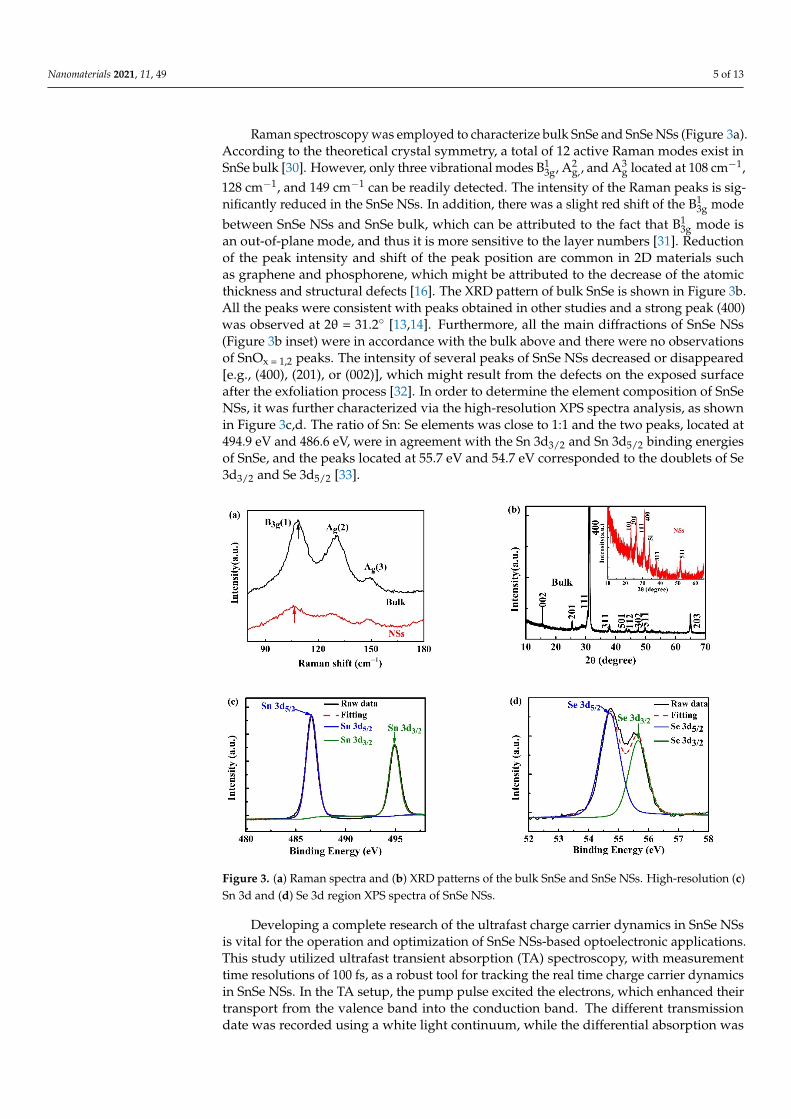
Raman spectroscopy was employed to characterize bulk SnSe and SnSe NSs (Figure 3a). According to the theoretical crystal symmetry, a total of 12 active Raman modes exist in SnSe bulk [30]. However, only three vibrational modes B , A ,, and A located at 108 cm−1, 128 cm−1, and 149 cm−1 can be readily detected. The intensity of the Raman peaks is significantly reduced in the SnSe NSs. In addition, there was a slight red shift of the B mode between SnSe NSs and SnSe bulk, which can be attributed to the fact that B mode is an out-of-plane mode, and thus it is more sensitive to the layer numbers [31]. Reduction of the peak intensity and shift of the peak position are common in 2D materials such as graphene and phosphorene, which might be attributed to the decrease of the atomic thick-ness and structural defects [16]. The XRD pattern of bulk SnSe is shown in Figure 3b. All the peaks were consistent with peaks obtained in other studies and a strong peak (400) was observed at 2θ = 31.2° [13,14]. Furthermore, all the main diffractions of SnSe NSs (Fig-ure 3b inset) were in accordance with the bulk above and there were no observations of SnOx = 1,2 peaks. The intensity of several peaks of SnSe NSs decreased or disappeared [e.g., (400), (201), or (002)], which might result from the defects on the exposed surface after the exfoliation process [32]. In order to determine the element composition of SnSe NSs, it was further characterized via the high-resolution XPS spectra analysis, as shown in Figure 3c and 3d. The ratio of Sn: Se elements was close to 1:1 and the two peaks, located at 494.9 eV and 486.6 eV, were in agreement with the Sn 3d3/2 and Sn 3d5/2 binding energies of SnSe, and the peaks located at 55.7 eV and 54.7 eV corresponded to the doublets of Se 3d3/2 and Se 3d5/2 [33].
Figure 2. (a) TEM image of SnSe NSs, the inset shows HR-TEM image of SnSe NSs (b) AFM image of SnSe NSs, inset: thethickness histograms along the red line. (c) A single few-layer SnSe NSs and elemental mapping of Sn and Se. (d) UV−visabsorption spectrum of the SnSe NSs dispersed in water-ethanol solvent, inset: indirect bandgaps were determined fromplots of (αhν)1/2 versus phonon energy.
Nanomaterials 2021, 11, 49 5 of 13
Raman spectroscopy was employed to characterize bulk SnSe and SnSe NSs (Figure 3a).According to the theoretical crystal symmetry, a total of 12 active Raman modes exist inSnSe bulk [30]. However, only three vibrational modes B1
3g, A2g,, and A3
g located at 108 cm−1,128 cm−1, and 149 cm−1 can be readily detected. The intensity of the Raman peaks is sig-nificantly reduced in the SnSe NSs. In addition, there was a slight red shift of the B1
3g modebetween SnSe NSs and SnSe bulk, which can be attributed to the fact that B1
3g mode isan out-of-plane mode, and thus it is more sensitive to the layer numbers [31]. Reductionof the peak intensity and shift of the peak position are common in 2D materials suchas graphene and phosphorene, which might be attributed to the decrease of the atomicthickness and structural defects [16]. The XRD pattern of bulk SnSe is shown in Figure 3b.All the peaks were consistent with peaks obtained in other studies and a strong peak (400)was observed at 2θ = 31.2◦ [13,14]. Furthermore, all the main diffractions of SnSe NSs(Figure 3b inset) were in accordance with the bulk above and there were no observationsof SnOx = 1,2 peaks. The intensity of several peaks of SnSe NSs decreased or disappeared[e.g., (400), (201), or (002)], which might result from the defects on the exposed surfaceafter the exfoliation process [32]. In order to determine the element composition of SnSeNSs, it was further characterized via the high-resolution XPS spectra analysis, as shownin Figure 3c,d. The ratio of Sn: Se elements was close to 1:1 and the two peaks, located at494.9 eV and 486.6 eV, were in agreement with the Sn 3d3/2 and Sn 3d5/2 binding energiesof SnSe, and the peaks located at 55.7 eV and 54.7 eV corresponded to the doublets of Se3d3/2 and Se 3d5/2 [33].Nanomaterials 2020, 10, x FOR PEER REVIEW 6 of 13
Nanomaterials 2020, 10, x; doi: FOR PEER REVIEW www.mdpi.com/journal/nanomaterials
Figure 3. (a) Raman spectra and (b) XRD patterns of the bulk SnSe and SnSe NSs. High-resolution (c) Sn 3d and (d) Se 3d region XPS spectra of SnSe NSs.
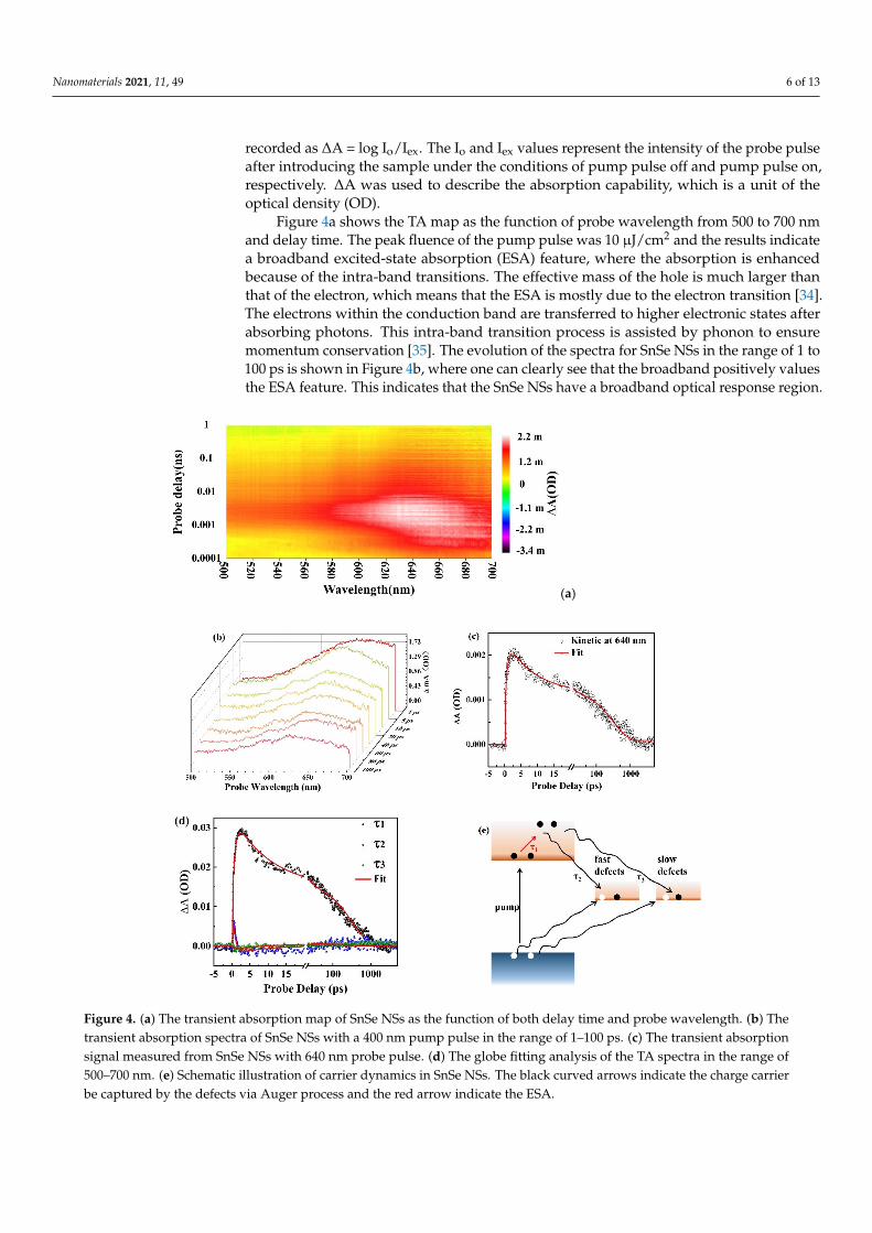
Developing a complete research of the ultrafast charge carrier dynamics in SnSe NSs is vital for the operation and optimization of SnSe NSs-based optoelectronic applications. This study utilized ultrafast transient absorption (TA) spectroscopy, with measurement time resolutions of 100 fs, as a robust tool for tracking the real time charge carrier dynam-ics in SnSe NSs. In the TA setup, the pump pulse excited the electrons, which enhanced their transport from the valence band into the conduction band. The different transmis-sion date was recorded using a white light continuum, while the differential absorption was recorded as ∆A = log I /I . The I and I values represent the intensity of the probe pulse after introducing the sample under the conditions of pump pulse off and pump pulse on, respectively. ∆A was used to describe the absorption capability, which is a unit of the optical density (OD).
Figure 4a shows the TA map as the function of probe wavelength from 500 to 700nm and delay time. The peak fluence of the pump pulse was 10 µJ/cm2 and the results indicate a broadband excited-state absorption (ESA) feature, where the absorption is enhanced be-cause of the intra-band transitions. The effective mass of the hole is much larger than that of the electron, which means that the ESA is mostly due to the electron transition [34]. The electrons within the conduction band are transferred to higher electronic states after ab-sorbing photons. This intra-band transition process is assisted by phonon to ensure mo-mentum conservation [35]. The evolution of the spectra for SnSe NSs in the range of 1 to 100 ps is shown in Figure 4b, where one can clearly see that the broadband positively values the ESA feature. This indicates that the SnSe NSs have a broadband optical re-sponse region.
The ESA reflects the evolution of energized electrons. The TA signal at positive max-ima around 640 nm (Figure 4c) was well fitted using tri-exponential model. It is a signal-wavelength kinetic analysis, and we obtain three time-constants: τ1 (0.759 ps), τ2 (8.01 ps), and τ3 (329 ps). In addition, the recovery time was very fast, which exactly demonstrates that SnSe NSs have a great potential for application in high-speed photodetectors. Globe fitting is an effective analytical method for complex spectra. We perform the globe fitting analysis of the TA spectra in the range of 500–700 nm. The kinetic curves of three principal components are shown in Figure 4d and we get three time-constants, τ1′ (0.77 ps), τ2′ (8.3 ps), and τ3′ (316.5 ps), which coincide with the fitting results of Figure 4c. The time constant
Figure 3. (a) Raman spectra and (b) XRD patterns of the bulk SnSe and SnSe NSs. High-resolution (c)Sn 3d and (d) Se 3d region XPS spectra of SnSe NSs.
Developing a complete research of the ultrafast charge carrier dynamics in SnSe NSsis vital for the operation and optimization of SnSe NSs-based optoelectronic applications.This study utilized ultrafast transient absorption (TA) spectroscopy, with measurementtime resolutions of 100 fs, as a robust tool for tracking the real time charge carrier dynamicsin SnSe NSs. In the TA setup, the pump pulse excited the electrons, which enhanced theirtransport from the valence band into the conduction band. The different transmissiondate was recorded using a white light continuum, while the differential absorption was
Nanomaterials 2021, 11, 49 6 of 13
recorded as ∆A = log Io/Iex. The Io and Iex values represent the intensity of the probe pulseafter introducing the sample under the conditions of pump pulse off and pump pulse on,respectively. ∆A was used to describe the absorption capability, which is a unit of theoptical density (OD).
Figure 4a shows the TA map as the function of probe wavelength from 500 to 700 nmand delay time. The peak fluence of the pump pulse was 10 µJ/cm2 and the results indicatea broadband excited-state absorption (ESA) feature, where the absorption is enhancedbecause of the intra-band transitions. The effective mass of the hole is much larger thanthat of the electron, which means that the ESA is mostly due to the electron transition [34].The electrons within the conduction band are transferred to higher electronic states afterabsorbing photons. This intra-band transition process is assisted by phonon to ensuremomentum conservation [35]. The evolution of the spectra for SnSe NSs in the range of 1 to100 ps is shown in Figure 4b, where one can clearly see that the broadband positively valuesthe ESA feature. This indicates that the SnSe NSs have a broadband optical response region.
Nanomaterials 2020, 10, x FOR PEER REVIEW 7 of 13
Nanomaterials 2020, 10, x; doi: FOR PEER REVIEW www.mdpi.com/journal/nanomaterials
τ1 (0.77 ps) can be attributed to the process of ESA, where the electrons were transferred to higher electronic states after absorbing photons. A strong quantum confinement effect and a reduced dielectric screening effect can result in strong Coulomb interactions be-tween the electrons and holes, which induce the Auger processes effective for carrier cap-ture by defects. The carrier capture processes via Auger recombination can realize even at relatively low carrier densities. There are different types of defect states in the SnSe NSs and defect states have different capturing rates for charge carriers. The other two time-constants τ2 (8.3 ps) and τ3 (316.5 ps) correspond to the two decay lifetimes of the carriers captured by the two different deep mid-gap defects states in SnSe NSs. One of the pro-cesses is fast, and the other process is slow. The defects are named as the fast defects and the slow defects [36–38]. In these processes, the excess energy of the electrons and holes is released by exciting other electrons or holes, thereby helping them attain higher energy states [39]. However, there is a different mode where the long recovery time results from the bonding excitons in the defect states, which block the fast recombination [16,40]. Fur-ther studies on the detailed recovery mechanism should be conducted.
(a)
Figure 4. (a) The transient absorption map of SnSe NSs as the function of both delay time and probe wavelength. (b) The transient absorption spectra of SnSe NSs with a 400 nm pump pulse in the range of 1–100 ps. (c) The transient absorption signal measured from SnSe NSs with 640 nm probe pulse. (d) The globe fitting analysis of the TA spectra in the range of 500–700 nm. (e) Sche-matic illustration of carrier dynamics in SnSe NSs. The black curved arrows indicate the charge carrier be captured by the defects via Auger process and the red arrow indicate the ESA.
Figure 4. (a) The transient absorption map of SnSe NSs as the function of both delay time and probe wavelength. (b) Thetransient absorption spectra of SnSe NSs with a 400 nm pump pulse in the range of 1–100 ps. (c) The transient absorptionsignal measured from SnSe NSs with 640 nm probe pulse. (d) The globe fitting analysis of the TA spectra in the range of500–700 nm. (e) Schematic illustration of carrier dynamics in SnSe NSs. The black curved arrows indicate the charge carrierbe captured by the defects via Auger process and the red arrow indicate the ESA.
Nanomaterials 2021, 11, 49 7 of 13
The ESA reflects the evolution of energized electrons. The TA signal at positive max-ima around 640 nm (Figure 4c) was well fitted using tri-exponential model. It is a signal-wavelength kinetic analysis, and we obtain three time-constants: τ1 (0.759 ps), τ2 (8.01 ps),and τ3 (329 ps). In addition, the recovery time was very fast, which exactly demonstratesthat SnSe NSs have a great potential for application in high-speed photodetectors. Globefitting is an effective analytical method for complex spectra. We perform the globe fittinganalysis of the TA spectra in the range of 500–700 nm. The kinetic curves of three prin-cipal components are shown in Figure 4d and we get three time-constants, τ1′ (0.77 ps),τ2′ (8.3 ps), and τ3′ (316.5 ps), which coincide with the fitting results of Figure 4c. The timeconstant τ1 (0.77 ps) can be attributed to the process of ESA, where the electrons were trans-ferred to higher electronic states after absorbing photons. A strong quantum confinementeffect and a reduced dielectric screening effect can result in strong Coulomb interactionsbetween the electrons and holes, which induce the Auger processes effective for carriercapture by defects. The carrier capture processes via Auger recombination can realize evenat relatively low carrier densities. There are different types of defect states in the SnSeNSs and defect states have different capturing rates for charge carriers. The other twotime-constants τ2 (8.3 ps) and τ3 (316.5 ps) correspond to the two decay lifetimes of thecarriers captured by the two different deep mid-gap defects states in SnSe NSs. One of theprocesses is fast, and the other process is slow. The defects are named as the fast defectsand the slow defects [36–38]. In these processes, the excess energy of the electrons andholes is released by exciting other electrons or holes, thereby helping them attain higherenergy states [39]. However, there is a different mode where the long recovery time resultsfrom the bonding excitons in the defect states, which block the fast recombination [16,40].Further studies on the detailed recovery mechanism should be conducted.
We proposed the ultrafast dynamic processes of charge carriers in SnSe NSs basedon recent reports [36] and results obtained in this study (Figure 4e). The electrons arefirst transported from the valence band into the conduction band under pump excitation.Afterwards, they are transported to the higher states after absorbing photons, and theelectrons are assisted by phonon to satisfy the momentum conservation. Subsequently,the fast defects states will capture a part of the electrons and holes, within a few ps, throughthe Auger process. After occupation of the fast defect states, the remaining charge carrierswill be captured by slow defects, thereby resulting in the slow recombination process.
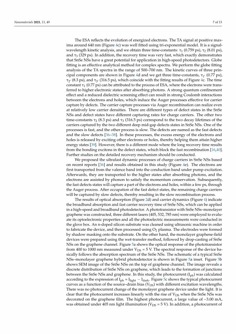
The results of optical absorption (Figure 2d) and carrier dynamics (Figure 4) indicatethe broadband absorption and fast carrier recovery time of SnSe NSs, which can be appliedin a high-speed and broadband photodetector. A phototransistor with SnSe NSs–monolayergraphene was constructed, three different lasers (405, 532, 785 nm) were employed to evalu-ate its optoelectronic properties and all the photoelectric measurements were conducted inthe glove box. An n-doped silicon substrate was cleaned using ultrasonic machine in orderto fabricate the device, and then processed using O2 plasma. The electrodes were formedby shadow masking onto the substrate. On the other hand, the monolayer graphene-fielddevices were prepared using the wet-transfer method, followed by drop-casting of SnSeNSs on the graphene channel. Figure 5a shows the optical response of the phototransistorfrom 400 to 1000 nm measured under VDS = 5 V. The spectral response of the device ba-sically follows the absorption spectrum of the SnSe NSs. The schematic of a typical SnSeNSs–monolayer graphene hybrid photodetector is shown in Figure 5a inset. Figure 5bshows SEM image of the SnSe NSs on the top of graphene channel. The image reveals adiscrete distribution of SnSe NSs on graphene, which leads to the formation of junctionsbetween the SnSe NSs and graphene. In this study, the photocurrent (Iph) was calculatedaccording to the expression of Iph = Ilight − Idark. Figure 5c shows the typical photocurrentcurves as a function of the source–drain bias (VDS) with different excitation wavelengths.There was no photocurrent change of the monolayer graphene device under the light. It isclear that the photocurrent increases linearly with the rise of VDS when the SnSe NSs wasdecorated on the graphene film. The highest photocurrent, a large value of ~3.00 mA,was obtained under 405 nm light illumination (VDS = 5 V). In addition, a photocurrent of
Nanomaterials 2021, 11, 49 8 of 13
~2.04 mA was observed under light illumination of 532 nm. Increasing the wavelength ledsto the hybrid device displaying a photocurrent of ~0.95 mA under 785 nm illumination. Thecurrent change of photodetector can be attributed to the carrier accumulation in graphene,which are formed from charge transfer after optical excitation. The photoresponsivity (Rph)is calculated as Rph = Iph/P, where P is defined as incident optical power. Indeed, it isfound that the maximum responsivity is about 1.75× 10⁴ A/W while illuminated at 405 nmwith a radiation density of 23.6 µW/cm2, as shown in Figure 5d. It is worth noting thatthe channel length (200 µM) was larger than the length reported in previous SnSe-basedphotodetector studies [12,13,19,40]. Figure 5d also demonstrates that the responsivitydecreases with the increase of light wavelength. The maximum responsivity under the785 nm is found to be 1.52 × 10³ A/W at the power density of 155.2 µW/cm2.Nanomaterials 2020, 10, x FOR PEER REVIEW 9 of 13
Nanomaterials 2020, 10, x; doi: FOR PEER REVIEW www.mdpi.com/journal/nanomaterials
Figure 5. (a) Spectral response of the graphene–SnSe NSs photodetector. Inset: schematic diagram of the graphene–SnSe NSs photodetector. (b) SEM image of the SnSe NSs on the graphene film. (c) Photocurrent of the hybrid device under different light wavelength as a function of VDS (Light power density of 155.2 μW/cm2, VG = 0 V). The photocurrent for the only graphene device shows a negligible effect. (d) Responsivities as a function of VDS (VG = 0 V) under different light wave-length, each with the lowest power intensity.
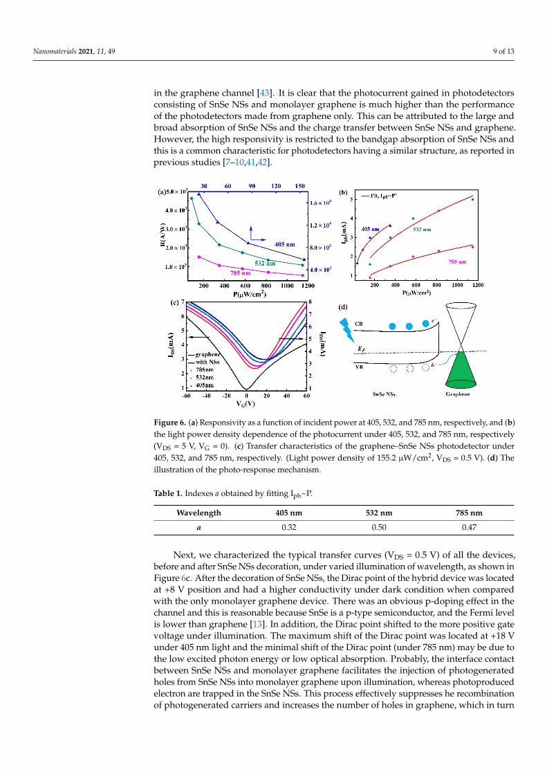
The responsivity as a function of radiation density for different wavelength is sum-marized in Figure 6a. It can be seen that the corresponding responsivity decreased non-linearly when the incident power was turned up. This may be due to the increase of the concentration of photoexcited carriers under higher incident power, which results in the carriers forming an electrical field and the formed electrical field is in reverse to the built-in field, thereby hindering the transport of photogenerated electron-hole pairs. The same change was reported in previous studies which constructed monolayer graphene photo-detectors with a similar structure [5–10,41,42]. Furthermore, the responsivity reduced as the wavelength of light increases, which basically follows the absorption spectrum of the SnSe NSs (Figure 2d). The dependence between the incident light power density and the photocurrent can be determined using the following law: I = CP , where C represents the proportional constant and the index, and a denotes the ideal factor of photocurrent to light power density. For the ideal photodetector, the a = 1.0. The a value can be determined by fitting the curves as shown in Figure 6b and the ideal factor a are displayed in Table 1. The values of a are vary from 0.32 to 0.50. which demonstrate that the carrier generations exist in the graphene channel [43]. It is clear that the photocurrent gained in photodetec-tors consisting of SnSe NSs and monolayer graphene is much higher than the performance of the photodetectors made from graphene only. This can be attributed to the large and broad absorption of SnSe NSs and the charge transfer between SnSe NSs and graphene. However, the high responsivity is restricted to the bandgap absorption of SnSe NSs and this is a common characteristic for photodetectors having a similar structure, as reported in previous studies [7–10,41,42].
Figure 5. (a) Spectral response of the graphene–SnSe NSs photodetector. Inset: schematic diagramof the graphene–SnSe NSs photodetector. (b) SEM image of the SnSe NSs on the graphene film.(c) Photocurrent of the hybrid device under different light wavelength as a function of VDS (Lightpower density of 155.2 µW/cm2, VG = 0 V). The photocurrent for the only graphene device shows anegligible effect. (d) Responsivities as a function of VDS (VG = 0 V) under different light wavelength,each with the lowest power intensity.
The responsivity as a function of radiation density for different wavelength is summa-rized in Figure 6a. It can be seen that the corresponding responsivity decreased nonlinearlywhen the incident power was turned up. This may be due to the increase of the concen-tration of photoexcited carriers under higher incident power, which results in the carriersforming an electrical field and the formed electrical field is in reverse to the built-in field,thereby hindering the transport of photogenerated electron-hole pairs. The same changewas reported in previous studies which constructed monolayer graphene photodetectorswith a similar structure [5–10,41,42]. Furthermore, the responsivity reduced as the wave-length of light increases, which basically follows the absorption spectrum of the SnSeNSs (Figure 2d). The dependence between the incident light power density and the pho-tocurrent can be determined using the following law: Iph = CPa, where C represents theproportional constant and the index, and a denotes the ideal factor of photocurrent to lightpower density. For the ideal photodetector, the a = 1.0. The a value can be determined byfitting the curves as shown in Figure 6b and the ideal factor a are displayed in Table 1. Thevalues of a are vary from 0.32 to 0.50. which demonstrate that the carrier generations exist
Nanomaterials 2021, 11, 49 9 of 13
in the graphene channel [43]. It is clear that the photocurrent gained in photodetectorsconsisting of SnSe NSs and monolayer graphene is much higher than the performanceof the photodetectors made from graphene only. This can be attributed to the large andbroad absorption of SnSe NSs and the charge transfer between SnSe NSs and graphene.However, the high responsivity is restricted to the bandgap absorption of SnSe NSs andthis is a common characteristic for photodetectors having a similar structure, as reported inprevious studies [7–10,41,42].Nanomaterials 2020, 10, x FOR PEER REVIEW 10 of 13
Nanomaterials 2020, 10, x; doi: FOR PEER REVIEW www.mdpi.com/journal/nanomaterials
Figure 6. (a) Responsivity as a function of incident power at 405, 532, and 785 nm, respectively, and (b) the light power density dependence of the photocurrent under 405, 532, and 785 nm, re-spectively (VDS = 5 V, VG = 0). (c) Transfer characteristics of the graphene–SnSe NSs photodetector under 405, 532, and 785 nm, respectively. (Light power density of 155.2 μW/cm2, VDS = 0.5 V). (d) The illustration of the photo-response mechanism.
Table 1. Indexes a obtained by fitting I ~P.
Wavelength 405 nm 532 nm 785 nm a 0.32 0.50 0.47
Next, we characterized the typical transfer curves (V = 0.5 V) of all the devices, before and after SnSe NSs decoration, under varied illumination of wavelength, as shown in Figure 6c. After the decoration of SnSe NSs, the Dirac point of the hybrid device was located at +8 V position and had a higher conductivity under dark condition when com-pared with the only monolayer graphene device. There was an obvious p-doping effect in the channel and this is reasonable because SnSe is a p-type semiconductor, and the Fermi level is lower than graphene [13]. In addition, the Dirac point shifted to the more positive gate voltage under illumination. The maximum shift of the Dirac point was located at +18 V under 405 nm light and the minimal shift of the Dirac point (under 785 nm) may be due to the low excited photon energy or low optical absorption. Probably, the interface contact between SnSe NSs and monolayer graphene facilitates the injection of photogenerated holes from SnSe NSs into monolayer graphene upon illumination, whereas photopro-duced electron are trapped in the SnSe NSs. This process effectively suppresses he recom-bination of photogenerated carriers and increases the number of holes in graphene, which in turn gives a clear photocurrent [7,43–45]. Figure 6d displays the schematic of photo-response scenario, which can further explain this phenomenon.
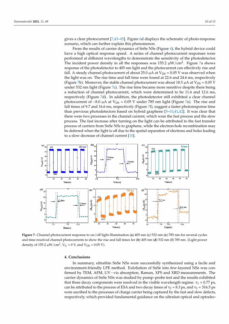
From the results of carrier dynamics of SnSe NSs (Figure 4), the hybrid device could have a high optical response speed. A series of channel photocurrent responses were per-formed at different wavelengths to demonstrate the sensitivity of the photodetector. The incident power density in all the responses was 155.2 µW/cm2. Figure 7a shows response of the photodetector to 405nm light and the photocurrent can effectively rise and fall. A steady channel photocurrent of about 25.0 µA at V = 0.05 V was observed when the light was on. The rise time and fall time were found at 22.6 and 24.6 ms, respectively (Fig-ure 7b). Moreover, the stable channel photocurrent was about 18.5 µA at V = 0.05 V under 532 nm light (Figure 7c). The rise time became more sensitive despite there being a
Figure 6. (a) Responsivity as a function of incident power at 405, 532, and 785 nm, respectively, and (b)the light power density dependence of the photocurrent under 405, 532, and 785 nm, respectively(VDS = 5 V, VG = 0). (c) Transfer characteristics of the graphene–SnSe NSs photodetector under405, 532, and 785 nm, respectively. (Light power density of 155.2 µW/cm2, VDS = 0.5 V). (d) Theillustration of the photo-response mechanism.
Table 1. Indexes a obtained by fitting Iph~P.
Wavelength 405 nm 532 nm 785 nm
a 0.32 0.50 0.47
Next, we characterized the typical transfer curves (VDS = 0.5 V) of all the devices,before and after SnSe NSs decoration, under varied illumination of wavelength, as shown inFigure 6c. After the decoration of SnSe NSs, the Dirac point of the hybrid device was locatedat +8 V position and had a higher conductivity under dark condition when comparedwith the only monolayer graphene device. There was an obvious p-doping effect in thechannel and this is reasonable because SnSe is a p-type semiconductor, and the Fermi levelis lower than graphene [13]. In addition, the Dirac point shifted to the more positive gatevoltage under illumination. The maximum shift of the Dirac point was located at +18 Vunder 405 nm light and the minimal shift of the Dirac point (under 785 nm) may be due tothe low excited photon energy or low optical absorption. Probably, the interface contactbetween SnSe NSs and monolayer graphene facilitates the injection of photogeneratedholes from SnSe NSs into monolayer graphene upon illumination, whereas photoproducedelectron are trapped in the SnSe NSs. This process effectively suppresses he recombinationof photogenerated carriers and increases the number of holes in graphene, which in turn
Nanomaterials 2021, 11, 49 10 of 13
gives a clear photocurrent [7,43–45]. Figure 6d displays the schematic of photo-responsescenario, which can further explain this phenomenon.
From the results of carrier dynamics of SnSe NSs (Figure 4), the hybrid device couldhave a high optical response speed. A series of channel photocurrent responses wereperformed at different wavelengths to demonstrate the sensitivity of the photodetector.The incident power density in all the responses was 155.2 µW/cm2. Figure 7a showsresponse of the photodetector to 405 nm light and the photocurrent can effectively rise andfall. A steady channel photocurrent of about 25.0 µA at VDS = 0.05 V was observed whenthe light was on. The rise time and fall time were found at 22.6 and 24.6 ms, respectively(Figure 7b). Moreover, the stable channel photocurrent was about 18.5 µA at VDS = 0.05 Vunder 532 nm light (Figure 7c). The rise time became more sensitive despite there beinga reduction of channel photocurrent, which were determined to be 11.6 and 12.6 ms,respectively (Figure 7d). In addition, the photodetector still exhibited a clear channelphotocurrent of ~8.0 µA at VDS = 0.05 V under 785 nm light (Figure 7e). The rise andfall times of 9.7 and 16.6 ms, respectively (Figure 7f), suggest a faster photoresponse timethan previous photodetectors based on hybrid graphene [5–10,41,42]. It was clear thatthere were two processes in the channel current, which were the fast process and the slowprocess. The fast increase after turning on the light can be attributed to the fast transferprocess of carriers from SnSe NSs to graphene, while the electron-hole recombination maybe deferred when the light is off due to the spatial separation of electrons and holes leadingto a slow decrease of channel current [10].
Nanomaterials 2020, 10, x FOR PEER REVIEW 11 of 13
Nanomaterials 2020, 10, x; doi: FOR PEER REVIEW www.mdpi.com/journal/nanomaterials
reduction of channel photocurrent, which were determined to be 11.6 and 12.6 ms, respec-tively (Figure 7d). In addition, the photodetector still exhibited a clear channel photocur-rent of ~8.0 µA at V = 0.05 V under 785 nm light (Figure 7e). The rise and fall times of 9.7 and 16.6 ms, respectively (Figure 7f), suggest a faster photoresponse time than previ-ous photodetectors based on hybrid graphene [5–10,41,42]. It was clear that there were two processes in the channel current, which were the fast process and the slow process. The fast increase after turning on the light can be attributed to the fast transfer process of carriers from SnSe NSs to graphene, while the electron-hole recombination may be de-ferred when the light is off due to the spatial separation of electrons and holes leading to a slow decrease of channel current [10].
Figure 7. Channel photocurrent response to on/off light illumination (a) 405 nm (c) 532nm (e) 785 nm for several cycles and time-resolved channel photocurrents to show the rise and fall times for (b) 405 nm (d) 532nm (f) 785 nm. (Light power density of 155.2 μW/cm2, VG = 0 V, and VDS = 0.05 V).
4. Conclusions In summary, ultrathin SnSe NSs were successfully synthesized using a facile and en-
vironment-friendly LPE method. Exfoliation of SnSe into few-layered NSs was confirmed by TEM, AFM, UV−vis absorption, Raman, XPS and XRD measurements. The carrier dy-namics of SnSe NSs was studied by pump–probe test and the results exhibited that three decay components were resolved in the visible wavelength regime: τ = 0.77 ps, can be attributed to the process of ESA and two decay times of τ = 8.3 ps, and τ = 316.5 ps were ascribed to the processes of charge carrier being captured by the fast and slow de-fects, respectively, which provided fundamental guidance on the ultrafast optical and op-toelectronic properties of this novel material. Application of the SnSe NSs for an absorp-tion medium on the monolayer graphene resulted in the photodetector exhibiting high responsivity and a fast response speed from the 405 nm to 785 nm. The obtained results indicated that the responsivity was up to 1.75 × 10⁴ A/W, 4.63 × 10³ A/W, and 1.52 × 10³ A/W under 405, 532, and 785 nm light, respectively, and the photoresponse time was ~22.6, 11.6, and 9.7 ms. The photosensing mechanisms arise from several important factors, such as the high and broad absorptivity of SnSe NSs, high conductivity of monolayer graphene, the charge transfer between SnSe NSs and graphene and the fast carrier recovery time in the SnSe NSs. In addition, this study has also systematically revealed the effects of light wave-length and light power density on the behavior of photoresponse. The advantages of en-vironment-friendliness and a facile fabrication process in this study indicate that the SnSe NSs could be used as a new 2D semiconductor nanomaterial. The broad photodetection
Figure 7. Channel photocurrent response to on/off light illumination (a) 405 nm (c) 532 nm (e) 785 nm for several cyclesand time-resolved channel photocurrents to show the rise and fall times for (b) 405 nm (d) 532 nm (f) 785 nm. (Light powerdensity of 155.2 µW/cm2, VG = 0 V, and VDS = 0.05 V).
4. Conclusions
In summary, ultrathin SnSe NSs were successfully synthesized using a facile andenvironment-friendly LPE method. Exfoliation of SnSe into few-layered NSs was con-firmed by TEM, AFM, UV−vis absorption, Raman, XPS and XRD measurements. Thecarrier dynamics of SnSe NSs was studied by pump–probe test and the results exhibitedthat three decay components were resolved in the visible wavelength regime: τ1 = 0.77 ps,can be attributed to the process of ESA and two decay times of τ2 = 8.3 ps, and τ3 = 316.5 pswere ascribed to the processes of charge carrier being captured by the fast and slow defects,respectively, which provided fundamental guidance on the ultrafast optical and optoelec-
Nanomaterials 2021, 11, 49 11 of 13
tronic properties of this novel material. Application of the SnSe NSs for an absorptionmedium on the monolayer graphene resulted in the photodetector exhibiting high respon-sivity and a fast response speed from the 405 nm to 785 nm. The obtained results indicatedthat the responsivity was up to 1.75 × 10⁴ A/W, 4.63 × 10³ A/W, and 1.52 × 10³ A/Wunder 405, 532, and 785 nm light, respectively, and the photoresponse time was ~22.6, 11.6,and 9.7 ms. The photosensing mechanisms arise from several important factors, such asthe high and broad absorptivity of SnSe NSs, high conductivity of monolayer graphene,the charge transfer between SnSe NSs and graphene and the fast carrier recovery time inthe SnSe NSs. In addition, this study has also systematically revealed the effects of lightwavelength and light power density on the behavior of photoresponse. The advantagesof environment-friendliness and a facile fabrication process in this study indicate thatthe SnSe NSs could be used as a new 2D semiconductor nanomaterial. The broad pho-todetection performance demonstrates the obtained SnSe NSs-based monolayer graphenephotodetector can be an excellent candidate for photonics device.
Author Contributions: Data curation, X.L., Z.S. (Zongpeng Song), and H.Z. (Huancheng Zhao);formal analysis, L.L., H.L., and J.P.; resources, S.R., W.Z., H.Z. (Haiou Zhu), and Z.S. (Zhenhua Sun);writing—review and editing, L.L. All authors have read and agreed to the published version of themanuscript.
Funding: This work was supported by Science and Technology Projects of Shenzhen(JCYJ20180305125000525) and (JCYJ20170817095017389).
Data Availability Statement: The data are not publicly available due to privacy.
Conflicts of Interest: The authors declare no conflict of interest.
References1. Bonaccorso, F.; Sun, Z.; Hasan, T.; Ferrari, A.C. Graphene photonics and optoelectronics. Nat. Photon. 2010, 4, 611–622. [CrossRef]2. Xia, F.; Thomas, M.; Lin, Y.; Valdes, Y.; Phaedon, A. Ultrafast Graphene Phototransistor. Nat. Nanotechnol. 2009, 4, 839–843.
[CrossRef] [PubMed]3. Li, X.; Li, T.; Chen, Z.; Fang, H.; Li, X.; Wang, X.; Xu, J.; Zhu, H. Graphene and Related Two-Dimensional Materials: Struc-ture-
property Relationships for Electronics and Optoelectronics. Appl. Phys. Rev. 2017, 4, 021306. [CrossRef]4. Mueller, T.; Xia, F.; Phaedon, A. Graphene Phototransistors for High-Speed Optical Communications. Nat. Photonics
2010, 4, 297–301. [CrossRef]5. Konstantatos, G.; Badioli, M.; Gaudreau, L.; Osmond, J.; Bernechea, M.; De Arquer, F.P.G.; Gatti, F.; Koppens, F.H.L. Hybrid
graphene–quantum dot phototransistors with ultrahigh gain. Nat. Nanotechnol. 2012, 7, 363–368. [CrossRef] [PubMed]6. Nguyen, K.T.; Li, D.; Borah, P.; Ma, X.; Liu, Z.; Zhu, L.; Gruner, G.; Xiong, Q.; Zhao, Y. Photoinduced Charge Transfer within
Polyaniline-Encapsulated Quantum Dots Decorated on Graphene. ACS Appl. Mater. Interfaces 2013, 5, 8105–8110. [CrossRef][PubMed]
7. Sun, Z.; Liu, Z.; Li, J.; Tai, G.A.; Lau, S.P.; Yan, F. Infrared Phototransistors Based on CVD-grown Graphene and PbS Quan-tumDots with Ultrahigh Responsivity. Adv. Mater. 2012, 24, 5878–5883. [CrossRef]
8. Sun, Y.-L.; Xie, D.; Sun, M.-X.; Teng, C.-J.; Qian, L.; Chen, R.-S.; Xiang, L.; Ren, T.-L. Hybrid graphene/cadmium-free ZnSe/ZnSquantum dots phototransistors for UV detection. Sci. Rep. 2018, 8, 5107. [CrossRef]
9. Lai, S.K.; Xie, C.; Teng, K.S.; Li, Y.; Tan, F.; Yan, F.; Lau, S.P. Polymeric Carbon Nitride Nanosheets/Graphene Hybrid Phototransis-tors with High Responsivity. Adv. Opt. Mater. 2016, 4, 555–561. [CrossRef]
10. Cheng, S.-H.; Weng, T.-M.; Lu, M.-L.; Tan, W.-C.; Chen, J.-Y.; Chen, Y.-F. All Carbon-Based Photodetectors: An eminent integrationof graphite quantum dots and two dimensional graphene. Sci. Rep. 2013, 3, 2694. [CrossRef]
11. Bayat, A.; Saievar-Iranizad, E. Synthesis of blue photoluminescent WS 2 quantum dots via ultrasonic cavitation. J. Lumin.2017, 185, 236–240. [CrossRef]
12. Li, L.; Chen, Z.; Hu, Y.; Wang, X.; Zhang, T.; Chen, W.; Wang, Q. Single-layer Single-crystalline SnSe Nanosheets. J. Am. Chem. Soc.2013, 135, 1213–1216. [CrossRef] [PubMed]
13. Jia, Z.; Xiang, J.; Wen, F.; Yang, R.; Hao, C.; Liu, Z. Enhanced Photoresponse of SnSe-nanocrystals-decorated WS2 MonolayerPhototransistor. ACS App Mater. Inter. 2016, 8, 4781–4788. [CrossRef]
14. Ren, X.; Qi, X.; Shen, Y.; Xu, G.; Li, J.; Li, Z.; Zhong, J. Synthesis of SnSe Nanosheets by Hydrothermal Intercalation and ExfoliationRoute and Their Pho-toresponse Properties. Mater. Sci. Eng. B 2016, 214, 46–50. [CrossRef]
15. Huang, Y.; Li, L.; Lin, Y.-H.; Nan, C.-W. Liquid Exfoliation Few-Layer SnSe Nanosheets with Tunable Band Gap. J. Phys. Chem. C2017, 121, 17530–17537. [CrossRef]

Nanomaterials 2021, 11, 49 12 of 13
16. Ye, Y.; Xian, Y.; Cai, J.; Lu, K.; Liu, Z.; Shi, T.; Du, J.; Leng, Y.; Wei, R.; Wang, W.; et al. Linear and Nonlinear Optical Properties ofFew-Layer Exfoliated SnSe Nanosheets. Adv. Opt. Mater. 2019, 7, 1800579. [CrossRef]
17. Khan, H.; Mahmood, N.; Zavabeti, A.; Elbourne, A.; Rahman, A.; Zhang, B.Y.; Krishnamurthi, V.; Atkin, P.; Wang, D.; Yang, J.;et al. Liquid metal-based synthesis of high performance monolayer SnS piezoelectric nanogenerators. Nat. Commun. 2020, 11, 1–8.[CrossRef]
18. Krishnamurthi, V.; Khan, H.; Ahmed, T.; Zavabeti, A.; Tawfik, S.A.; Jain, S.K.; Fu, L. Liquid-Metal Synthesized Ultrathin SnSLayers for High-Performance Broadband Photodetectors. Adv. Mater. 2020, 32, 4247. [CrossRef]
19. Zhao, S.; Wang, H.; Zhou, Y.; Liao, L.; Jiang, Y.; Yang, X.; Liu, Z. Controlled Synthesis of Single-crystal SnSe Nanoplates. Nano Res.2015, 8, 288–295. [CrossRef]
20. Yuan, S.; Zhu, Y.-H.; Li, W.; Wang, S.; Xu, D.; Li, L.; Zhang, Y.; Zhang, X.-B. Surfactant-Free Aqueous Synthesis of PureSingle-Crystalline SnSe Nanosheet Clusters as Anode for High Energy- and Power-Density Sodium-Ion Batteries. Adv. Mater.2016, 29, 1602469. [CrossRef]
21. Liu, S.; Guo, X.; Li, M.; Zhang, W.H.; Liu, X.; Li, C. Solution-phase Synthesis and Characterization of Single-Crystalline SnSeNan-owires, Angew. Chem. Int. Ed. 2011, 50, 12050–12053. [CrossRef] [PubMed]
22. Franzman, M.A.; Schlenker, C.W.; Thompson, M.E.; Brutchey, R.L. Solution-Phase Synthesis of SnSe Nanocrystals for Use in SolarCells. J. Am. Chem. Soc. 2010, 132, 4060–4061. [CrossRef] [PubMed]
23. Vaughn, D.D.; In, S.-I.; Schaak, R.E. A Precursor-Limited Nanoparticle Coalescence Pathway for Tuning the Thickness ofLaterally-Uniform Colloidal Nanosheets: The Case of SnSe. ACS Nano 2011, 5, 8852–8860. [CrossRef] [PubMed]
24. Baumgardner, W.J.; Choi, J.J.; Lim, Y.F.; Hanrath, T. SnSe Nanocrystals: Synthesis, Structure, Optical Properties, and SurfaceChem-istry. J. Am. Chem. Soc. 2010, 132, 9519–9521. [CrossRef] [PubMed]
25. Tritsaris, G.A.; Malone, B.D.; Kaxiras, E. Optoelectronic properties of single-layer, double-layer, and bulk tin sulfide: A theoreticalstudy. J. Appl. Phys. 2013, 113, 233507. [CrossRef]
26. Liu, Z.; Li, J.; Sun, Z.H.; Tai, G.; Lau, S.P.; Yan, F. The Application of Highly Doped Single-layer Graphene as the Top Electrodes ofSemi-transparent Organic Solar Cells. ACS Nano 2012, 6, 810–818. [CrossRef]
27. Higashitarumizu, N.; Kawamoto, H.; Nakamura, M.; Shimamura, K.; Ohashi, N.; Ueno, K.; Nagashio, K. Self-passivated ultra-thinSnS layers via mechanical exfoliation and post-oxidation. Nanoscale 2018, 10, 22474–22483. [CrossRef]
28. Shi, G.; Kioupakis, E. Anisotropic Spin Transport and Strong Visible-Light Absorbance in Few-Layer SnSe and GeSe. Nano Lett.2015, 15, 6926–6931. [CrossRef]
29. Ma, D.; Zhao, J.; Wang, R.; Xing, C.; Li, Z.; Huang, W.; Li, J. Ultrathin GeSe Nanosheets: From Systematic Synthesis, to Studies ofCarrier Dynamics and Applications for High Performance UV-Vis Photo-Detector. ACS Appl. Mater. Interfaces 2019, 11, 4278–4287.[CrossRef]
30. Chandrasekhar, H.R.; Humphreys, R.G.; Zwick, U.; Cardona, M. Infrared and Raman spectra of the IV-VI compounds SnS andSnSe. Phys. Rev. B 1977, 15, 2177–2183. [CrossRef]
31. Guo, Z.; Zhang, H.; Lu, S.; Wang, Z.; Tang, S.; Shao, J.; Sun, Z.; Xie, H.; Wang, H.; Yu, X.; et al. From Black Phosphorus to Phos-phorene: Basic Solvent Exfoliation, Evolution of Raman Scattering, and Applications to Ultrafast Photonics. Adv. Funct. Mater.2015, 25, 6996–7002. [CrossRef]
32. Li, Z.; Qiao, H.; Guo, Z.; Ren, X.; Huang, Z.; Qi, X.; Dhanabalan, S.C.; Ponraj, J.S.; Zhang, D.; Li, J.; et al. High-PerformancePhoto-Electrochemical Photodetector Based on Liquid-Exfoliated Few-Layered InSe Nanosheets with Enhanced Stability.Adv. Funct. Mater. 2018, 28, 1705237. [CrossRef]
33. Ju, H.; Kim, J. Chemically Exfoliated SnSe Nanosheets and Their SnSe/Poly(3,4-ethylenedioxythiophene):Poly(styrenesulfonate)Composite Films for Polymer Based Thermoelectric Applications. ACS Nano 2016, 10, 5730–5739. [CrossRef] [PubMed]
34. Li, X.; Luo, N.; Chen, Y.; Zou, X.; Zhu, H. Real-time Observing Ultrafast Carrier and Phonon Dynamics in Colloidal TinChal-cogenide Van der waals Nanosheets. J. Phys. Chem. Lett. 2019, 10, 3750–3755. [CrossRef]
35. Kadi, F.; Winzer, T.; Malic, E.; Knorr, A.; Göttfert, F.; Mittendorff, M.; Helm, M. Microscopic description of intra-band absorptionin graphene: The Occurrence of Tran-sient Negative Differential Transmission. Phys. Rev. Lett. 2014, 113, 035502. [CrossRef]
36. Wang, H.; Zhang, C.; Rana, F. Ultrafast Dynamics of Defect-Assisted Electron–Hole Recombination in Monolayer MoS2. Nano Lett.2015, 15, 339–345. [CrossRef]
37. Wheeler, D.A.; Zhang, J.Z. Exciton Dynamics in Semiconductor Nanocrystals. Adv. Mater. 2013, 25, 2878–2896. [CrossRef]38. Li, Y.; Shi, J.; Mi, Y.; Sui, X.; Xu, H.; Liu, X. Ultrafast carrier dynamics in two-dimensional transition metal dichalcogenides.
J. Mater. Chem. C 2019, 7, 4304–4319. [CrossRef]39. Kar, S.; Su, Y.; Nair, R.R.; Sood, A.K. Probing Photo-excited Carriers in a Few Layer MoS2 Laminate by Time Resolved Optical
Pump-terahertz Probe Spectroscopy. ACS Nano 2015, 9, 12004–12010. [CrossRef]40. Wang, J.-J.; Lv, A.-F.; Wang, Y.-Q.; Cui, B.; Yan, H.-J.; Hu, J.-S.; Hu, W.-P.; Guo, Y.-G.; Wan, L.-J. Integrated Prototype Nanodevices
via SnO2 Nanoparticles Decorated SnSe Nanosheets. Sci. Rep. 2013, 3, 2613. [CrossRef]41. Qiao, H.; Yuan, J.; Chun-Xu, P.; Chen, C.; Lin, S.; Wang, Y.; Song, J.; Liu, Y.; Khan, Q.; Hoh, H.Y.; et al. Broadband Photodetectors
Based on Graphene–Bi2Te3 Heterostructure. ACS Nano 2015, 9, 1886–1894. [CrossRef] [PubMed]42. Li, X.; Li, I.L.; Zhao, H.; Ruan, S.-C.; Zhang, W.; Yan, P.; Sun, Z.; Liang, H.; Tao, K. SnSe2 Quantum Dots: Facile Fabrication and
Application in Highly Responsive UV-Detectors. Nanomaterials 2019, 9, 1324. [CrossRef] [PubMed]

Nanomaterials 2021, 11, 49 13 of 13
43. Zhang, H.; Zhang, X.; Liu, C.; Lee, S.T.; Jie, J. High-Responsivity, High-Detectivity, Ultrafast Topological Insulator Bi2Se3/SiliconHet-erostructure Broadband Photodetectors. ACS Nano 2016, 10, 5113–5122. [CrossRef] [PubMed]
44. Zhang, D.; Gan, L.; Cao, Y.; Wang, Q.; Qi, L.; Guo, X. Understanding Charge Transfer at PbS-decorated Graphene Surfaces Towarda Tunable Photosensor. Adv. Mater. 2012, 24, 2715–2720. [CrossRef]
45. Kufer, D.; Nikitskiy, I.; Lasanta, T.; Navickaite, G.; Koppens, F.H.; Konstantatos, G. Hybrid 2D–0D MoS2–PbS Quantum DotPhotodetectors. Adv. Mater. 2015, 27, 176–180. [CrossRef]