sn74lvc2g126 dual bus buffer gate with 3-state … · 1a 1y 1oe 2a 2oe 2y product folder sample...
TRANSCRIPT

1A 1Y
1OE
2A
2OE
2Y
Product
Folder
Sample &Buy
Technical
Documents
Tools &
Software
Support &Community
An IMPORTANT NOTICE at the end of this data sheet addresses availability, warranty, changes, use in safety-critical applications,intellectual property matters and other important disclaimers. PRODUCTION DATA.
SN74LVC2G126SCES205M –APRIL 1999–REVISED SEPTEMBER 2016
SN74LVC2G126 Dual Bus Buffer Gate With 3-State Outputs
1
1 Features1• Available in the Texas Instruments NanoFree™
Package• Supports 5-V VCC Operation• Inputs Accept Voltages to 5.5 V• Max tpd of 4ns at 3.3V• Low Power Consumption, 10-µA Max ICC
• ±24-mA Output Drive at 3.3 V• Typical VOLP (Output Ground Bounce)
< 0.8 V at VCC = 3.3 V, TA = 25°C• Typical VOHV (Output VOH Undershoot)
> 2 V at VCC = 3.3 V, TA = 25°C• Ioff Supports Live Insertion, Partial-Power-Down
Mode, and Back-Drive Protection• Can Be Used as a Down Translator to Translate
Inputs From a Max of 5.5 V Down to the VCCLevel
• Latch-Up Performance Exceeds 100 mA PerJESD 78, Class II
• ESD Protection Exceeds JESD 22– 2000-V Human-Body Model– 1000-V Charged-Device Model
2 Applications• Cable Modem Termination Systems• High-Speed Data Acquisition and Generation• Military: Radars and Sonars• Motor Controls: High-Voltage• Power Line Communication Modems• SSDs: Internal or External• Video Broadcasting and Infrastructure: Scalable
Platforms• Video Broadcasting: IP-Based Multi-Format
Transcoders• Video Communication Systems
3 DescriptionThese bus transceivers are designed for 1.65-V to3.6-V VCC operation. The SN74LVC2G126 device is adual line driver with 3-state output. The output isdisabled when the output-enable input is low.
Device Information(1)
PART NUMBER PACKAGE BODY SIZE (NOM)SN74LVC2G126DCT SM8 (8) 2.95 mm × 2.80 mmSN74LVC2G126DCU VSSOP (8) 2.30 mm × 2.00 mmSN74LVC2G126YZP DSBGA (8) 1.91 mm × 0.91 mm
(1) For all available packages, see the orderable addendum atthe end of the data sheet.
Simplified Schematic
2
SN74LVC2G126SCES205M –APRIL 1999–REVISED SEPTEMBER 2016 www.ti.com
Product Folder Links: SN74LVC2G126
Submit Documentation Feedback Copyright © 1999–2016, Texas Instruments Incorporated
Table of Contents1 Features .................................................................. 12 Applications ........................................................... 13 Description ............................................................. 14 Revision History..................................................... 25 Pin Configuration and Functions ......................... 36 Specifications......................................................... 4
6.1 Absolute Maximum Ratings ...................................... 46.2 ESD Ratings.............................................................. 46.3 Recommended Operating Conditions ...................... 56.4 Thermal Information .................................................. 56.5 Electrical Characteristics........................................... 66.6 Switching Characteristics, –40°C to +85°C............... 66.7 Switching Characteristics, –40°C to +125°C............. 66.8 Operating Characteristics.......................................... 76.9 Typical Characteristics .............................................. 7
7 Parameter Measurement Information .................. 88 Detailed Description .............................................. 9
8.1 Overview ................................................................... 9
8.2 Functional Block Diagram ......................................... 98.3 Feature Description................................................... 98.4 Device Functional Modes.......................................... 9
9 Application and Implementation ........................ 109.1 Application Information............................................ 109.2 Typical Application ................................................. 10
10 Power Supply Recommendations ..................... 1111 Layout................................................................... 11
11.1 Layout Guidelines ................................................. 1111.2 Layout Example .................................................... 11
12 Device and Documentation Support ................. 1212.1 Receiving Notification of Documentation Updates 1212.2 Community Resources.......................................... 1212.3 Trademarks ........................................................... 1212.4 Electrostatic Discharge Caution............................ 1212.5 Glossary ................................................................ 12
13 Mechanical, Packaging, and OrderableInformation ........................................................... 12
4 Revision HistoryNOTE: Page numbers for previous revisions may differ from page numbers in the current version.
Changes from Revision L (December 2014) to Revision M Page
• Deleted Machine Model from Features .................................................................................................................................. 1• Updated Device Information table .......................................................................................................................................... 1• Updated pinout images and Pin Functions table.................................................................................................................... 3• Added Operating junction temperature, TJ in Absolute Maximum Ratings ............................................................................ 4• Added Receiving Notification of Documentation Updates section and Community Resources section .............................. 12
Changes from Revision K (November 2013) to Revision L Page
• Added Applications, Device Information table, ESD Ratings table, Typical Characteristics, Feature Descriptionsection, Device Functional Modes, Application and Implementation section, Power Supply Recommendationssection, Layout section, Device and Documentation Support section, and Mechanical, Packaging, and OrderableInformation section. ................................................................................................................................................................ 1
• Updated Features ................................................................................................................................................................... 1
Changes from Revision J (January 2007) to Revision K Page
• Deleted Ordering Information table. ...................................................................................................................................... 1• Updated operating temperature range ................................................................................................................................... 5• Added ESD warning ............................................................................................................................................................. 12

1 2
D
C
B
A
Not to scale
GND 2A
2Y 1Y
1A 2OE
1OE VCC
11OE 8 VCC
21A 7 2OE
32Y 6 1Y
4GND 5 2A
Not to scale
3
SN74LVC2G126www.ti.com SCES205M –APRIL 1999–REVISED SEPTEMBER 2016
Product Folder Links: SN74LVC2G126
Submit Documentation FeedbackCopyright © 1999–2016, Texas Instruments Incorporated
5 Pin Configuration and Functions
DCT or DCU Package8-Pin SM8 or VSSOP
Top View
See mechanical drawings for dimensions.
YZP Package8-Pin DSBGABottom View
Pin FunctionsPIN
TYPE DESCRIPTIONNAME SM8, VSSOP DSBGA
1A 2 B1 I 1A Input
1OE 1 A1 I 1OE Enable/Input
1Y 6 C2 O 1Y Output
2A 5 D2 I 2A Input
2OE 7 B2 I 2OE Enable/Input
2Y 3 C1 O 2Y Output
GND 4 D1 — Ground Pin
VCC 8 A2 — Power Pin

4
SN74LVC2G126SCES205M –APRIL 1999–REVISED SEPTEMBER 2016 www.ti.com
Product Folder Links: SN74LVC2G126
Submit Documentation Feedback Copyright © 1999–2016, Texas Instruments Incorporated
(1) Stresses beyond those listed under Absolute Maximum Ratings may cause permanent damage to the device. These are stress ratingsonly, and functional operation of the device at these or any other conditions beyond those indicated under Recommended OperatingConditions is not implied. Exposure to absolute-maximum-rated conditions for extended periods may affect device reliability.
(2) The input negative-voltage and output voltage ratings may be exceeded if the input and output clamp-current ratings are observed.(3) The value of VCC is provided in the Recommended Operating Conditions table.
6 Specifications
6.1 Absolute Maximum Ratingsover operating free-air temperature range (unless otherwise noted) (1)
MIN MAX UNITVCC Supply voltage –0.5 6.5 VVI Input voltage (2) –0.5 6.5 VVO Voltage range applied to any output in the high-impedance or power-off state (2) –0.5 6.5 VVO Voltage range applied to any output in the high or low state (2) (3) –0.5 VCC + 0.5 VIIK Input clamp current VI < 0 –50 mAIOK Output clamp current VO < 0 –50 mAIO Continuous output current ±50 mA
Continuous current through VCC or GND ±100 mATJ Operating junction temperature 150 °CTstg Storage temperature –65 150 °C
(1) JEDEC document JEP155 states that 500-V HBM allows safe manufacturing with a standard ESD control process.(2) JEDEC document JEP157 states that 250-V CDM allows safe manufacturing with a standard ESD control process.
6.2 ESD RatingsVALUE UNIT
V(ESD)Electrostaticdischarge
Human body model (HBM), per ANSI/ESDA/JEDEC JS-001 (1) 2000V
Charged device model (CDM), per JEDEC specification JESD22-C101 (2) 1000
5
SN74LVC2G126www.ti.com SCES205M –APRIL 1999–REVISED SEPTEMBER 2016
Product Folder Links: SN74LVC2G126
Submit Documentation FeedbackCopyright © 1999–2016, Texas Instruments Incorporated
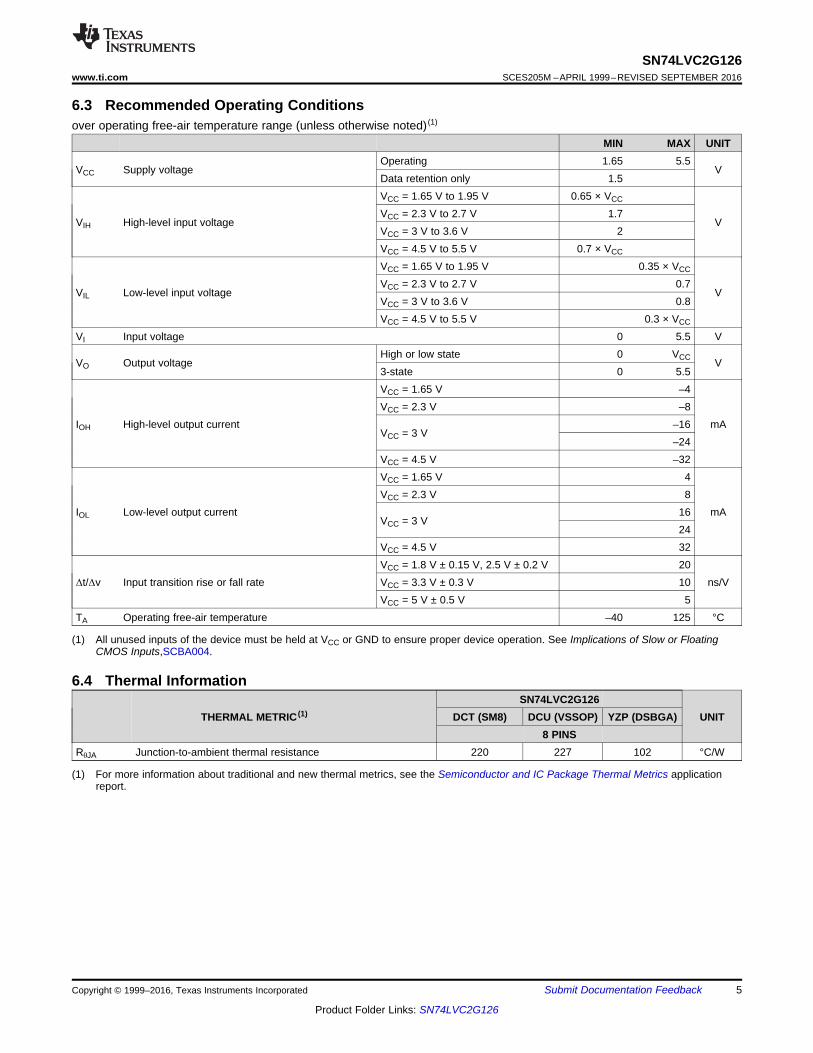
(1) All unused inputs of the device must be held at VCC or GND to ensure proper device operation. See Implications of Slow or FloatingCMOS Inputs,SCBA004.
6.3 Recommended Operating Conditionsover operating free-air temperature range (unless otherwise noted) (1)
MIN MAX UNIT
VCC Supply voltageOperating 1.65 5.5
VData retention only 1.5
VIH High-level input voltage
VCC = 1.65 V to 1.95 V 0.65 × VCC
VVCC = 2.3 V to 2.7 V 1.7VCC = 3 V to 3.6 V 2VCC = 4.5 V to 5.5 V 0.7 × VCC
VIL Low-level input voltage
VCC = 1.65 V to 1.95 V 0.35 × VCC
VVCC = 2.3 V to 2.7 V 0.7VCC = 3 V to 3.6 V 0.8VCC = 4.5 V to 5.5 V 0.3 × VCC
VI Input voltage 0 5.5 V
VO Output voltageHigh or low state 0 VCC V3-state 0 5.5
IOH High-level output current
VCC = 1.65 V –4
mAVCC = 2.3 V –8
VCC = 3 V–16–24
VCC = 4.5 V –32
IOL Low-level output current
VCC = 1.65 V 4
mAVCC = 2.3 V 8
VCC = 3 V1624
VCC = 4.5 V 32
Δt/Δv Input transition rise or fall rateVCC = 1.8 V ± 0.15 V, 2.5 V ± 0.2 V 20
ns/VVCC = 3.3 V ± 0.3 V 10VCC = 5 V ± 0.5 V 5
TA Operating free-air temperature –40 125 °C
(1) For more information about traditional and new thermal metrics, see the Semiconductor and IC Package Thermal Metrics applicationreport.
6.4 Thermal Information
THERMAL METRIC (1)SN74LVC2G126
UNITDCT (SM8) DCU (VSSOP) YZP (DSBGA)8 PINS
RθJA Junction-to-ambient thermal resistance 220 227 102 °C/W

6
SN74LVC2G126SCES205M –APRIL 1999–REVISED SEPTEMBER 2016 www.ti.com
Product Folder Links: SN74LVC2G126
Submit Documentation Feedback Copyright © 1999–2016, Texas Instruments Incorporated
(1) All typical values are at VCC = 3.3 V, TA = 25°C.
6.5 Electrical Characteristicsover recommended operating free-air temperature range (unless otherwise noted)
PARAMETER TEST CONDITIONS VCCTA = 25°C –40°C to +85°C –40°C to +125°C
UNITMIN TYP (1) MAX MIN MAX MIN MAX
VOH
IOH = –100 µA 1.65 V to5.5 V VCC – 0.1 VCC – 0.1 VCC – 0.1
V
IOH = –4 mA 1.65 V 1.2 1.2 1.2
IOH = –8 mA 2.3 V 1.9 1.9 1.9
IOH = –16 mA3 V
2.4 2.4 2.4
IOH = –24 mA 2.3 2.3 2.3
IOH = –32 mA 4.5 V 3.8 3.8 3.8
VOL
IOL = 100 µA 1.65 V to5.5 V 0.1 0.1 0.1
V
IOL = 4 mA 1.65 V 0.45 0.45 0.45
IOL = 8 mA 2.3 V 0.3 0.3 0.3
IOL = 16 mA3 V
0.4 0.4 0.4
IOL = 24 mA 0.55 0.55 0.55
IOL = 32 mA 4.5 V 0.55 0.55 0.75
IIA or OEinputs VI = 5.5 V or GND 0 to
5.5 V ±5 ±5 ±5 µA
Ioff VI or VO = 5.5 V 0 ±10 ±10 ±10 µA
IOZ VO = 0 to 5.5 V 3.6 V 10 10 10 µA
ICC VI = 5.5 V or GND IO = 0 1.65 V to5.5 V 10 10 10 µA
ΔICCOne input at VCC – 0.6 V,Other inputs at VCC or GND
3 V to5.5 V 500 500 500 µA
CI
Datainputs
VI = VCC or GND 3.3 V3.5
pFControlinputs 4
Co VO = VCC or GND 3.3 V 6.5 pF
6.6 Switching Characteristics, –40°C to +85°Cover recommended operating free-air temperature range (unless otherwise noted) (see Figure 3)
PARAMETER FROM(INPUT)
TO(OUTPUT)
–40°C to +85°C
UNITVCC = 1.8 V± 0.15 V
VCC = 2.5 V± 0.2 V
VCC = 3.3 V± 0.3 V
VCC = 5 V± 0.5 V
MIN MAX MIN MAX MIN MAX MIN MAX
tpd A Y 3.5 9.8 1.7 4.9 1.4 4 1 3.2 ns
ten OE Y 3.5 10 1.7 5 1.5 4.1 1 3.1 ns
tdis OE Y 1.7 12.6 1 5.7 1 4.4 1 3.3 ns
6.7 Switching Characteristics, –40°C to +125°Cover recommended operating free-air temperature range (unless otherwise noted) (see Figure 3)
PARAMETER FROM(INPUT)
TO(OUTPUT)
–40°C to +125°C
UNITVCC = 1.8 V± 0.15 V
VCC = 2.5 V± 0.2 V
VCC = 3.3 V± 0.3 V
VCC = 5 V± 0.5 V
MIN MAX MIN MAX MIN MAX MIN MAX
tpd A Y 3.5 10.8 1.7 5.9 1.4 5 1 3.7 ns
ten OE Y 3.5 11 1.7 6 1.5 5.1 1 3.6 ns
tdis OE Y 1.7 13.6 1 6.7 1 5.4 1 3.8 ns

Temperature - °C
TP
D -
ns
-100 -50 0 50 100 1500
0.5
1
1.5
2
2.5
D001
TPD
V - VCC
TP
D -
ns
0 1 2 3 4 5 6
0
1
2
3
4
5
D002
TPDTPD
7
SN74LVC2G126www.ti.com SCES205M –APRIL 1999–REVISED SEPTEMBER 2016
Product Folder Links: SN74LVC2G126
Submit Documentation FeedbackCopyright © 1999–2016, Texas Instruments Incorporated
6.8 Operating CharacteristicsTA = 25°
PARAMETER TESTCONDITIONS
VCC = 1.8 V VCC = 2.5 V VCC = 3.3 V VCC = 5 VUNIT
TYP TYP TYP TYP
CpdPower dissipationcapacitance
Outputs enabledf = 10 MHz
19 19 20 22pF
Outputs disabled 2 2 2 3
6.9 Typical Characteristics
Figure 1. TPD Across Tempearture at 3.3 VCC Figure 2. TPD Across VCC at 25°C
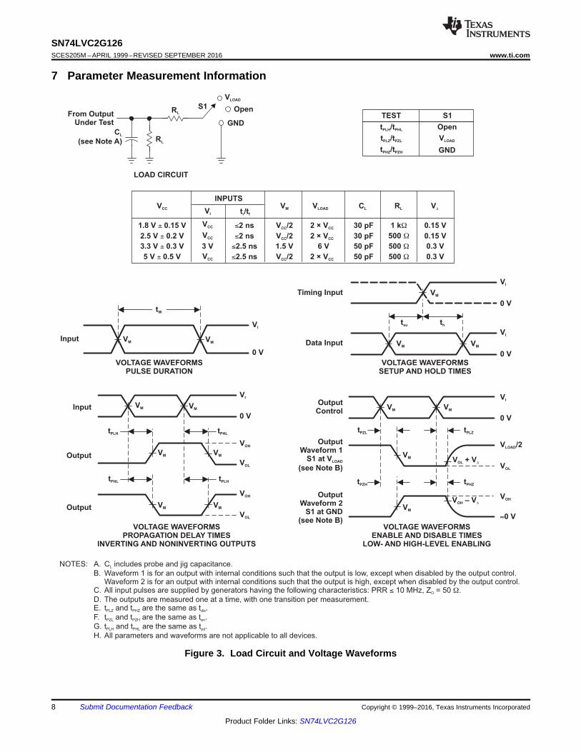
thtsu
From OutputUnder Test
C
(see Note A)L
LOAD CIRCUIT
S1
VLOAD
Open
GND
RL
Data Input
Timing Input
0 V
0 V0 V
tW
Input
0 VInput
OutputWaveform 1
S1 at V
(see Note B)LOAD
OutputWaveform 2
S1 at GND(see Note B)
VOL
VOH
0 V
»0 V
Output
Output
TEST S1
t /tPLH PHL Open
OutputControl
VM
VM VM
VM
VM
1.8 V 0.15 V±
2.5 V 0.2 V±
3.3 V 0.3 V±
5 V 0.5 V±
1 kW
500 W
500 W
500 W
VCC RL
2 × VCC
2 × VCC
6 V
2 × VCC
VLOAD CL
30 pF
30 pF
50 pF
50 pF
0.15 V
0.15 V
0.3 V
0.3 V
VD
3 V
VI
VCC/2
VCC/2
1.5 V
VCC/2
VM
£2 ns
£2 ns
£2.5 ns
£2.5 ns
INPUTS
RL
t /tr f
VCC
VCC
VCC
VLOADt /tPLZ PZL
GNDt /tPHZ PZH
VOLTAGE WAVEFORMSENABLE AND DISABLE TIMES
LOW- AND HIGH-LEVEL ENABLING
VOLTAGE WAVEFORMSPROPAGATION DELAY TIMES
INVERTING AND NONINVERTING OUTPUTS
NOTES: A. C includes probe and jig capacitance.
B. Waveform 1 is for an output with internal conditions such that the output is low, except when disabled by the output control.Waveform 2 is for an output with internal conditions such that the output is high, except when disabled by the output control.
C. All input pulses are supplied by generators having the following characteristics: PRR 10 MHz, Z = 50 .
D. The outputs are measured one at a time, with one transition per measurement.E. t and t are the same as t .
F. t and t are the same as t .
G. t and t are the same as t .
H. All parameters and waveforms are not applicable to all devices.
L
O
PLZ PHZ dis
PZL PZH en
PLH PHL pd
£ W
VOLTAGE WAVEFORMSPULSE DURATION
VOLTAGE WAVEFORMSSETUP AND HOLD TIMES
VI
VI
VI
VM
VM
V /2LOAD
tPZL tPLZ
tPHZtPZH
V – VOH D
V + VOL D
VM
VM VM
VM
VOL
VOH
VI
VI
VOH
VOL
VM
VM
VM
VM
tPLH tPHL
tPLHtPHL
8
SN74LVC2G126SCES205M –APRIL 1999–REVISED SEPTEMBER 2016 www.ti.com
Product Folder Links: SN74LVC2G126
Submit Documentation Feedback Copyright © 1999–2016, Texas Instruments Incorporated
7 Parameter Measurement Information
Figure 3. Load Circuit and Voltage Waveforms

1A 1Y
1OE
2A
2OE
2Y
9
SN74LVC2G126www.ti.com SCES205M –APRIL 1999–REVISED SEPTEMBER 2016
Product Folder Links: SN74LVC2G126
Submit Documentation FeedbackCopyright © 1999–2016, Texas Instruments Incorporated
8 Detailed Description
8.1 OverviewThe SN74LVC2G126 device contains a dual buffer gate with output enable control and performs the Booleanfunction Y = A.
This device is fully specified for partial-power-down applications using Ioff. The Ioff circuitry disables the outputs,preventing damaging current backflow through the device when it is powered down.
To ensure the high-impedance state during power up or power down, OE should be tied to VCC through apulldown resistor; the minimum value of the resistor is determined by the current-sourcing capability of the driver.
8.2 Functional Block Diagram
8.3 Feature Description• 1.65 V to 5.5 V operating voltage range• Allows down voltage translation
– 5 V to 3.3 V– 5 V or 3.3 V to 1.8V
• Inputs accept voltages to 5.5 V– 5-V tolerance on input pin
• Ioff feature– Allows voltage on the inputs and outputs when VCC is 0 V– Able to prevent leakage when VCC is 0 V
8.4 Device Functional ModesTable 1 lists the functional modes of SN74LVC2G126.
Table 1. Function TableINPUTS OUTPUT
YOE AH H HH L LL X Z
uC or Logic
Basic LED Driver
Wired OR
uC or Logic
Buffer Function
uC or Logic
VCC
uC or Logic
VCC
uC or Logic
10
SN74LVC2G126SCES205M –APRIL 1999–REVISED SEPTEMBER 2016 www.ti.com
Product Folder Links: SN74LVC2G126
Submit Documentation Feedback Copyright © 1999–2016, Texas Instruments Incorporated
9 Application and Implementation
NOTEInformation in the following applications sections is not part of the TI componentspecification, and TI does not warrant its accuracy or completeness. TI’s customers areresponsible for determining suitability of components for their purposes. Customers shouldvalidate and test their design implementation to confirm system functionality.
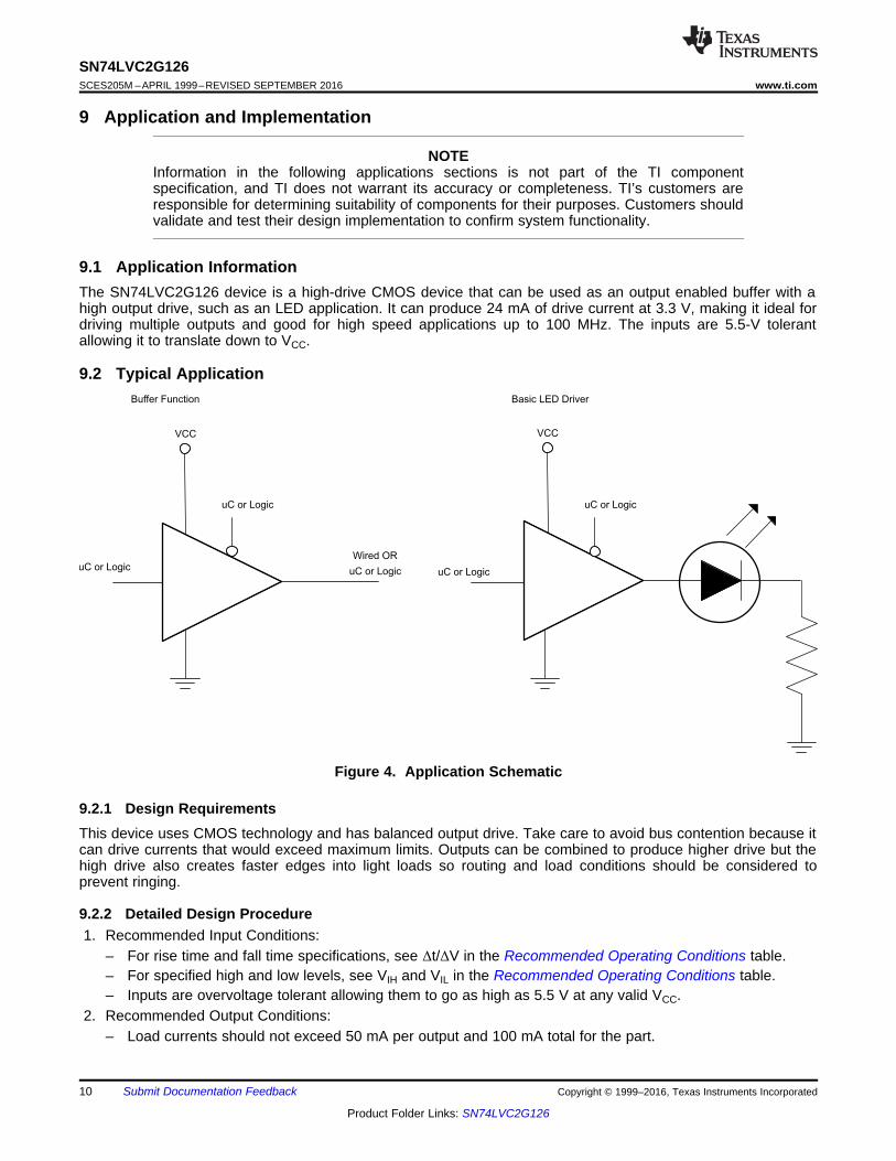
9.1 Application InformationThe SN74LVC2G126 device is a high-drive CMOS device that can be used as an output enabled buffer with ahigh output drive, such as an LED application. It can produce 24 mA of drive current at 3.3 V, making it ideal fordriving multiple outputs and good for high speed applications up to 100 MHz. The inputs are 5.5-V tolerantallowing it to translate down to VCC.
9.2 Typical Application
Figure 4. Application Schematic
9.2.1 Design RequirementsThis device uses CMOS technology and has balanced output drive. Take care to avoid bus contention because itcan drive currents that would exceed maximum limits. Outputs can be combined to produce higher drive but thehigh drive also creates faster edges into light loads so routing and load conditions should be considered toprevent ringing.
9.2.2 Detailed Design Procedure1. Recommended Input Conditions:
– For rise time and fall time specifications, see Δt/ΔV in the Recommended Operating Conditions table.– For specified high and low levels, see VIH and VIL in the Recommended Operating Conditions table.– Inputs are overvoltage tolerant allowing them to go as high as 5.5 V at any valid VCC.
2. Recommended Output Conditions:– Load currents should not exceed 50 mA per output and 100 mA total for the part.
Vcc
Unused Input
Input
Output
Input
Unused Input Output
Frequency (MHz)
I(m
A)
CC
0 20 40 60 800
1
2
3
4
5
6
7
8
9
10
D003
V 1.8 VCCVCC 2.5 VVCC 3.3 VVCC 5 V
11
SN74LVC2G126www.ti.com SCES205M –APRIL 1999–REVISED SEPTEMBER 2016
Product Folder Links: SN74LVC2G126
Submit Documentation FeedbackCopyright © 1999–2016, Texas Instruments Incorporated
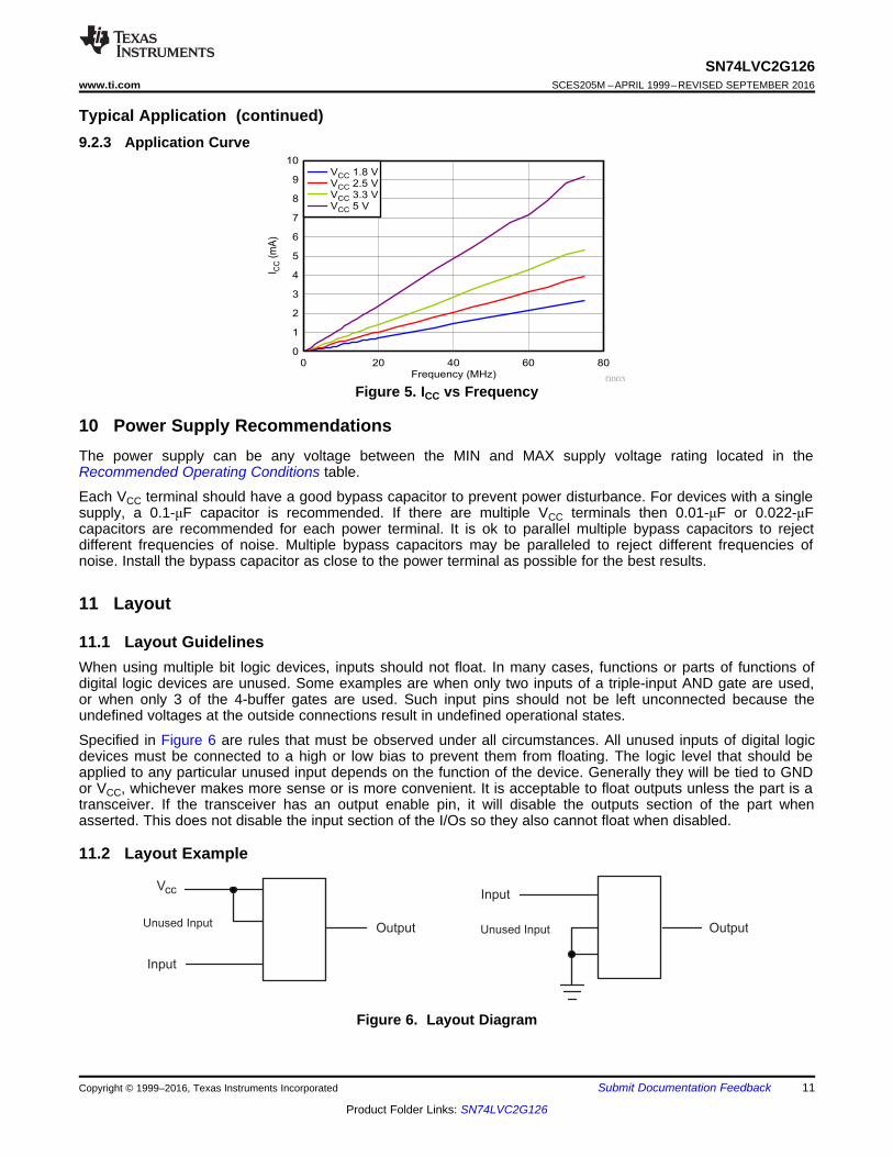
Typical Application (continued)9.2.3 Application Curve
Figure 5. ICC vs Frequency
10 Power Supply RecommendationsThe power supply can be any voltage between the MIN and MAX supply voltage rating located in theRecommended Operating Conditions table.
Each VCC terminal should have a good bypass capacitor to prevent power disturbance. For devices with a singlesupply, a 0.1-μF capacitor is recommended. If there are multiple VCC terminals then 0.01-μF or 0.022-μFcapacitors are recommended for each power terminal. It is ok to parallel multiple bypass capacitors to rejectdifferent frequencies of noise. Multiple bypass capacitors may be paralleled to reject different frequencies ofnoise. Install the bypass capacitor as close to the power terminal as possible for the best results.
11 Layout
11.1 Layout GuidelinesWhen using multiple bit logic devices, inputs should not float. In many cases, functions or parts of functions ofdigital logic devices are unused. Some examples are when only two inputs of a triple-input AND gate are used,or when only 3 of the 4-buffer gates are used. Such input pins should not be left unconnected because theundefined voltages at the outside connections result in undefined operational states.
Specified in Figure 6 are rules that must be observed under all circumstances. All unused inputs of digital logicdevices must be connected to a high or low bias to prevent them from floating. The logic level that should beapplied to any particular unused input depends on the function of the device. Generally they will be tied to GNDor VCC, whichever makes more sense or is more convenient. It is acceptable to float outputs unless the part is atransceiver. If the transceiver has an output enable pin, it will disable the outputs section of the part whenasserted. This does not disable the input section of the I/Os so they also cannot float when disabled.
11.2 Layout Example
Figure 6. Layout Diagram
12
SN74LVC2G126SCES205M –APRIL 1999–REVISED SEPTEMBER 2016 www.ti.com
Product Folder Links: SN74LVC2G126
Submit Documentation Feedback Copyright © 1999–2016, Texas Instruments Incorporated
12 Device and Documentation Support
12.1 Receiving Notification of Documentation UpdatesTo receive notification of documentation updates, navigate to the device product folder on ti.com. In the upperright corner, click on Alert me to register and receive a weekly digest of any product information that haschanged. For change details, review the revision history included in any revised document.
12.2 Community ResourcesThe following links connect to TI community resources. Linked contents are provided "AS IS" by the respectivecontributors. They do not constitute TI specifications and do not necessarily reflect TI's views; see TI's Terms ofUse.
TI E2E™ Online Community TI's Engineer-to-Engineer (E2E) Community. Created to foster collaborationamong engineers. At e2e.ti.com, you can ask questions, share knowledge, explore ideas and helpsolve problems with fellow engineers.
Design Support TI's Design Support Quickly find helpful E2E forums along with design support tools andcontact information for technical support.
12.3 TrademarksE2E is a trademark of Texas Instruments.All other trademarks are the property of their respective owners.
12.4 Electrostatic Discharge CautionThese devices have limited built-in ESD protection. The leads should be shorted together or the device placed in conductive foamduring storage or handling to prevent electrostatic damage to the MOS gates.
12.5 GlossarySLYZ022 — TI Glossary.
This glossary lists and explains terms, acronyms, and definitions.
13 Mechanical, Packaging, and Orderable InformationThe following pages include mechanical packaging and orderable information. This information is the mostcurrent data available for the designated devices. This data is subject to change without notice and revision ofthis document. For browser based versions of this data sheet, refer to the left hand navigation.

PACKAGE OPTION ADDENDUM
www.ti.com 15-Apr-2017
Addendum-Page 1
PACKAGING INFORMATION
Orderable Device Status(1)
Package Type PackageDrawing
Pins PackageQty
Eco Plan(2)
Lead/Ball Finish(6)
MSL Peak Temp(3)
Op Temp (°C) Device Marking(4/5)
Samples
74LVC2G126DCTRG4 ACTIVE SM8 DCT 8 3000 Green (RoHS& no Sb/Br)
CU NIPDAU Level-1-260C-UNLIM -40 to 125 C26Z
74LVC2G126DCUTG4 ACTIVE VSSOP DCU 8 250 Green (RoHS& no Sb/Br)
CU NIPDAU Level-1-260C-UNLIM -40 to 125 C26R
SN74LVC2G126DCTR ACTIVE SM8 DCT 8 3000 Green (RoHS& no Sb/Br)
CU NIPDAU Level-1-260C-UNLIM -40 to 125 C26Z
SN74LVC2G126DCUR ACTIVE VSSOP DCU 8 3000 Green (RoHS& no Sb/Br)
CU NIPDAU | CU SN Level-1-260C-UNLIM -40 to 125 (C26Q ~ C26R)
SN74LVC2G126DCUT ACTIVE VSSOP DCU 8 250 Green (RoHS& no Sb/Br)
CU NIPDAU | CU SN Level-1-260C-UNLIM -40 to 125 (C26Q ~ C26R)
SN74LVC2G126YZPR ACTIVE DSBGA YZP 8 3000 Green (RoHS& no Sb/Br)
SNAGCU Level-1-260C-UNLIM -40 to 125 (CN7 ~ CNN)
(1) The marketing status values are defined as follows:ACTIVE: Product device recommended for new designs.LIFEBUY: TI has announced that the device will be discontinued, and a lifetime-buy period is in effect.NRND: Not recommended for new designs. Device is in production to support existing customers, but TI does not recommend using this part in a new design.PREVIEW: Device has been announced but is not in production. Samples may or may not be available.OBSOLETE: TI has discontinued the production of the device.
(2) Eco Plan - The planned eco-friendly classification: Pb-Free (RoHS), Pb-Free (RoHS Exempt), or Green (RoHS & no Sb/Br) - please check http://www.ti.com/productcontent for the latest availabilityinformation and additional product content details.TBD: The Pb-Free/Green conversion plan has not been defined.Pb-Free (RoHS): TI's terms "Lead-Free" or "Pb-Free" mean semiconductor products that are compatible with the current RoHS requirements for all 6 substances, including the requirement thatlead not exceed 0.1% by weight in homogeneous materials. Where designed to be soldered at high temperatures, TI Pb-Free products are suitable for use in specified lead-free processes.Pb-Free (RoHS Exempt): This component has a RoHS exemption for either 1) lead-based flip-chip solder bumps used between the die and package, or 2) lead-based die adhesive used betweenthe die and leadframe. The component is otherwise considered Pb-Free (RoHS compatible) as defined above.Green (RoHS & no Sb/Br): TI defines "Green" to mean Pb-Free (RoHS compatible), and free of Bromine (Br) and Antimony (Sb) based flame retardants (Br or Sb do not exceed 0.1% by weightin homogeneous material)
(3) MSL, Peak Temp. - The Moisture Sensitivity Level rating according to the JEDEC industry standard classifications, and peak solder temperature.
(4) There may be additional marking, which relates to the logo, the lot trace code information, or the environmental category on the device.
(5) Multiple Device Markings will be inside parentheses. Only one Device Marking contained in parentheses and separated by a "~" will appear on a device. If a line is indented then it is a continuationof the previous line and the two combined represent the entire Device Marking for that device.

PACKAGE OPTION ADDENDUM
www.ti.com 15-Apr-2017
Addendum-Page 2
(6) Lead/Ball Finish - Orderable Devices may have multiple material finish options. Finish options are separated by a vertical ruled line. Lead/Ball Finish values may wrap to two lines if the finishvalue exceeds the maximum column width.
Important Information and Disclaimer:The information provided on this page represents TI's knowledge and belief as of the date that it is provided. TI bases its knowledge and belief on informationprovided by third parties, and makes no representation or warranty as to the accuracy of such information. Efforts are underway to better integrate information from third parties. TI has taken andcontinues to take reasonable steps to provide representative and accurate information but may not have conducted destructive testing or chemical analysis on incoming materials and chemicals.TI and TI suppliers consider certain information to be proprietary, and thus CAS numbers and other limited information may not be available for release.
In no event shall TI's liability arising out of such information exceed the total purchase price of the TI part(s) at issue in this document sold by TI to Customer on an annual basis.
OTHER QUALIFIED VERSIONS OF SN74LVC2G126 :
• Enhanced Product: SN74LVC2G126-EP
NOTE: Qualified Version Definitions:
• Enhanced Product - Supports Defense, Aerospace and Medical Applications

TAPE AND REEL INFORMATION
*All dimensions are nominal
Device PackageType
PackageDrawing
Pins SPQ ReelDiameter
(mm)
ReelWidth
W1 (mm)
A0(mm)
B0(mm)
K0(mm)
P1(mm)
W(mm)
Pin1Quadrant
74LVC2G126DCUTG4 VSSOP DCU 8 250 180.0 8.4 2.25 3.35 1.05 4.0 8.0 Q3
SN74LVC2G126DCTR SM8 DCT 8 3000 180.0 13.0 3.35 4.5 1.55 4.0 12.0 Q3
SN74LVC2G126DCUR VSSOP DCU 8 3000 180.0 8.4 2.25 3.35 1.05 4.0 8.0 Q3
SN74LVC2G126DCUR VSSOP DCU 8 3000 178.0 9.5 2.25 3.35 1.05 4.0 8.0 Q3
SN74LVC2G126YZPR DSBGA YZP 8 3000 178.0 9.2 1.02 2.02 0.63 4.0 8.0 Q1
PACKAGE MATERIALS INFORMATION
www.ti.com 29-Sep-2017
Pack Materials-Page 1
*All dimensions are nominal
Device Package Type Package Drawing Pins SPQ Length (mm) Width (mm) Height (mm)
74LVC2G126DCUTG4 VSSOP DCU 8 250 202.0 201.0 28.0
SN74LVC2G126DCTR SM8 DCT 8 3000 182.0 182.0 20.0
SN74LVC2G126DCUR VSSOP DCU 8 3000 202.0 201.0 28.0
SN74LVC2G126DCUR VSSOP DCU 8 3000 202.0 201.0 28.0
SN74LVC2G126YZPR DSBGA YZP 8 3000 220.0 220.0 35.0
PACKAGE MATERIALS INFORMATION
www.ti.com 29-Sep-2017
Pack Materials-Page 2
MECHANICAL DATA
MPDS049B – MAY 1999 – REVISED OCTOBER 2002
POST OFFICE BOX 655303 • DALLAS, TEXAS 75265
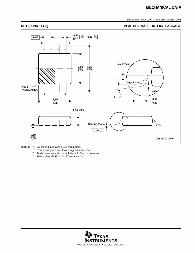
DCT (R-PDSO-G8) PLASTIC SMALL-OUTLINE PACKAGE
ÇÇÇÇÇÇÇÇÇÇÇÇÇÇÇÇÇÇÇÇ
0,600,20
0,25
0° – 8°
0,15 NOM
Gage Plane
4188781/C 09/02
4,25
5
0,300,15
2,903,752,70
8
4
3,152,75
1
0,100,00
1,30 MAX
Seating Plane
0,10
M0,130,65
PIN 1INDEX AREA
NOTES: A. All linear dimensions are in millimeters.B. This drawing is subject to change without notice.C. Body dimensions do not include mold flash or protrusionD. Falls within JEDEC MO-187 variation DA.


www.ti.com
PACKAGE OUTLINE
C0.5 MAX
0.190.15
1.5TYP
0.5 TYP
8X 0.250.21
0.5TYP
B E A
D
4223082/A 07/2016
DSBGA - 0.5 mm max heightYZP0008DIE SIZE BALL GRID ARRAY
NOTES: 1. All linear dimensions are in millimeters. Any dimensions in parenthesis are for reference only. Dimensioning and tolerancing per ASME Y14.5M.2. This drawing is subject to change without notice.
BALL A1CORNER
SEATING PLANE
BALL TYP0.05 C
B
1 2
0.015 C A B
SYMM
SYMM
C
A
D
SCALE 8.000
D: Max =
E: Max =
1.918 mm, Min =
0.918 mm, Min =
1.858 mm
0.858 mm

www.ti.com
EXAMPLE BOARD LAYOUT
8X ( 0.23)(0.5) TYP
(0.5) TYP
( 0.23)METAL
0.05 MAX ( 0.23)SOLDER MASKOPENING
0.05 MIN
4223082/A 07/2016
DSBGA - 0.5 mm max heightYZP0008DIE SIZE BALL GRID ARRAY
NOTES: (continued) 3. Final dimensions may vary due to manufacturing tolerance considerations and also routing constraints. For more information, see Texas Instruments literature number SNVA009 (www.ti.com/lit/snva009).
SYMM
SYMM
LAND PATTERN EXAMPLESCALE:40X
1 2
A
B
C
D
NON-SOLDER MASKDEFINED
(PREFERRED)
SOLDER MASK DETAILSNOT TO SCALE
SOLDER MASKOPENING
SOLDER MASKDEFINED
METAL UNDERSOLDER MASK
www.ti.com
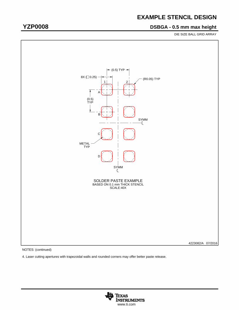
EXAMPLE STENCIL DESIGN
(0.5)TYP
(0.5) TYP
8X ( 0.25) (R0.05) TYP
METALTYP
4223082/A 07/2016
DSBGA - 0.5 mm max heightYZP0008DIE SIZE BALL GRID ARRAY
NOTES: (continued) 4. Laser cutting apertures with trapezoidal walls and rounded corners may offer better paste release.
SYMM
SYMM
SOLDER PASTE EXAMPLEBASED ON 0.1 mm THICK STENCIL
SCALE:40X
1 2
A
B
C
D


IMPORTANT NOTICE
Texas Instruments Incorporated (TI) reserves the right to make corrections, enhancements, improvements and other changes to itssemiconductor products and services per JESD46, latest issue, and to discontinue any product or service per JESD48, latest issue. Buyersshould obtain the latest relevant information before placing orders and should verify that such information is current and complete.TI’s published terms of sale for semiconductor products (http://www.ti.com/sc/docs/stdterms.htm) apply to the sale of packaged integratedcircuit products that TI has qualified and released to market. Additional terms may apply to the use or sale of other types of TI products andservices.Reproduction of significant portions of TI information in TI data sheets is permissible only if reproduction is without alteration and isaccompanied by all associated warranties, conditions, limitations, and notices. TI is not responsible or liable for such reproduceddocumentation. Information of third parties may be subject to additional restrictions. Resale of TI products or services with statementsdifferent from or beyond the parameters stated by TI for that product or service voids all express and any implied warranties for theassociated TI product or service and is an unfair and deceptive business practice. TI is not responsible or liable for any such statements.Buyers and others who are developing systems that incorporate TI products (collectively, “Designers”) understand and agree that Designersremain responsible for using their independent analysis, evaluation and judgment in designing their applications and that Designers havefull and exclusive responsibility to assure the safety of Designers' applications and compliance of their applications (and of all TI productsused in or for Designers’ applications) with all applicable regulations, laws and other applicable requirements. Designer represents that, withrespect to their applications, Designer has all the necessary expertise to create and implement safeguards that (1) anticipate dangerousconsequences of failures, (2) monitor failures and their consequences, and (3) lessen the likelihood of failures that might cause harm andtake appropriate actions. Designer agrees that prior to using or distributing any applications that include TI products, Designer willthoroughly test such applications and the functionality of such TI products as used in such applications.TI’s provision of technical, application or other design advice, quality characterization, reliability data or other services or information,including, but not limited to, reference designs and materials relating to evaluation modules, (collectively, “TI Resources”) are intended toassist designers who are developing applications that incorporate TI products; by downloading, accessing or using TI Resources in anyway, Designer (individually or, if Designer is acting on behalf of a company, Designer’s company) agrees to use any particular TI Resourcesolely for this purpose and subject to the terms of this Notice.TI’s provision of TI Resources does not expand or otherwise alter TI’s applicable published warranties or warranty disclaimers for TIproducts, and no additional obligations or liabilities arise from TI providing such TI Resources. TI reserves the right to make corrections,enhancements, improvements and other changes to its TI Resources. TI has not conducted any testing other than that specificallydescribed in the published documentation for a particular TI Resource.Designer is authorized to use, copy and modify any individual TI Resource only in connection with the development of applications thatinclude the TI product(s) identified in such TI Resource. NO OTHER LICENSE, EXPRESS OR IMPLIED, BY ESTOPPEL OR OTHERWISETO ANY OTHER TI INTELLECTUAL PROPERTY RIGHT, AND NO LICENSE TO ANY TECHNOLOGY OR INTELLECTUAL PROPERTYRIGHT OF TI OR ANY THIRD PARTY IS GRANTED HEREIN, including but not limited to any patent right, copyright, mask work right, orother intellectual property right relating to any combination, machine, or process in which TI products or services are used. Informationregarding or referencing third-party products or services does not constitute a license to use such products or services, or a warranty orendorsement thereof. Use of TI Resources may require a license from a third party under the patents or other intellectual property of thethird party, or a license from TI under the patents or other intellectual property of TI.TI RESOURCES ARE PROVIDED “AS IS” AND WITH ALL FAULTS. TI DISCLAIMS ALL OTHER WARRANTIES ORREPRESENTATIONS, EXPRESS OR IMPLIED, REGARDING RESOURCES OR USE THEREOF, INCLUDING BUT NOT LIMITED TOACCURACY OR COMPLETENESS, TITLE, ANY EPIDEMIC FAILURE WARRANTY AND ANY IMPLIED WARRANTIES OFMERCHANTABILITY, FITNESS FOR A PARTICULAR PURPOSE, AND NON-INFRINGEMENT OF ANY THIRD PARTY INTELLECTUALPROPERTY RIGHTS. TI SHALL NOT BE LIABLE FOR AND SHALL NOT DEFEND OR INDEMNIFY DESIGNER AGAINST ANY CLAIM,INCLUDING BUT NOT LIMITED TO ANY INFRINGEMENT CLAIM THAT RELATES TO OR IS BASED ON ANY COMBINATION OFPRODUCTS EVEN IF DESCRIBED IN TI RESOURCES OR OTHERWISE. IN NO EVENT SHALL TI BE LIABLE FOR ANY ACTUAL,DIRECT, SPECIAL, COLLATERAL, INDIRECT, PUNITIVE, INCIDENTAL, CONSEQUENTIAL OR EXEMPLARY DAMAGES INCONNECTION WITH OR ARISING OUT OF TI RESOURCES OR USE THEREOF, AND REGARDLESS OF WHETHER TI HAS BEENADVISED OF THE POSSIBILITY OF SUCH DAMAGES.Unless TI has explicitly designated an individual product as meeting the requirements of a particular industry standard (e.g., ISO/TS 16949and ISO 26262), TI is not responsible for any failure to meet such industry standard requirements.Where TI specifically promotes products as facilitating functional safety or as compliant with industry functional safety standards, suchproducts are intended to help enable customers to design and create their own applications that meet applicable functional safety standardsand requirements. Using products in an application does not by itself establish any safety features in the application. Designers mustensure compliance with safety-related requirements and standards applicable to their applications. Designer may not use any TI products inlife-critical medical equipment unless authorized officers of the parties have executed a special contract specifically governing such use.Life-critical medical equipment is medical equipment where failure of such equipment would cause serious bodily injury or death (e.g., lifesupport, pacemakers, defibrillators, heart pumps, neurostimulators, and implantables). Such equipment includes, without limitation, allmedical devices identified by the U.S. Food and Drug Administration as Class III devices and equivalent classifications outside the U.S.TI may expressly designate certain products as completing a particular qualification (e.g., Q100, Military Grade, or Enhanced Product).Designers agree that it has the necessary expertise to select the product with the appropriate qualification designation for their applicationsand that proper product selection is at Designers’ own risk. Designers are solely responsible for compliance with all legal and regulatoryrequirements in connection with such selection.Designer will fully indemnify TI and its representatives against any damages, costs, losses, and/or liabilities arising out of Designer’s non-compliance with the terms and provisions of this Notice.
Mailing Address: Texas Instruments, Post Office Box 655303, Dallas, Texas 75265Copyright © 2017, Texas Instruments Incorporated