sn74aup1g08 low-power single 2-input - texas instruments
TRANSCRIPT
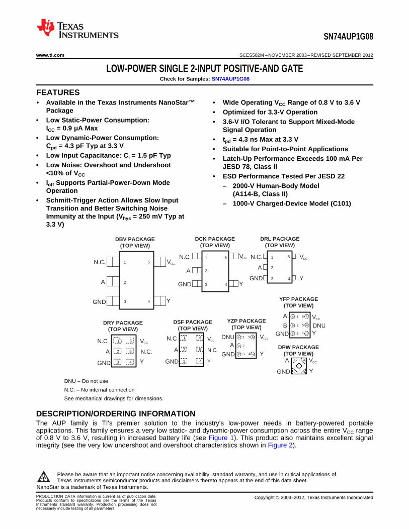
N.C. 1
A 2
GND 3
5 VCC
4 Y
N.C. 1
A 2
GND 3
5 VCC
4 Y
N.C. 1
A 2
GND 3
5 VCC
4 Y
N.C. 1
6 VCC
N.C . 1
6 VCC
DNU
A1 1
5 A2
VCC
A 2 5
N.C. A 2 5 N.C. A
GND B1 2
C1 3
4 C2 Y
GND 3 4 Y GND 3 4 Y
YZP PACKAGE (TOP VIEW)
YFP PACKAGE (TOP VIEW)
DSF PACKAGE (TOP VIEW)
DRY PACKAGE (TOP VIEW)
DBV PACKAGE (TOP VIEW)
DCK PACKAGE (TOP VIEW)
DRL PACKAGE (TOP VIEW)
DNU
A1 1 6 A2 A
GND B1 2
C1 3
4 C2 Y
A25BVCC
1 4
2 3
A
GND Y
VCC
DPW PACKAGE (TOP VIEW)
SN74AUP1G08
www.ti.com SCES502M –NOVEMBER 2003–REVISED SEPTEMBER 2012
LOW-POWER SINGLE 2-INPUT POSITIVE-AND GATECheck for Samples: SN74AUP1G08
1FEATURES2• Available in the Texas Instruments NanoStar™ • Wide Operating VCC Range of 0.8 V to 3.6 V
Package • Optimized for 3.3-V Operation• Low Static-Power Consumption: • 3.6-V I/O Tolerant to Support Mixed-Mode
ICC = 0.9 μA Max Signal Operation• Low Dynamic-Power Consumption: • tpd = 4.3 ns Max at 3.3 V
Cpd = 4.3 pF Typ at 3.3 V • Suitable for Point-to-Point Applications• Low Input Capacitance: Ci = 1.5 pF Typ • Latch-Up Performance Exceeds 100 mA Per• Low Noise: Overshoot and Undershoot JESD 78, Class II
<10% of VCC • ESD Performance Tested Per JESD 22• Ioff Supports Partial-Power-Down Mode – 2000-V Human-Body Model
Operation (A114-B, Class II)• Schmitt-Trigger Action Allows Slow Input – 1000-V Charged-Device Model (C101)
Transition and Better Switching NoiseImmunity at the Input (Vhys = 250 mV Typ at3.3 V)
DNU – Do not use
N.C. – No internal connection
See mechanical drawings for dimensions.
DESCRIPTION/ORDERING INFORMATIONThe AUP family is TI's premier solution to the industry's low-power needs in battery-powered portableapplications. This family ensures a very low static- and dynamic-power consumption across the entire VCC rangeof 0.8 V to 3.6 V, resulting in increased battery life (see Figure 1). This product also maintains excellent signalintegrity (see the very low undershoot and overshoot characteristics shown in Figure 2).
1
Please be aware that an important notice concerning availability, standard warranty, and use in critical applications ofTexas Instruments semiconductor products and disclaimers thereto appears at the end of this data sheet.
2NanoStar is a trademark of Texas Instruments.
PRODUCTION DATA information is current as of publication date. Copyright © 2003–2012, Texas Instruments IncorporatedProducts conform to specifications per the terms of the TexasInstruments standard warranty. Production processing does notnecessarily include testing of all parameters.

1
24A
BY
Y A • B or Y A B
−0.50
0.5
11.5
2
2.5
3
3.5
0 5 10 15 20 25 30 35 40 45Time − ns
Vol
tage
− V
† AUP1G08 data at CL = 15 pF
OutputInput
Switching Characteristics
at 25 MHz†
AUP
LVC
AUPAUP
LVC
Static-Power Consumption
(µA)
Dynamic-Power Consumption
(pF)
† Single, dual, and triple gates
3.3-VLogic †
3.3-VLogic †
0%
20%
40%
60%
80%
100%
0%
20%
40%
60%
80%
100%
SN74AUP1G08
SCES502M –NOVEMBER 2003–REVISED SEPTEMBER 2012 www.ti.com
Figure 1. AUP – The Lowest-Power Family Figure 2. Excellent Signal Integrity
This single 2-input positive-AND gate performs the Boolean function in positive logic.
NanoStar™ package technology is a major breakthrough in IC packaging concepts, using the die as thepackage.
This device is fully specified for partial-power-down applications using Ioff. The Ioff circuitry disables the outputs,preventing damaging current backflow through the device when it is powered down.
ORDERING INFORMATION (1)
ORDERABLE TOP-SIDETA PACKAGE (2)PART NUMBER MARKING (3)
NanoStar™ – WCSP (DSBGA) Reel of 3000 SN74AUP1G08YFPR _ _ _HE_0.23-mm Large Bump – YFP (Pb-free)
NanoStar™ – WCSP (DSBGA) Reel of 3000 SN74AUP1G08YZPR _ _ _HE_0.23-mm Large Bump – YZP (Pb-free)
QFN – DRY Reel of 5000 SN74AUP1G08DRYR HE
SN74AUP1G08DSFR–40°C to 85°C uQFN – DSF Reel of 5000 HESN74AUP1G08DSF2 (4)
uQFN – DPW Reel of 5000 SN74AUP1G08DPWR HE
SOT (SOT-23) – DBV Reel of 3000 SN74AUP1G08DBVR H08_
SOT (SC-70) – DCK Reel of 3000 SN74AUP1G08DCKRHE_
SOT (SOT-553) – DRL Reel of 4000 SN74AUP1G08DRLR
(1) For the most current package and ordering information, see the Package Option Addendum at the end of this document, or see the TIweb site at www.ti.com.
(2) Package drawings, thermal data, and symbolization are available at www.ti.com/packaging.(3) DBV/DCK/DRL: The actual top-side marking has one additional character that designates the wafer fab/assembly site.
YFP/YZP: The actual top-side marking has three preceding characters to denote year, month, and sequence code, and one followingcharacter to designate the wafer fab/assembly site. Pin 1 identifier indicates solder-bump composition (1 = SnPb, • = Pb-free).
(4) Pin 1 orientation at quadrant 3 in Tape.
FUNCTION TABLEINPUTS OUTPUT
YA B
L L L
L H L
H L L
H H H
LOGIC DIAGRAM (POSITIVE LOGIC)
2 Submit Documentation Feedback Copyright © 2003–2012, Texas Instruments Incorporated
Product Folder Links: SN74AUP1G08

SN74AUP1G08
www.ti.com SCES502M –NOVEMBER 2003–REVISED SEPTEMBER 2012
ABSOLUTE MAXIMUM RATINGS (1)
over operating free-air temperature range (unless otherwise noted)
MIN MAX UNIT
VCC Supply voltage range –0.5 4.6 V
VI Input voltage range (2) –0.5 4.6 V
VO Voltage range applied to any output in the high-impedance or power-off state (2) –0.5 4.6 V
VO Output voltage range in the high or low state (2) –0.5 VCC + 0.5 V
IIK Input clamp current VI < 0 –50 mA
IOK Output clamp current VO < 0 –50 mA
IO Continuous output current ±20 mA
Continuous current through VCC or GND ±50 mA
DBV package 206
DCK package 252
DRL package 142
θJA Package thermal impedance (3) DRY package 234 °C/W
DSF package 300
YFP package 132
YZP package 132
Tstg Storage temperature range –65 150 °C
(1) Stresses beyond those listed under "absolute maximum ratings" may cause permanent damage to the device. These are stress ratingsonly, and functional operation of the device at these or any other conditions beyond those indicated under "recommended operatingconditions" is not implied. Exposure to absolute-maximum-rated conditions for extended periods may affect device reliability.
(2) The input negative-voltage and output voltage ratings may be exceeded if the input and output current ratings are observed.(3) The package thermal impedance is calculated in accordance with JESD 51-7.
Copyright © 2003–2012, Texas Instruments Incorporated Submit Documentation Feedback 3
Product Folder Links: SN74AUP1G08

SN74AUP1G08
SCES502M –NOVEMBER 2003–REVISED SEPTEMBER 2012 www.ti.com
RECOMMENDED OPERATING CONDITIONS (1)
MIN MAX UNIT
VCC Supply voltage 0.8 3.6 V
VCC = 0.8 V VCC
VCC = 1.1 V to 1.95 V 0.65 × VCCVIH High-level input voltage V
VCC = 2.3 V to 2.7 V 1.6
VCC = 3 V to 3.6 V 2
VCC = 0.8 V 0
VCC = 1.1 V to 1.95 V 0.35 × VCCVIL Low-level input voltage V
VCC = 2.3 V to 2.7 V 0.7
VCC = 3 V to 3.6 V 0.9
VI Input voltage 0 3.6 V
VO Output voltage 0 VCC V
VCC = 0.8 V –20 μA
VCC = 1.1 V –1.1
VCC = 1.4 V –1.7IOH High-level output current
VCC = 1.65 –1.9 mA
VCC = 2.3 V –3.1
VCC = 3 V –4
VCC = 0.8 V 20 μA
VCC = 1.1 V 1.1
VCC = 1.4 V 1.7IOL Low-level output current
VCC = 1.65 V 1.9 mA
VCC = 2.3 V 3.1
VCC = 3 V 4
Δt/Δv Input transition rise or fall rate VCC = 0.8 V to 3.6 V 200 ns/V
TA Operating free-air temperature –40 85 °C
(1) All unused inputs of the device must be held at VCC or GND to ensure proper device operation. See the TI application reportImplications of Slow or Floating CMOS Inputs, literature number SCBA004.
4 Submit Documentation Feedback Copyright © 2003–2012, Texas Instruments Incorporated
Product Folder Links: SN74AUP1G08

SN74AUP1G08
www.ti.com SCES502M –NOVEMBER 2003–REVISED SEPTEMBER 2012
ELECTRICAL CHARACTERISTICSover recommended operating free-air temperature range (unless otherwise noted)
TA = 25°C TA = –40°C to 85°CPARAMETER TEST CONDITIONS VCC UNIT
MIN TYP MAX MIN MAX
IOH = –20 μA 0.8 V to 3.6 V VCC – 0.1 VCC – 0.1
IOH = –1.1 mA 1.1 V 0.75 × VCC 0.7 × VCC
IOH = –1.7 mA 1.4 V 1.11 1.03
IOH = –1.9 mA 1.65 V 1.32 1.3VOH V
IOH = –2.3 mA 2.05 1.972.3 V
IOH = –3.1 mA 1.9 1.85
IOH = –2.7 mA 2.72 2.673 V
IOH = –4 mA 2.6 2.55
IOL = 20 μA 0.8 V to 3.6 V 0.1 0.1
IOL = 1.1 mA 1.1 V 0.3 × VCC 0.3 × VCC
IOL = 1.7 mA 1.4 V 0.31 0.37
IOL = 1.9 mA 1.65 V 0.31 0.35VOL V
IOL = 2.3 mA 0.31 0.332.3 V
IOL = 3.1 mA 0.44 0.45
IOL = 2.7 mA 0.31 0.333 V
IOL = 4 mA 0.44 0.45
II A or B input VI = GND to 3.6 V 0 V to 3.6 V 0.1 0.5 μA
Ioff VI or VO = 0 V to 3.6 V 0 V 0.2 0.6 μA
ΔIoff VI or VO = 0 V to 3.6 V 0 V to 0.2 V 0.2 0.6 μA
VI = GND orICC (VCC to 3.6 V), 0.8 V to 3.6 V 0.5 0.9 μA
IO = 0
VI = VCC – 0.6 V (1),ΔICC 3.3 V 40 50 μAIO = 0
0 V 1.5Ci VI = VCC or GND pF
3.6 V 1.5
Co VO = GND 0 V 3 pF
(1) One input at VCC – 0.6 V, other input at VCC or GND.
SWITCHING CHARACTERISTICSover recommended operating free-air temperature range, CL = 5 pF (unless otherwise noted) (see Figure 3 and Figure 4)
TA = 25°C TA = –40°C to 85°CFROM TOPARAMETER VCC UNIT(INPUT) (OUTPUT) MIN TYP MAX MIN MAX
0.8 V 18
1.2 V ± 0.1 V 2.6 7.3 12.8 2.1 15.6
1.5 V ± 0.1 V 1.4 5.2 8.7 0.9 10.3tpd A or B Y ns
1.8 V ± 0.15 V 1 4.2 6.6 0.5 8.2
2.5 V ± 0.2 V 1 3 4.4 0.5 5.5
3.3 V ± 0.3 V 1 2.4 3.5 0.5 4.3
Copyright © 2003–2012, Texas Instruments Incorporated Submit Documentation Feedback 5
Product Folder Links: SN74AUP1G08

SN74AUP1G08
SCES502M –NOVEMBER 2003–REVISED SEPTEMBER 2012 www.ti.com
SWITCHING CHARACTERISTICSover recommended operating free-air temperature range, CL = 10 pF (unless otherwise noted) (see Figure 3 and Figure 4)
TA = 25°C TA = –40°C to 85°CFROM TOPARAMETER VCC UNIT(INPUT) (OUTPUT) MIN TYP MAX MIN MAX
0.8 V 21
1.2 V ± 0.1 V 1.5 8.5 14.7 1 17.2
1.5 V ± 0.1 V 1 6.2 10 0.5 11.3tpd A or B Y ns
1.8 V ± 0.15 V 1 5 7.7 0.5 9
2.5 V ± 0.2 V 1 3.6 5.2 0.5 6.1
3.3 V ± 0.3 V 1 2.9 4.2 0.5 4.7
SWITCHING CHARACTERISTICSover recommended operating free-air temperature range, CL = 15 pF (unless otherwise noted) (see Figure 3 and Figure 4)
TA = 25°C TA = –40°C to 85°CFROM TOPARAMETER VCC UNIT(INPUT) (OUTPUT) MIN TYP MAX MIN MAX
0.8 V 24
1.2 V ± 0.1 V 3.6 9.9 16.3 3.1 19.9
1.5 V ± 0.1 V 2.3 7.2 11.1 1.8 13.2tpd A or B Y ns
1.8 V ± 0.15 V 1.6 5.8 8.7 1.1 10.6
2.5 V ± 0.2 V 1 4.3 5.9 0.5 7.3
3.3 V ± 0.3 V 1 3.4 4.8 0.5 5.9
SWITCHING CHARACTERISTICSover recommended operating free-air temperature range, CL = 30 pF (unless otherwise noted) (see Figure 3 and Figure 4)
TA = 25°C TA = –40°C to 85°CFROM TOPARAMETER VCC UNIT(INPUT) (OUTPUT) MIN TYP MAX MIN MAX
0.8 V 32.8
1.2 V ± 0.1 V 4.9 13.1 20.9 4.4 25.5
1.5 V ± 0.1 V 3.4 9.5 14.2 2.9 16.9tpd A or B Y ns
1.8 V ± 0.15 V 2.5 7.7 11 2 13.5
2.5 V ± 0.2 V 1.8 5.7 7.6 1.3 9.4
3.3 V ± 0.3 V 1.5 4.7 6.2 1 7.5
OPERATING CHARACTERISTICSTA = 25°C
PARAMETER TEST CONDITIONS VCC TYP UNIT
0.8 V 4
1.2 V ± 0.1 V 4
1.5 V ± 0.1 V 4Cpd Power dissipation capacitance f = 10 MHz pF
1.8 V ± 0.15 V 4
2.5 V ± 0.2 V 4.1
3.3 V ± 0.3 V 4.3
6 Submit Documentation Feedback Copyright © 2003–2012, Texas Instruments Incorporated
Product Folder Links: SN74AUP1G08
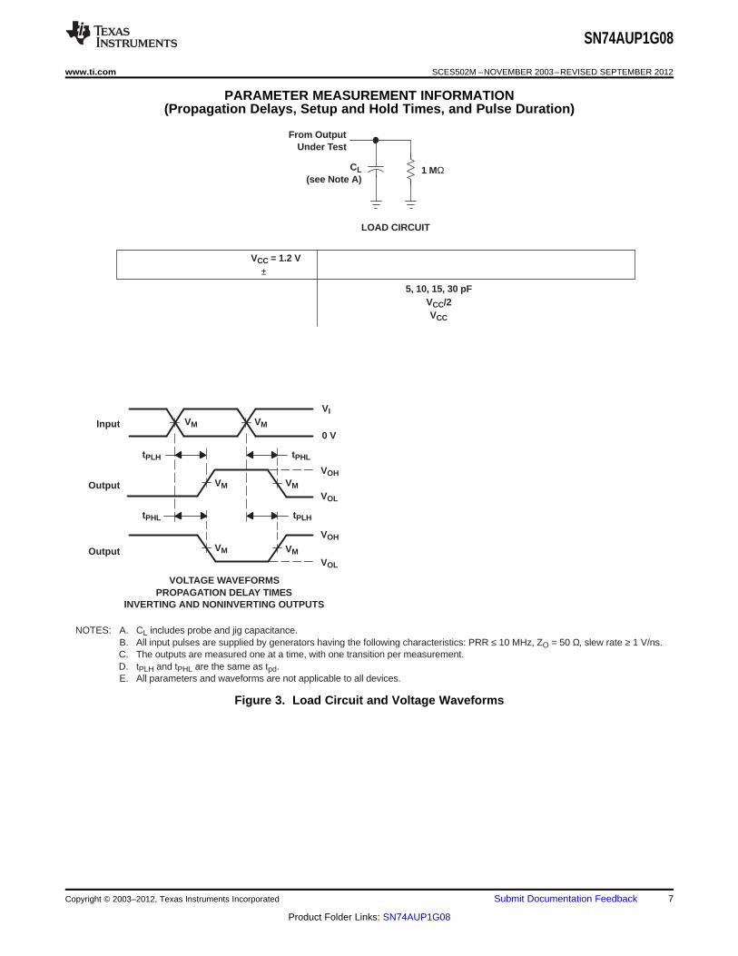
VM
From OutputUnder Test
CL(see Note A)
LOAD CIRCUIT
1 MΩ
VOLTAGE WAVEFORMSPROPAGATION DELAY TIMES
INVERTING AND NONINVERTING OUTPUTS
tPLH
tPHL
tPHL
tPLH
VOH
VOH
VOL
VOL
VI
0 VInput
Output
Output
NOTES: A. CL includes probe and jig capacitance.B. All input pulses are supplied by generators having the following characteristics: PRR ≤ 10 MHz, ZO = 50 Ω, slew rate ≥ 1 V/ns.C. The outputs are measured one at a time, with one transition per measurement.D. tPLH and tPHL are the same as tpd.E. All parameters and waveforms are not applicable to all devices.
VM VM
VM VM
VM
5, 10, 15, 30 pFVCC/2VCC
VCC = 1.2 V± 0.1 V
VCC = 0.8 VVCC = 1.5 V
± 0.1 VVCC = 1.8 V
± 0.15 VVCC = 2.5 V
± 0.2 VVCC = 3.3 V
± 0.3 V
5, 10, 15, 30 pFVCC/2VCC
5, 10, 15, 30 pFVCC/2VCC
5, 10, 15, 30 pFVCC/2VCC
CLVMVI
5, 10, 15, 30 pFVCC/2VCC
5, 10, 15, 30 pFVCC/2VCC
thtsu
Data Input
Timing InputVCC
0 V
VCC
0 V
0 V
tw
Input
VOLTAGE WAVEFORMSSETUP AND HOLD TIMES
VOLTAGE WAVEFORMSPULSE DURATION
VCC/2 VCC/2
VCC/2
VCC/2
VCC
VCC/2
SN74AUP1G08
www.ti.com SCES502M –NOVEMBER 2003–REVISED SEPTEMBER 2012
PARAMETER MEASUREMENT INFORMATION(Propagation Delays, Setup and Hold Times, and Pulse Duration)
Figure 3. Load Circuit and Voltage Waveforms
Copyright © 2003–2012, Texas Instruments Incorporated Submit Documentation Feedback 7
Product Folder Links: SN74AUP1G08

NOTES: A. CL includes probe and jig capacitance.B. Waveform 1 is for an output with internal conditions such that the output is low, except when disabled by the output control.
Waveform 2 is for an output with internal conditions such that the output is high, except when disabled by the output control.C. All input pulses are supplied by generators having the following characteristics: PRR ≤ 10 MHz, ZO = 50 Ω, slew rate ≥ 1 V/ns.D. The outputs are measured one at a time, with one transition per measurement.E. tPLZ and tPHZ are the same as tdis.F. tPZL and tPZH are the same as ten.G. All parameters and waveforms are not applicable to all devices.
5, 10, 15, 30 pFVCC/2VCC
0.15 V
VCC = 1.2 V± 0.1 V
VCC = 0.8 VVCC = 1.5 V
± 0.1 VVCC = 1.8 V
± 0.15 VVCC = 2.5 V
± 0.2 VVCC = 3.3 V
± 0.3 V
5, 10, 15, 30 pFVCC/2VCC0.1 V
5, 10, 15, 30 pFVCC/2VCC0.1 V
5, 10, 15, 30 pFVCC/2VCC0.1 V
CLVMVIV∆
5, 10, 15, 30 pFVCC/2VCC
0.15 V
5, 10, 15, 30 pFVCC/2VCC0.3 V
OutputWaveform 1
S1 at 2 × VCC(see Note B)
OutputWaveform 2
S1 at GND(see Note B)
VOL
VOH
tPZL
tPZH
tPLZ
tPHZ
VCC
0 V
VOL + V∆
VOH - V∆
≈0 V
VCC
VOLTAGE WAVEFORMSENABLE AND DISABLE TIMES
LOW- AND HIGH-LEVEL ENABLING
OutputControl
VCC/2 VCC/2
VCC/2
VCC/2
tPLZ/tPZLtPHZ/tPZH
2 × VCCGND
TEST S1From Output
Under Test
CL(see Note A)
LOAD CIRCUIT
S1
GND
5 kΩ
5 kΩ
2 × VCC
SN74AUP1G08
SCES502M –NOVEMBER 2003–REVISED SEPTEMBER 2012 www.ti.com
PARAMETER MEASUREMENT INFORMATION(Enable and Disable Times)
Figure 4. Load Circuit and Voltage Waveforms
8 Submit Documentation Feedback Copyright © 2003–2012, Texas Instruments Incorporated
Product Folder Links: SN74AUP1G08
SN74AUP1G08
www.ti.com SCES502M –NOVEMBER 2003–REVISED SEPTEMBER 2012
REVISION HISTORY
Changes from Revision J (May 2010) to Revision K Page
• Added new orderable package type SN74AUP1G08DSF2. ................................................................................................. 2
Changes from Revision K (October 2011) to Revision L Page
• Revised document to fix package addendum issue. ............................................................................................................ 1
Changes from Revision L (May 2012) to Revision M Page
• Added DPW package ordering information. ......................................................................................................................... 2
Copyright © 2003–2012, Texas Instruments Incorporated Submit Documentation Feedback 9
Product Folder Links: SN74AUP1G08
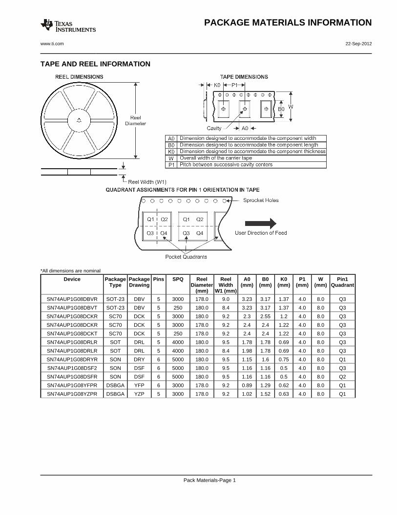
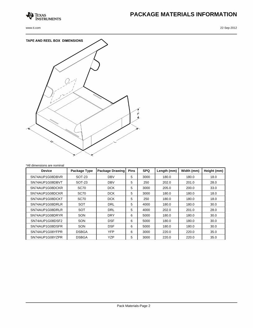
TAPE AND REEL INFORMATION
*All dimensions are nominal
Device PackageType
PackageDrawing
Pins SPQ ReelDiameter
(mm)
ReelWidth
W1 (mm)
A0(mm)
B0(mm)
K0(mm)
P1(mm)
W(mm)
Pin1Quadrant
SN74AUP1G08DBVR SOT-23 DBV 5 3000 178.0 9.0 3.23 3.17 1.37 4.0 8.0 Q3
SN74AUP1G08DBVT SOT-23 DBV 5 250 180.0 8.4 3.23 3.17 1.37 4.0 8.0 Q3
SN74AUP1G08DCKR SC70 DCK 5 3000 180.0 9.2 2.3 2.55 1.2 4.0 8.0 Q3
SN74AUP1G08DCKR SC70 DCK 5 3000 178.0 9.2 2.4 2.4 1.22 4.0 8.0 Q3
SN74AUP1G08DCKT SC70 DCK 5 250 178.0 9.2 2.4 2.4 1.22 4.0 8.0 Q3
SN74AUP1G08DRLR SOT DRL 5 4000 180.0 9.5 1.78 1.78 0.69 4.0 8.0 Q3
SN74AUP1G08DRLR SOT DRL 5 4000 180.0 8.4 1.98 1.78 0.69 4.0 8.0 Q3
SN74AUP1G08DRYR SON DRY 6 5000 180.0 9.5 1.15 1.6 0.75 4.0 8.0 Q1
SN74AUP1G08DSF2 SON DSF 6 5000 180.0 9.5 1.16 1.16 0.5 4.0 8.0 Q3
SN74AUP1G08DSFR SON DSF 6 5000 180.0 9.5 1.16 1.16 0.5 4.0 8.0 Q2
SN74AUP1G08YFPR DSBGA YFP 6 3000 178.0 9.2 0.89 1.29 0.62 4.0 8.0 Q1
SN74AUP1G08YZPR DSBGA YZP 5 3000 178.0 9.2 1.02 1.52 0.63 4.0 8.0 Q1
PACKAGE MATERIALS INFORMATION
www.ti.com 22-Sep-2012
Pack Materials-Page 1
*All dimensions are nominal
Device Package Type Package Drawing Pins SPQ Length (mm) Width (mm) Height (mm)
SN74AUP1G08DBVR SOT-23 DBV 5 3000 180.0 180.0 18.0
SN74AUP1G08DBVT SOT-23 DBV 5 250 202.0 201.0 28.0
SN74AUP1G08DCKR SC70 DCK 5 3000 205.0 200.0 33.0
SN74AUP1G08DCKR SC70 DCK 5 3000 180.0 180.0 18.0
SN74AUP1G08DCKT SC70 DCK 5 250 180.0 180.0 18.0
SN74AUP1G08DRLR SOT DRL 5 4000 180.0 180.0 30.0
SN74AUP1G08DRLR SOT DRL 5 4000 202.0 201.0 28.0
SN74AUP1G08DRYR SON DRY 6 5000 180.0 180.0 30.0
SN74AUP1G08DSF2 SON DSF 6 5000 180.0 180.0 30.0
SN74AUP1G08DSFR SON DSF 6 5000 180.0 180.0 30.0
SN74AUP1G08YFPR DSBGA YFP 6 3000 220.0 220.0 35.0
SN74AUP1G08YZPR DSBGA YZP 5 3000 220.0 220.0 35.0
PACKAGE MATERIALS INFORMATION
www.ti.com 22-Sep-2012
Pack Materials-Page 2
IMPORTANT NOTICE
Texas Instruments Incorporated and its subsidiaries (TI) reserve the right to make corrections, enhancements, improvements and otherchanges to its semiconductor products and services per JESD46, latest issue, and to discontinue any product or service per JESD48, latestissue. Buyers should obtain the latest relevant information before placing orders and should verify that such information is current andcomplete. All semiconductor products (also referred to herein as “components”) are sold subject to TI’s terms and conditions of salesupplied at the time of order acknowledgment.
TI warrants performance of its components to the specifications applicable at the time of sale, in accordance with the warranty in TI’s termsand conditions of sale of semiconductor products. Testing and other quality control techniques are used to the extent TI deems necessaryto support this warranty. Except where mandated by applicable law, testing of all parameters of each component is not necessarilyperformed.
TI assumes no liability for applications assistance or the design of Buyers’ products. Buyers are responsible for their products andapplications using TI components. To minimize the risks associated with Buyers’ products and applications, Buyers should provideadequate design and operating safeguards.
TI does not warrant or represent that any license, either express or implied, is granted under any patent right, copyright, mask work right, orother intellectual property right relating to any combination, machine, or process in which TI components or services are used. Informationpublished by TI regarding third-party products or services does not constitute a license to use such products or services or a warranty orendorsement thereof. Use of such information may require a license from a third party under the patents or other intellectual property of thethird party, or a license from TI under the patents or other intellectual property of TI.
Reproduction of significant portions of TI information in TI data books or data sheets is permissible only if reproduction is without alterationand is accompanied by all associated warranties, conditions, limitations, and notices. TI is not responsible or liable for such altereddocumentation. Information of third parties may be subject to additional restrictions.
Resale of TI components or services with statements different from or beyond the parameters stated by TI for that component or servicevoids all express and any implied warranties for the associated TI component or service and is an unfair and deceptive business practice.TI is not responsible or liable for any such statements.
Buyer acknowledges and agrees that it is solely responsible for compliance with all legal, regulatory and safety-related requirementsconcerning its products, and any use of TI components in its applications, notwithstanding any applications-related information or supportthat may be provided by TI. Buyer represents and agrees that it has all the necessary expertise to create and implement safeguards whichanticipate dangerous consequences of failures, monitor failures and their consequences, lessen the likelihood of failures that might causeharm and take appropriate remedial actions. Buyer will fully indemnify TI and its representatives against any damages arising out of the useof any TI components in safety-critical applications.
In some cases, TI components may be promoted specifically to facilitate safety-related applications. With such components, TI’s goal is tohelp enable customers to design and create their own end-product solutions that meet applicable functional safety standards andrequirements. Nonetheless, such components are subject to these terms.
No TI components are authorized for use in FDA Class III (or similar life-critical medical equipment) unless authorized officers of the partieshave executed a special agreement specifically governing such use.
Only those TI components which TI has specifically designated as military grade or “enhanced plastic” are designed and intended for use inmilitary/aerospace applications or environments. Buyer acknowledges and agrees that any military or aerospace use of TI componentswhich have not been so designated is solely at the Buyer's risk, and that Buyer is solely responsible for compliance with all legal andregulatory requirements in connection with such use.
TI has specifically designated certain components which meet ISO/TS16949 requirements, mainly for automotive use. Components whichhave not been so designated are neither designed nor intended for automotive use; and TI will not be responsible for any failure of suchcomponents to meet such requirements.
Products Applications
Audio www.ti.com/audio Automotive and Transportation www.ti.com/automotive
Amplifiers amplifier.ti.com Communications and Telecom www.ti.com/communications
Data Converters dataconverter.ti.com Computers and Peripherals www.ti.com/computers
DLP® Products www.dlp.com Consumer Electronics www.ti.com/consumer-apps
DSP dsp.ti.com Energy and Lighting www.ti.com/energy
Clocks and Timers www.ti.com/clocks Industrial www.ti.com/industrial
Interface interface.ti.com Medical www.ti.com/medical
Logic logic.ti.com Security www.ti.com/security
Power Mgmt power.ti.com Space, Avionics and Defense www.ti.com/space-avionics-defense
Microcontrollers microcontroller.ti.com Video and Imaging www.ti.com/video
RFID www.ti-rfid.com
OMAP Applications Processors www.ti.com/omap TI E2E Community e2e.ti.com
Wireless Connectivity www.ti.com/wirelessconnectivity
Mailing Address: Texas Instruments, Post Office Box 655303, Dallas, Texas 75265Copyright © 2012, Texas Instruments Incorporated