sn74auc1g08 single 2-input positive-and gate datasheet
TRANSCRIPT

1
24A
BY
Y� A • B or Y� A� B
Product
Folder
Order
Now
Technical
Documents
Tools &
Software
Support &Community
An IMPORTANT NOTICE at the end of this data sheet addresses availability, warranty, changes, use in safety-critical applications,intellectual property matters and other important disclaimers. PRODUCTION DATA.
SN74AUC1G08SCES374P –SEPTEMBER 2001–REVISED JUNE 2017
SN74AUC1G08 Single 2-Input Positive-AND Gate
1
1 Features1• Latch-Up Performance Exceeds 100 mA Per
JESD 78, Class II• ESD Protection Exceeds JESD 22
– 2000-V Human-Body Model (A114-A)– 200-V Machine Model (A115-A)– 1000-V Charged-Device Model (C101)
• Available in the Texas Instruments NanoFree™Package
• Optimized for 1.8-V Operation and Is 3.6-V I/OTolerant to Support Mixed-Mode Signal Operation
• Ioff Supports Partial-Power-Down Mode and BackDrive Protection
• Sub-1-V Operable• Max tpd of 2.4 ns at 1.8 V• Low Power Consumption, 10-µA Max ICC
• ±8-mA Output Drive at 1.8 V
2 Applications• AV Receiver• Audio Dock: Portable• Blu-Ray Player and Home Theater• Embedded PC• MP3 Player/Recorder (Portable Audio)• Personal Digital Assistant (PDA)• Power: Telecom/Server AC/DC Supply: Single
Controller: Analog and Digital• Solid State Drive (SSD): Client and Enterprise• TV: LCD/Digital and High-Definition (HDTV)• Tablet: Enterprise• Video Analytics: Server• Wireless Headset, Keyboard, and Mouse
3 DescriptionThis single 2-input positive-AND gate is operational at0.8-V to 2.7-V VCC, but is designed specifically for1.65-V to 1.95-V VCC operation.
The SN74AUC1G08 device performs the Booleanfunction in positive logic.
NanoFree™ package technology is a majorbreakthrough in IC packaging concepts, using the dieas the package.
This device is fully specified for partial-power-downapplications using Ioff. The Ioff circuitry disables theoutputs, preventing damaging current backflowthrough the device when it is powered down.
Device Information(1)
PART NUMBER PACKAGE BODY SIZE (NOM)SN74AUC1G08DBV SOT-23 (5) 2.90 mm × 1.60 mmSN74AUC1G08DCK SC70 (5) 2.00 mm × 1.25 mmSN74AUC1G08DRL SOT-5X3 (5) 1.60 mm × 1.20 mmSN74AUC1G08YZP DSBGA (5) 1.75 mm × 1.25 mm
(1) For all available packages, see the orderable addendum atthe end of the data sheet.
Logic Diagram (Positive Logic)
2
SN74AUC1G08SCES374P –SEPTEMBER 2001–REVISED JUNE 2017 www.ti.com
Product Folder Links: SN74AUC1G08
Submit Documentation Feedback Copyright © 2001–2017, Texas Instruments Incorporated
Table of Contents1 Features .................................................................. 12 Applications ........................................................... 13 Description ............................................................. 14 Revision History..................................................... 25 Pin Configuration and Functions ......................... 36 Specifications......................................................... 3
6.1 Absolute Maximum Ratings ...................................... 36.2 ESD Ratings.............................................................. 46.3 Recommended Operating Conditions....................... 46.4 Thermal Information .................................................. 46.5 Electrical Characteristics........................................... 56.6 Switching Characteristics: CL = 15 pF ...................... 56.7 Switching Characteristics: CL = 30 pF ...................... 5
6.8 Operating Characteristics.......................................... 57 Parameter Measurement Information .................. 68 Detailed Description .............................................. 7
8.1 Functional Block Diagram ......................................... 78.2 Device Functional Modes.......................................... 7
9 Device and Documentation Support.................... 89.1 Documentation Support ............................................ 89.2 Receiving Notification of Documentation Updates.... 89.3 Community Resources.............................................. 89.4 Trademarks ............................................................... 89.5 Electrostatic Discharge Caution................................ 89.6 Glossary .................................................................... 8
10 Mechanical, Packaging, and OrderableInformation ............................................................. 8
4 Revision HistoryNOTE: Page numbers for previous revisions may differ from page numbers in the current version.
Changes from Revision O (April 2007) to Revision P Page
• Deleted DRY Package throughout data sheet ....................................................................................................................... 1• Added Applications, Device Information table, ESD Ratings table, Thermal Information table, Detailed Description,
Device and Documentation Support, and Mechanical, Packaging, and Orderable Information ............................................ 1• Deleted Ordering Information, see Mechanical, Packaging, and Orderable Information ....................................................... 1

VCC
3
2
4
51A
Y
B
GND
1 2
C
B
A
Not to scale
GND Y
B
A VCC
3
2
4
51A VCC
Y
B
GND
2B
1A
3 4GND Y
5 VCC
3
SN74AUC1G08www.ti.com SCES374P –SEPTEMBER 2001–REVISED JUNE 2017
Product Folder Links: SN74AUC1G08
Submit Documentation FeedbackCopyright © 2001–2017, Texas Instruments Incorporated
5 Pin Configuration and Functions
DBV Package5-Pin SOT-23
Top View
DCK Package5-Pin SC70Top View
DRL Package5-Pin SOT-5X3
Top View
YZP Package5-Pin DSBGABottom View
Pin FunctionsPIN
I/O DESCRIPTIONNAME DBV, DCK,
DRL YZP
A 1 A1 I A logic inputB 2 B1 I B logic inputGND 3 C1 — GroundY 4 C2 O Y AND Logic OutputVCC 5 A2 — Positive Supply
(1) Stresses beyond those listed under Absolute Maximum Ratings may cause permanent damage to the device. These are stress ratingsonly, which do not imply functional operation of the device at these or any other conditions beyond those indicated under RecommendedOperating Conditions. Exposure to absolute-maximum-rated conditions for extended periods may affect device reliability.
(2) The input negative-voltage and output voltage ratings may be exceeded if the input and output current ratings are observed.
6 Specifications
6.1 Absolute Maximum Ratingsover operating free-air temperature range (unless otherwise noted) (1)
MIN MAX UNITVCC Supply voltage –0.5 3.6 VVI Input voltage (2) –0.5 3.6 VVO Voltage range applied to any output in the high-impedance or power-off state (2) –0.5 3.6 VVO Output voltage (2) –0.5 VCC + 0.5 VIIK Input clamp current VI < 0 –50 mAIOK Output clamp current VO < 0 –50 mAIO Continuous output current ±20 mA
Continuous current through VCC or GND ±100 mATstg Storage temperature –65 150 °C

4
SN74AUC1G08SCES374P –SEPTEMBER 2001–REVISED JUNE 2017 www.ti.com
Product Folder Links: SN74AUC1G08
Submit Documentation Feedback Copyright © 2001–2017, Texas Instruments Incorporated
(1) JEDEC document JEP155 states that 500-V HBM allows safe manufacturing with a standard ESD control process.(2) JEDEC document JEP157 states that 250-V CDM allows safe manufacturing with a standard ESD control process.
6.2 ESD RatingsVALUE UNIT
V(ESD) Electrostatic dischargeHuman-body model (HBM), per ANSI/ESDA/JEDEC JS-001 (1) 2000
VCharged-device model (CDM), per JEDEC specification JESD22-C101 (2) 1000Machine Model (A115-A) 200
(1) All unused inputs of the device must be held at VCC or GND to ensure proper device operation. See Implications of Slow or FloatingCMOS Inputs, SCBA004.
6.3 Recommended Operating ConditionsSee (1)
MIN MAX UNITVCC Supply voltage 0.8 2.7 V
VIH High-level input voltageVCC = 0.8 V to 1.95 V 0.65 × VCC VVCC = 2.3 V to 2.7 V 1.7
VIL Low-level input voltageVCC = 0.8 V to 1.95 V 0.35 × VCC VVCC = 2.3 V to 2.7 V 0.7
VI Input voltage 0 3.6 VVO Output voltage 0 VCC V
IOH High-level output current
VCC = 0.8 V –0.7
mAVCC = 1.1 V –3VCC = 1.4 V –5VCC = 1.65 V –8VCC = 2.3 V –9
IOL Low-level output current
VCC = 0.8 V 0.7
mAVCC = 1.1 V 3VCC = 1.4 V 5VCC = 1.65 V 8VCC = 2.3 V 9
Δt/Δv Input transition rise or fall rateVCC = 0.8 V to 1.95 V 20
ns/VVCC = 2.3 V to 2.7 V 10
TA Operating free-air temperature –40 85 °C
(1) For more information about traditional and new thermal metrics, see the Semiconductor and IC Package Thermal Metrics applicationreport.
6.4 Thermal Information
THERMAL METRIC (1)
SN74AUC1G08
UNITDBV (SOT-23) DCK (SC70) DRL (SOT-5X3)
YZP(DSBGA)
5 PINS 5 PINS 5 PINS 5 PINSRθJA Junction-to-ambient thermal resistance 206 252 142 132 °C/W
5
SN74AUC1G08www.ti.com SCES374P –SEPTEMBER 2001–REVISED JUNE 2017
Product Folder Links: SN74AUC1G08
Submit Documentation FeedbackCopyright © 2001–2017, Texas Instruments Incorporated
(1) All typical values are at TA = 25°C.
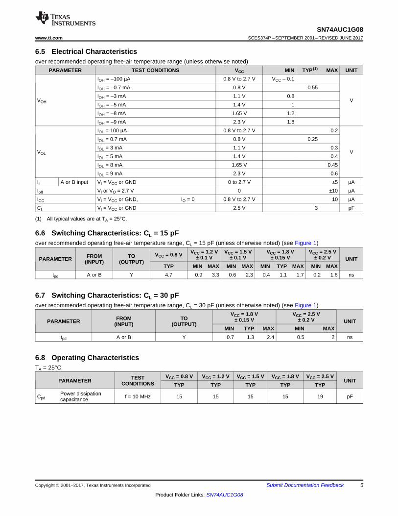
6.5 Electrical Characteristicsover recommended operating free-air temperature range (unless otherwise noted)
PARAMETER TEST CONDITIONS VCC MIN TYP (1) MAX UNIT
VOH
IOH = –100 µA 0.8 V to 2.7 V VCC – 0.1
V
IOH = –0.7 mA 0.8 V 0.55IOH = –3 mA 1.1 V 0.8IOH = –5 mA 1.4 V 1IOH = –8 mA 1.65 V 1.2IOH = –9 mA 2.3 V 1.8
VOL
IOL = 100 µA 0.8 V to 2.7 V 0.2
V
IOL = 0.7 mA 0.8 V 0.25IOL = 3 mA 1.1 V 0.3IOL = 5 mA 1.4 V 0.4IOL = 8 mA 1.65 V 0.45IOL = 9 mA 2.3 V 0.6
II A or B input VI = VCC or GND 0 to 2.7 V ±5 µAIoff VI or VO = 2.7 V 0 ±10 µAICC VI = VCC or GND, IO = 0 0.8 V to 2.7 V 10 µACI VI = VCC or GND 2.5 V 3 pF
6.6 Switching Characteristics: CL = 15 pFover recommended operating free-air temperature range, CL = 15 pF (unless otherwise noted) (see Figure 1)
PARAMETER FROM(INPUT)
TO(OUTPUT)
VCC = 0.8 V VCC = 1.2 V± 0.1 V
VCC = 1.5 V± 0.1 V
VCC = 1.8 V± 0.15 V
VCC = 2.5 V± 0.2 V UNIT
TYP MIN MAX MIN MAX MIN TYP MAX MIN MAXtpd A or B Y 4.7 0.9 3.3 0.6 2.3 0.4 1.1 1.7 0.2 1.6 ns
6.7 Switching Characteristics: CL = 30 pFover recommended operating free-air temperature range, CL = 30 pF (unless otherwise noted) (see Figure 1)
PARAMETER FROM(INPUT)
TO(OUTPUT)
VCC = 1.8 V± 0.15 V
VCC = 2.5 V± 0.2 V UNIT
MIN TYP MAX MIN MAXtpd A or B Y 0.7 1.3 2.4 0.5 2 ns
6.8 Operating CharacteristicsTA = 25°C
PARAMETER TESTCONDITIONS
VCC = 0.8 V VCC = 1.2 V VCC = 1.5 V VCC = 1.8 V VCC = 2.5 VUNIT
TYP TYP TYP TYP TYP
CpdPower dissipationcapacitance f = 10 MHz 15 15 15 15 19 pF

VCC/2
thtsu
From Output
Under Test
CL
(see Note A)
LOAD CIRCUIT
S1
2 × VCC
Open
GND
RL
RL
Data Input
Timing Input
VCC
0 V
VCC
0 V0 V
tw
Input
VOLTAGE WAVEFORMS
SETUP AND HOLD TIMES
VOLTAGE WAVEFORMS
PROPAGATION DELAY TIMES
INVERTING AND NONINVERTING OUTPUTS
VOLTAGE WAVEFORMS
PULSE DURATION
tPLH
tPHL
tPHL
tPLH
VOH
VOH
VOL
VOL
VCC
0 V
Input
Output
Waveform 1
S1 at 2 × VCC
(see Note B)
Output
Waveform 2
S1 at GND
(see Note B)
VOL
VOH
tPZL
tPZH
tPLZ
tPHZ
VCC
0 V
VOL + VD
VOH − VD
≈0 V
VCC
VOLTAGE WAVEFORMS
ENABLE AND DISABLE TIMES
LOW- AND HIGH-LEVEL ENABLING
Output
Output
tPLH/tPHL
tPLZ/tPZL
tPHZ/tPZH
Open
2 × VCC
GND
TEST S1
NOTES: A. CL includes probe and jig capacitance.
B. Waveform 1 is for an output with internal conditions such that the output is low, except when disabled by the output control.
Waveform 2 is for an output with internal conditions such that the output is high, except when disabled by the output control.
C. All input pulses are supplied by generators having the following characteristics: PRR≤ 10 MHz, ZO = 50 Ω, slew rate ≥ 1 V/ns.
D. The outputs are measured one at a time, with one transition per measurement.
E. tPLZ and tPHZ are the same as tdis.
F. tPZL and tPZH are the same as ten.
G. tPLH and tPHL are the same as tpd.
H. All parameters and waveforms are not applicable to all devices.
Output
Control
VCC/2 VCC/2
VCC/2 VCC/2
VCC/2 VCC/2
VCC/2
VCC/2 VCC/2
VCC/2
VCC/2
VCC/2
VCC
VCC/2
VCC/2
0.8 V
1.2 V ± 0.1 V
1.5 V ± 0.1 V
1.8 V ± 0.15 V
2.5 V ± 0.2 V
1.8 V ± 0.15 V
2.5 V ± 0.2 V
2 kΩ
2 kΩ
2 kΩ
2 kΩ
2 kΩ
1 kΩ
500 Ω
VCC RL
0.1 V
0.1 V
0.1 V
0.15 V
0.15 V
0.15 V
0.15 V
VDCL
15 pF
15 pF
15 pF
15 pF
15 pF
30 pF
30 pF
6
SN74AUC1G08SCES374P –SEPTEMBER 2001–REVISED JUNE 2017 www.ti.com
Product Folder Links: SN74AUC1G08
Submit Documentation Feedback Copyright © 2001–2017, Texas Instruments Incorporated
7 Parameter Measurement Information
Figure 1. Load Circuit and Voltage Waveforms
1
24A
BY
7
SN74AUC1G08www.ti.com SCES374P –SEPTEMBER 2001–REVISED JUNE 2017
Product Folder Links: SN74AUC1G08
Submit Documentation FeedbackCopyright © 2001–2017, Texas Instruments Incorporated
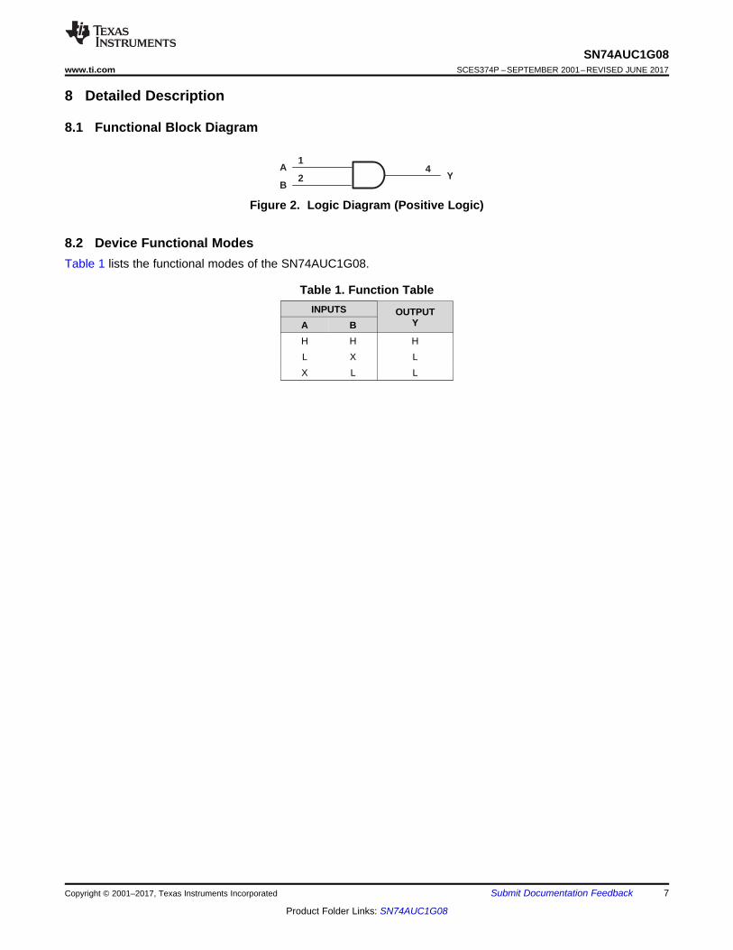
8 Detailed Description
8.1 Functional Block Diagram
Figure 2. Logic Diagram (Positive Logic)
8.2 Device Functional ModesTable 1 lists the functional modes of the SN74AUC1G08.
Table 1. Function TableINPUTS OUTPUT
YA BH H HL X LX L L

8
SN74AUC1G08SCES374P –SEPTEMBER 2001–REVISED JUNE 2017 www.ti.com
Product Folder Links: SN74AUC1G08
Submit Documentation Feedback Copyright © 2001–2017, Texas Instruments Incorporated
9 Device and Documentation Support
9.1 Documentation Support
9.1.1 Related DocumentationFor related documentation see the following:
Implications of Slow or Floating CMOS Inputs, SCBA004.
9.2 Receiving Notification of Documentation UpdatesTo receive notification of documentation updates, navigate to the device product folder on ti.com. In the upperright corner, click on Alert me to register and receive a weekly digest of any product information that haschanged. For change details, review the revision history included in any revised document.
9.3 Community ResourcesThe following links connect to TI community resources. Linked contents are provided "AS IS" by the respectivecontributors. They do not constitute TI specifications and do not necessarily reflect TI's views; see TI's Terms ofUse.
TI E2E™ Online Community TI's Engineer-to-Engineer (E2E) Community. Created to foster collaborationamong engineers. At e2e.ti.com, you can ask questions, share knowledge, explore ideas and helpsolve problems with fellow engineers.
Design Support TI's Design Support Quickly find helpful E2E forums along with design support tools andcontact information for technical support.
9.4 TrademarksNanoFree, E2E are trademarks of Texas Instruments.All other trademarks are the property of their respective owners.
9.5 Electrostatic Discharge CautionThese devices have limited built-in ESD protection. The leads should be shorted together or the device placed in conductive foamduring storage or handling to prevent electrostatic damage to the MOS gates.
9.6 GlossarySLYZ022 — TI Glossary.
This glossary lists and explains terms, acronyms, and definitions.
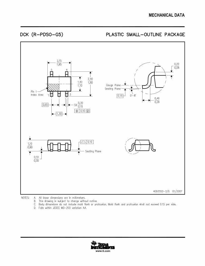
10 Mechanical, Packaging, and Orderable InformationThe following pages include mechanical, packaging, and orderable information. This information is the mostcurrent data available for the designated devices. This data is subject to change without notice and revision ofthis document. For browser-based versions of this data sheet, refer to the left-hand navigation.

PACKAGE OPTION ADDENDUM
www.ti.com 10-Dec-2020
Addendum-Page 1
PACKAGING INFORMATION
Orderable Device Status(1)
Package Type PackageDrawing
Pins PackageQty
Eco Plan(2)
Lead finish/Ball material
(6)
MSL Peak Temp(3)
Op Temp (°C) Device Marking(4/5)
Samples
SN74AUC1G08DBVR ACTIVE SOT-23 DBV 5 3000 RoHS & Green NIPDAU Level-1-260C-UNLIM -40 to 85 (U08K, U08R)
SN74AUC1G08DCKR ACTIVE SC70 DCK 5 3000 RoHS & Green NIPDAU Level-1-260C-UNLIM -40 to 85 (UE5, UEF, UEK, UE R)
SN74AUC1G08DCKRG4 ACTIVE SC70 DCK 5 3000 RoHS & Green NIPDAU Level-1-260C-UNLIM -40 to 85 (UE5, UEF, UEK, UE R)
SN74AUC1G08DRLR ACTIVE SOT-5X3 DRL 5 4000 RoHS & Green NIPDAU | NIPDAUAG Level-1-260C-UNLIM -40 to 85 (UE7, UER)
SN74AUC1G08DRLRG4 ACTIVE SOT-5X3 DRL 5 4000 RoHS & Green NIPDAUAG Level-1-260C-UNLIM -40 to 85 (UE7, UER)
SN74AUC1G08YZPR ACTIVE DSBGA YZP 5 3000 RoHS & Green SNAGCU Level-1-260C-UNLIM -40 to 85 UEN
(1) The marketing status values are defined as follows:ACTIVE: Product device recommended for new designs.LIFEBUY: TI has announced that the device will be discontinued, and a lifetime-buy period is in effect.NRND: Not recommended for new designs. Device is in production to support existing customers, but TI does not recommend using this part in a new design.PREVIEW: Device has been announced but is not in production. Samples may or may not be available.OBSOLETE: TI has discontinued the production of the device.
(2) RoHS: TI defines "RoHS" to mean semiconductor products that are compliant with the current EU RoHS requirements for all 10 RoHS substances, including the requirement that RoHS substancedo not exceed 0.1% by weight in homogeneous materials. Where designed to be soldered at high temperatures, "RoHS" products are suitable for use in specified lead-free processes. TI mayreference these types of products as "Pb-Free".RoHS Exempt: TI defines "RoHS Exempt" to mean products that contain lead but are compliant with EU RoHS pursuant to a specific EU RoHS exemption.Green: TI defines "Green" to mean the content of Chlorine (Cl) and Bromine (Br) based flame retardants meet JS709B low halogen requirements of <=1000ppm threshold. Antimony trioxide basedflame retardants must also meet the <=1000ppm threshold requirement.
(3) MSL, Peak Temp. - The Moisture Sensitivity Level rating according to the JEDEC industry standard classifications, and peak solder temperature.
(4) There may be additional marking, which relates to the logo, the lot trace code information, or the environmental category on the device.
(5) Multiple Device Markings will be inside parentheses. Only one Device Marking contained in parentheses and separated by a "~" will appear on a device. If a line is indented then it is a continuationof the previous line and the two combined represent the entire Device Marking for that device.
(6) Lead finish/Ball material - Orderable Devices may have multiple material finish options. Finish options are separated by a vertical ruled line. Lead finish/Ball material values may wrap to twolines if the finish value exceeds the maximum column width.

PACKAGE OPTION ADDENDUM
www.ti.com 10-Dec-2020
Addendum-Page 2
Important Information and Disclaimer:The information provided on this page represents TI's knowledge and belief as of the date that it is provided. TI bases its knowledge and belief on informationprovided by third parties, and makes no representation or warranty as to the accuracy of such information. Efforts are underway to better integrate information from third parties. TI has taken andcontinues to take reasonable steps to provide representative and accurate information but may not have conducted destructive testing or chemical analysis on incoming materials and chemicals.TI and TI suppliers consider certain information to be proprietary, and thus CAS numbers and other limited information may not be available for release.
In no event shall TI's liability arising out of such information exceed the total purchase price of the TI part(s) at issue in this document sold by TI to Customer on an annual basis.

TAPE AND REEL INFORMATION
*All dimensions are nominal
Device PackageType
PackageDrawing
Pins SPQ ReelDiameter
(mm)
ReelWidth
W1 (mm)
A0(mm)
B0(mm)
K0(mm)
P1(mm)
W(mm)
Pin1Quadrant
SN74AUC1G08DBVR SOT-23 DBV 5 3000 180.0 8.4 3.23 3.17 1.37 4.0 8.0 Q3
SN74AUC1G08DCKR SC70 DCK 5 3000 178.0 9.2 2.4 2.4 1.22 4.0 8.0 Q3
SN74AUC1G08DCKR SC70 DCK 5 3000 180.0 8.4 2.47 2.3 1.25 4.0 8.0 Q3
SN74AUC1G08DCKR SC70 DCK 5 3000 178.0 9.0 2.4 2.5 1.2 4.0 8.0 Q3
SN74AUC1G08DRLR SOT-5X3 DRL 5 4000 180.0 8.4 1.98 1.78 0.69 4.0 8.0 Q3
SN74AUC1G08DRLR SOT-5X3 DRL 5 4000 180.0 9.5 1.78 1.78 0.69 4.0 8.0 Q3
SN74AUC1G08YZPR DSBGA YZP 5 3000 178.0 9.2 1.02 1.52 0.63 4.0 8.0 Q1
PACKAGE MATERIALS INFORMATION
www.ti.com 13-Jan-2022
Pack Materials-Page 1

*All dimensions are nominal
Device Package Type Package Drawing Pins SPQ Length (mm) Width (mm) Height (mm)
SN74AUC1G08DBVR SOT-23 DBV 5 3000 202.0 201.0 28.0
SN74AUC1G08DCKR SC70 DCK 5 3000 180.0 180.0 18.0
SN74AUC1G08DCKR SC70 DCK 5 3000 202.0 201.0 28.0
SN74AUC1G08DCKR SC70 DCK 5 3000 180.0 180.0 18.0
SN74AUC1G08DRLR SOT-5X3 DRL 5 4000 202.0 201.0 28.0
SN74AUC1G08DRLR SOT-5X3 DRL 5 4000 184.0 184.0 19.0
SN74AUC1G08YZPR DSBGA YZP 5 3000 220.0 220.0 35.0
PACKAGE MATERIALS INFORMATION
www.ti.com 13-Jan-2022
Pack Materials-Page 2

www.ti.com
PACKAGE OUTLINE
C
0.220.08 TYP
0.25
3.02.6
2X 0.95
1.9
1.450.90
0.150.00 TYP
5X 0.50.3
0.60.3 TYP
80 TYP
1.9
A
3.052.75
B1.751.45
(1.1)
SOT-23 - 1.45 mm max heightDBV0005ASMALL OUTLINE TRANSISTOR
4214839/F 06/2021
NOTES: 1. All linear dimensions are in millimeters. Any dimensions in parenthesis are for reference only. Dimensioning and tolerancing per ASME Y14.5M.2. This drawing is subject to change without notice.3. Refernce JEDEC MO-178.4. Body dimensions do not include mold flash, protrusions, or gate burrs. Mold flash, protrusions, or gate burrs shall not exceed 0.25 mm per side.
0.2 C A B
1
34
5
2
INDEX AREAPIN 1
GAGE PLANE
SEATING PLANE
0.1 C
SCALE 4.000

www.ti.com
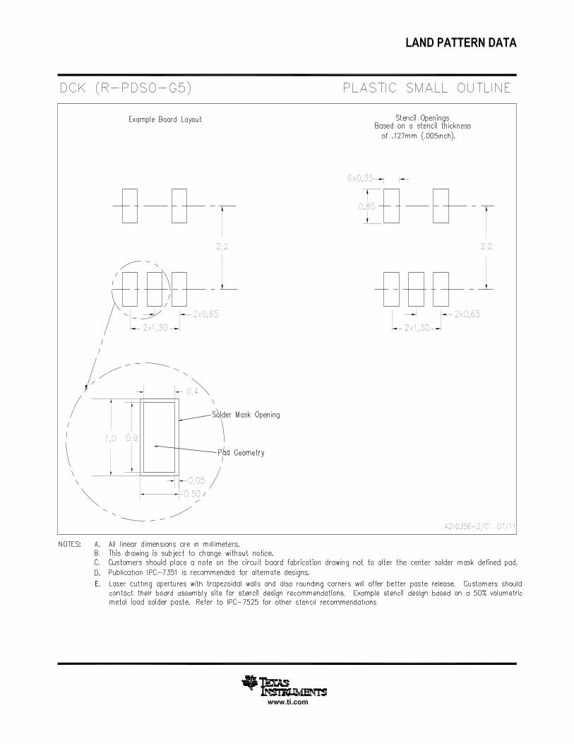
EXAMPLE BOARD LAYOUT
0.07 MAXARROUND
0.07 MINARROUND
5X (1.1)
5X (0.6)
(2.6)
(1.9)
2X (0.95)
(R0.05) TYP
4214839/F 06/2021
SOT-23 - 1.45 mm max heightDBV0005ASMALL OUTLINE TRANSISTOR
NOTES: (continued) 5. Publication IPC-7351 may have alternate designs. 6. Solder mask tolerances between and around signal pads can vary based on board fabrication site.
SYMM
LAND PATTERN EXAMPLEEXPOSED METAL SHOWN
SCALE:15X
PKG
1
3 4
5
2
SOLDER MASKOPENINGMETAL UNDER
SOLDER MASK
SOLDER MASKDEFINED
EXPOSED METAL
METALSOLDER MASKOPENING
NON SOLDER MASKDEFINED
(PREFERRED)
SOLDER MASK DETAILS
EXPOSED METAL

www.ti.com
EXAMPLE STENCIL DESIGN
(2.6)
(1.9)
2X(0.95)
5X (1.1)
5X (0.6)
(R0.05) TYP
SOT-23 - 1.45 mm max heightDBV0005ASMALL OUTLINE TRANSISTOR
4214839/F 06/2021
NOTES: (continued) 7. Laser cutting apertures with trapezoidal walls and rounded corners may offer better paste release. IPC-7525 may have alternate design recommendations. 8. Board assembly site may have different recommendations for stencil design.
SOLDER PASTE EXAMPLEBASED ON 0.125 mm THICK STENCIL
SCALE:15X
SYMM
PKG
1
3 4
5
2

www.ti.com
PACKAGE OUTLINE
C0.5 MAX
0.190.15
1TYP
0.5 TYP
5X 0.250.21
0.5TYP
B E A
D
4219492/A 05/2017
DSBGA - 0.5 mm max heightYZP0005DIE SIZE BALL GRID ARRAY
NOTES: 1. All linear dimensions are in millimeters. Any dimensions in parenthesis are for reference only. Dimensioning and tolerancing per ASME Y14.5M.2. This drawing is subject to change without notice.
BALL A1CORNER
SEATING PLANE
BALL TYP0.05 C
B
1 2
0.015 C A B
SYMM
SYMM
C
A
SCALE 8.000
D: Max =
E: Max =
1.418 mm, Min =
0.918 mm, Min =
1.358 mm
0.858 mm

www.ti.com
EXAMPLE BOARD LAYOUT
5X ( 0.23)(0.5) TYP
(0.5) TYP
( 0.23)METAL
0.05 MAX ( 0.23)SOLDER MASKOPENING
0.05 MIN
4219492/A 05/2017
DSBGA - 0.5 mm max heightYZP0005DIE SIZE BALL GRID ARRAY
NOTES: (continued) 3. Final dimensions may vary due to manufacturing tolerance considerations and also routing constraints. For more information, see Texas Instruments literature number SNVA009 (www.ti.com/lit/snva009).
SYMM
SYMM
LAND PATTERN EXAMPLESCALE:40X
1 2
A
B
C
NON-SOLDER MASKDEFINED
(PREFERRED)
SOLDER MASK DETAILSNOT TO SCALE
SOLDER MASKOPENING
SOLDER MASKDEFINED
METAL UNDERSOLDER MASK

www.ti.com
EXAMPLE STENCIL DESIGN
(0.5)TYP
(0.5) TYP
5X ( 0.25) (R0.05) TYP
METALTYP
4219492/A 05/2017
DSBGA - 0.5 mm max heightYZP0005DIE SIZE BALL GRID ARRAY
NOTES: (continued) 4. Laser cutting apertures with trapezoidal walls and rounded corners may offer better paste release.
SYMM
SYMM
SOLDER PASTE EXAMPLEBASED ON 0.1 mm THICK STENCIL
SCALE:40X
1 2
A
B
C

www.ti.com
PACKAGE OUTLINE
C
1.71.5
2X 0.5
2X 1
5X 0.30.1
0.6 MAX
5X 0.180.08
5X 0.40.2
0.050.00 TYP
5X 0.270.15
B 1.31.1
A
1.71.5
NOTE 3
SOT - 0.6 mm max heightDRL0005APLASTIC SMALL OUTLINE
4220753/B 12/2020
NOTES: 1. All linear dimensions are in millimeters. Any dimensions in parenthesis are for reference only. Dimensioning and tolerancing per ASME Y14.5M.2. This drawing is subject to change without notice.3. This dimension does not include mold flash, protrusions, or gate burrs. Mold flash, protrusions, or gate burrs shall not exceed 0.15 mm per side.4. Reference JEDEC registration MO-293 Variation UAAD-1
1 5
PIN 1ID AREA
34
SEATING PLANE
0.05 C
SCALE 8.000
0.1 C A B0.05
SYMM
SYMM

www.ti.com
EXAMPLE BOARD LAYOUT
0.05 MAXAROUND
0.05 MINAROUND
5X (0.67)
5X (0.3)
(1.48)
2X (0.5)
(R0.05) TYP
(1)
4220753/B 12/2020
SOT - 0.6 mm max heightDRL0005APLASTIC SMALL OUTLINE
NOTES: (continued) 5. Publication IPC-7351 may have alternate designs. 6. Solder mask tolerances between and around signal pads can vary based on board fabrication site.
SYMM
LAND PATTERN EXAMPLESCALE:30X
SYMM1
3 4
5
SOLDER MASKOPENING
METAL UNDERSOLDER MASK
SOLDER MASKDEFINED
METALSOLDER MASKOPENING
NON SOLDER MASKDEFINED
(PREFERRED)
SOLDERMASK DETAILS

www.ti.com
EXAMPLE STENCIL DESIGN
(1.48)
2X (0.5)
5X (0.67)
5X (0.3)
(R0.05) TYP
(1)
SOT - 0.6 mm max heightDRL0005APLASTIC SMALL OUTLINE
4220753/B 12/2020
NOTES: (continued) 7. Laser cutting apertures with trapezoidal walls and rounded corners may offer better paste release. IPC-7525 may have alternate design recommendations. 8. Board assembly site may have different recommendations for stencil design.
SOLDER PASTE EXAMPLEBASED ON 0.1 mm THICK STENCIL
SCALE:30X
SYMM
SYMM1
3 4
5

IMPORTANT NOTICE AND DISCLAIMERTI PROVIDES TECHNICAL AND RELIABILITY DATA (INCLUDING DATA SHEETS), DESIGN RESOURCES (INCLUDING REFERENCE DESIGNS), APPLICATION OR OTHER DESIGN ADVICE, WEB TOOLS, SAFETY INFORMATION, AND OTHER RESOURCES “AS IS” AND WITH ALL FAULTS, AND DISCLAIMS ALL WARRANTIES, EXPRESS AND IMPLIED, INCLUDING WITHOUT LIMITATION ANY IMPLIED WARRANTIES OF MERCHANTABILITY, FITNESS FOR A PARTICULAR PURPOSE OR NON-INFRINGEMENT OF THIRD PARTY INTELLECTUAL PROPERTY RIGHTS.These resources are intended for skilled developers designing with TI products. You are solely responsible for (1) selecting the appropriate TI products for your application, (2) designing, validating and testing your application, and (3) ensuring your application meets applicable standards, and any other safety, security, regulatory or other requirements.These resources are subject to change without notice. TI grants you permission to use these resources only for development of an application that uses the TI products described in the resource. Other reproduction and display of these resources is prohibited. No license is granted to any other TI intellectual property right or to any third party intellectual property right. TI disclaims responsibility for, and you will fully indemnify TI and its representatives against, any claims, damages, costs, losses, and liabilities arising out of your use of these resources.TI’s products are provided subject to TI’s Terms of Sale or other applicable terms available either on ti.com or provided in conjunction with such TI products. TI’s provision of these resources does not expand or otherwise alter TI’s applicable warranties or warranty disclaimers for TI products.TI objects to and rejects any additional or different terms you may have proposed. IMPORTANT NOTICE
Mailing Address: Texas Instruments, Post Office Box 655303, Dallas, Texas 75265Copyright © 2022, Texas Instruments Incorporated