sn65dsi83, sn65dsi84, and sn65dsi85 evm user s manual and
TRANSCRIPT

1SLLU221–October 2016Submit Documentation Feedback
Copyright © 2016, Texas Instruments Incorporated
SN65DSI83, SN65DSI84, and SN65DSI85 EVM User’s Manual andImplementation Guide
User's GuideSLLU221–October 2016
SN65DSI83, SN65DSI84, and SN65DSI85 EVM User’sManual and Implementation Guide
This document describes how to use and configure the SN65DSI83, SN65DSI84, or SN65DSI85 EVM.Hereafter in this document, the SN65DSI83, SN65DSI84, and SN65DSI85 devices may be referred to asSN65DSI8X.
Contents1 Overview ...................................................................................................................... 2
1.1 What are the SN65DSI83, SN65DSI84, and SN65DSI85? ................................................... 21.2 What is the SN65DSI8X EVM? ................................................................................... 21.3 What is Included in the SN65DSI8X EVM? ..................................................................... 31.4 What Does This EVM Look Like? ................................................................................ 3
2 Hardware Description ....................................................................................................... 42.1 Connectors for DSI8X Input Ports ................................................................................ 42.2 Connectors for DSI85 Output Ports .............................................................................. 42.3 I2C .................................................................................................................... 52.4 Enable or Reset ..................................................................................................... 52.5 Power................................................................................................................. 52.6 Backlight Driver ..................................................................................................... 52.7 Reference CLK Programmability ................................................................................. 62.8 DIP Switch Configuration .......................................................................................... 6
3 Quick Start Guide ............................................................................................................ 64 References ................................................................................................................... 75 EVM Schematics............................................................................................................. 8
List of Figures
1 SN65DSI8XEVM ............................................................................................................. 32 SN65DSI8X EVM Block Diagram.......................................................................................... 43 DSI EVM Example Setup ................................................................................................... 74 SN65DSI8X Schematic 1 ................................................................................................... 85 SN65DSI8X Schematic 2 ................................................................................................... 96 SN65DSI8X Schematic 3 ................................................................................................. 107 SN65DSI8X Schematic 4.................................................................................................. 11
List of Tables
1 SN65DSI8X Features Summary........................................................................................... 22 DIP Switch Setting ........................................................................................................... 6

Overview www.ti.com
2 SLLU221–October 2016Submit Documentation Feedback
Copyright © 2016, Texas Instruments Incorporated
SN65DSI83, SN65DSI84, and SN65DSI85 EVM User’s Manual andImplementation Guide
1 Overview
1.1 What are the SN65DSI83, SN65DSI84, and SN65DSI85?The SN65DSI8X is a MIPI DSI-to-LVDS bridge device that supports video modes in the forward direction.The SN65DSI8X is primarily targeted for portable applications such as tablets and smart phones thatutilize the MIPI DSI video format. Use the SN65DSI8X between a GPU with DSI output and a video panelwith LVDS inputs.
All three devices share the same pin out and package.
Table 1 is a summary of the feature sets on these devices:
Table 1. SN65DSI8X Features Summary
Part Name Description Max ResolutionSN65DSI83 Single-channel DSI to single-link LVDS Suitable 1366×768/1280×60 fps at 24 bpp/18 bppSN65DSI84 Single-channel DSI to two single-link LVDS 1920×1200 60 fps at 24 bpp/18 bppSN65DSI85 Dual-channel DSI to two single-link LVDS 2560×1600 60 fps, 1920×1080p 120 fps at 24 bpp /18 bpp
NOTE: Each DSI channel has 4 DSI data lanes + 1 CLK lane. Each LVDS link has 4 data lanes + 1CLK lane.
1.2 What is the SN65DSI8X EVM?The SN65DSI8X EVM is a PCB created to help customers implementing SN65DSI83, SN65DSI84, andSN65DSI85 in system hardware. This EVM can be used as a hardware reference design for anyimplementation using the SN65DSI8X. The SN65DSI8X EVM is designed for use across all three versionsof the DSI bridge devices - SN65DSI83, SN65DSI84, and SN65DSI85. PCB design and layout files areprovided upon request to aid PCB design with a SN65DSI8X component. The layout files are used as aguideline to implement the SN65DSI8X with illustrations of the routing and placement rules. Please notethat the EVM design includes test components to evaluate the SN65DSI8X which may not applicable forproduction.
This EVM includes on-board connectors for DSI input and LVDS output signals. These connectorsconnect MIPI DPHY-compliant DSI source and LVDS panels to the EVM. Refer to Section 2.1 andSection 2.2 for more information on the connectors.
CAUTIONA custom translator cable or card is required if this EVM is to be utilized for theevaluation of an implementation from the customer. Any other method ofconnecting to any DSI source or LVDS panel is not supported by this EVM. TIis not responsible for any issues or problems that may occur as a result ofusing connection methods other than what is recommended in this document.
NOTE: Some portions and components in the EVM or in this document may include the referencesto SN65DSI85 instead of addressing all three part numbers. The SN65DSI85 is replaceablewith SN65DSI83 or SN65DSI84.
www.ti.com Overview
3SLLU221–October 2016Submit Documentation Feedback
Copyright © 2016, Texas Instruments Incorporated
SN65DSI83, SN65DSI84, and SN65DSI85 EVM User’s Manual andImplementation Guide
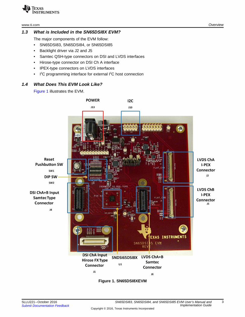
1.3 What is Included in the SN65DSI8X EVM?The major components of the EVM follow:• SN65DSI83, SN65DSI84, or SN65DSI85• Backlight driver via J2 and J5• Samtec QSH-type connectors on DSI and LVDS interfaces• Hirose-type connector on DSI Ch A interface• IPEX-type connectors on LVDS interfaces• I2C programming interface for external I2C host connection
1.4 What Does This EVM Look Like?Figure 1 illustrates the EVM.
Figure 1. SN65DSI8XEVM

5V
3.3V
1.8V
9V
DSI85
DSI85 Input LVDS Output
I2C Logic Reset Logic
Backlight Driver
CDC -Optional RefCLKgeneration
HiroseFX Conn
SMA/Samtec
OR
DSI_CHA_CLK
DSI_CHB_CLK
DSI_CHA_DATAP/N[3:0]
DSI_CHB_DATAP/N[3:0]
LVDS_CHA_CLK
LVDS_CHB_CLK
LVDS_CHA_DATAP/N[3:0]
LVDS_CHB_DATAP/N[3:0]
I-PEX20455
SMA/Samtec
OR
Ref_CLK IN
Page 2
Page 3Page 3
Page 3,5
Page 5
Page 4 Page 4
Page 4
Copyright © 2016, Texas Instruments Incorporated
Hardware Description www.ti.com
4 SLLU221–October 2016Submit Documentation Feedback
Copyright © 2016, Texas Instruments Incorporated
SN65DSI83, SN65DSI84, and SN65DSI85 EVM User’s Manual andImplementation Guide
2 Hardware DescriptionFigure 2 shows the EVM block diagram.
Figure 2. SN65DSI8X EVM Block Diagram
2.1 Connectors for DSI8X Input PortsThe EVM has two input options for DSI video. If a custom breakout board is to be designed using theseoptions, a schematic and an allegro PCB symbol for either connector is provided by TI upon request.(A) J4 - Samtec QSH-type connector (P/N QSH-020-01-H-D-DP-A)
J4 is a Samtec QSH-type connector that can be mated with a matching QTH-type connector on thetop. It provides DSI input connections to both DSI Ch A and Ch B signals. It also provides access toI2C and other miscellaneous signals such as IRQ. XC connections are open vias just in case there is aneed for connection to other signals. The mating connector part number is QTH-020-01-H-D-DP-A. Foran SMA-type connection, use the Samtec HDR-128291-XX breakout board. The HDR-128291-XX is abreakout board with a mating connector to J4 and standard SMA male connectors via cables. Moreinformation on this breakout board is provided upon request.
(B) J1 – Hirose FX-type connector (P/N FX6A-40S-0.8SV2)J1 is a Hirose FX-type connector that can be mated with a matching FX plug on the top. The partnumber for the mating connector is FX6A-40P-0.8SV2. J1 provides DSI input connection only to theDSI Ch A signals. It also provides access to I2C and other miscellaneous signals such as IRQ.
2.2 Connectors for DSI85 Output PortsThere are two output port options available on the EVM for the LVDS output signals. If a custom breakoutboard is to be designed using these options, a schematic and an allegro PCB symbol for either connectorcan be provided by TI.(A) J6 - Samtec QSH-type connector (P/N QSH-020-01-H-D-DP-A)
J6 is a Samtec QSH-type connector that can be mated with a matching QTH-type connector on thetop. It provides DSI input connections to both LVDS Ch A and Ch B signals. It also provides access to

www.ti.com Hardware Description
5SLLU221–October 2016Submit Documentation Feedback
Copyright © 2016, Texas Instruments Incorporated
SN65DSI83, SN65DSI84, and SN65DSI85 EVM User’s Manual andImplementation Guide
the backlight power and its related signals. XC connections are open vias, in case there is a need toconnect to other signals. The mating connector part number is QTH-020-01-H-D-DP-A. For an SMA-type connection, use the Samtec HDR-128291-XX breakout board. The HDR-128291-XX is a breakoutboard with a mating connector to J6 and standard SMA male connectors via cables. More informationon this breakout board is provided upon request.
(B) J2 and J5 – I-PEX-type connectors (P/N 20455-040E-12)J2 and J5 are I-PEX connectors widely used in LCD video panels with LVDS receivers. Connect J2and J5 via an SGC-type cable with one-to-one pin mapping to a panel using the I-PEX20455-040E-12connectors. J2 connects to the LVDS Ch A signals while J5 connects to the LVDS CHB signals.
2.3 I2CAccess to I2C signals are provided via DSI input connectors J1 and J4 (as mentioned in Section 2.1) orJ10. Note that I2C signal levels should be at 1.8 V when the I2C interface is accessed through connectorsJ1 or J4. A 3.3-V to 1.8-V voltage translation is provided when an I2C host is connected through J10.
A stand-alone external I2C host can be connected via J10 to debug.
2.4 Enable or ResetThere are three device enable or reset options to use with the EVM:(A) Supervisor circuitry option
This is a default configuration. The enable (EN) signal is held low until the power good (PG) from the1.8-V voltage regulator reaches a stable high voltage level, then it is released high.
(B) RC timing optionThe C10 external capacitor and internal resistor are used to control the EN ramp time after the deviceis powered on. C10 is a DNI (Do Not Install option), by default. C10 needs to be installed and R52needs to be uninstalled to enable this option.
(C) External control optionA push button (SW1) or a DIP switch (SW2.3) is available for the manual control of the EN signal.Install R64 to enable the DIP switch option.
2.5 PowerA 5- to 6-V power supply will operate the SN65DSI8X EVM. A plug to accept a 5- to 6-V wall poweradapter is provided on the EVM (J13). The jumper on position 1-2 of J15 should be placed while J14 isleft open. This should be the default configuration when the board is shipped.The EVM is designed to accommodate up to maximum of 1.5 A current. The current consumption ofthe board without backlight driver enabled is about 70 mA + SN65DSI85 device power. TheSN65DSI85 consumes about 50 mA at power on, approximately 80 mA to approximately 200 mA,depending on the system configuration. The total power consumption of the board could varydepending on LCD panels when the on-board backlight driver is used. When an LCD panel consumesmore current than 1.5 A minus 70 mA + SN65DSI85 device power, an external backlight source shouldbe used.
NOTE: Do not plug in any power source higher than the configured voltage (5 V or 6 V).
2.6 Backlight DriverThe SN65DSI8X EVM incorporates the LED backlight driver circuitry using the TI backlight driver deviceTPS61181A enabling use of the on-board backlight driver source. The default configuration of the EVMenables the on-board backlight driver.
If the external backlight driver is used, a connection is available via J3. Uninstall FB6 if external backlightdriver is used.

Hardware Description www.ti.com
6 SLLU221–October 2016Submit Documentation Feedback
Copyright © 2016, Texas Instruments Incorporated
SN65DSI83, SN65DSI84, and SN65DSI85 EVM User’s Manual andImplementation Guide
2.7 Reference CLK ProgrammabilityThe SN65DSI8X EVM incorporates a programmable CLK circuitry using a TI-programmable device,CDCEL913. The output of the CDCEL913 is connected to the reference CLK of the SN65DSI8X. Thedefault frequency of the reference CLK is 27 MHz. The CLK can be programmed via I2C signals broughtout to on-board connectors J9, J12, or J10. When J10 is used, place jumpers on J9 and J12. Thereference CLK can be pre-programmed to a desired value, if requested prior to shipping.
2.8 DIP Switch ConfigurationA DIP switch is provided to operate the device or EVM in different configurations. When the switch is in anopen position, the corresponding signal is tied high. When the switch is in the ON (closed) position, thecorresponding signal is tied to GND.
The signals in the greyed out region are not enabled unless a corresponding resistor is installed.
Table 2. DIP Switch Setting
DIP SW No Signal Name DescriptionDefault Configuration
Open(Off)HIGH
Closed(On)LOW
SW2-1 DIP1 – Dimming CTRL orLED_BKLT_EN
Controls LED backlight driver enable in defaultconfiguration.Installing R100 and uninstalling R63 enablescontrol on dimming control of the backlightdriver.Always switch back to closed (ON) positionprior to unplug or plug operation of the panel.
x
SW2-2 I2C_3V3EN Enables 3.3-V voltage translator for the I2Csignals x
SW2-3 BRD_RSTN Controls the EN/RESET signal of theSN65DSI8X high or low x
SW2-4 RSVD1 Reserved xSW2-5 RSVD2 Reserved x
SW2-6 ADDR Controls the ADDR signal of the SN65DSI8Xhigh or low x
SW2-7 PWMIN Controls the PWMIN of J6 high or low x
SW2-8 LED_EN
Controls the LED_EN of J2 or J5 high or lowThis switch should be toggled high to enablethe LED of the connected panel.Always switch back to closed (ON) positionprior to unplug or plug operation of the panel.
x
3 Quick Start GuideQuick-start instructions are provided in the following list:1. Plug in a DSI source to J42. Plug in a LVDS video sink device on J2, J5 or J63. Plug in an I2C host on J10 if an external I2C host is used.4. Make sure the DIP switch setting is in a correct configuration.5. Apply power to the EVM. The following LEDs should light up: D3, D6, and D7. D1 may light up
depending on the configuration.6. Start video streaming on the DSI input7. Configure the device for the desired mode of operation via I2C. Video output should be observed after
configuration is complete.

www.ti.com References
7SLLU221–October 2016Submit Documentation Feedback
Copyright © 2016, Texas Instruments Incorporated
SN65DSI83, SN65DSI84, and SN65DSI85 EVM User’s Manual andImplementation Guide
Figure 3 depicts the setup using an external I2C host, Samtec-to-SMA breakout board (HDR-128291-XX)for DSI ChA input and a 1024×600 video panel over an I-PEX connector.
Figure 3. DSI EVM Example Setup
4 References1. SN65DSI8X Datasheets (SN65DSI83 SLLSEC1), (SN65DSI84 SLLSEC2), (SN65DSI85 SLLSEB9)

LEAVEUNCONNECTEDFOR NORMALOPERATION
ADDR = 1, Slave Addr = 0x2DADDR = 0, Slave Addr = 0x2C
Reset(EN) can be implemented with passivecomponents as shown or active circuitry. Incase of using passive components, thevalues of the RC circuitry need to beadjusted to make sure the low to hightransition occurs after the Vcc supply hasreached the minimum recommendedoperating voltage. For this reason, it isrecommended to USE ACTIVE CIRCUITRY forbetter control of the RESET/EN timing.
DSI INPUT LVDS OUTPUT
Optional ref CLKfor LVDS PixelCLK
25MHz-154MHz
1uF is min value.
The number of capacitors and their values may vary depending on the system implementation
R5: Terminate to GNDwith a pull-downresistor if unused
0.2uF
SN65DSI85
Reset Implementation
Note: Bypass caps and FBshould be placed near U1SN65DSI85.
*IMPORTANT*If REFCLK is to beused, the CLK tracelength between theREFCLK terminal andthe source of the REFCLK(OSC or Xtal)should be kept as shortas possble.
IRQSilkScreen:
SilkScreen: IRQ
SilkScreen: REF_CLK
DSI_A0PDSI_A0N
DSI_A1NDSI_A2PDSI_A2NDSI_A3PDSI_A3NDSI_ACLKPDSI_ACLKN
DSI_A1P
FlatChA_Y0NFlatChA_Y0P
FlatChA_Y1PFlatChA_Y2NFlatChA_Y2PFlatChA_Y3NFlatChA_Y3PFlatChA_YCLKNFlatChA_YCLKP
FlatChA_Y1N
ADDR
Test1Test2
BOARD_RESETN
IRQ
DSI_B0PDSI_B0N
DSI_B1NDSI_B2PDSI_B2NDSI_B3PDSI_B3NDSI_BCLKPDSI_BCLKN
DSI_B1PFlatChB_Y0PFlatChB_Y0N
FlatChB_Y1PFlatChB_Y2NFlatChB_Y2PFlatChB_Y3NFlatChB_Y3PFlatChB_YCLKNFlatChB_YCLKP
FlatChB_Y1N
I2C_SCLI2C_SDA
BOARD_RESETN
Vcore_1P1_Out
IRQ_LEDIRQ IRQ_OUT
REFCLK
EXT_REFCLK
Vcc_1P8V
BOARD_1P8V
BOARD_1P8V BOARD_1P8V
Vcc_1P8V
BOARD_1P8V BOARD_3P3V
DSI_A0Ppg3DSI_A0Npg3DSI_A1Ppg3DSI_A1Npg3DSI_A2Ppg3DSI_A2Npg3DSI_A3Ppg3DSI_A3Npg3DSI_ACLKPpg3DSI_ACLKNpg3
DSI_B0Ppg3DSI_B0Npg3DSI_B1Ppg3DSI_B1Npg3DSI_B2Ppg3DSI_B2Npg3DSI_B3Ppg3DSI_B3Npg3DSI_BCLKPpg3DSI_BCLKNpg3
I2C_SCL pg3,4I2C_SDA pg3,4
LVDS_RefCLK pg4
FlatChA_Y0N pg3FlatChA_Y0P pg3FlatChA_Y1N pg3FlatChA_Y1P pg3FlatChA_Y2N pg3FlatChA_Y2P pg3FlatChA_Y3N pg3FlatChA_Y3P pg3FlatChA_CLKN pg3FlatChA_CLKP pg3
FlatChB_Y0N pg3FlatChB_Y0P pg3FlatChB_Y1N pg3FlatChB_Y1P pg3FlatChB_Y2N pg3FlatChB_Y2P pg3FlatChB_Y3N pg3FlatChB_Y3P pg3FlatChB_CLKN pg3FlatChB_CLKP pg3
BOARD_RESETNpg2,3,4
BOARD_RESETNpg2,3,4
ADDRpg4
IRQ pg3Test1pg4Test2pg4
R4
4.7K
R32
DNI
J17HDR2X1 M .1
12
C111uF
C110uF
R1
0
C5
10000pF
TP1
T POINT S
C2
1.0uF
R5
10K
C3
10000pF
D1
LED Orange 0805
C7
10000pF
U1
SN65DSI85
DA0PH3
DA1PH4
DA2PH6
DA3PH7
DACPH5
DB0PC2
DB1PD2
DB2PF2
DB3PG2
DBCPE2
DA0NJ3
DA1NJ4
DA2NJ6
DA3NJ7
DACNJ5
DB0NC1
DB1ND1
DB2NF1
DB3NG1
DBCNE1
A_Y0NC9
A_Y1ND9
A_Y2NE9
A_Y3NG9
A_CLKNF9
A_Y0PC8
A_Y1PD8
A_Y2PE8
A_Y3PG8
A_CLKPF8
B_Y0NA3
B_Y0PB3
B_Y1NA4
B_Y1PB4
B_Y2NA5
B_Y2PB5
B_Y3NA7
B_Y3PB7
B_CLKNA6
B_CLKPB6
ADDRA1
SDAJ1SCLH1
ENB1
TEST2B2 TEST1H8
REFCLKH2
IRQJ9
Vcc
A9
Vcc
B8
Vcc
D6
Vcc
E6
Vcc
F6
Vcc
J2
Vcc
E5
GN
DB
9
GN
DA
8
GN
DA
2
GN
DD
5
GN
DE
4
GN
DF
4
GN
DF
5
GN
DH
9
Vcore
J8
C6
0.1uF
R2
348
LP3
LP2LP1
FB1
220 @ 100MHZC4
0.1uF
C9
0.1uF
C8
0.1uF
R33 0
R3
4.7K
C10
DNI
U2SN74LVC1G07DCK
2
35
4
1
Copyright © 2016, Texas Instruments Incorporated
EVM Schematics www.ti.com
8 SLLU221–October 2016Submit Documentation Feedback
Copyright © 2016, Texas Instruments Incorporated
SN65DSI83, SN65DSI84, and SN65DSI85 EVM User’s Manual andImplementation Guide
5 EVM SchematicsFigure 4 through Figure 7 illustrate the EVM schematics.
Figure 4. SN65DSI8X Schematic 1

NOTE:This connector is to interface DSIA Chusing FX64-40P-0.8SV Type plug.
DSI ChA DisplayExpansion Connector
BOTTOM VIEW
NOTE:- Remove R6-R15 for DSI source connected to J4- Populate R6-R15 when a source connected through J1**R6 - R15 to be placed as near as J4 to avoid stub when J1 is not in use**
WARNING20455-040E-12 has nopin1 datum mark.20455-040E-0X seriesis same connectorwith pin1 datum mark,however the datummark is on theopposite end of wherepin 1 is.
Note: This header is for supplying backlightpowerto flat panels with LED backlight. The pinoutmathces the connector definition of the backlight driver TPS61181 EVM.
Samtec to SMA Connector for DSIA and DSIB
NOTE:This connector is to interface DSI interfacewith any source with SMA connectors viaSamtec to SMA cable
Samtec to SMA Connector for Flatlink
NOTE:This connector is to interfaceFlatlink LVDS interfaceto LCDPanels via breakout boards withFlatlink LCD panel connector
Note: Bypasscaps.
Note: Bypasscaps.
Note: Bypasscaps
Note: Bypasscaps.
I-PEX 20455 Flatpanel Connectors
Flat ChASilkScreen:
Flat ChBSilkScreen:
TE
Timer_PWM
GPIO
PWM1FX_CLKPFX_CLKN
FX_P0FX_N0
FX_P1FX_N1
FX_P2FX_N2
FX_P3FX_N3
BL_PWR
IFB1IFB2IFB3
S_PWMIN
FlatA_20455_YP1FlatA_20455_YN1
FlatA_20455_YP2FlatA_20455_YN2
FlatA_20455_CLKPFlatA_20455_CLKN
FlatA_20455_YN3FlatA_20455_YP3
FlatA_20455_YP0FlatA_20455_YN0FlatChA_Y0N
FlatChA_Y0P
FlatChA_Y1NFlatChA_Y1P
FlatChA_Y2NFlatChA_Y2P
FlatChA_CLKNFlatChA_CLKP
FlatChA_Y3NFlatChA_Y3P
IFB6IFB4IFB2
BL_PWR
IFB5IFB3IFB1
BL_PWR BL_PWR
LED_EN
LED_EN
BL_PWR
IFB4IFB5IFB6
S_PWMIN
FlatB_20455_YP1FlatB_20455_YN1
FlatB_20455_YN2
FlatB_20455_CLKPFlatB_20455_CLKN
FlatB_20455_YP3
FlatB_20455_YP0FlatB_20455_YN0FlatChB_Y0N
FlatChB_Y0P
FlatChB_Y1NFlatChB_Y1P
FlatChB_Y2NFlatChB_Y2P
FlatChB_CLKNFlatChB_CLKP
FlatChB_Y3NFlatChB_Y3P
FlatB_20455_YN3
FlatB_20455_YP2
S_PWMIN
IFB6IFB5IFB4IFB3IFB2IFB1
BL_PWR
LED_ENS_PWMIN
J6_3P3VJ6_26
BOARD_3P3V
Panel_3P3V
BOARD_3P3V
Panel_3P3V
Panel_3P3V
I2C_SCL pg2,3,4I2C_SDA pg2,3,4
IRQ pg2,3
LED_ENpg3,4
IFB1 pg5IFB3 pg5IFB5 pg5
BL_PWRpg5
IFB2pg5IFB4pg5IFB6pg5
S_PWMINpg4
LED_ENpg3,4
DSI_ACLKPpg2,3DSI_ACLKNpg2,3
DSI_A0Ppg2,3DSI_A0Npg2,3
DSI_A1Ppg2,3DSI_A1Npg2,3
DSI_A2Ppg2,3DSI_A2Npg2,3
DSI_A3Ppg2,3DSI_A3Npg2,3
FlatChA_Y1N pg2FlatChA_Y1P pg2FlatChA_Y2N pg2FlatChA_Y2P pg2
FlatChA_CLKN pg2FlatChA_CLKP pg2
FlatChA_Y3N pg2FlatChA_Y3P pg2
FlatChA_Y0N pg2FlatChA_Y0P pg2
FlatChB_Y0Npg2FlatChB_Y0Ppg2FlatChB_Y1Npg2FlatChB_Y1Ppg2FlatChB_Y2Npg2FlatChB_Y2Ppg2
FlatChB_CLKNpg2FlatChB_CLKPpg2
FlatChB_Y3Npg2FlatChB_Y3Ppg2
IRQpg2,3I2C_SCLpg2,3,4
DSI_B0Ppg2DSI_B0Npg2
DSI_B1Ppg2DSI_B1Npg2
DSI_BCLKPpg2DSI_BCLKNpg2
DSI_B2Ppg2DSI_B2Npg2
DSI_B3Ppg2DSI_B3Npg2
DSI_A3P pg2,3DSI_A3N pg2,3
DSI_A2P pg2,3DSI_A2N pg2,3
DSI_ACLKP pg2,3DSI_ACLKN pg2,3
DSI_A1P pg2,3DSI_A1N pg2,3
DSI_A0P pg2,3DSI_A0N pg2,3
I2C_SDA pg2,3,4
BOARD_RESETN pg2,4
XC7
C12100uF
R43 0
TOP
J6 QSH-020-01
13579111315171921232527293133353739
2468
10121416182022242628303234363840
G1
G2
G3
G4
R70 0
R17 0
R25 0
R28 0
R30 DNI
R18 0
C13
1.0uF
R42 0
R120
XC11
C14
0.1uF
XC1
R45 0
FB2
220 @ 100MHZ
C21
DNI
R19 0R14
0
R27 DNI
R31
0
J1FX6A-40S-0.8SV2(71)
13579
111315171921232527293133353739
246810121416182022242628303234363840
J5
I-PEX 20455-040E-12
12345678910111213141516171819202122232425262728293031323334353637383940
GND1
GN
D3
GND2 GN
D4
R39 0
XC6
XC9
R20 0
R46 0
R80
XC12
C20
DNI
R50 0
J3
HEADER 7X2 100mil Thru-hole
2468
101214
135791113
R21 0
R130
C18
1.0uF
R40 0
R47 0
R150
C19
0.1uF
R49 DNI
R110
TOP
J4 QSH-020-01
13579111315171921232527293133353739
2468
10121416182022242628303234363840
G1
G2
G3
G4 C17
100uF
R22 0
C16
DNI
XC4
R41 0
R48 0
R23 0
FB3
220 @ 100MHZ
R60
R16DNI
R29 0
XC2
R90
C15
DNI
R44 0
R24 0
R70
XC3
XC5
R100
XC8
J2
I-PEX 20455-040E-12
12345678910111213141516171819202122232425262728293031323334353637383940
GND1
GN
D3
GND2 GN
D4
R26 0
Copyright © 2016, Texas Instruments Incorporated
www.ti.com EVM Schematics
9SLLU221–October 2016Submit Documentation Feedback
Copyright © 2016, Texas Instruments Incorporated
SN65DSI83, SN65DSI84, and SN65DSI85 EVM User’s Manual andImplementation Guide
Figure 5. SN65DSI8X Schematic 2

RESET
RESET
ADDR
PWMIN
LED_EN
BRD_RSTN
DIP1
I2C_3V3EN
CDC
I2C
DIPSW
SilkScreen:
CDC_S0
CDC_S1
CDC_S2
SilkScreen:
SilkScreen: I2C
CDC_SDA_ON
CDC_SCL_ON
NOTE:SHUNT on CDC_SDA and CDC_SCL pin1 and 2 if external I2C hostvia J10 for I2C programming of CDC device
SilkScreen:
TEST1
TEST2
ADDR
PWMIN
LED_EN
BRD_RSTN
SilkScreen:
DIP1
LED_BKLT_EN
Dim_CTRL
GND
SilkScreen: GND
GNDSilkScreen:
CDC_VDD
CDC_Y3
CDC_S0
CDC_XIN
CDC_Y1
CDC_S1_SDA
CDC_XOUT
CDC_S2_SCL
CDC_Y2
RESET#
CT
BRD_RST_DIPTEST1_DIP
A1_SDA
I2C_3V3EN
GND
I2C_SCL_3P3VI2C_SDA_3P3V
BOARD_RESETN
ADDR_DIPTEST2_DIP
I2C_3V3EN
I2C_SDA
I2C_SCL
GP_DIP
BOARD_RESETN
A1_SCL
LED_EN
LED_BKLT_EN
DimmingCTRLGP_DIPBOARD_RESETN
ADDR
S_PWMIN
CDC_CLKY2
CDC_CLKY3
BOARD_1P8V
BOARD_1P8V
BOARD_1P8V
BOARD_1P8VBOARD_1P8V
BOARD_1P8V BOARD_3P3V
BOARD_3P3VBOARD_3P3V
BOARD_1P8VBOARD_3P3V
BOARD_1P8V
LVDS_RefCLK pg2
PGpg5
BOARD_RESETNpg2,3
LED_ENpg3
I2C_SDA pg2,3I2C_SCL pg2,3
ADDRpg2S_PWMINpg3
TEST2pg2TEST1pg2
DimmingCTRLpg5
LED_BKLT_ENpg5
N.O.
SW1PB_SWITCH
12
43
R544.7K
R574.7K
J16
HEADER 1x10
12345678910
R65 DNI
J12
HDR3X1 M .1
1 2 3
R77
4.7K
R74
10K
R63 0
U6
txs0102dcut
OE6
GND2
A24A15
VCCB7
VCCA3
B21 B18
R71 0
XC10
J10
Header 5x2 0.1" thru-hole
246810
13579
J9
HDR3X1 M .1
1 2 3
J8
HDR2X1 M .1
1 2
U5
CDCEL913PW
XIN_CLK1
S02
VDD3
VCTR4
GN
D5
VDDOUT6
VDDOUT7
Y38
Y29
GN
D1
0
Y111
S2_SCL12 S1_SDA13
XOUT14
C2722uF
R37 DNI
C24
18pF
R72
10K
R594.7K
J11
HDR2X1 M .1
1 2
R520
C55
DNI
C30
0.1uFR73
10K
C32
0.1uF
R64 DNI
XC13
R78
4.7K
R76 0
C33
0.1uF
C31
0.1uF
R614.7K
FB4
220 @ 100MHZ
R66
DNI
R62 DNI
R75 0
C26
DNI
R51
DNI
J7
HDR2X1 M .1
1 2
C25
DNI
R67 18
R604.7K
C29
0.1uF
R53
1K
R584.7K
Vc c
U4SN74LVC1G08DCK
1
24
5
3
U3
TPS3808TPS3808g18DBVT
RESET#1
GND2
MR#3
CT4SENSE5VDD6
R68 18
Y127MHZ _crystal
R564.7K
C22
220pF
R554.7K
C23
0.1uF
SW28-POS 50-MIL SMT
TDA08H0SK1RC&K (ITT-CANNON)
12345678
161514131211109
R69 18C28
1.0uF
Copyright © 2016, Texas Instruments Incorporated
EVM Schematics www.ti.com
10 SLLU221–October 2016Submit Documentation Feedback
Copyright © 2016, Texas Instruments Incorporated
SN65DSI83, SN65DSI84, and SN65DSI85 EVM User’s Manual andImplementation Guide
Figure 6. SN65DSI8X Schematic 3

1.8V REGULATOR
3.3V REGULATOR
9VSilkScreen:
0.01uF
9V
SilkScreen:
5V
NOTE:DO NOT INSTALL.DO NOT USE 9V when Jumper in 2-3 position.
NOTE:WHEN INSTALLED DO NOT INSTALL J15 Power selection header
DNI
SilkScreen:
9V_DIS
NOTE:Tie to 'LOW' if external backlight driver used.
NOTE:DimmingCTRL set to 'LOW' for default config.
GND GND
GND GND
NOTE:Remove FB6 for external power option.Vin = '5V-24V'
5V REGULATOR
Backlight Driver
SilkScreen:
SilkScreen:
SilkScreen:
SilkScreen:
SilkScreen: BKTLGT 5-24V
Power Selection Hdr
NOTE:DNI if external backlight driver used.
3P3VSilkScreen:
1P8VSilkScreen:
3P3VSilkScreen:
5VSilkScreen:
SilkScreen: ON OFF
PG1P8
EN1P8
SS1P8
FB_1PT8V
PGPG3P3
EN3P3
SS3P3
FB_3PT3VLE
D9V
BKLT_FLT
Q1_pin2EXT_BKLT_9V BL_PWR
BKLT_VBAT
BKLT_SW
BKLT_CIN
BKLT_ISET
BKLT_IFB6BKLT_IFB5BKLT_IFB4BKLT_IFB3BKLT_IFB2BKLT_IFB1
5V_AJD
9V_DIODE
EN5V
PG
PWRIN_SW
PG
BOARD_1P8V
BOARD_3P3V
BOARD_5V
BOARD_3P3V
PWR_IN
BOARD_9V
BOARD_5V
PWR_INBOARD_9V BOARD_5V
BOARD_9V BOARD_5V
PWR_IN BOARD_9V
BOARD_1P8V
PG pg4
DimmingCTRLpg4
LED_BKLT_ENpg4
BL_PWR pg3
IFB1 pg3IFB2 pg3IFB3 pg3IFB4 pg3IFB5 pg3IFB6 pg3
R36348
R96 DNI
C48
DNI
U9
TPS74201RGWT
OUT1
NC
2
NC
3
NC
4
IN5
IN6
IN7
IN8
PG9
BIAS10
EN11
GN
D1
2
NC
13
NC
14
SS15
FB16
NC
17
OUT18OUT19OUT20
PA
D2
1
LP5
R9251
R841.15K
C34
DNI
J14HDR2X1 M .1
12
C41
DNI
C43
10000pF
FB6
220 @ 100MHZ
R80 0
R38 DNI
D5FYV0704S
13
2
C3810uF
C4610uF
C4210uF
R81500
SW3TS01CQE
1 2 3
LP6
C3910uF
R8337.4K
R95 DNI
T
S
J13
2.1mm x 5.5mm
1
23
LP7
R9362K
C494.7uF25V
J15
HDR3X1 M .1
123
C52DNI
R86
4.7K
LP4
D2
10V, 3A
12
R98 DNI
U8
TPS74201RGWT
OUT1
NC
2
NC
3
NC
4
IN5
IN6
IN7
IN8
PG9
BIAS10
EN11
GN
D1
2
NC
13
NC
14
SS15
FB16
NC
17
OUT18OUT19OUT20
PA
D2
1
C540.1uF
R893.57K
D4
B150
1 2
R35150
Q1Si8409DB
1
243
C504.7uF
50V
L1
10uHTP5
T POINT S
U10
TPS61181A-QFN16
PGND1
SW2
VBAT3
VO4
ISET5
CIN6
IFB17IFB28IFB39
GND10
DCTRL11
IFB412IFB513IFB614
EN15
FLT16
PAD17
C3722uF
C531uF
C401uF
FB5
DNI
R94 DNI
R8513K
U7
REG104-A
Vin1
Vout2
GND3
NR/Adjust4
Enable5
GND6
C4510uF
R88 0
C510.1uF
C3510uF
D6
LED RED
TP3
T POINT S
D7
LED YLW
R79
4.7K
R97 DNI
R823.57K
D3
LED Green
R87
4.7K
TP4
T POINT S
R3410K
C47
10000pF
C44
DNI
R902.87K
C3622uF
R91100K
Copyright © 2016, Texas Instruments Incorporated
www.ti.com EVM Schematics
11SLLU221–October 2016Submit Documentation Feedback
Copyright © 2016, Texas Instruments Incorporated
SN65DSI83, SN65DSI84, and SN65DSI85 EVM User’s Manual andImplementation Guide
Figure 7. SN65DSI8X Schematic 4
STANDARD TERMS AND CONDITIONS FOR EVALUATION MODULES1. Delivery: TI delivers TI evaluation boards, kits, or modules, including demonstration software, components, and/or documentation
which may be provided together or separately (collectively, an “EVM” or “EVMs”) to the User (“User”) in accordance with the termsand conditions set forth herein. Acceptance of the EVM is expressly subject to the following terms and conditions.1.1 EVMs are intended solely for product or software developers for use in a research and development setting to facilitate feasibility
evaluation, experimentation, or scientific analysis of TI semiconductors products. EVMs have no direct function and are notfinished products. EVMs shall not be directly or indirectly assembled as a part or subassembly in any finished product. Forclarification, any software or software tools provided with the EVM (“Software”) shall not be subject to the terms and conditionsset forth herein but rather shall be subject to the applicable terms and conditions that accompany such Software
1.2 EVMs are not intended for consumer or household use. EVMs may not be sold, sublicensed, leased, rented, loaned, assigned,or otherwise distributed for commercial purposes by Users, in whole or in part, or used in any finished product or productionsystem.
2 Limited Warranty and Related Remedies/Disclaimers:2.1 These terms and conditions do not apply to Software. The warranty, if any, for Software is covered in the applicable Software
License Agreement.2.2 TI warrants that the TI EVM will conform to TI's published specifications for ninety (90) days after the date TI delivers such EVM
to User. Notwithstanding the foregoing, TI shall not be liable for any defects that are caused by neglect, misuse or mistreatmentby an entity other than TI, including improper installation or testing, or for any EVMs that have been altered or modified in anyway by an entity other than TI. Moreover, TI shall not be liable for any defects that result from User's design, specifications orinstructions for such EVMs. Testing and other quality control techniques are used to the extent TI deems necessary or asmandated by government requirements. TI does not test all parameters of each EVM.
2.3 If any EVM fails to conform to the warranty set forth above, TI's sole liability shall be at its option to repair or replace such EVM,or credit User's account for such EVM. TI's liability under this warranty shall be limited to EVMs that are returned during thewarranty period to the address designated by TI and that are determined by TI not to conform to such warranty. If TI elects torepair or replace such EVM, TI shall have a reasonable time to repair such EVM or provide replacements. Repaired EVMs shallbe warranted for the remainder of the original warranty period. Replaced EVMs shall be warranted for a new full ninety (90) daywarranty period.
3 Regulatory Notices:3.1 United States
3.1.1 Notice applicable to EVMs not FCC-Approved:This kit is designed to allow product developers to evaluate electronic components, circuitry, or software associated with the kitto determine whether to incorporate such items in a finished product and software developers to write software applications foruse with the end product. This kit is not a finished product and when assembled may not be resold or otherwise marketed unlessall required FCC equipment authorizations are first obtained. Operation is subject to the condition that this product not causeharmful interference to licensed radio stations and that this product accept harmful interference. Unless the assembled kit isdesigned to operate under part 15, part 18 or part 95 of this chapter, the operator of the kit must operate under the authority ofan FCC license holder or must secure an experimental authorization under part 5 of this chapter.3.1.2 For EVMs annotated as FCC – FEDERAL COMMUNICATIONS COMMISSION Part 15 Compliant:
CAUTIONThis device complies with part 15 of the FCC Rules. Operation is subject to the following two conditions: (1) This device may notcause harmful interference, and (2) this device must accept any interference received, including interference that may causeundesired operation.Changes or modifications not expressly approved by the party responsible for compliance could void the user's authority tooperate the equipment.
FCC Interference Statement for Class A EVM devicesNOTE: This equipment has been tested and found to comply with the limits for a Class A digital device, pursuant to part 15 ofthe FCC Rules. These limits are designed to provide reasonable protection against harmful interference when the equipment isoperated in a commercial environment. This equipment generates, uses, and can radiate radio frequency energy and, if notinstalled and used in accordance with the instruction manual, may cause harmful interference to radio communications.Operation of this equipment in a residential area is likely to cause harmful interference in which case the user will be required tocorrect the interference at his own expense.
SPACER
SPACER
SPACER
SPACER
SPACER
SPACER
SPACER
SPACER

FCC Interference Statement for Class B EVM devicesNOTE: This equipment has been tested and found to comply with the limits for a Class B digital device, pursuant to part 15 ofthe FCC Rules. These limits are designed to provide reasonable protection against harmful interference in a residentialinstallation. This equipment generates, uses and can radiate radio frequency energy and, if not installed and used in accordancewith the instructions, may cause harmful interference to radio communications. However, there is no guarantee that interferencewill not occur in a particular installation. If this equipment does cause harmful interference to radio or television reception, whichcan be determined by turning the equipment off and on, the user is encouraged to try to correct the interference by one or moreof the following measures:
• Reorient or relocate the receiving antenna.• Increase the separation between the equipment and receiver.• Connect the equipment into an outlet on a circuit different from that to which the receiver is connected.• Consult the dealer or an experienced radio/TV technician for help.
3.2 Canada3.2.1 For EVMs issued with an Industry Canada Certificate of Conformance to RSS-210
Concerning EVMs Including Radio Transmitters:This device complies with Industry Canada license-exempt RSS standard(s). Operation is subject to the following two conditions:(1) this device may not cause interference, and (2) this device must accept any interference, including interference that maycause undesired operation of the device.
Concernant les EVMs avec appareils radio:Le présent appareil est conforme aux CNR d'Industrie Canada applicables aux appareils radio exempts de licence. L'exploitationest autorisée aux deux conditions suivantes: (1) l'appareil ne doit pas produire de brouillage, et (2) l'utilisateur de l'appareil doitaccepter tout brouillage radioélectrique subi, même si le brouillage est susceptible d'en compromettre le fonctionnement.
Concerning EVMs Including Detachable Antennas:Under Industry Canada regulations, this radio transmitter may only operate using an antenna of a type and maximum (or lesser)gain approved for the transmitter by Industry Canada. To reduce potential radio interference to other users, the antenna typeand its gain should be so chosen that the equivalent isotropically radiated power (e.i.r.p.) is not more than that necessary forsuccessful communication. This radio transmitter has been approved by Industry Canada to operate with the antenna typeslisted in the user guide with the maximum permissible gain and required antenna impedance for each antenna type indicated.Antenna types not included in this list, having a gain greater than the maximum gain indicated for that type, are strictly prohibitedfor use with this device.
Concernant les EVMs avec antennes détachablesConformément à la réglementation d'Industrie Canada, le présent émetteur radio peut fonctionner avec une antenne d'un type etd'un gain maximal (ou inférieur) approuvé pour l'émetteur par Industrie Canada. Dans le but de réduire les risques de brouillageradioélectrique à l'intention des autres utilisateurs, il faut choisir le type d'antenne et son gain de sorte que la puissance isotroperayonnée équivalente (p.i.r.e.) ne dépasse pas l'intensité nécessaire à l'établissement d'une communication satisfaisante. Leprésent émetteur radio a été approuvé par Industrie Canada pour fonctionner avec les types d'antenne énumérés dans lemanuel d’usage et ayant un gain admissible maximal et l'impédance requise pour chaque type d'antenne. Les types d'antennenon inclus dans cette liste, ou dont le gain est supérieur au gain maximal indiqué, sont strictement interdits pour l'exploitation del'émetteur
3.3 Japan3.3.1 Notice for EVMs delivered in Japan: Please see http://www.tij.co.jp/lsds/ti_ja/general/eStore/notice_01.page 日本国内に
輸入される評価用キット、ボードについては、次のところをご覧ください。http://www.tij.co.jp/lsds/ti_ja/general/eStore/notice_01.page
3.3.2 Notice for Users of EVMs Considered “Radio Frequency Products” in Japan: EVMs entering Japan may not be certifiedby TI as conforming to Technical Regulations of Radio Law of Japan.
If User uses EVMs in Japan, not certified to Technical Regulations of Radio Law of Japan, User is required by Radio Law ofJapan to follow the instructions below with respect to EVMs:1. Use EVMs in a shielded room or any other test facility as defined in the notification #173 issued by Ministry of Internal
Affairs and Communications on March 28, 2006, based on Sub-section 1.1 of Article 6 of the Ministry’s Rule forEnforcement of Radio Law of Japan,
2. Use EVMs only after User obtains the license of Test Radio Station as provided in Radio Law of Japan with respect toEVMs, or
3. Use of EVMs only after User obtains the Technical Regulations Conformity Certification as provided in Radio Law of Japanwith respect to EVMs. Also, do not transfer EVMs, unless User gives the same notice above to the transferee. Please notethat if User does not follow the instructions above, User will be subject to penalties of Radio Law of Japan.
SPACER
SPACER
SPACER
SPACER
SPACER

【無線電波を送信する製品の開発キットをお使いになる際の注意事項】 開発キットの中には技術基準適合証明を受けていないものがあります。 技術適合証明を受けていないもののご使用に際しては、電波法遵守のため、以下のいずれかの措置を取っていただく必要がありますのでご注意ください。1. 電波法施行規則第6条第1項第1号に基づく平成18年3月28日総務省告示第173号で定められた電波暗室等の試験設備でご使用
いただく。2. 実験局の免許を取得後ご使用いただく。3. 技術基準適合証明を取得後ご使用いただく。
なお、本製品は、上記の「ご使用にあたっての注意」を譲渡先、移転先に通知しない限り、譲渡、移転できないものとします。上記を遵守頂けない場合は、電波法の罰則が適用される可能性があることをご留意ください。 日本テキサス・イ
ンスツルメンツ株式会社東京都新宿区西新宿6丁目24番1号西新宿三井ビル
3.3.3 Notice for EVMs for Power Line Communication: Please see http://www.tij.co.jp/lsds/ti_ja/general/eStore/notice_02.page電力線搬送波通信についての開発キットをお使いになる際の注意事項については、次のところをご覧ください。http://www.tij.co.jp/lsds/ti_ja/general/eStore/notice_02.page
SPACER4 EVM Use Restrictions and Warnings:
4.1 EVMS ARE NOT FOR USE IN FUNCTIONAL SAFETY AND/OR SAFETY CRITICAL EVALUATIONS, INCLUDING BUT NOTLIMITED TO EVALUATIONS OF LIFE SUPPORT APPLICATIONS.
4.2 User must read and apply the user guide and other available documentation provided by TI regarding the EVM prior to handlingor using the EVM, including without limitation any warning or restriction notices. The notices contain important safety informationrelated to, for example, temperatures and voltages.
4.3 Safety-Related Warnings and Restrictions:4.3.1 User shall operate the EVM within TI’s recommended specifications and environmental considerations stated in the user
guide, other available documentation provided by TI, and any other applicable requirements and employ reasonable andcustomary safeguards. Exceeding the specified performance ratings and specifications (including but not limited to inputand output voltage, current, power, and environmental ranges) for the EVM may cause personal injury or death, orproperty damage. If there are questions concerning performance ratings and specifications, User should contact a TIfield representative prior to connecting interface electronics including input power and intended loads. Any loads appliedoutside of the specified output range may also result in unintended and/or inaccurate operation and/or possiblepermanent damage to the EVM and/or interface electronics. Please consult the EVM user guide prior to connecting anyload to the EVM output. If there is uncertainty as to the load specification, please contact a TI field representative.During normal operation, even with the inputs and outputs kept within the specified allowable ranges, some circuitcomponents may have elevated case temperatures. These components include but are not limited to linear regulators,switching transistors, pass transistors, current sense resistors, and heat sinks, which can be identified using theinformation in the associated documentation. When working with the EVM, please be aware that the EVM may becomevery warm.
4.3.2 EVMs are intended solely for use by technically qualified, professional electronics experts who are familiar with thedangers and application risks associated with handling electrical mechanical components, systems, and subsystems.User assumes all responsibility and liability for proper and safe handling and use of the EVM by User or its employees,affiliates, contractors or designees. User assumes all responsibility and liability to ensure that any interfaces (electronicand/or mechanical) between the EVM and any human body are designed with suitable isolation and means to safelylimit accessible leakage currents to minimize the risk of electrical shock hazard. User assumes all responsibility andliability for any improper or unsafe handling or use of the EVM by User or its employees, affiliates, contractors ordesignees.
4.4 User assumes all responsibility and liability to determine whether the EVM is subject to any applicable international, federal,state, or local laws and regulations related to User’s handling and use of the EVM and, if applicable, User assumes allresponsibility and liability for compliance in all respects with such laws and regulations. User assumes all responsibility andliability for proper disposal and recycling of the EVM consistent with all applicable international, federal, state, and localrequirements.
5. Accuracy of Information: To the extent TI provides information on the availability and function of EVMs, TI attempts to be as accurateas possible. However, TI does not warrant the accuracy of EVM descriptions, EVM availability or other information on its websites asaccurate, complete, reliable, current, or error-free.
SPACER
SPACER
SPACER
SPACER
SPACER
SPACER

SPACER6. Disclaimers:
6.1 EXCEPT AS SET FORTH ABOVE, EVMS AND ANY WRITTEN DESIGN MATERIALS PROVIDED WITH THE EVM (AND THEDESIGN OF THE EVM ITSELF) ARE PROVIDED "AS IS" AND "WITH ALL FAULTS." TI DISCLAIMS ALL OTHERWARRANTIES, EXPRESS OR IMPLIED, REGARDING SUCH ITEMS, INCLUDING BUT NOT LIMITED TO ANY IMPLIEDWARRANTIES OF MERCHANTABILITY OR FITNESS FOR A PARTICULAR PURPOSE OR NON-INFRINGEMENT OF ANYTHIRD PARTY PATENTS, COPYRIGHTS, TRADE SECRETS OR OTHER INTELLECTUAL PROPERTY RIGHTS.
6.2 EXCEPT FOR THE LIMITED RIGHT TO USE THE EVM SET FORTH HEREIN, NOTHING IN THESE TERMS ANDCONDITIONS SHALL BE CONSTRUED AS GRANTING OR CONFERRING ANY RIGHTS BY LICENSE, PATENT, OR ANYOTHER INDUSTRIAL OR INTELLECTUAL PROPERTY RIGHT OF TI, ITS SUPPLIERS/LICENSORS OR ANY OTHER THIRDPARTY, TO USE THE EVM IN ANY FINISHED END-USER OR READY-TO-USE FINAL PRODUCT, OR FOR ANYINVENTION, DISCOVERY OR IMPROVEMENT MADE, CONCEIVED OR ACQUIRED PRIOR TO OR AFTER DELIVERY OFTHE EVM.
7. USER'S INDEMNITY OBLIGATIONS AND REPRESENTATIONS. USER WILL DEFEND, INDEMNIFY AND HOLD TI, ITSLICENSORS AND THEIR REPRESENTATIVES HARMLESS FROM AND AGAINST ANY AND ALL CLAIMS, DAMAGES, LOSSES,EXPENSES, COSTS AND LIABILITIES (COLLECTIVELY, "CLAIMS") ARISING OUT OF OR IN CONNECTION WITH ANYHANDLING OR USE OF THE EVM THAT IS NOT IN ACCORDANCE WITH THESE TERMS AND CONDITIONS. THIS OBLIGATIONSHALL APPLY WHETHER CLAIMS ARISE UNDER STATUTE, REGULATION, OR THE LAW OF TORT, CONTRACT OR ANYOTHER LEGAL THEORY, AND EVEN IF THE EVM FAILS TO PERFORM AS DESCRIBED OR EXPECTED.
8. Limitations on Damages and Liability:8.1 General Limitations. IN NO EVENT SHALL TI BE LIABLE FOR ANY SPECIAL, COLLATERAL, INDIRECT, PUNITIVE,
INCIDENTAL, CONSEQUENTIAL, OR EXEMPLARY DAMAGES IN CONNECTION WITH OR ARISING OUT OF THESETERMS ANDCONDITIONS OR THE USE OF THE EVMS PROVIDED HEREUNDER, REGARDLESS OF WHETHER TI HASBEEN ADVISED OF THE POSSIBILITY OF SUCH DAMAGES. EXCLUDED DAMAGES INCLUDE, BUT ARE NOT LIMITEDTO, COST OF REMOVAL OR REINSTALLATION, ANCILLARY COSTS TO THE PROCUREMENT OF SUBSTITUTE GOODSOR SERVICES, RETESTING, OUTSIDE COMPUTER TIME, LABOR COSTS, LOSS OF GOODWILL, LOSS OF PROFITS,LOSS OF SAVINGS, LOSS OF USE, LOSS OF DATA, OR BUSINESS INTERRUPTION. NO CLAIM, SUIT OR ACTION SHALLBE BROUGHT AGAINST TI MORE THAN ONE YEAR AFTER THE RELATED CAUSE OF ACTION HAS OCCURRED.
8.2 Specific Limitations. IN NO EVENT SHALL TI'S AGGREGATE LIABILITY FROM ANY WARRANTY OR OTHER OBLIGATIONARISING OUT OF OR IN CONNECTION WITH THESE TERMS AND CONDITIONS, OR ANY USE OF ANY TI EVMPROVIDED HEREUNDER, EXCEED THE TOTAL AMOUNT PAID TO TI FOR THE PARTICULAR UNITS SOLD UNDERTHESE TERMS AND CONDITIONS WITH RESPECT TO WHICH LOSSES OR DAMAGES ARE CLAIMED. THE EXISTENCEOF MORE THAN ONE CLAIM AGAINST THE PARTICULAR UNITS SOLD TO USER UNDER THESE TERMS ANDCONDITIONS SHALL NOT ENLARGE OR EXTEND THIS LIMIT.
9. Return Policy. Except as otherwise provided, TI does not offer any refunds, returns, or exchanges. Furthermore, no return of EVM(s)will be accepted if the package has been opened and no return of the EVM(s) will be accepted if they are damaged or otherwise not ina resalable condition. If User feels it has been incorrectly charged for the EVM(s) it ordered or that delivery violates the applicableorder, User should contact TI. All refunds will be made in full within thirty (30) working days from the return of the components(s),excluding any postage or packaging costs.
10. Governing Law: These terms and conditions shall be governed by and interpreted in accordance with the laws of the State of Texas,without reference to conflict-of-laws principles. User agrees that non-exclusive jurisdiction for any dispute arising out of or relating tothese terms and conditions lies within courts located in the State of Texas and consents to venue in Dallas County, Texas.Notwithstanding the foregoing, any judgment may be enforced in any United States or foreign court, and TI may seek injunctive reliefin any United States or foreign court.
Mailing Address: Texas Instruments, Post Office Box 655303, Dallas, Texas 75265Copyright © 2016, Texas Instruments Incorporated
spacer

IMPORTANT NOTICE
Texas Instruments Incorporated and its subsidiaries (TI) reserve the right to make corrections, enhancements, improvements and otherchanges to its semiconductor products and services per JESD46, latest issue, and to discontinue any product or service per JESD48, latestissue. Buyers should obtain the latest relevant information before placing orders and should verify that such information is current andcomplete. All semiconductor products (also referred to herein as “components”) are sold subject to TI’s terms and conditions of salesupplied at the time of order acknowledgment.TI warrants performance of its components to the specifications applicable at the time of sale, in accordance with the warranty in TI’s termsand conditions of sale of semiconductor products. Testing and other quality control techniques are used to the extent TI deems necessaryto support this warranty. Except where mandated by applicable law, testing of all parameters of each component is not necessarilyperformed.TI assumes no liability for applications assistance or the design of Buyers’ products. Buyers are responsible for their products andapplications using TI components. To minimize the risks associated with Buyers’ products and applications, Buyers should provideadequate design and operating safeguards.TI does not warrant or represent that any license, either express or implied, is granted under any patent right, copyright, mask work right, orother intellectual property right relating to any combination, machine, or process in which TI components or services are used. Informationpublished by TI regarding third-party products or services does not constitute a license to use such products or services or a warranty orendorsement thereof. Use of such information may require a license from a third party under the patents or other intellectual property of thethird party, or a license from TI under the patents or other intellectual property of TI.Reproduction of significant portions of TI information in TI data books or data sheets is permissible only if reproduction is without alterationand is accompanied by all associated warranties, conditions, limitations, and notices. TI is not responsible or liable for such altereddocumentation. Information of third parties may be subject to additional restrictions.Resale of TI components or services with statements different from or beyond the parameters stated by TI for that component or servicevoids all express and any implied warranties for the associated TI component or service and is an unfair and deceptive business practice.TI is not responsible or liable for any such statements.Buyer acknowledges and agrees that it is solely responsible for compliance with all legal, regulatory and safety-related requirementsconcerning its products, and any use of TI components in its applications, notwithstanding any applications-related information or supportthat may be provided by TI. Buyer represents and agrees that it has all the necessary expertise to create and implement safeguards whichanticipate dangerous consequences of failures, monitor failures and their consequences, lessen the likelihood of failures that might causeharm and take appropriate remedial actions. Buyer will fully indemnify TI and its representatives against any damages arising out of the useof any TI components in safety-critical applications.In some cases, TI components may be promoted specifically to facilitate safety-related applications. With such components, TI’s goal is tohelp enable customers to design and create their own end-product solutions that meet applicable functional safety standards andrequirements. Nonetheless, such components are subject to these terms.No TI components are authorized for use in FDA Class III (or similar life-critical medical equipment) unless authorized officers of the partieshave executed a special agreement specifically governing such use.Only those TI components which TI has specifically designated as military grade or “enhanced plastic” are designed and intended for use inmilitary/aerospace applications or environments. Buyer acknowledges and agrees that any military or aerospace use of TI componentswhich have not been so designated is solely at the Buyer's risk, and that Buyer is solely responsible for compliance with all legal andregulatory requirements in connection with such use.TI has specifically designated certain components as meeting ISO/TS16949 requirements, mainly for automotive use. In any case of use ofnon-designated products, TI will not be responsible for any failure to meet ISO/TS16949.
Products ApplicationsAudio www.ti.com/audio Automotive and Transportation www.ti.com/automotiveAmplifiers amplifier.ti.com Communications and Telecom www.ti.com/communicationsData Converters dataconverter.ti.com Computers and Peripherals www.ti.com/computersDLP® Products www.dlp.com Consumer Electronics www.ti.com/consumer-appsDSP dsp.ti.com Energy and Lighting www.ti.com/energyClocks and Timers www.ti.com/clocks Industrial www.ti.com/industrialInterface interface.ti.com Medical www.ti.com/medicalLogic logic.ti.com Security www.ti.com/securityPower Mgmt power.ti.com Space, Avionics and Defense www.ti.com/space-avionics-defenseMicrocontrollers microcontroller.ti.com Video and Imaging www.ti.com/videoRFID www.ti-rfid.comOMAP Applications Processors www.ti.com/omap TI E2E Community e2e.ti.comWireless Connectivity www.ti.com/wirelessconnectivity
Mailing Address: Texas Instruments, Post Office Box 655303, Dallas, Texas 75265Copyright © 2016, Texas Instruments Incorporated