smt solder paste printing for fine-pitch...smt solder paste printing for fine-pitch satoru akita...
TRANSCRIPT

SMT Solder Paste Printing For Fine-Pitch Satoru Akita General Manager
Senju Metal Industry Co., Ltd. Solder Technical Center

2
Insufficient print volume
Stencil accuracy Component tack force
Viscosity Print misalignment
Preheat temp & time control
Atmosphere Insufficient reflow temp & time
Flux heat resistance
Powder size
Warpage
Board accuracy Pad surface condition
Pad design Mount accuracy
Mount load
Size accuracy
Electrode surface condition
In addition to solder paste, it is essential to control the components, equipment, and process.
Effective Factors of Fine Pitch Assembly:
Key Factors that Influence Product Quality
Component PCB Placement
Solder Paste Printing Reflow
Fine Pitch Assembly

3
Ensure missing or misaligned components are detected.
Use paste with good print release and stability
- Mounting- ☆ Mount load ☆ Mount accuracy
Use paste with high tack force
- Reflow- ☆ Preheat setup ☆ Peak temp & time ☆ Ramp-up speed
Use paste with high heat-resistant
Ensure print release defects, misalignments, and other abnormalities are detected.
To enable consistent Fine Pitch assembly:
Considerations for Fine Pitch Assembly
Inspection - Printing- ☆ Aperture design ☆ Stencil side-walls
Inspection

Solder Paste Selection ・Solder Powder Size ・FLUX
Stencil Selection
Suitable Printing Parameters
Suitable Reflow Profile
Contents
4

5
Large IC and other conventional device
Fine Pitch component
Wide Narrow
Smaller aperture opening area is more difficult to deposit paste as compared to larger devices
It is critical to fill the apertures effectively
Side view of aperture opening:
Stencil Aperture for Fine Pitch Component

6
Printability Test: Vo
lum
e(%
)
0
30
60
90
12
15
Type
4
Type
5
Type
6
Type
4
Type
5
Type
6
Type
4
Type
5
Type
6
Type
4
Type
5
Type
6
□100*50 □100*75 □100*100 □200*100
Component 内での PasteVo
lum
e(%
)
0
30
60
90
12
15
Type
4
Type
5
Type
6
Type
4
Type
5
Type
6
Type
4
Type
5
Type
6
Type
4
Type
5
Type
6
□100*50 □100*75 □100*100 □200*100
Component 内での Paste
When aperture size is small, Type 6 paste can achieve higher print volume and stability.
Effects of different stencil thickness vs. powder size
Stencil Thickness: 40um Stencil Thickness: 60um
Paste under the component Paste under the component
Print Volume Comparison by Powder Size

7
Solder Paste Selection ・Solder Powder Size ・FLUX
Stencil Selection
Suitable Printing Parameters
Suitable Reflow Profile
Contents

8
Type4 20 ~ 38um
Type5 15 ~ 25um
Type6 5 ~ 15um
Picture
Surface area ratio per one particle 9 4 1
Powder number ratio per unit volume 8 27 216
Surface area ratio per unit volume 72 108 216
*Calculation based on average size of Type4 (30um), Type5(20um), Type6(10um)
Surface area of Type 6 is three times more than Type4 = oxide film thickness is three times. Oxidation risk is greater with finer powder size
Oxide Film Thickness by Powder Size (Theoretical):
Oxide Film

9
Inside Reflow Oven
PCB
O2
O2 (Oxygen)
Paste
<
Incomplete Melting
> + + FLUX FLUX
When powder oxidation increases, flux’s ability to remove oxide layers decreases and causes solder balls and non-wets
Oxidation during Reflow:
Effects of Solder Oxidation
O2
O2
O2 O2
O2
O2
O2 O2 O2 O2
Difficult to achieve with conventional flux
Flux
Oxidized solder powder
Non-oxidized solder powder
Complete Melting

10
Type 5 + Conventional flux Type 6 + Conventional flux
No solder joint issue Solder joint issue found No solder joint issue
When components are mounted, reflowability worsens as flux also needs to remove the oxidation on the component side. By optimizing flux, it enables successful soldering!
Solder Appearance after Reflow Comparison of 0250125 Chip Appearance:
100um
100um
100um 100um
Pad design. Stencil Aperture Size :40um Thickness: 40um
Type 6 + Specialized flux (Senju M705-RGS800 Type6)

11
Solder Paste Selection ・Solder Powder Size ・FLUX
Stencil Selection
Suitable Printing Parameters
Suitable Reflow Profile
Contents

12
Standard Laser Process High Performance Laser Process Additive Process ©PROCESS LAB. MICRON
Insufficient Printing
burr
It is critical to use stencils with smooth sidewalls
Different Sidewall Conditions of the Stencil
Supplier A
Supplier B

13
120um
60um ●200um
For small apertures, thicker stencil will produce poor print definition and transfer volume becomes inconsistent.
→ It is important to select the most suitable stencil thickness
Printability by Different Stencil Thickness

14
Aspect Ratio = Area of aperture wall
= t: stencil thickness d: aperture diameter
Area beneath the aperture opening
4t
d
Area beneath the aperture opening
Area of aperture wall
Aperture Opening Size Stencil thickness/ um Aspect ratio/ %
200um
80 1.6
100 2.0
120 2.4
When aspect ratio is larger, printing becomes more difficult
In general, aspect ratio of 2.0 or lower is recommended
Aspect Ratio:
Aperture Opening & Stencil Thickness

150umPitch Stencil opening: 110um
(Aspect ratio : 1.5%)
120umPitch Stencil opening: 90um
(Aspect ratio : 1.8%)
120umPitch Stencil opening: 80um
(Aspect ratio : 2.0%)
Stencil : Process Lab Nano Coating Stencil Thickness : 40 um Solder Paste : Senju BPS Type 7 Series Printer: Dek Proflow
Printability of Bumping
15

2. Exposure 5. Reflow 1. Dry Film Lamination 3. Opening 4. Paste Printing 6. DF Removing
Dry Film Printing Method
Item Pitch(um) SRO(um) SRT(um) DFO(um) DFT(um)
Size 110 55 20 65 30
■ Substrate size
Dry Film Aperture Opening Size: 200×240mm Dry Film Thickness: 0.3mm Solder Paste : Senju M705-DFS-Series
16
Process:

17
Solder Paste Selection ・Solder Powder Size ・FLUX
Stencil Selection
Suitable Printing Parameters
Suitable Reflow Profile
Contents

18
Mask
PCB
Make sure there is no scraping leftover in the printing area
Mask
PCB
■ Excess volume for large opening ■ Poor release for small opening
release
release
- To prevent residues - ■ Adjust print pressure ■ Control Squeegee ■ Backup properly
Considerations Inside the Printer

19
Parameters Recommended Conditions (Ex.)
Printer Type Open Squeegee
Squeegee Type Metal
Squeegee Angle 60°
Print Speed 30-50mm/s
Print Pressure 0.20-0.30N/mm
Separation Speed 1.0-5.0mm/s
Print Environment 22-28℃ 40-60%RH
It is especially important to control print speed and separation speed
Printing Conditions: To ensure high printing quality of very small apertures, it is necessary to optimize printing parameters.
Print Parameter Setup
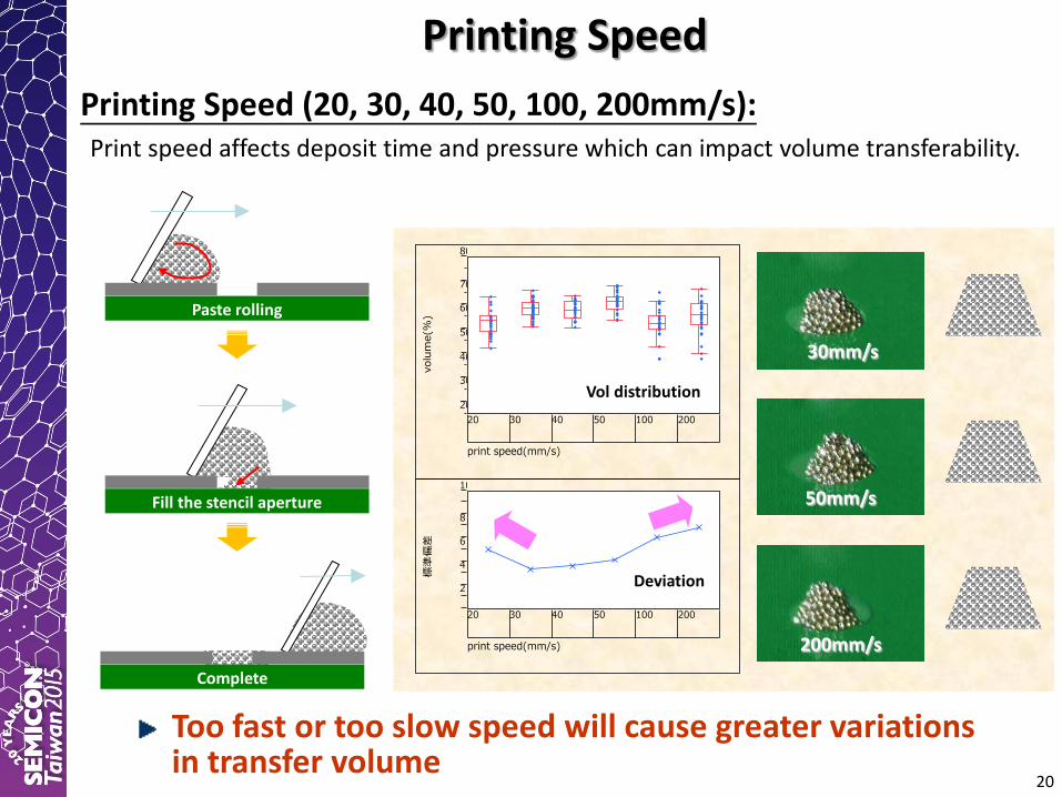
20
volu
me(
%)
20
30
40
50
60
70
80
20 30 40 50 100 200
print speed(mm/s)
標準
偏差
0
2
4
6
8
10
20 30 40 50 100 200
print speed(mm/s)
30mm/s
50mm/s
200mm/s
Too fast or too slow speed will cause greater variations in transfer volume
Printing Speed (20, 30, 40, 50, 100, 200mm/s): Print speed affects deposit time and pressure which can impact volume transferability.
Vol distribution
Deviation
Printing Speed
Complete
Paste rolling
Fill the stencil aperture

21
volu
me(
%)
20
30
40
50
60
70
80
0.1 0.5 1 5 10
down speed(mm/s)
標準
偏差
0
2
4
6
8
10
0.1 0.5 1 5 10
down speed(mm/s)
0.1mm/s
1mm/s
5mm/s
Vol distribution
Deviation
After Printing
During Release
Separation Speed (0.1, 0.5, 1.0, 2.5, 5.0, 10.0mm/sec): Separation speed affects the adhesion to the aperture walls which can significantly impact paste release & print definition
Key is to minimize solder buildup on walls
Slow separation speed can cause poor print definition and lower transfer volume, leading to larger variations
Separation Speed

22
Solder Paste Selection ・Solder Powder Size ・FLUX
Stencil Selection
Suitable Printing Parameters
Suitable Reflow Profile
Contents

23
Reflow Profile Guideline:
③
③ Ramp-to-peak ■ Recommended rate (avg): 2~3℃/s
④
①
② Preheat/Soak ■ Recommended temp: 140~170℃ ■ Recommended time: Around 70sec
④ Reflow ■ Recommended peak temp: 230~245℃ ■ Time above liquidus(220℃): Over 30sec
②
It is important to control preheat zone (where oxidation is likely to occur) and ramp-to-peak rate
① Ramp-to-soak ■ Recommended rate (avg): 2~4℃/s
Critical Parameters of Reflow Profile

24
are best possibilities
From solder paste approach…
- Jet Dispense Process -
When more solder volume is needed for larger components: When solder joint strength becomes a concern for larger devices,
■ Stencil design change ■ Chip solder
Process to supplement solder volume of printing paste Non-contact Shorter tact time as compared to air dispense
Half-edge (Step Down) Chip Solder
Mixed Component Mounting
Chip solder

25
Forc
e(N
)
0
10
20
30
40
50
60
0.12t 0.10t 0.08t 0.08t+Jet
Stencil thickness
Shear Strength by Print Thickness: Effects of strength by adding solder (1608 chip capacitor)
Stencil Thickness Avg Force (N)
0.12t 40.08
0.10t 33.13
0.08t 26.54
0.08t + JET 37.13
Adding solder volume by jet dispensing can potentially increase strength Due to new process, further verification testing is needed
Potential Increase in Strength by Jet Dispensing
*Solder Paste : Senju NXD900ZH series

26
To achieve successful Fine Pitch assembly:
Solder Paste Selection ■ Solder powder : Select fine powder (< Type 6: 5~15um) ■ Flux : Select high oxidation-resistance & high heat-resistance chemistries
Stencil Selection Select stencil with very smooth aperture walls Select aperture design with 2.0 or lower aspect ratio
Printing Parameter Setting Set suitable parameters (especially separation speed)
PCB Quality (Plating/Resist) Ensure there is no contamination of the plating and resist is aligned
Reflow Profile Set suitable preheat temp/time & ramp-up speed
For Fine Pitch assembly, it is essential to increase overall accuracy
Conclusion

27
http://www.senju-m.co.jp
THANK YOU