smart card reader interface with pwoer management - … sheets/atmel pdfs/at83c24...1...
TRANSCRIPT

1
4234C–SCR–04/04
Features• Smart Card Interface
– Compliance with ISO 7816, EMV2000, GIE-CB, GSM and WHQL StandardsCard Clock Stop High or Low for Card Power-down ModesSupport Synchronous Cards with C4 and C8 ContactsCard Detection and Automatic de-activation SequenceProgrammable Activation Sequence
– Direct Connection to the Smart CardLogic Level Shifters Short Circuit Current Limitation8kV+ ESD Protection (MIL/STD 883 Class 3)
– Programmable Voltage5V ±5% at 65 mA (Class A)3V ±0.2V at 65 mA (Class B)1.8V ±0.14V at 40 mA
– Low Ripple Noise: < 200 mV Max• Versatile Host Interface
– ICAM (Conditional Access) Compatible– Two Wire Interface (TWI) Link
Programmable Address Allow up to 8 Devices – Programmable Interrupt Output– Automatic Level Shifter (1.6V to VCC)
• Reset Output Includes– Power-On Reset (POR)– Power-Fail Detector (PFD)
• High-efficiency Step-up Converter: 80 to 98% Efficiency• Extended Voltage Operation: 2.85 to 5.5V • Low Power Consumption
– 1 mA Maximum Operating Current– 150 mA Maximum In-rush Current– 20 µA Typical Power-down Current (without Smart Card)
• 4 to 48 MHz Clock Input (7 MHz Min for Step-up Converter)• Industrial Temperature Range: -40 to +85°C• Packages: SO28 and QFN28
DescriptionThe AT83C24 is a smart card reader interface IC for smart card reader/writer applica-tions such as EFT/POS terminals and set top boxes. It enables the management ofany type of smart card from any kind of host. Up to 8 AT83C24 can be connected inparallel using the programmable TWI address.
Its high efficiency DC/DC converter, low quiescent current in standby mode makes itparticularly suited to low power and portable applications. The reduced bill of materialallows reducing significantly the system cost. A sophisticated protection system guar-antees timely and controlled shutdown upon error conditions.
Smart Card Reader Interface with Power Management
AT83C24

2 AT83C244234C–SCR–04/04
Acronyms TWI: Two-wire Interface
POR: Power On Reset
PFD: Power Fail Detect
ART: Automatic Reset Transition
ATR: Answer To Reset
Block Diagram
PRES/ INT
CLK
VSSVCC
CRST
CPRES
CIO, CC4, CC8
CCLK
CVCC
LI
RESET
Voltage supervisor POR/PFD
TWI Controller
Clocks Controller
DC/DCConverter
AnalogDrivers
SCL
SDA
I/O, C4, C8
DVCC
EVCC
A2, A1, A0, CMDVCC
Timer 16 Bits
Main Control& Logic Unit
CVSS

3
AT83C24
4234C–SCR–04/04
Pin Description
Pinout (Top View) AT83C24 28-pin SOIC Pinout QFN28 pinout
Note: NC = Not Connected
Signals
A1
A2
A0
1
EVCC
CCLK
CRST
SCL
VCC
RESET
CVSS
CVCCin
I/O
CLK
2
3 4
5
6
78
9
10
28
2726
25
24
23
22
21
20
19
LI
PRES/INTDVCC
VSS
SDA
CPRES
12
18
17
11
C8
CIO
C4
16
15
CC8
CMDVCC
CC4
1
VSSVCC
CVSS
LI
2
3
4 5
6
78 9 10 11 12 13 14
16
15
17
18
19
20
2122232425262728
TOP VIEW
QFN 28
CIO
CC
8
CVCCin
CR
ST
CP
RE
S
CC
4
CC
LK
CMDVCC
RE
SE
T
DV
CC
C8
CLK
PR
ES
/INT
C4
/CK/CK
/RST A0
/RST
/3V/3V
CVCCCVCC SDA
SCL
A1
A2
I/O
EVCC
13
14
NC
NC
NC
NC
Table 1. Ports Description
Pad Name Pad Internal
Power SupplyESD
LimitsPad Type Description
A2/CK-
A1/RST-
A0/3V
EVCC 3 kV I
Microcontroller Interface Function:
TWI bus slave address selection input.
A2 and A1 pins are respectively connected to CCLK and CRST signals in “transparent mode” (see Transparent mode § page 16).
The slave address of the device is based on the value present on A2, A1, A0 on the rising edge of RESET pin (see Table 2).
PRES/INT EVCC3 kV
O
open-drain
Microcontroller Interface Function:
Depending on IT_SEL value (see CONFIG4 register),
PRES/INT outputs card presence status or interruptions (see Interrupts § page 9)
An internal Pull-up to EVCC can be activated in the pad if necessary using INT_PULLUP bit (CONFIG4 register).
RESET VCC
3 kVI/O
open-drain
Microcontroller Interface Function:
• Power-on reset • A low level on this pin keeps the AT83C24 under reset even if applied on power-on.
It also resets the AT83C24 if applied when the AT83C24 is running.• Asserting RESET when the chip is in Shut-down mode returns the chip to normal
operation.• AT83C24 is driving the Reset pin Low on power-on-reset or if power fail on VCC or
DVCC (see POWERMON bit in CONFIG4 register), this can be used to reset or interrupt other devices. After reset, AT83C24 needs to be reconfigured before starting a new card session.
SDA VCC3 kV
I/O
open-drain
Microcontroller Interface Function
TWI serial data
SCL VCC3 kV
I/O
open-drain
Microcontroller Interface Function
TWI serial clock

4 AT83C244234C–SCR–04/04
I/O EVCC3 kV
I/O
Microcontroller Interface Function
Copy of CIO pin and high level reference for EVCC.
I/O is the reference level for EVCC after power up.
If an external power supply is on EVCC pin, I/O should not be kept above EVCC for an extended time.
C4 EVCC3 kV I/O
(pull-up)
Microcontroller Interface Function
Copy of Card CC4.
C8 EVCC3 kV I/O
(pull-up)
Microcontroller Interface Function
Copy of Card CC8.
CLK EVCC3 kV
IMicrocontroller Interface Function
Master Clock
CIO CVCC 8 kV+I/O
(pull-up)
Smart card interface function
Card I/O
CC4 CVCC 8 kV+I/O
(pull-up)
Smart card interface function
Card C4
CC8 CVCC 8 kV+I/O
(pull-up)
Smart card interface function
Card C8
CPRES VCC 8 kV+I
(pull-up)
Smart card interface function
Card presence
An internal Pull-up to VCC can be activated in the pad if necessary using PULLUP bit (CONFIG1 register).
CCLK CVCC 8 kV+ OSmart card interface function
Card clock
CRST CVCC 8 kV+ OSmart card interface function
Card reset
CMDVCC EVCC3 kV+
I
(pull-up)Microcontroller Interface Function:
Activation/Shutdown of the smart card Interface.
VCC 3 kV+ PWRSupply Voltage
VCC is used to power the internal voltage regulators and I/O buffers.
LI 3 kV+ PWR
DC/DC Input
LI must be tied to VCC pin through an external coil (typically 4.7 µH) and provides the current for the charge pump of the DC/DC converter.
It may be directly connected to VCC if the step-up converter is not used (see STEPREG in CONFIG4 register and see minimum VCC value in Table 16 (class A) and table 17 (class B)).
CVCC 8 kV+ PWR
Card Supply Voltage
CVCC is the programmable voltage output for the Card interface.
It must be connected to an external decoupling capacitor.
CVCCin 8 kV+ PWRCard Supply Voltage
This pin must be connected to CVCC.
Table 1. Ports Description (Continued)
Pad Name Pad Internal
Power SupplyESD
LimitsPad Type Description

5
AT83C24
4234C–SCR–04/04
DVCC 3 kV+ PWR
Digital Supply Voltage
Is internally generated and used to supply the digital core.
This pin has to be connected to an external capacitor of 100 nF and should not be connected to other devices.
EVCC 3 kV+ PWR
Extra Supply Voltage (Microcontroller power supply)
EVCC is used to supply the level shifters of host interface pins.
EVCC voltage can be supplied from the external EVCC pin.
It can also be generated internally by an automatic follow up of the logic high level on the I/O pin. In this configuration, connect a 100 nF + 100kOhms in parallel between EVCC pin and VSS pin.
CVSS 8 kV+ GNDDC/DC Ground
CVSS is used to sink high shunt currents from the external coil.
VSS GND Ground
Table 1. Ports Description (Continued)
Pad Name Pad Internal
Power SupplyESD
LimitsPad Type Description

6 AT83C244234C–SCR–04/04
Operational Modes
TWI Bus Control The Atmel Two-wire Interface (TWI) interconnects components on a unique two-wirebus, made up of one clock line and one data line with speeds of up to 400 Kbits per sec-ond, based on a byte-oriented transfer format.
The TWI-bus interface can be used:
– To configure the AT83C24
– To select the operating mode of the card: 1.8V, 3V or 5V
– To configure the automatic activation sequence
– To start or stop sessions (activation and de-activation sequences)
– To initiate a warm reset
– To control the clock to the card in active mode
– To control the clock to the card in stand-by mode (stop LOW, stop HIGH or running)
– To enter or leave the card stand-by or power-down modes
– To select the interface (connection to the host I/O/C4/C8)
– To request the status (card present or not, over-current and out of range supply voltage occurrence)
– To drive and monitor the card contacts by software
– To accurately measure the ATR delay when automatic activation is used
TWI Commands
Frame Structure The structure of the TWI bus data frames is made of one or a series of write and readcommands completed by STOP.
Write commands to the AT83C24 have the structure:
ADDRESS BYTE + COMMAND BYTE + DATA BYTE(S)
Read commands to the AT83C24 have the structure:
ADDRESS BYTE + DATA BYTE(S)
The ADDRESS BYTE is sampled on A2/CK, A1/RST, A0/3V after each reset(hard/soft/general call) but A2/CK, A1/RST, A0/3V can be used for transparent modeafter the reset.
Figure 1. Data transfer on TWI bus
SDA
SCL
start condition stop condition
1 2 3 4 5 6 7 8 9
acknowledgementfrom slave
Adresse byte commandand/or data

7
AT83C24
4234C–SCR–04/04
Address Byte The first byte to send to the device is the address byte. The device controls if the hard-ware address (A2/CK, A1/RST, A0/3V pins on reset) corresponds to the address givenin the address byte (A2, A1, A0 bits).
If the level is not stable on A2/CK pin (or A1/RST pin, or A0/3V pin) at reset, the userhas to send the commands to the possible address taken by the device.
Figure 2. Address Byte
Up to 8 devices can be connected on the same TWI bus. Each device is configured witha different combination on A2/CK, A1/RST, A0/3V pins. The address byte of eachdevice for read/write operations are listed below.
Table 2. Address Byte Values
A2(A2/CK pin)
A1(A1/RST pin)
A0(A0/3V pin)
Address Byte for
Read Command
Address Byte for
Write Command
0 0 0 0x41 0x40
0 0 1 0x43 0x42
0 1 0 0x45 0x44
0 1 1 0x47 0x46
1 0 0 0x49 0x48
1 0 1 0x4B 0x4A
1 1 0 0x4D 0x4C
1 1 1 0x4F 0x4E
b7 b6 b5 b4 b3 b2 b1 b0
0 01 0 A2 A1 A0 R/W
Slave Address on 7 Bits
1 for READ Command
0 for WRITE Command

8 AT83C244234C–SCR–04/04
Write Commands The write commands are:
1. Reset:
Initialize all the logic and the TWI interface as after a power-up or power-fail reset. Ifthe interface is activated, an emergency de-activation sequence is also performed.This is a one-byte command.
2. Write Config:
Configure the device according to the last six bits in the CONFIG0 register and tothe following four bytes in CONFIG1, CONFIG2, CONFIG3 then CONFIG4 regis-ters. This is a five bytes command.
Figure 3. Command byte format for Write CONFIG0 command
3. Write Timer:
Program the 16-bit automatic reset transition timer with the following two bytes. Thisis a three bytes command.
4. Write Interface:
Program the interface. This is a one-byte command. The MSB of the command byteis fixed at 0.
5. General Call Reset:
A general call followed by the value 06h has the same effect as a Reset command.
Table 3. Write Commands Description
Address Byte
(See Table 2) Command ByteData Byte 1
Data Byte 2
Data Byte 3
Data Byte 4
1. Reset 0100 XXX0 1111 1111
2. Write config0100 XXX0
(10 + CONFIG0 6 bits)
CONFIG1 CONFIG2 CONFIG3 CONFIG4
3. Write Timer 0100 XXX0 1111 1100 TIMER1 TIMER0
4. Write Interface0100 XXX0
(0+INTERFACE 7 bits)
5. General Call Reset
0000 0000 0000 0110
b7 b6 b5 b4 b3 b2 b1
1 X0 X X X X
CONFIG0 on 6 Bits
b0
X

9
AT83C24
4234C–SCR–04/04
Read Command After the slave address has been configured, the read command allows to read one orseveral bytes in the following order:
• STATUS, CONFIG0, CONFIG1, CONFIG2, CONFIG3, INTERFACE, TIMER1, TIMER0, CAPTURE1, CAPTURE0
• FFh is completing the transfer if the microcontroller attempts to read beyond the last byte.
Note: Flags are only reseted after the corresponding byte read has been acknowledged by themaster.
Table 4. Read Command Description
Interrupts The PRES/INT behavior depends on IT_SEL bit value (see CONFIG4 register).
• If IT_SEL= 0, the PRES/INT output is High by default. PRES/INT is driven Low by at least one of the following event:
– INSERT bit set in CONFIG0 register (card insertion/extraction or bit set by software )
– VCARD_INT bit set in STATUS register (the DC/DC output voltage has settled)
– over-current detection on CVCC
– VCARDERR bit set in CONFIG0 register (out of range voltage on CVCC or bit set by software)
– ATRERR bit set in CONFIG0 register (no ATR before the card clock counter overflows or bit set by software)
• If IT_SEL= 1 (for software compatibility with existing devices) the PRES/INT output is High to indicate a card is present and none of the following event has occured:
– over-current detection on CVCC
– VCARDERR bit set in CONFIG0 register (out of range voltage on CVCC or bit set by software)
– ATRERR bit set in CONFIG0 register (no ATR before the card clock counter overflows or bit set by software)
Byte Description Byte Value
Address byte 0100 XXX1
Data byte 1 STATUS
Data byte 2 CONFIG0
Data byte 3 CONFIG1
Data byte 4 CONFIG2
Data byte 5 CONFIG3
Data byte 6 CONFIG4
Data byte 7 INTERFACE
Data byte 8 TIMER 1 (MSB)
Data byte 9 TIMER 0 (LSB)
Data byte 10 CAPTURE 1 (MSB)
Data byte 11 CAPTURE 0 (LSB)
Data byte 12 0xFF

10 AT83C244234C–SCR–04/04
Several AT83C24 devices can share the same interrupt and the microcontroller canidentify the interrupt sources by polling the status of the AT83C24 devices using TWIcommands.
Clock Controller The clock controller outputs two clocks (as shown in Figure 4 and Figure 5):
1. a clock for the CCLK: Four different sources can be used: CLK pin, DCCLK sig-nal, CARDCK bit or A2/CK pin (in transparent mode).
Figure 4. Clock Block Diagram with Software Activation (see activation sequence §)
Figure 5. Clock Block Diagram with Hardware Activation (see activation sequence §)
CRST Controller The CRST output pin is driven by the A1/RST pin signal pin or by the CARDRST bitvalue. This selection depends of the CRST_SEL bit value (see CONFIG4 register).
If the CRST pin signal is driven by the CARDRST bit value, two modes are available:
• If the ART bit is reset, CRST pin is driven by CARDRST bit.
DCK[2:0]
CKS[2:0]
CLK
A2/CK CCLK
DC/DCDCCLK
0
1
CKSTOP bit
CARDCK bit
DCK[2:0]
CKS[2:0]
CLK
A2/CK CCLK
DC/DCDCCLK
0
1
CKSTOP bit
CARDCK bit
CMDVCC
A1/RST
CRST_SEL bit
Hardware activation

11
AT83C24
4234C–SCR–04/04
• If the ART bit is set, CRST pin is controlled and follows the “Automatic Reset Transition” (see Figure 12).
Figure 6. CRST Block Diagram with soft activation
Figure 7. CRST Block Diagram with Hardware Activation (CMDVCC pin used)
CIO, CC4, CC8 Controller The CIO, CC4, CC8 output pins are driven respectively by CARDIO, CARDC4,CARDC8 bits values or by I/O, C4, C8 signal pins. This selection depends of the IODISbit value. If IODIS is reset, data are bidirectional between respectively I/O, C4, C8 pinsand CIO, CC4, CC8 pins.
A1/RSTCRST0
1
CRST_SEL bit
0
1
ART bit
CARDRST bit tb delay
see Fig 12
A1/RSTCRST0
1
0
1
ART bit
CARDRST bit
CRST_SEL bit
Hardware activation
CMDVCC
activation
CMDVCC
deactivation

12 AT83C244234C–SCR–04/04
Figure 8. CIO, CC4, CC8 Block Diagram
IO Transceiver IO and CIO pins are linked together if IODIS bit=0 in INTERFACE register. This is doneautomatically during an hardware activation.
Their iddle level is 1.
The same behavior is applicable on C4/CC4 and C8/CC8 pins.
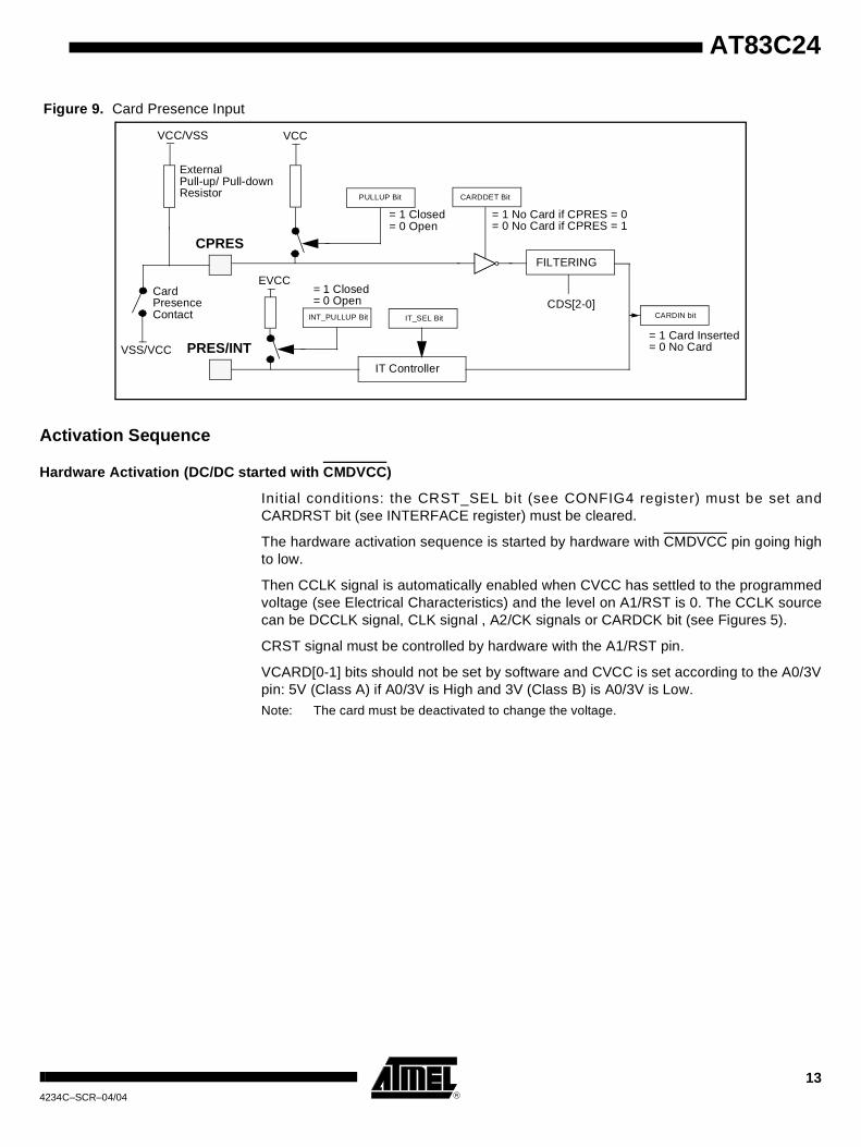
Card Presence Detection The card presence is provided by the CPRES pin. The polarity of card presence contactis selected with the CARDDET bit (see CONFIG1 register). A programmable filtering iscontrolled with the CDS[2-0] bits (see CONFIG1 register).
An internal pull-up on the CPRES pin can be disconnected in order to reduce the con-sumption, an external pull-up must then be connected to VCC. The PULLUP bit (seeCONFIG1 register) controls this feature.
If the card presence contact is connected to VCC, the internal pull-up must be discon-nected and an external pull-down must be connected to the CPRES pin. The cardpresence switch is usually connected to gnd. The CARDDET bit polarity is then inverted.
An interrupt can be generated if a card is inserted or extracted (see interrupts).
CIO
0
1
0
1CARDIO bit
CC4
CC80
1CARDC8 bit
IODIS bit
CARDC4 bit
I/O
C4
C8
13
AT83C24
4234C–SCR–04/04
Figure 9. Card Presence Input
Activation Sequence
Hardware Activation (DC/DC started with CMDVCC)
Initial conditions: the CRST_SEL bit (see CONFIG4 register) must be set andCARDRST bit (see INTERFACE register) must be cleared.
The hardware activation sequence is started by hardware with CMDVCC pin going highto low.
Then CCLK signal is automatically enabled when CVCC has settled to the programmedvoltage (see Electrical Characteristics) and the level on A1/RST is 0. The CCLK sourcecan be DCCLK signal, CLK signal , A2/CK signals or CARDCK bit (see Figures 5).
CRST signal must be controlled by hardware with the A1/RST pin.
VCARD[0-1] bits should not be set by software and CVCC is set according to the A0/3Vpin: 5V (Class A) if A0/3V is High and 3V (Class B) is A0/3V is Low.Note: The card must be deactivated to change the voltage.
PULLUP Bit CARDDET Bit
= 1 Closed = 0 Open
External Pull-up/ Pull-downResistor
Card Presence Contact
= 1 No Card if CPRES = 0 = 0 No Card if CPRES = 1
CARDIN bit
= 1 Card Inserted = 0 No Card
IT Controller
CPRES
PRES/INT
VCC/VSS
FILTERING
CDS[2-0]
VCC
VSS/VCC
INT_PULLUP Bit
= 1 Closed = 0 Open
EVCC
IT_SEL Bit

14 AT83C244234C–SCR–04/04
Figure 10. Activation sequence with CMDVCC
Software Activation (DC/DC Started With Writing in VCARD[1:0] bits) and ART bit = 1
The following sequence can be applied:
1. Card Voltage is set by software to the required value (VCARD[1:0] bits in CONFIG0 register). This writing starts the DC/DC.
2. Wait of the end of the DC/DC init with a polling on VCARDOK bit (STATUS register) or wait for PRES/INT to go Low if enabled (if IT_SEL bit = 0 in CONFIG4 register). When VCARDOK bit is set (by hardware), CARDIO bit should be set by software.
3. CKSTOP, IODIS are programmed by software. CKSTOP bit is reset to have the clock running. IODIS is reset to drive the I/O, C4, C8 pins and the CIO,CC4, CC8 pins according to each other.
4. CARDRST bit (see INTERFACE register) is set by software.
Automatic Reset Transition description:
A 16-bit counter starts when CARDRST bit is set. It counts card clock cycles. The CRSTsignal is set when the counter reaches the TIMER[1-0] value which corresponds to the“tb” time (Figure 5).The counter is reseted when the CRST pin is released and it isstopped at the first start bit of the Answer To Request (ATR) on CIO pin.
The CIO pin is not checked during the first 200 clock cycles (time on Figure 5). If theATR arrives before the counter reaches Timer[1-0] value, the activation sequence fails,the CRST signal is not set and the Capture[1-0] register contains the value of thecounter at the arrival of the ATR.
If the ATR arrives after the rising edge on CRST pin and before the card clock counteroverflows (65535 clock cycles), the activation sequence completes. The Capture[1-0]register contains the value of the counter at the arrival of the ATR (tc time on Figure 12).
CMDVCC
A1/RST
CCLK
CVCC
CRST
CIO

15
AT83C24
4234C–SCR–04/04
Figure 11. Software activation with ART bit = 1
ISO 7816 constraints: ta = 200 card clock cycles
400 card clock cycles< = tb
400 card clock cycles< = tc < = 40000 card clock cyclesNote: Timer[1-0] reset value is 400.
Software Activation (DC/DC Started by Writing in VCARD[1:0] bits) and ART bit = 0
The activation sequence is controlled by software using TWI commands, depending onthe cards to support. For ISO 7816 cards, the following sequence can be applied:
1. Card Voltage is set by software to the required value (VCARD[1:0] bits in CONFIG0 register). This writing starts the DC/DC.
2. Wait of the end of the DC/DC init with a polling on VCARDOK bit (STATUS register) or wait for PRES/INT to go Low if enabled (if IT_SEL bit = 0 in CONFIG4 register). When VCARDOK bit is set (by hardware), CARDIO bit should be set by software.
3. CKSTOP, IODIS are programmed by software. CKSTOP bit is reset to have the clock running. IODIS is reset to drive the I/O, C4, C8 pins and the CIO,CC4, CC8 pins according to each other.
4. CRST pin is controlled by software using CARDRST bit (see INTERFACE register).
CVCC
CRST
CCLK
tctb
ta
CIO
CARDRST bit set
1
2
34

16 AT83C244234C–SCR–04/04
Figure 12. Software activation without automatic control (ART bit = 0)
Note: It is assumed that initially VCARD[1:0], CARDCK, CARDIO and CARDRST bits arecleared, CKSTOP and IODIS are set (those bits are further explained in the registersdescription)
Note: The user should check the AT83C24 status and possibly resume the activation sequenceif one TWI transfer is not acknowledged during the activation sequence.
Deactivation Sequence The card automatic deactivation is triggered when one the following condition occurs:
• ICARDERR bit is set by hardware
• VCARDERR bit is set by hardware (or by software)
• INSERT is set and CARDIN is cleared (card extraction)
• SHUTDOWN is set by software
• CMDVCC goes from Low to High
• Power fail on VCC (see POWERMON bit in CONFIG4 register)
• Reset pin going low
It is a self-timed sequence which cannot be interrupted when started (see Figure 13).Each step is separated by a delay based on Td equal to 8 periods of the DC/DC clock,typically 2 to 2.4 µs:
1. T0: CARDRST is cleared, SHUTDOWN bit set.
2. T0 + 5 x Td:CARDCK is cleared, CKSTOP, CARDIO and IODIS are set.
3. T0 + 6 x Td: CARDIO is cleared.
4. T0 + 7 x Td: VCARD[1-0] = 00.
CVCC
CRST
CCLK
CIO
2
4
31
ATR

17
AT83C24
4234C–SCR–04/04
Figure 13. Deactivation Sequence
Notes: 1. Setting ICARDERR by software does not trigger a deactivation. VCARDERR can beused to deactivate the card by software.
Transparent Mode If the microcontroller outputs ISO 7816 signals, a transparent mode allows to connectRST/CLK and I/O/C4/C8 signals after an electrical level control. The AT83C24 levelshifters adapt the card signals to the smart card voltage selection.
The CRST and CCLK microcontroller signals can be respectively connected to theA1/RST and A2/CK pins.
The CRST_SEL bit (in CONFIG4 register) selects standard or transparent configurationfor the CRST pin. CKS in CONFIG2 allows to select standard or transparent configura-tion for the CCLK pin. So CCLK and CRST are independent. A2/CK to A0/3V inputsalways give the TWI address at reset. The A0/3V pin can be used for TWI addressingand easily connect two AT83C24 devices on the same TWI bus.
If A2/CK to A0/3V are tied to the host microcontroller and their reset values areunknown, a general call on the TWI bus allows to reset all the AT83C24 devices and settheir address after A2/CK to A0/3V are fixed.
CVCC
CRST
CCLK
CIO,
5 x Td Td Td
CC4, CC8

18 AT83C244234C–SCR–04/04
Figure 14. Transparent Mode Description
Power Modes Two power-down modes are available to reduce the AT83C24 power consumption (seeSTUTDOWN bit in CONFIG1 register and LP bits in CONFIG3 register).
To enter in the mode number 4 (see table 5), the sequence is the following:
– First select the Low-power mode by setting the LP bit
– The activation of the SHUTDOWN bit can then be done.
The AT83C24 exits Power-down if a software/hardware reset is done or if SHUTDOWNbit is cleared. The AT83C24 is then active immediately.
Either a hardware reset or a TWI command clearing the SHUTDOWN bit can cause anexit from Power-down. The internal registers retain their value during the shutdownmode.
In Power-down mode, the device is sleeping and waiting for a wake up condition.
To reduce power consumption, the User should stop the clock on the CLK input aftersetting the SHUTDOWN bit. The clock can be enabled again just before exiting SHUT-DOWN (at least 10 µs before a START bit on SDA).
CCLK
CRST
CIOI/O
A2/CK
A1/RST
AT83C24
SMART CARD
CRST
CCLK
CC4
Microcontroller
CC8
CIO
C4
C8
CC4
CC8
Table 5. Power Modes Description
Mode Number
Shutdown
Bit
Lp
Bit Result
Typical
Supply
Current Description
1 0 X No action 160 mA Step up mode: VCC = 2.85V, CVCC = 5V, Icvcc = 65mA
2 0 X No action TBD mA Regulator mode: VCC = 5.2V, CVCC = 5V, Icvcc = 65mA
3 1 0 Shutdown mode 90 µA The TWI interface of the AT83C24 is active but its analog blocs are switched off to reduce the consumption
4 1 1 Shutdown mode with low power mode
30 µA Pulsed mode of the internal 3V logic regulator

19
AT83C24
4234C–SCR–04/04
Power Monitoring The AT83C24 needs only one power supply to run: VCC.
If the microcontroller outputs signals with a different electrical level, the host positivesupply is connected to EVCC.
EVCC and VCC pins can be connected together if they have the same voltage.
• If EVCC and VCC have different electrical levels:
The EVCC pin and RESET pin should be connected with a resistor bridge. RESETpin high level must be higher than VIH (see Table 19). When EVCC drops, RESETpin level drops too. A deactivation sequence starts if a card was active.
Then the AT83C24 resets if RESET pin stays low.
• If EVCC and VCC have the same value, then they should be connected:
The AT83C24 integrates an internal 3V regulator to feed its logic from the VCC sup-ply. The bit powermon allows the user to select if the internal PFD monitors VCC orthe internal regulated 3V. If the PFD monitors VCC (POWERMON bit=0), a deacti-vation is performed if VCC falls below VPFDP (see VPFDP value in the datasheet).Same deactivation is performed if the internal 3V falls below VPFDP and POWER-MON bit = 1

20 AT83C244234C–SCR–04/04
RegistersTable 6. CONFIG0 (Config Byte 0)
7 6 5 4 3 2 1 0
1 0 ATRERR INSERT ICARDERR VCARDERR VCARD1 VCARD0
Bit Number Bit Mnemonic Description
7-6 1-0 These bits cannot be programmed and are read as 1-0.
5 ATRERR
Answer to Reset Interrupt
This bit is set when the card clock counter overflows (no falling edge on CIO is received before the overflow of the card clock counter).
This bit is cleared by hardware when this register is read. It can be set by software for test purpose. The reset value is 0.
4 INSERT
Card Insertion InterruptThis bit is set when a card is inserted or extracted: a change in CARDIN value filtered according to CDS[2-0]. After power up, if the level on CPRES pin is 0, then INSERT bit is set.
It can be set by software for test purpose.
This bit is cleared by hardware when this register is read. It cannot be cleared by software.
The reset value is 0.
3 ICARDERR
Card Over Current InterruptThis bit is set when an over current is detected on CVCC. It can be set by software for test purpose (no card deactivation is performed).
This bit is cleared by hardware when this register is read. It cannot be cleared by software.
The reset value is 0.
2 VCARDERR
Card Out of Range Voltage InterruptThis bit is set when the output voltage goes out of the voltage range specified by VCARD field. It can be set by software for test purpose and deactivate the card.
This bit is cleared by hardware when this register is read. It cannot be cleared by software.
The reset value is 0.
1-0 VCARD[1:0]
Card Voltage Selection
VCARD[1:0] = 00: 0V
VCARD[1:0] = 01: 1.8V
VCARD[1:0] = 10: 3V
VCARD[1:0] = 11: 5V
VCARD[1:0] writing to 1.8V, 3V, 5V starts the DC/DC if a card is detected.
VCARD[1:0] writing to 0 stops the DC/DC.
No card deactivation is performed when the voltage is changed between 1.8V, 3V or 5V. The microcontroller should deactivate the card before changing the voltage.
The reset value is 00.

21
AT83C24
4234C–SCR–04/04
Table 7. CONFIG 1 (Config Byte 1)
7 6 5 4 3 2 1 0
X ART SHUTDOWN CARDDET PULLUP CDS2 CDS1 CDS0
Bit Number
Bit Mnemonic Description
7 X This bit should not be set.
6 ART
Automatic Reset Transition
Set this bit to have the CRST pin changed according to activation sequence.
Clear this bit to have the CRST pin immediately following the value programmed in CARDRST.
The reset value is 0.
5 SHUTDOWN
Shutdown
Set this bit to reduce the power consumption. An automatic de-activation sequence will be done.
Clear this bit to enable VCARD[1:0] selection.
The reset value is 0.
4 CARDDET
Card Presence Detection Polarity
Set this bit to indicate the card presence detector is closed when no card is inserted (CPRES is low).
Clear this bit to indicate the card presence detector is open when no card is inserted (CPRES is high).Changing CARDDET will set INSERT bit (see CONFIG0) even if no card is inserted or extracted.
The reset value is 0.
3 PULLUP
Pull-up Enable
Set this bit to enable the internal pull-up on the CPRES pin. This allows to minimize the number of external components.
Clear this bit to disable the internal pull-up and minimize the power consumption when the card detection contact is on. Then an external pull-up must be connected to VCC (typically a 1 MΩ resistor).
The reset value is 1.
2-0 CDS[2:0]
Card Detection filtering
CPRES is sampled by the master clock provided on CLK input. A change on CPRES is detected after:
CDS[2-0] = 0: 0 sample(1)
CDS[2-0] = 1: 4 identical samples
CDS [2-0] = 2: 8 identical samples (reset value)
CDS[2-0] = 3: 16 identical samples
CDS[2-0] = 4: 32 identical samples
CDS[2-0] = 5: 64 identical samples
CDS[2-0] = 6: 128 identical samples
CDS[2-0] = 7: 256 identical samples
The reset value is 2.
Note: When CDS[2-0] = 0 and IT_SEL = 0, PRES/INT = 1 when nocard is present and PRES/INT = 0 when a card is insertedeven if CLK is STOPPED. This can be used to wake up theexternal microcontroller and restart CLK when a card isinserted in the AT83C24.If CDS[2-0] = 0, IT_SEL = 1 and CLK is stopped, a card insertion orextraction has no effect on PRES/INT pin.

22 AT83C244234C–SCR–04/04
Notes: 1. When this field is changed a special logic insures no glitch occurs on the CCLK pinand actual configuration changes can be delayed by half a period to two periods ofCCLK.
2. CCLK must be stopped with CKSTOP bit before switching from CKS = (0, 1, 2, 3, 6,7) to CKS = (4, 5) or vice versa.
3. When DCK = 0, a change on CKS as no effect.
Table 8. CONFIG2 (Config Byte 2)
7 6 5 4 3 2 1 0
X DCK2 DCK1 DCK0 X CKS2 CKS1 CKS0
Bit Number
Bit Mnemonic Description
7 X This bit should not be set.
6-4 DCK[2:0]
DC/DC Clock prescaler factor
DCCLK is the DC/DC clock. It is the division of CLK input by DCK prescaler.
DCK = 0: prescaler factor equals 1 (CLK = 4 to 4.61MHz)
DCK [2:0] = 1: prescaler factor equals 2 (CLK = 7 to 9.25MHz)
DCK [2:0] = 2: prescaler factor equals 4 (CLK = 14 to 18.5 MHz)
DCK [2:0] = 3: prescaler factor equals 6 (CLK = 21 to 27.6 MHz)
DCK [2:0] = 4: prescaler factor equals 8 (CLK = 28 to 34.8 MHz)
DCK [2:0] = 5: prescaler factor equals 10 (CLK = 35 to 43 MHz)
DCK [2:0] = 6: prescaler factor equals 12 (CLK = 43.1 to 48 MHz)
DCK [2:0] = 7: reserved
The reset value is 1.
DCCLK must be as close as possible to 3.68 MHz with a duty cycle of 50%. DCCLK must be programmed before to start the DC/DC.
The other values of CLK are not allowed.
DCK has to be properly configured before resetting the STEPREG bit.
3 X This bit should not be set.
2-0 CKS[2:0]
Card Clock prescaler factor
CKS [2:0] = 0: CCLK = CLK (then the maximum frequency on CLK is 24 MHz)
CKS [2:0] = 1: CCLK = DCCLK (DC/DC clock)
CKS [2:0] = 2: CCLK = DCCLK / 2
CKS [2:0] = 3: CCLK = DCCLK / 4
CKS [2:0] = 4: CCLK = A2
CKS [2:0] = 5: CCLK = A2 / 2
CKS [2:0] = 6: CCLK = CLK / 2
CKS [2:0] = 7: CCLK = CLK / 4
The reset value is 0.
23
AT83C24
4234C–SCR–04/04
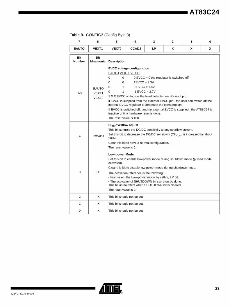
Table 9. CONFIG3 (Config Byte 3)
7 6 5 4 3 2 1 0
EAUTO VEXT1 VEXT0 ICCADJ LP X X X
Bit Number
Bit Mnemonic Description
7-5
EAUTO
VEXT1
VEXT0
EVCC voltage configuration:
EAUTO VEXT1 VEXT0
0 0 0 EVCC = 0 the regulator is switched off.
0 0 1EVCC = 2.3V
0 1 0 EVCC = 1.8V
0 1 1 EVCC = 2.7V
1 X X EVCC voltage is the level detected on I/O input pin.
if EVCC is supplied from the external EVCC pin, the user can switch off the internal EVCC regulator to decrease the consumption.
If EVCC is switched off, and no external EVCC is supplied, the AT83C24 is inactive until a hardware reset is done.
The reset value is 100.
4 ICCADJ
CICC overflow adjust
This bit controls the DC/DC sensitivity to any overflow current.
Set this bit to decrease the DC/DC sensitivity (CICC_ovf is increased by about 20%).
Clear this bit to have a normal configuration.
The reset value is 0.
3 LP
Low-power Mode
Set this bit to enable low-power mode during shutdown mode (pulsed mode activated).
Clear this bit to disable low-power mode during shutdown mode.
The activation reference is the following:• First select the Low-power mode by setting LP bit.• The activation of SHUTDOWN bit can then be done.This bit as no effect when SHUTDOWN bit is cleared.
The reset value is 0.
2 X This bit should not be set.
1 X This bit should not be set.
0 X This bit should not be set.

24 AT83C244234C–SCR–04/04
Table 10. CONFIG4 (Config Byte 4)
7 6 5 4 3 2 1 0
X X X STEPREG INT_PULLUP POWERMON IT_SEL CRST_SEL
Bit Number Bit Mnemonic Description
7-5 X-X-X These bits should not be set.
4 STEPREG
Step Regulator modeClear this bit to enable the automatic step-up converter (CVCC is stable even if VCC is not higher than CVCC).
Set this bit to permanently disable the step-up converter (CVCC is stable only if VCC is sufficiently higher than CVCC).
The reset value is 0.
This bit must always be set if no external self is used
3 INT_PULLUP
Internal pull-up
Set this bit to activate the internal pull-up (connected internally to EVCC) on PRES/INT pin.
Clear this bit to deactivate the internal pull-up.
The reset value is 0.
2 POWERMON
Power monitor
Set this bit so that the internal power monitor checks the Digital Supply Voltage (DVCC) of the AT83C24.
Clear this bit so that the internal power monitor checks the VCC of the AT83C24.
The reset value is 0.
1 IT_SEL
Interrupt Select
Set this bit to disable INSERT and VCARD_INT interrupts. Then PRES/INT is driven High when a card is present and no error is detected.
Clear this bit to have all the interrupt sources enabled and active Low. Then PRES/INT is an open-drain output with a programmable pull-up (see INT_PULLUP).
The reset value is 0.
0 CRST_SEL
Card Reset Selection
Set this bit to have the CRST pin driven by hardware through the A1 pin.
Clear this bit to have the CRST pin driven by software through the CARDRST bit.
The reset value is 0.

25
AT83C24
4234C–SCR–04/04
Table 11. INTERFACE (Interface Byte)
7 6 5 4 3 2 1 0
0 IODIS CKSTOP CARDRST CARDC8 CARDC4 CARDCK CARDIO
Bit Number Bit Mnemonic Description
7 0 This bit cannot be programmed and is read as 0.
6 IODIS
Card I/O isolation
Set this bit to drive the CIO, CC4, CC8 pins according to CARDIO, CARDC4, CARDC8 respectively and to put I/O, C4, C8 in Hi-Z. This can be used to have the I/O, and C4 and C8 pins of the host communicating with another AT83C24 interface, while CIO, CC4 and CC8 are driven by software (or if the card is in standby or power-down modes).
Clear this bit to drive the I/O/CIO, C4/CC4 and C8/CC8 pins according to each other. This can be used to activate asynchronous cards.
The reset value is 1.
5 CKSTOP
CARD Clock Stop
Set this bit to stop CCLK according to CARDCK. This can be used to set asynchronous cards in power-down mode (GSM) or to drive CCLK by software.
Clear this bit to have CCLK running according to CKS. This can be used to activate asynchronous cards.
Note: When this bit is changed a special logic ensures that no glitch occurs on the CCLK pin and actual con-figuration changes can be delayed by half a period to two periods of CCLK.
The reset value is 1.
4 CARDRST
Card Reset
Set this bit to enter a reset sequence according to ART bit value.
Clear this bit to drive a low level on the CRST pin.
The reset value is 0.
3 CARDC8
Card C8
Set this bit to drive the CC8 pin High with the on-chip pull-up (according to IODIS bit value). The pin can then be an input (read in STATUS register).
Clear this bit to drive a low level on the CC8 pin (according to IODIS bit value).
The reset value is 0.
2 CARDC4
Card C4
Set this bit to drive the CC4 pin High with the on-chip pull-up (according to IODIS bit value). The pin can then be an input (read in STATUS register).
Clear this bit to drive a low level on the CC4 pin (according to IODIS bit value).
The reset value is 0.
1 CARDCK
Card Clock
Set this bit to set a high level on the CCLK pin (according to CKSTOP bit value).
Clear this bit to drive a low level on the CCLK pin.
The reset value is 0.
0 CARDIO
Card I/O
Set this bit to drive the CIO pin High with the on-chip pull-up (according to IODIS bit value). The pin can then be an input (read in STATUS register).
Clear this bit to drive a low level on the CIO pin (according to IODIS bit value).The reset value is 0.

26 AT83C244234C–SCR–04/04
Reset value = 0x00000001
Table 12. STATUS (Status Byte)
7 6 5 4 3 2 1 0
CC8 CC4 CARDIN VCARDOK X VCARD_INT CRST CIO
Bit Number Bit Mnemonic Description
7 CC8
Card CC8
This bit provides the actual level on the CC8 pin when read.
The reset value is 0.
6 CC4
Card CC4
This bit provides the actual level on the CC4 pin when read.
The reset value is 0.
5 CARDINCard Presence Status
This bit is set when a card is detected.It is cleared otherwise.
4 VCARD_OK
Card Voltage Status
This bit is set by the DCDC when the output voltage remains within the voltage range specified by VCARD[1:0] bits.It is cleared otherwise.
The reset value is 0.
3 X This bit should not be set.
2 VCARD_INT
Card voltage interrupt
This bit is set when VCARD_OK bit is set.
This bit is cleared when read by the microcontroller.
The reset value is 0.
1 CRST
Card RST
This bit provides the actual level on the CRST pin when read.
The reset value is 0.
0 CIO
Card I/O
This bit provides the actual level on the CIO pin when read.
The reset value is 0.
Table 13. TIMER 1 (Timer MSB)
7 6 5 4 3 2 1 0
Bit 15 Bit 14 Bit 13 Bit 12 Bit 11 Bit 10 Bit 9 Bit 8
Bit Number
Bit Mnemonic Description
7 - 0 Bits 15 - 8 Timer MSB (bits 15 to 8)
27
AT83C24
4234C–SCR–04/04
Reset value = 0x10010000
Reset value = 0x00000000
Reset value = 0x00000000
Table 14. TIMER 0 (Timer LSB)
7 6 5 4 3 2 1 0
Bit 7 Bit 6 Bit 5 Bit 4 Bit 3 Bit 2 Bit 1 Bit 0
Bit Number
Bit Mnemonic Description
7 - 0 bits 7 - 0 Timer LSB (bits 7to 0)
Table 15. CAPTURE 1 (Capture MSB)
7 6 5 4 3 2 1 0
bit 15 bit 14 bit 13 bit 12 bit 11 bit 10 bit 9 bit 8
Bit Number
Bit Mnemonic Description
7 - 0 bits 15 - 8 See automatic activation sequence.
Table 16. CAPTURE 0 (Capture LSB)
7 6 5 4 3 2 1 0
bit 7 bit 6 bit 5 bit 4 bit 3 bit 2 bit 1 bit 0
Bit Number
Bit Mnemonic Description
7 - 0 bits 7 - 0 See automatic activation sequence (page 7).
28 AT83C244234C–SCR–04/04
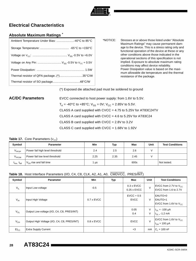
Electrical Characteristics
Absolute Maximum Ratings *
(*) Exposed die attached pad must be soldered to ground
AC/DC Parameters EVCC connected to host power supply: from 1.6V to 5.5V.
TA = -40°C to +85°C; VSS = 0V; VCC = 2.85V to 5.5V.
CLASS A card supplied with CVCC = 4.75 to 5.25V for AT83C24TV
CLASS A card supplied with CVCC = 4.6 to 5.25V for AT83C24
CLASS B card supplied with CVCC = 2.8V to 3.2V
CLASS C card supplied with CVCC = 1.68V to 1.92V
Ambient Temperature Under Bias: .....................-40°C to 85°C
Storage Temperature: ................................... -65°C to +150°C
Voltage on VCC: .......................................... VSS -0.5V to +6.0V
Voltage on Any Pin: .............................VSS -0.5V to VCC + 0.5V
Power Dissipation: .......................................................... 1.5W
Thermal resistor of QFN package..(*)............................35°C/W
Thermal resistor of SO package.................................48°C/W
*NOTICE: Stresses at or above those listed under “Absolute Maximum Ratings” may cause permanent dam-age to the device. This is a stress rating only and functional operation of the device at these or any other conditions above those indicated in the operational sections of this specification is not implied. Exposure to absolute maximum rating conditions may affect device reliability.Power Dissipation value is based on the maxi-mum allowable die temperature and the thermal resistance of the package.
Table 17. Core Parameters (VCC)
Symbol Parameter Min Typ Max Unit Test Conditions
VPFDP Power fail high level threshold 2.4 2.5 2.6 V
VPFDM Power fail low level threshold 2.25 2.35 2.45 V
trise, tfall VDD rise and fall time 1 µs 600s Not tested.
Table 18. Host Interface Parameters (I/O, C4, C8, CLK, A2, A1, A0, CMDVCC, PRES/INT)
Symbol Parameter Min Typ Max Unit Test Conditions
VIL Input Low-voltage -0.50.3 x EVCC
0.25 x EVCCV
EVCC from 2.7V to VCC
EVCC from 1.6 to 2.7V
VIH Input High Voltage 0.7 x EVCC
EVCC + 0.5
EVCC V
EAUTO=0
EAUTO=1
EVCC from 1.6V to VCC
VOL Output Low-voltage (I/O, C4, C8, PRES/INT)0.05
0.4
V
V
IOL = -100 µA
IOL = -1.2 mA
VOH Output High Voltage (I/O, C4, C8, PRES/INT) 0.8 x EVCC EVCC VEVCC from 1.6V to VCC
IOH = 100 µA
EICC Extra Supply Current +3 mA CL = 100 nF

29
AT83C24
4234C–SCR–04/04
RPRES/INT PRES/INT weak pull-up output current 300 330 360 κΩShort to VSS
INT_PULLUP = 0: Internal pull-up active.
EVCC EVCC pin not connected to a power supply Vpeak - 10 mV Vpeak Vpeak + 25 mV V
CL = 100 nF, EIcc = +3 mA
Vpeak on I/O from 1.6V to VCC
EAUTO = 1:
min duration 1µs,
min frequency 0.1Hz,
spikes <50ns are filtered.
EVCC EVCC pin connected to a power supplyVpeak - 200mV
EAUTO = 1
Table 18. Host Interface Parameters (I/O, C4, C8, CLK, A2, A1, A0, CMDVCC, PRES/INT) (Continued)
Symbol Parameter Min Typ Max Unit Test Conditions
Table 19. Host Interface DC Parameters (SCL, SDA, RESET)
Symbol Parameter Min Typ Max Unit Test Conditions
VIL Input Low-voltage -0.51.9
0.3 x VCCV
VCC > 4.5V
VCC <= 4.5V
VIH Input High Voltage2.85
0.7 x VCCVCC + 0.5 V
VCC > 4.5V
VCC <= 4.5V
VOL Output Low-voltage 0.4 V IOL = -3 mA
VHIST Input trigger hysteresis 0.1 x VCC
Table 20. Smart Card Class A DC Parameters
Symbol Parameter Min Typ Max Unit Test Conditions
CICCCard Supply Current Capability 65
65mA
VCC = 2.85V, STEPREG = 0
VCC = 5.35V, STEPREG = 1
CICC_ovf
Card Supply Current Overflow:
ICCADJ = 0 (reset value)
ICCADJ = 1
65
65
120
130
130
150
mA VCC from 2.85 to 5.5V
Ripple on CVCC60
150
200
350mV
0 < Icard < 60mA CL =10µF
0 < Icard < 65mA CL = 3.3µF
Spikes on CVCC 4.6 5.3 V
Max. charge 40 nA.s
Max. duration 400 ns
Max. Icard variation 200 mA
Vcardok up Vcardok high level threshold 4.8 4.9 V
Vcardok down Vcardok low level threshold4.6
4.75
4.8
4.8V
AT83C24
AT83C24TV
TVHL CVCC valid to 0180
500
250
750µs
Icard = 0, VCC > VPFDP
CL = 3.3 µF Icard = 0
CL = 10 µF Icard = 0
(see note 1)

30 AT83C244234C–SCR–04/04
Notes: 1. Capacitor: X7R type, max ESR value is 100mΩ
Notes: 1. Capacitor: X7R type or X5R type, max ESR value is 100mΩ
TVLH CVCC 0 to Valid
180
110
TBD
TBD
250
250
TBD
TBD
µs
VCC = 3V, CL = 3.3µF
Icard = 65mA AT83C24TV
Icard = 0mA AT83C24TV
VCC = 2.85V, CL = 10µF
Icard = 60mA AT83C24
Icard = 0mA AT83C24
Table 20. Smart Card Class A DC Parameters
Symbol Parameter Min Typ Max Unit Test Conditions
Table 21. Smart Card Class B DC Parameters
Symbol Parameter Min Typ Max Unit Test Conditions
CICC Card Supply Current Capability
65
65
65
65
mA
VCC = 5.5V, STEPREG = 0
VCC = 3V, STEPREG = 0
VCC = 2.85V, STEPREG = 0
VCC = 3.25V, STEPREG = 1
CICC_ovf
Card Supply Current Overflow:
ICCADJ = 0 (reset value)
ICCADJ = 1
0.065
0.065
0.13
0.14
0.14
0.15
A VCC from 3.0 to 5.5V
Ripple on CVCC 60200
350mV
0 < Icard < 65mA CL =10µF
0 < Icard < 65mA CL = 3.3µF
Spikes on CVCC 2.76 3.24 V
Maxi. charge 40 nA.s
Max. duration 400 ns
Max. variation Icard 200mA
Vcardok up Vcardok high level threshold 2.8 2.9 V
Vcardok down
Vcardok low level threshold 2.76 2.85 V
TVHL CVCC valid to 0130
TBD
250
TBDµs
Icard = 0, VCC > VPFDP
CL = 3.3 µF Icard = 0
CL = 10 µF Icard = 0
(see note 1)
TVLH CVCC 0 to Valid
140
110
130
100
250
250
250
250
µs
VCC = 3V, CL = 3.3µF
Icard = 65mA AT83C24TV
Icard = 0mA AT83C24TV
VCC = 2.85V, CL = 10µF
Icard = 60mA AT83C24
Icard = 0mA AT83C24

31
AT83C24
4234C–SCR–04/04
Note: Capacitor: X7R type, max ESR value is 100mΩ
Table 22. Smart Card C DC Parameters
Symbol Parameter Min Typ Max Unit Test Conditions
CICC Card Supply Current Capability
40
40
40
15
mA
VCC = 5.5V
VCC = 4V
VCC = 3V
VCC = 2.85V
CICC_ovf
Card Supply Current Overflow:
ICCADJ = 0 (reset value)
ICCADJ = 1
TBD
TBD
TBD
TBD
TBD
TBD
A
Spikes on CVCC TBD TBD V TBD
Vcardok up Vcardok high level threshold TBD TBD V
Vcardok down
Vcardok low level threshold TBD TBD V
TVHL CVCC valid to 0 TBD µsIcard = 0, CL = 10 µF(1)
CVCC = 1.8V to 0.4V
TVLH CVCC 0 to valid
TBD
TBD
TBD
TBD
µs
RL = 90ΩRL = 0
Icard = 0, CL = 10 µF(1)
CVCC = 0.4 to VCARDOK
Table 23. Smart Card Clock DC Parameters (CCLK pin)
Symbol Parameter Min Typ Max Unit Test Conditions
VOL Output Low-voltage 0 0.4 VIOL = -200 µA CLASS A&B&1.8V
VOH Output High Voltage
CVCC - 0.45
TBD
CVCC
TBD
VIOH = +200 µA CLASS A&B
CLASS 1.8V
IOS Short Circuit Current -30 30 mA Short to GND or CVCC
tR tF Rise and Fall time
16
22.5
TBDns
CL = 30 pF CLASS A
CL = 30 pF CLASS B
CLASS 1.8V
Rise and Fall Slew rate
0.2
0.12
TBD
V/ns
CLASS A
CCLK from 0.5 to 4.2V
CLASS B
CCLK from 0.5 to 0.85 x CVCC
CLASS 1.8V
Low level voltage stability-0.25
TBD
0.5
TBDV
CLASS A&B
CLASS 1.8V

32 AT83C244234C–SCR–04/04
High level voltage stability
CVCC-0.5
CVCC-0.4
TBD
CVCC+0.25
CVCC+0.25
TBD
V
CVCC = CLASS A
CVCC = CLASS B
CLASS 1.8V
Table 23. Smart Card Clock DC Parameters (CCLK pin) (Continued)
Symbol Parameter Min Typ Max Unit Test Conditions
Table 24. Smart Card I/O DC Parameters (CIO, CC4, CC8 pins)
Symbol Parameter Min Typ Max Unit Test Conditions
VIL Input Low-voltage -0.3V 0.8 V IIL = 500 µA
IIL Input Low Current 700 µA CVCC = CLASS A&B&1.8
VIH Input High Voltage0.6 x CVCC
0.7 x CVCC
CVCC
CVCCV
CVCC = CLASS A
CVCC = CLASS B & 1.8V
IIH Input High Current -20 +20 µA
VOL Output Low-voltage 0
0.45
0.3
TBD
V
IOL = -1 mA CLASS A
IOL = -1 mA CLASS B
IOL = -1 mA CLASS 1.8V
VOH Output High Voltage0.75 x CVCC
0.9 x CVCC
CVCC
CVCCV
IOH = 40 µA CLASS A&B&1.8V
IOH = 0µA, CLASS A&B
IOS Output Short Circuit Current -15 +15 mA Short to GND or CVCC
Low level voltage stability
-0.25
-0.25
TBD
0.6
0.4
TBD
V
CLASS A
CLASS B
CLASS 1.8V
High level voltage stability CVCC-0.5 CVCC+0.25 V CVCC = CLASS A&B&1.8
tR tFRise and Fall time
0.1 µS
CL = 65 pF
CLASS A:
0.6V <--> 0.7 x CVCC
CLASS B & 1.8V:
0.4V <--> 0.7 x CVCC
Table 25. Smart Card RST DC Parameters (CRST pin)
Symbol Parameter Min Typ Max Unit Test Conditions
VOL Output Low-voltage0
0
0.12 x CVCC
0.4V
IOL = -20 µA CLASS A&B&1.8V
IOL = -200 µA CLASS A&B&1.8V
VOH Output High Voltage CVCC - 0.45 CVCC VIOH = 200 µA
CLASS A&B&1.8V
IOS Output High Current -15 +15 mA Short to GND or CVCC
tR tF Rise and Fall time 0.1 µs CL = 30pF
Low level voltage stability -0.25
0.5V
0.3V
TBD
V
CLASS A
CLASS B
CLASS 1.8V

33
AT83C24
4234C–SCR–04/04
High level voltage stability
CVCC-0.5
CVCC-0.4
TBD
CVCC+0.25 V
CLASS A
CLASS B
CLASS 1.8V
Table 25. Smart Card RST DC Parameters (CRST pin) (Continued)
Symbol Parameter Min Typ Max Unit Test Conditions
Table 26. Card Presence DC Parameters
Symbol Parameter Min Typ Max Unit Test Conditions
RCPRES CPRES weak pull-up output current 300 330 360 κΩShort to VSS
PULLUP = 1:
Internal pull-up active

34 AT83C244234C–SCR–04/04
Typical Application
Figure 1. Typical Standard Mode Application Diagram
Note: 1. The external resistor on I/O can be removed if the C51 pin has an internal resistor.
100nF
XTAL1 XTAL2
+10uF
C51
VSS VSS
100nF
VSS
C1
C2 C3
4.7µH
VSS VSS
Card 0
PRES/INT
CLK
VS
S
VC
C
CRST
CPRESCIO, CC4, CC8
CCLK
CVCC
LI
CV
SS
AT83C24SCLSDA
I/O, C4, C8
PRES/INT
CLK
VS
S
VC
C
CRST
CPRESCIO, CC4, CC8
CCLK
CVCC
LI
CV
SS
AT83C24SCLSDA
I/O, C4, C8
PRES/INT
CLK
VS
S
VC
C
CRST
CPRESCIO, CC4, CC8
CCLK
CVCC
LI
CV
SS
AT83C24SCLSDA
I/O, C4, C8
Card 1
Card n
VCC
MICROCONTROLLER
TWI
INT0Px.y
100nF
CVSS
C44.7µH
VCC
100nF
CVSS
C74.7µH
VCC
L1
L2
L
RESETRST
VCC
4 to 48 MHz RESET
RESET
VCC
VSS
VCC
VSS
VCC
A2
A1
A0
A2
A1
A0
A2
A1
A0
EVCC
EV
CC
EV
CC
EV
CC
EVCC
EVCC
VSS
DVCC
VSS
DVCC
VSS
DVCC
100nF
VSSC5
+10uF
VSSC6
100nF
VSSC8
+10uF
VSSC9
100nF
100nF
100nF
Note
VCC

Ordering Information
Part Number Supply Voltage Temperature Range Package Packing Product Marking
AT83C24-PRTIL(2) 2.85V to 5.5V Industrial QFN28 Tray AT83C24IL
AT83C24-PRRIL(2) 2.85V to 5.5V Industrial QFN28 Tape&Reel AT83C24IL
AT83C24-PRTIM(2) 4.00V to 5.5V Industrial QFN28 Tray AT83C24IM
AT83C24-PRRIM(2) 4.00V to 5.5V Industrial QFN28 Tape&Reel AT83C24IM
AT83C24-TISIL 2.85V to 5.5V Industrial SO28 Stick AT83C24IL
AT83C24-TIRIL 2.85V to 5.5V Industrial SO28 Tape&Reel AT83C24IL
AT83C24-TISIM 4.00V to 5.5V Industrial SO28 Stick AT83C24IM
AT83C24-TIRIM 4.00V to 5.5V Industrial SO28 Tape&Reel AT83C24IM
AT83C24TV-PRTIL (1)(2) 2.85V to 5.5V Industrial QFN28 Tray AT83C24IL
AT83C24TV-PRRIL (1)(2) 2.85V to 5.5V Industrial QFN28 Tape&Reel AT83C24IL
AT83C24TV-PRTIM (1)(2) 4.00V to 5.5V Industrial QFN28 Tray AT83C24IM
AT83C24TV-PRRIM (1)(2) 4.00V to 5.5V Industrial QFN28 Tape&Reel AT83C24IM
AT83C24TV-TISIL (1) 2.85V to 5.5V Industrial SO28 Stick AT83C24IL
AT83C24TV-TIRIL (1) 2.85V to 5.5V Industrial SO28 Tape&Reel AT83C24IL
AT83C24TV-TISIM (1) 4.00V to 5.5V Industrial SO28 Stick AT83C24IM
AT83C24TV-TIRIM (1) 4.00V to 5.5V Industrial SO28 Tape&Reel AT83C24IM
LEAD FREE/HALOGEN FREE:
AT83C24-PRTUL(2) 2.85V to 5.5V Industrial QFN28 Tray AT83C24UL
AT83C24-PRRUL(2) 2.85V to 5.5V Industrial QFN28 Tape&Reel AT83C24UL
AT83C24-PRTUM(2) 4.00V to 5.5V Industrial QFN28 Tray AT83C24UM
AT83C24-PRRUM(2) 4.00V to 5.5V Industrial QFN28 Tape&Reel AT83C24UM
AT83C24-TISUL 2.85V to 5.5V Industrial SO28 Stick AT83C24UL
AT83C24-TIRUL 2.85V to 5.5V Industrial SO28 Tape&Reel AT83C24UL
AT83C24-TISUM 4.00V to 5.5V Industrial SO28 Stick AT83C24UM
AT83C24-TIRUM 4.00V to 5.5V Industrial SO28 Tape&Reel AT83C24UM
AT83C24TV-PRTUL (1)(2) 2.85V to 5.5V Industrial QFN28 Tray AT83C24UL
AT83C24TV-PRRUL (1)(2) 2.85V to 5.5V Industrial QFN28 Tape&Reel AT83C24UL
AT83C24TV-PRTUM(1)(2) 4.00V to 5.5V Industrial QFN28 Tray AT83C24UM

36 AT83C244234C–SCR–04/04
Note: 1. Enhanced AC/DC parameters.
2. Marking on package rotated starting March, 2004. Please refer to index mark for proper placement of chip.
AT83C24TV-PRRUM (1)(2) 4.00V to 5.5V Industrial QFN28 Tape&Reel AT83C24UM
AT83C24TV-TISUL (1) 2.85V to 5.5V Industrial SO28 Stick AT83C24UL
AT83C24TV-TIRUL (1) 2.85V to 5.5V Industrial SO28 Tape&Reel AT83C24UL
AT83C24TV-TISUM (1) 4.00V to 5.5V Industrial SO28 Stick AT83C24UM
AT83C24TV-TIRUM (1) 4.00V to 5.5V Industrial SO28 Tape&Reel AT83C24UM
Part Number Supply Voltage Temperature Range Package Packing Product Marking

37
AT83C24
4234C–SCR–04/04
Package Drawings
QFN28

38 AT83C244234C–SCR–04/04
SO28

39
AT83C24
4234C–SCR–04/04
Datasheet Change Log
Changes from 4234A-05/03 to 4234B-02/04
1. Addition of CRST, CIO, CCLK controllers descriptions, page 10.
2. Update of Hardware\Software activation description, page 13.
3. Suppression of low voltage regulator mode for power down modes, page 18.
4. Modification of clock values in CONFIG2 regsiter, page 22.
5. Addition of a point on QFN pinout view, page2.
6. Update of electrical characteristics, page 28.
Changes from 4234B-02/04 to 4234C - 04/04
1. Addition of references in ordering information
2. Update of EVCC description
3. Update of CARDDET bit and INSERT bit description

Printed on recycled paper.
Disclaimer: Atmel Corporation makes no warranty for the use of its products, other than those expressly contained in the Company’s standardwarranty which is detailed in Atmel’s Terms and Conditions located on the Company’s web site. The Company assumes no responsibil ity for anyerrors which may appear in this document, reserves the right to change devices or specifications detailed herein at any time without notice, anddoes not make any commitment to update the information contained herein. No licenses to patents or other intellectual property of Atmel aregranted by the Company in connection with the sale of Atmel products, expressly or by implication. Atmel’s products are not authorized for useas critical components in life support devices or systems.
Atmel Corporation Atmel Operations
2325 Orchard ParkwaySan Jose, CA 95131Tel: 1(408) 441-0311Fax: 1(408) 487-2600
Regional Headquarters
EuropeAtmel SarlRoute des Arsenaux 41Case Postale 80CH-1705 FribourgSwitzerlandTel: (41) 26-426-5555Fax: (41) 26-426-5500
AsiaRoom 1219Chinachem Golden Plaza77 Mody Road TsimshatsuiEast KowloonHong KongTel: (852) 2721-9778Fax: (852) 2722-1369
Japan9F, Tonetsu Shinkawa Bldg.1-24-8 ShinkawaChuo-ku, Tokyo 104-0033JapanTel: (81) 3-3523-3551Fax: (81) 3-3523-7581
Memory2325 Orchard ParkwaySan Jose, CA 95131Tel: 1(408) 441-0311Fax: 1(408) 436-4314
Microcontrollers2325 Orchard ParkwaySan Jose, CA 95131Tel: 1(408) 441-0311Fax: 1(408) 436-4314
La ChantrerieBP 7060244306 Nantes Cedex 3, FranceTel: (33) 2-40-18-18-18Fax: (33) 2-40-18-19-60
ASIC/ASSP/Smart CardsZone Industrielle13106 Rousset Cedex, FranceTel: (33) 4-42-53-60-00Fax: (33) 4-42-53-60-01
1150 East Cheyenne Mtn. Blvd.Colorado Springs, CO 80906Tel: 1(719) 576-3300Fax: 1(719) 540-1759
Scottish Enterprise Technology ParkMaxwell BuildingEast Kilbride G75 0QR, Scotland Tel: (44) 1355-803-000Fax: (44) 1355-242-743
RF/AutomotiveTheresienstrasse 2Postfach 353574025 Heilbronn, GermanyTel: (49) 71-31-67-0Fax: (49) 71-31-67-2340
1150 East Cheyenne Mtn. Blvd.Colorado Springs, CO 80906Tel: 1(719) 576-3300Fax: 1(719) 540-1759
Biometrics/Imaging/Hi-Rel MPU/High Speed Converters/RF Datacom
Avenue de RochepleineBP 12338521 Saint-Egreve Cedex, FranceTel: (33) 4-76-58-30-00Fax: (33) 4-76-58-34-80
Web Sitehttp://www.atmel.com
4234C–SCR–04/04 /xM
© Atmel Corporation 2004. All rights reserved. Atmel® and combinations thereof, are the registered trademarks of Atmel Corporation or its
subsidiaries. Other terms and product names may be the trademarks of others.