smart and high-performance digital-to-analog converters ...high-performance digital-to-analog...
TRANSCRIPT

Smart and high-performance digital-to-analog converterswith dynamic-mismatch mappingCitation for published version (APA):Tang, Y. (2010). Smart and high-performance digital-to-analog converters with dynamic-mismatch mapping.Eindhoven: Technische Universiteit Eindhoven. https://doi.org/10.6100/IR685413
DOI:10.6100/IR685413
Document status and date:Published: 01/01/2010
Document Version:Publisher’s PDF, also known as Version of Record (includes final page, issue and volume numbers)
Please check the document version of this publication:
• A submitted manuscript is the version of the article upon submission and before peer-review. There can beimportant differences between the submitted version and the official published version of record. Peopleinterested in the research are advised to contact the author for the final version of the publication, or visit theDOI to the publisher's website.• The final author version and the galley proof are versions of the publication after peer review.• The final published version features the final layout of the paper including the volume, issue and pagenumbers.Link to publication
General rightsCopyright and moral rights for the publications made accessible in the public portal are retained by the authors and/or other copyright ownersand it is a condition of accessing publications that users recognise and abide by the legal requirements associated with these rights.
• Users may download and print one copy of any publication from the public portal for the purpose of private study or research. • You may not further distribute the material or use it for any profit-making activity or commercial gain • You may freely distribute the URL identifying the publication in the public portal.
If the publication is distributed under the terms of Article 25fa of the Dutch Copyright Act, indicated by the “Taverne” license above, pleasefollow below link for the End User Agreement:
www.tue.nl/taverne
Take down policyIf you believe that this document breaches copyright please contact us at:
providing details and we will investigate your claim.
Download date: 24. Feb. 2020

Smart and High-Performance Digital-to-AnalogConverters with Dynamic-Mismatch Mapping
Yongjian Tang
Invitation
to the public defense ofmy PhD thesis entitled:
Smart andHigh-PerformanceDigital-to-AnalogConverters with
Dynamic-MismatchMapping
on Wednesday,October 6, 2010
at 16:00 hrsin Auditorium 4,
Eindhoven Universityof Technology.
You are cordially invitedto the reception that
will follow the defense.
Yongjian [email protected]
Smart and H
igh-Performance D
igital-to-Analog C
onverters with D
ynamic-M
ismatch M
apping - Yongjian Tang


Smart and High-Performance Digital-to-Analog Converters
with Dynamic-Mismatch Mapping
Yongjian Tang

This work was supported by the Foundation for Technical Sciences (STW), the Nether-
lands, under project 06655.
This work was cooperated with NXP Semiconductors, Central R&D, Mixed-Signal
Circuit and System Group.
Cover designed by Jing Zhang and Yongjian Tang.
Front cover:
Chip micrograph of the work presented in this thesis
Back cover:
QR code of the author’s signature

Smart and High-Performance Digital-to-Analog Converters
with Dynamic-Mismatch Mapping
PROEFSCHRIFT
ter verkrijging van de graad van doctor aan de
Technische Universiteit Eindhoven, op gezag van de
rector magnificus, prof.dr.ir. C.J. van Duijn, voor een
commissie aangewezen door het College voor
Promoties in het openbaar te verdedigen
op woensdag 6 oktober 2010 om 16.00 uur
door
Yongjian Tang
geboren te Rugao, China

Dit proefschrift is goedgekeurd door de promotor:
prof.dr.ir. A.H.M. van Roermund
Copromotor:
dr.ir. J.A. Hegt
Yongjian Tang
Smart and High-Performance Digital-to-Analog Converters with Dynamic-Mismatch
Mapping / Proefschrift Technische Universiteit Eindhoven, 2010.
A catalogue record is available from the Eindhoven University of Technology Library
ISBN: 978-90-386-2322-1
NUR 959
Key words: digital-to-analog converter / mismatch / calibration / correction / map-
ping / zero-IF receiver
All rights reserved
c©2010 Yongjian Tang, Eindhoven
No part of this publication may be reproduced or transmitted in any
form or by any means, electronic, mechanical, including photocopy, recording,
or any information storage and retrieval system without the
prior written permission of the copyright owner.

To my parents and Jing

Samenstelling van de promotiecommissie:
prof.dr.ir. A.C.P.M. Backx, Technische Universiteit Eindhoven, voorzitter
prof.dr.ir. A.H.M. van Roermund, Technische Universiteit Eindhoven, promotor
dr.ir. J.A. Hegt, Technische Universiteit Eindhoven, co-promotor
prof.dr.ir. G. Gielen, Katholieke Universiteit Leuven
prof.ir. A.J.M. van Tuijl, Universiteit Twente
prof.dr. J. Pineda de Gyvez, Technische Universiteit Eindhoven/NXP Semiconductors
prof.dr.ir. A.B. Smolders, Technische Universiteit Eindhoven
dr. K. Doris, NXP Semiconductors

Contents
Symbols and Abbreviations xi
1 Introduction 1
1.1 Motivation . . . . . . . . . . . . . . . . . . . . . . . . . . . . . . . . . 1
1.2 Thesis Aim and Outline . . . . . . . . . . . . . . . . . . . . . . . . . . 2
2 Digital-to-Analog Converters 5
2.1 Introduction to DACs . . . . . . . . . . . . . . . . . . . . . . . . . . . 5
2.1.1 Time Domain Response . . . . . . . . . . . . . . . . . . . . . . 5
2.1.2 Frequency Domain Response . . . . . . . . . . . . . . . . . . . 7
2.1.3 Applications . . . . . . . . . . . . . . . . . . . . . . . . . . . . 8
2.2 Performance Specifications . . . . . . . . . . . . . . . . . . . . . . . . . 8
2.2.1 Static Performance (DC) Specifications . . . . . . . . . . . . . 9
2.2.1.1 Offset and Gain Errors . . . . . . . . . . . . . . . . . 9
2.2.1.2 Integral Non-Linearity (INL) . . . . . . . . . . . . . . 10
2.2.1.3 Differential Non-Linearity (DNL) . . . . . . . . . . . . 10
2.2.2 Dynamic Performance (AC) Specifications . . . . . . . . . . . . 10
2.2.2.1 Single-tone SFDR/THD/NSD/SNR/SNDR . . . . . . 10
2.2.2.2 Two-tone Intermodulation Distortion (IMD) . . . . . 11
2.3 Architectures . . . . . . . . . . . . . . . . . . . . . . . . . . . . . . . . 12
2.3.1 Binary Architecture . . . . . . . . . . . . . . . . . . . . . . . . 12
2.3.2 Thermometer (Unary) Architecture . . . . . . . . . . . . . . . 13
2.3.3 Segmented Architecture . . . . . . . . . . . . . . . . . . . . . . 14
2.4 Physical Implementations . . . . . . . . . . . . . . . . . . . . . . . . . 14
2.4.1 Resistor DAC . . . . . . . . . . . . . . . . . . . . . . . . . . . . 14
2.4.2 Capacitor DAC . . . . . . . . . . . . . . . . . . . . . . . . . . . 15
2.4.3 Current-Steering DAC (CS-DAC) . . . . . . . . . . . . . . . . . 16
2.5 State of The Art . . . . . . . . . . . . . . . . . . . . . . . . . . . . . . 17
2.6 Conclusions . . . . . . . . . . . . . . . . . . . . . . . . . . . . . . . . . 20
3 Modeling and Analysis of Performance Limitations in CS-DACs 21
3.1 Static Mismatch Error . . . . . . . . . . . . . . . . . . . . . . . . . . . 22
3.1.1 Error Source: Amplitude Error . . . . . . . . . . . . . . . . . . 22
3.1.2 Effect on Static Performance . . . . . . . . . . . . . . . . . . . 24
3.1.3 Effect on Dynamic Performance . . . . . . . . . . . . . . . . . . 25
i

CONTENTS
3.1.3.1 Single-Tone SFDR/THD vs. Frequencies with Fixed
Amplitude Error . . . . . . . . . . . . . . . . . . . . . 25
3.1.3.2 Single-Tone SFDR/THD vs. Amplitude Error with
Fixed fs . . . . . . . . . . . . . . . . . . . . . . . . . 29
3.2 Dynamic Mismatch Error . . . . . . . . . . . . . . . . . . . . . . . . . 31
3.2.1 Error Sources: Amplitude & Timing Errors . . . . . . . . . . . 31
3.2.1.1 Introduction to Timing Error . . . . . . . . . . . . . . 32
3.2.1.2 Single-Tone SFDR/THD vs. Frequencies with Fixed
Timing Error . . . . . . . . . . . . . . . . . . . . . . . 35
3.2.1.3 Single-Tone SFDR/THD vs. Timing Error with Fixed
fs . . . . . . . . . . . . . . . . . . . . . . . . . . . . . 42
3.2.2 Dynamic Mismatch in Frequency Domain . . . . . . . . . . . . 44
3.2.3 New Parameters to Evaluate Dynamic Matching: Dynamic-
DNL & Dynamic-INL . . . . . . . . . . . . . . . . . . . . . . . 46
3.2.4 Comparison to Traditional Static DNL & INL . . . . . . . . . . 49
3.3 Non-Mismatch Error . . . . . . . . . . . . . . . . . . . . . . . . . . . . 51
3.3.1 Sampling Jitter . . . . . . . . . . . . . . . . . . . . . . . . . . . 51
3.3.2 Common Duty-Cycle Error . . . . . . . . . . . . . . . . . . . . 56
3.3.3 Finite Output Impedance . . . . . . . . . . . . . . . . . . . . . 61
3.3.4 Data-Dependent Switching Interference . . . . . . . . . . . . . 65
3.4 Summary of Performance Limitations . . . . . . . . . . . . . . . . . . 66
3.5 Conclusions . . . . . . . . . . . . . . . . . . . . . . . . . . . . . . . . . 68
4 Design Techniques for High-Performance Intrinsic and Smart CS-
DACs 71
4.1 Introduction to Smart DACs . . . . . . . . . . . . . . . . . . . . . . . 71
4.2 Design Techniques for Intrinsic DACs . . . . . . . . . . . . . . . . . . 73
4.2.1 Non-Mismatch-Error Focused Techniques . . . . . . . . . . . . 74
4.2.1.1 Sampling Jitter . . . . . . . . . . . . . . . . . . . . . 74
4.2.1.2 Common Duty-Cycle Error . . . . . . . . . . . . . . . 75
4.2.1.3 Finite Output Impedance . . . . . . . . . . . . . . . . 76
4.2.1.4 Data-Dependent Switching Interference . . . . . . . . 78
4.2.1.5 Design Techniques for Multiple Non-Mismatch Errors 79
4.2.2 Mismatch-Error Focused Techniques . . . . . . . . . . . . . . . 80
4.3 Design Techniques for Smart DACs . . . . . . . . . . . . . . . . . . . . 82
4.3.1 Analog Calibration Techniques . . . . . . . . . . . . . . . . . . 83
4.3.1.1 Techniques for Non-Mismatch Errors . . . . . . . . . 83
4.3.1.2 Techniques for Mismatch Errors . . . . . . . . . . . . 84
ii

CONTENTS
4.3.2 Digital Calibration Techniques . . . . . . . . . . . . . . . . . . 85
4.3.2.1 Digital vs. Analog Calibration Techniques . . . . . . . 85
4.3.2.2 Existing Digital Calibration Techniques: Mapping . . 86
4.3.2.3 A Novel Multi-Dimensional Mapping Technique: Dynamic-
Mismatch Mapping . . . . . . . . . . . . . . . . . . . 89
4.4 Summary of Design Techniques for Intrinsic and Smart DACs . . . . . 90
4.5 Conclusions . . . . . . . . . . . . . . . . . . . . . . . . . . . . . . . . . 93
5 A Novel Digital Calibration Technique: Dynamic-Mismatch Map-
ping (DMM) 95
5.1 Theory of Dynamic-Mismatch Mapping . . . . . . . . . . . . . . . . . 95
5.2 Measurement of Dynamic-Mismatch Error . . . . . . . . . . . . . . . . 99
5.2.1 Measurement Flow . . . . . . . . . . . . . . . . . . . . . . . . . 99
5.2.2 Sine-Wave Demodulation vs. Square-Wave Demodulation . . . 105
5.2.3 Weight Function between Amplitude and Timing Errors . . . . 107
5.3 Theoretical Evaluation of DMM . . . . . . . . . . . . . . . . . . . . . . 109
5.3.1 Effect of fm on Performance Improvement . . . . . . . . . . . . 110
5.3.2 Robustness of DMM . . . . . . . . . . . . . . . . . . . . . . . . 117
5.3.3 Application of DMM and Comparison to Other Techniques . . 119
5.4 Conclusions . . . . . . . . . . . . . . . . . . . . . . . . . . . . . . . . . 121
6 An On-chip Dynamic-Mismatch Sensor Based on a Zero-IF Receiver123
6.1 Architecture Considerations . . . . . . . . . . . . . . . . . . . . . . . . 123
6.2 Analog Front-end Design . . . . . . . . . . . . . . . . . . . . . . . . . . 125
6.2.1 Circuit Design . . . . . . . . . . . . . . . . . . . . . . . . . . . 125
6.2.1.1 Measurement Loading . . . . . . . . . . . . . . . . . . 125
6.2.1.2 Mixer . . . . . . . . . . . . . . . . . . . . . . . . . . . 127
6.2.1.3 Filter & Gain Stage: Trans-Impedance Amplifier . . . 128
6.2.2 Signal Transfer Function . . . . . . . . . . . . . . . . . . . . . . 129
6.2.3 Noise Analysis . . . . . . . . . . . . . . . . . . . . . . . . . . . 133
6.2.3.1 Noise Sources . . . . . . . . . . . . . . . . . . . . . . . 133
6.2.3.2 Noise Magnification Due to SC Effect . . . . . . . . . 135
6.2.3.3 Non-overlap LO vs. Overlap LO . . . . . . . . . . . . 138
6.3 ADC Design . . . . . . . . . . . . . . . . . . . . . . . . . . . . . . . . . 139
6.4 Overall Performance . . . . . . . . . . . . . . . . . . . . . . . . . . . . 139
6.5 Conclusions . . . . . . . . . . . . . . . . . . . . . . . . . . . . . . . . . 140
iii

7 Design Example 141
7.1 Overview . . . . . . . . . . . . . . . . . . . . . . . . . . . . . . . . . . 141
7.2 A 14-bit 650MS/s Intrinsic DAC Core . . . . . . . . . . . . . . . . . . 143
7.2.1 Circuit Design . . . . . . . . . . . . . . . . . . . . . . . . . . . 143
7.2.2 Experimental Results . . . . . . . . . . . . . . . . . . . . . . . 145
7.2.3 Comparison to Other Works . . . . . . . . . . . . . . . . . . . . 146
7.3 A 14-bit 200MS/s Smart DAC with DMM . . . . . . . . . . . . . . . . 148
7.3.1 Circuit Design . . . . . . . . . . . . . . . . . . . . . . . . . . . 148
7.3.2 Experimental Results . . . . . . . . . . . . . . . . . . . . . . . 150
7.3.2.1 Improvement on Static Performance . . . . . . . . . . 150
7.3.2.2 Improvement on Dynamic Performance . . . . . . . . 151
7.3.3 Benchmark . . . . . . . . . . . . . . . . . . . . . . . . . . . . . 156
7.4 Conclusions . . . . . . . . . . . . . . . . . . . . . . . . . . . . . . . . . 159
8 Conclusions 161
Reference 163
List of Publications 171
Summary 173
Samenvatting 175
Acknowledgment 179
Biography 181

List of Figures
1.1 Thesis outline . . . . . . . . . . . . . . . . . . . . . . . . . . . . . . . . 3
2.1 DAC in a wireless transceiver . . . . . . . . . . . . . . . . . . . . . . . 6
2.2 Magnitude of frequency responses of ideal NRZ and RZ DACs . . . . . 7
2.3 Application examples of Digital-to-Analog converters . . . . . . . . . . 8
2.4 DC specs of a DAC . . . . . . . . . . . . . . . . . . . . . . . . . . . . . 9
2.5 An example of DAC output spectrum . . . . . . . . . . . . . . . . . . 11
2.6 Graphic representation of IM3 and ACLR . . . . . . . . . . . . . . . . 12
2.7 A 4-bit binary-coded DAC example . . . . . . . . . . . . . . . . . . . . 13
2.8 A 4-bit thermometer-coded DAC example . . . . . . . . . . . . . . . . 13
2.9 A 5-bit 3T-2B segmented DAC example . . . . . . . . . . . . . . . . . 14
2.10 A 5-bit R-2R ladder DAC example . . . . . . . . . . . . . . . . . . . . 15
2.11 A 5-bit switched-cap DAC example . . . . . . . . . . . . . . . . . . . . 15
2.12 A 5-bit 3T-2B segmented current-steering DAC example . . . . . . . . 16
2.13 State-of-the-art DACs: sampling frequency versus technology node . . 19
2.14 State-of-the-art DACs: SFDR at very low signal frequencies (near DC)
versus static ENOB . . . . . . . . . . . . . . . . . . . . . . . . . . . . 19
2.15 State-of-the-art DACs: SFDR at high signal frequencies (near Nyquist)
versus input signal frequency . . . . . . . . . . . . . . . . . . . . . . . 20
3.1 Static Mismatch Error . . . . . . . . . . . . . . . . . . . . . . . . . . . 22
3.2 Amplitude error with the same fifs
at different fs . . . . . . . . . . . . 25
3.3 Amplitude error at the DAC output . . . . . . . . . . . . . . . . . . . 26
3.4 Simulated power distribution of amplitude errors, mean value of 200
samples . . . . . . . . . . . . . . . . . . . . . . . . . . . . . . . . . . . 27
3.5 THD vs. normalized input signal frequency at 500MS/s. σamp=0.2%.
Bars: one sigma spread (200 samples) . . . . . . . . . . . . . . . . . . 28
3.6 SFDR vs. normalized input signal frequency at 500MS/s. σamp=0.2%.
Bars: one sigma spread (200 samples) . . . . . . . . . . . . . . . . . . 28
3.7 SFDR vs. normalized input signal frequency at different sampling fre-
quency, σamp=0.2%. Bars: one sigma spread (200 samples) . . . . . . 29
3.8 SFDR vs. normalized input signal frequency with different σamp, 500MS/s 30
3.9 THD vs. normalized input signal frequency with different σamp, 500MS/s 30
3.10 Actual and simplified pulses . . . . . . . . . . . . . . . . . . . . . . . . 31
3.11 Equivalent timing error in the rising edge of a current cell . . . . . . . 32
3.12 Amplitude and timing (delay & duty-cycle) errors . . . . . . . . . . . 33
v

LIST OF FIGURES
3.13 Error sources of the delay error . . . . . . . . . . . . . . . . . . . . . . 34
3.14 A duty-cycle error caused by a threshold mismatch between differential
switches . . . . . . . . . . . . . . . . . . . . . . . . . . . . . . . . . . . 34
3.15 Timing error pulses . . . . . . . . . . . . . . . . . . . . . . . . . . . . . 35
3.16 Frequency response of first-difference analog and digital differentiators 36
3.17 Equivalent timing error per transition ∆teq,nTs , 200 samples . . . . . . 37
3.18 Simplification of original timing error pulses . . . . . . . . . . . . . . . 38
3.19 Simulated power distribution of timing error pulses, mean value of 200
samples . . . . . . . . . . . . . . . . . . . . . . . . . . . . . . . . . . . 39
3.20 THD, SFDR vs. normalized input signal frequency at 500MS/s, σtiming=5ps.
Bars: one sigma spread (200 samples) . . . . . . . . . . . . . . . . . . 40
3.21 THD vs. normalized input signal frequency at different sampling fre-
quencies, σtiming=5ps (200 samples) . . . . . . . . . . . . . . . . . . . 41
3.22 SFDR vs. normalized input signal frequency at different sampling fre-
quencies, σtiming=5ps (200 samples) . . . . . . . . . . . . . . . . . . . 42
3.23 THD vs. normalized input signal frequency with different σtiming at
500MS/s (200 samples) . . . . . . . . . . . . . . . . . . . . . . . . . . 43
3.24 SFDR vs. normalized input signal frequency with different σtiming at
500MS/s (200 samples) . . . . . . . . . . . . . . . . . . . . . . . . . . 43
3.25 Modulated rectangular output of current cells . . . . . . . . . . . . . . 45
3.26 Dynamic mismatch in I-Q plane (for clarity, axis are not to scale) . . . 46
3.27 One-dimensional static transfer curve of the static DAC output . . . . 47
3.28 Two-dimensional dynamic transfer curve of the fundamental component
of the modulated DAC output . . . . . . . . . . . . . . . . . . . . . . . 48
3.29 dynamic-DNL, dynamic-INL vs. modulation frequency fm . . . . . . . 50
3.30 Sampling Jitter . . . . . . . . . . . . . . . . . . . . . . . . . . . . . . . 51
3.31 Jitter effect on the SNR of RZ and NRZ DACs . . . . . . . . . . . . . 54
3.32 Common duty-cycle error . . . . . . . . . . . . . . . . . . . . . . . . . 57
3.33 SFDR/HD2 vs. input signal frequency with different common duty-
cycle errors at 200MS/s . . . . . . . . . . . . . . . . . . . . . . . . . . 59
3.34 SFDR/HD2 vs. normalized signal frequency with different sampling
frequencies, Dcom=1ps . . . . . . . . . . . . . . . . . . . . . . . . . . . 60
3.35 Input-signal dependent output impedance . . . . . . . . . . . . . . . . 61
3.36 Minimal Ro required for -90dBc IM3 with different thermometer bit N 63
3.37 HD3 and IM3 caused by finite output impedance versus fi . . . . . . . 64
3.38 Switching Interference . . . . . . . . . . . . . . . . . . . . . . . . . . . 65
3.39 Typical limitations on the DAC linearity by various error sources (fixed
sampling frequency) . . . . . . . . . . . . . . . . . . . . . . . . . . . . 67
vi

LIST OF FIGURES
4.1 Architecture of smart DACs . . . . . . . . . . . . . . . . . . . . . . . . 72
4.2 Multi-stage clocked-latches to minimize the jitter generation . . . . . . 75
4.3 CML logic vs. CMOS logic . . . . . . . . . . . . . . . . . . . . . . . . 75
4.4 Simple cascoding . . . . . . . . . . . . . . . . . . . . . . . . . . . . . . 76
4.5 Half-cell circuit at M2 on/off state . . . . . . . . . . . . . . . . . . . . 77
4.6 Always-on cascoding . . . . . . . . . . . . . . . . . . . . . . . . . . . . 78
4.7 Constant Switching Scheme . . . . . . . . . . . . . . . . . . . . . . . . 79
4.8 Harmonic Suppression . . . . . . . . . . . . . . . . . . . . . . . . . . . 80
4.9 Spectrum spreading by DEM . . . . . . . . . . . . . . . . . . . . . . . 82
4.10 Crossover-point control technique . . . . . . . . . . . . . . . . . . . . . 83
4.11 Analog calibration techniques for the amplitude error . . . . . . . . . . 85
4.12 Example of static-mismatch mapping (SMM) . . . . . . . . . . . . . . 87
5.1 SFDR and THD with five randomly chosen switching sequences of
MSBs for the same DAC . . . . . . . . . . . . . . . . . . . . . . . . . . 96
5.2 Dynamic mismatch in time, frequency and I-Q domain . . . . . . . . . 97
5.3 Dynamic-Mismatch Mapping . . . . . . . . . . . . . . . . . . . . . . . 99
5.4 I/Q demodulation by a sine-wave LO . . . . . . . . . . . . . . . . . . . 100
5.5 I/Q demodulation by a square-wave LO . . . . . . . . . . . . . . . . . 103
5.6 Plots of Efm and Eodd by sweeping φLO . . . . . . . . . . . . . . . . . 105
5.7 Efm and Eodd of current cells 1 to 10, measured with sine- or square-
wave demodulation at different φLO . . . . . . . . . . . . . . . . . . . 106
5.8 I/Q plots and optimized switching sequences at different fm . . . . . . 108
5.9 Evaluation process for DMM . . . . . . . . . . . . . . . . . . . . . . . 110
5.10 Dynamic-INL/dynamic-DNL improved by DMM with different fm . . 111
5.11 SFDR/THD improvement by DMM with different fm (fs=500MHz) . 112
5.12 HD2/HD3 improvement by DMM with different fm (fs=500MHz) . . 117
5.13 SFDR improvement by DMM with fm=50MHz at different fs . . . . . 118
5.14 THD improvement by DMM with fm=50MHz at different fs . . . . . 119
5.15 Performance pyramid of design techniques . . . . . . . . . . . . . . . . 120
6.1 Architecture of the proposed dynamic-mismatch sensor . . . . . . . . . 124
6.2 Function-block diagram of the dynamic-mismatch sensor . . . . . . . . 125
6.3 Measurement output network and measurement loading . . . . . . . . 126
6.4 Gilbert active Mixer and passive Mixer . . . . . . . . . . . . . . . . . . 127
6.5 Passive Mixer terminated by a TIA . . . . . . . . . . . . . . . . . . . . 128
6.6 Trans-impedance amplifier (TIA) . . . . . . . . . . . . . . . . . . . . . 129
6.7 OTA and buffer . . . . . . . . . . . . . . . . . . . . . . . . . . . . . . . 130
vii

6.8 Circuit diagram of the proposed dynamic-mismatch sensor . . . . . . . 130
6.9 Single-ended circuit model of the analog front-end before frequency
translation . . . . . . . . . . . . . . . . . . . . . . . . . . . . . . . . . . 131
6.10 Calculated and simulated signal transfer function . . . . . . . . . . . . 132
6.11 Simulated I/Q measurement results of the analog front-end (fm=50MHz)133
6.12 Simulated noise performance and noise sources . . . . . . . . . . . . . 134
6.13 Noise transfer analysis of the OTA noise . . . . . . . . . . . . . . . . . 137
6.14 Simulated and calculated noise amplification factor due to SC effect for
OTA . . . . . . . . . . . . . . . . . . . . . . . . . . . . . . . . . . . . . 138
6.15 Non-overlap LO . . . . . . . . . . . . . . . . . . . . . . . . . . . . . . . 139
7.1 Proposed DAC architecture with two modes . . . . . . . . . . . . . . . 142
7.2 Die photo . . . . . . . . . . . . . . . . . . . . . . . . . . . . . . . . . . 142
7.3 Block diagram of the intrinsic DAC . . . . . . . . . . . . . . . . . . . . 143
7.4 CML Master and slave latches . . . . . . . . . . . . . . . . . . . . . . 144
7.5 LVDS interface and CMOS2CML converter . . . . . . . . . . . . . . . 144
7.6 Measured THD of the intrinsic DAC at 650MS/s . . . . . . . . . . . . 145
7.7 Measured SFDR of the intrinsic DAC at 650MS/s . . . . . . . . . . . 146
7.8 SFDR of the intrinsic DAC core compared to state-of-the-art DACs . 147
7.9 Architecture of the proposed smart DAC with DMM . . . . . . . . . . 149
7.10 Mapping engine . . . . . . . . . . . . . . . . . . . . . . . . . . . . . . . 149
7.11 Measured INL and DNL for 14-bit accuracy . . . . . . . . . . . . . . . 150
7.12 Measured IM3 and NSD at 200MS/s . . . . . . . . . . . . . . . . . . . 152
7.13 Measured SFDR and THD at 200MS/s . . . . . . . . . . . . . . . . . . 153
7.14 DAC output spectrum with fi=95.4MHz @200MS/s . . . . . . . . . . 154
7.15 DAC output spectrum with proposed DMM at fi=95.4MHz @200MS/s 155
7.16 SFDR comparison with state-of-the-art CMOS DACs at similar fs . . 156
7.17 Comparison of SFDR at near-DC fi versus static ENOB . . . . . . . . 158
7.18 Comparison of SFDR at near-Nyquist fi . . . . . . . . . . . . . . . . . 158

List of Tables
2.1 State-of-the-art Nyquist DACs . . . . . . . . . . . . . . . . . . . . . . 18
3.1 Summary of the effect of amplitude errors on the DAC performance . 30
3.2 Summary of the effect of timing error on the performance of NRZ DACs 43
3.3 Summary of jitter effects on DACs and ADCs . . . . . . . . . . . . . . 55
3.4 Summary of the effect of the common duty-cycle error on the dynamic
performance . . . . . . . . . . . . . . . . . . . . . . . . . . . . . . . . . 61
3.5 Comparison between static mismatch and dynamic mismatch . . . . . 68
4.1 Summary of advanced design techniques for intrinsic DACs . . . . . . 81
4.2 Existing analog calibration techniques for amplitude errors . . . . . . 84
4.3 Summary of existing static-mismatch mapping techniques (SMM) . . . 88
4.4 Comparison of digital calibration techniques for mismatch errors . . . 90
4.5 Summary of emerging design techniques for high-performance intrinsic
and smart DACs . . . . . . . . . . . . . . . . . . . . . . . . . . . . . . 91
5.1 Existing analog calibration techniques for amplitude errors . . . . . . 109
5.2 Dynamic-INL improvement by DMM with different fm . . . . . . . . . 115
5.3 Dynamic-DNL improvement by DMM with different fm . . . . . . . . 115
5.4 SFDR improvement by DMM with different fm . . . . . . . . . . . . . 116
5.5 THD improvement by DMM with different fm . . . . . . . . . . . . . 116
6.1 Comparison between Gilbert and passive mixers . . . . . . . . . . . . 127
6.2 Transfer mechanism of noise sources to the output of the analog front-end136
6.3 Simulated performance summary of the proposed dynamic-mismatch
sensor . . . . . . . . . . . . . . . . . . . . . . . . . . . . . . . . . . . . 140
7.1 Performance summary of the 14b 650MS/s intrinsic DAC core . . . . . 147
7.2 DAC Performance summary with dynamic-mismatch mapping (DMM) 155
7.3 Benchmarking . . . . . . . . . . . . . . . . . . . . . . . . . . . . . . . . 157
ix


List of Symbols and Abbreviations
Symbol Description Unit
ADC Analog-to-digital converter
CML Current-mode logic
Dcom Common duty-cycle error seconds
DAC Digital-to-analog converter
DEM Dynamic element matching
DMM Dynamic-mismatch mapping
DNL Differential non-linearity LSB
Dynamic-DNL Dynamic differential non-linearity LSB
Dynamic-DNL Dynamic integral non-linearity LSB
DSP Digital signal processor
ENOB Effective number of bits bit
fi Input signal frequency Hz
fm Modulation or measurement frequency Hz
fs Sampling frequency Hz
IM3 Third-order intermodulation dBc
IMD Intermodulation distortion dBc
INL Integral non-linearity LSB
LO Local oscillator
LVDS Low-voltage differential signaling
NRZ Non-return-to-zero
NSD Noise power spectral density dBm/Hz
OTA Operational transconductance amplifier
RZ Return-to-zero
SFDR Spurious-free dynamic range dB
SMM Static-mismatch mapping
SNR Signal-to-noise ratio dB
SNDR Signal-to-(noise+distorion) ratio dB
TIA Trans-impedance amplifier
THD Total harmonic distortion dBc
Ts Sampling period seconds
ZOH Zero-order-hold
xi

Symbols and Abbreviations
Zout Output impedance Ω
σamp Deviation of Gaussian distributed amplitude errors %
σtiming Deviation of Gaussian distributed timing errors seconds
σjitter Deviation of Gaussian distributed jitter seconds
xii

1Introduction
1.1 Motivation
Since the invention of the first semiconductor transistor in the 1940s and the break-
through in the 1960s, microelectronics has been one of the most rapidly developed
technologies in the past few decades. The advanced microelectronics techniques, such
as integrated circuits (ICs), dramatically reformed our daily life and scientific research,
such as space technique, sensing technique, telecommunications, computer science and
multimedia entertainment.
As technology is moving to deep sub-micron or even nanometer scale, the com-
plementary metal-oxide-semiconductor (CMOS) technology has become the dominant
manufacturing technology for microelectronics in very large scale integration (VLSI)
applications. Digital integrated circuits directly benefit from this CMOS technology
scaling, since the minimal gate length of the transistor has a scaling factor of 0.7
from generation to generation (e.g. 0.18µm→0.13µm→90nm→65nm). This scaling
to ever smaller dimensions leads to higher transistor-integration density, faster circuit
speed, lower power dissipation and significantly reduced cost per function. As a result,
nowadays, more and more signal processing is preferred to be performed in the digi-
tal domain by digital signal processors (DSPs). This trend significantly increases the
demand for high quality interface circuits between analog and digital domain. Data
converters, i.e. Analog-to-Digital converters (ADCs) and Digital-to-Analog convert-
ers (DACs), as essential devices in interface circuits, are required to achieved high
1

CHAPTER 1. INTRODUCTION
performance with increased signal and sampling frequencies. In many emerging ap-
plications, such as wide-band or software-defined multi-mode communications, ADCs
and DACs are already one of the major performance bottlenecks of the whole system.
The research on high-speed high-performance data converters has become one of the
key topics in microelectronics, in both academia and industry.
1.2 Thesis Aim and Outline
The aim of this thesis is to develop design techniques for high-speed high-performance
smart DACs, especially designing a DAC with high dynamic performance, e.g. high
linearity, is the main concern of this work. The work focuses on Nyquist DACs with
current-steering architecture since that is the most suitable topology for high speed ap-
plications. For investigating fundamental performance limitations, the effect of various
error sources need to be analyzed. Based on that outcome, smart design techniques
can be developed to overcome technology limitations so that a high performance can
be achieved.
Figure 1.1 shows the outline of this thesis. Chapter 2 covers the basics of Nyquist
DACs, such as the definition, performance specifications, architectures and physical
implementations. Recently published state-of-the-art Nyquist DACs are also summa-
rized in that chapter.
In chapter 3, mismatch and non-mismatch errors are analyzed to investigate their
influence on the performance of current-steering DACs. In the signal frequency range
from DC to a few hundreds of MHz, mismatch errors, such as amplitude and tim-
ing errors, are typically the dominant error sources in the linearity of a DAC. As
signal and sampling frequencies increase, the effect of timing errors becomes more
and more dominant than that of amplitude errors. Traditional integral-nonlinearity
(INL) and differential-nonlinearity (DNL) are based on the static matching behavior
between current cells, i.e. only based on amplitude errors. In chapter 3, two new
parameters, named dynamic-INL and dynamic-DNL, are introduced to evaluate the
dynamic matching behavior between current cells. Compared to traditional static INL
and DNL, dynamic-INL and dynamic-DNL include both amplitude and timing errors,
resulting in a new methodology to improve the performance of DACs.
Chapter 4 introduces the concept of smart DACs. A smart DAC is an intrin-
sic DAC with additional techniques to acquire actual chip information and improve
the performance, yield, reliability or flexibility. Existing design techniques for high-
performance intrinsic and smart DACs are categorized and discussed.
Based on the concept of the dynamic-INL, chapter 5 introduces a novel digital cal-
ibration technique, called dynamic-mismatch mapping (DMM), to correct the effect of
2

1.2. THESIS AIM AND OUTLINE
both amplitude and timing errors in a digital way. Theoretical proofs of the proposed
DMM technique are given with dedicated explanations. The application of the DMM
technique and the comparison to other calibration techniques are also discussed in
chapter 5. Since the proposed DMM technique requires the dynamic-mismatch errors
to be accurately measured, an on-chip dynamic-mismatch sensor is designed in chapter
6. In order to verify the proposed DMM technique, chapter 7 gives a design example
of a 14-bit current-steering DAC. The silicon experimental results of a 14-bit 650MS/s
intrinsic DAC core and a 14-bit 200MS/s smart DAC with DMM are demonstrated.
Benchmark comparison shows that this design achieves state-of-the-art performance.
Finally, conclusions are drawn in chapter 8.
Figure 1.1: Thesis outline
3


2Digital-to-Analog Converters
IN this chapter, the concept and performance specifications of digital-to-analog con-
verters (DACs) are reviewed. Different DAC architectures and physical implemen-
tations are introduced. Recently published state-of-the-art DACs are summarized to
show the performance limitations.
2.1 Introduction to DACs
In this section, the general function and applications of digital-to-analog converters
(DACs) are briefly discussed.
2.1.1 Time Domain Response
In electronics, a Digital-to-Analog Converter (DAC) is a device that converts a finite-
precision digital-format number (the input, typically a finite-length binary-format
number) to an analog electrical quantity (such as voltage, current or electric charge).
Nowadays, with the development of digital technologies, for easy storage and process-
ing, most analog signals are digitized by Analog-to-Digital converters (ADCs) and are
processed by digital signal processors (DSPs) [1]. However, our perceptual world is
still analog so that the digital signal has to be converted back into analog domain
such that, for example, the data can be transmitted with high signal quality in com-
munication systems or a human being can hear a music or watch a video. Therefore,
a DAC is an essential device in scientific research, industry control and people’s daily
life.
5

CHAPTER 2. DIGITAL-TO-ANALOG CONVERTERS
Figure 2.1 shows a simplified signal chain with a DAC in a wireless transceiver. The
input information to a DAC can come from two sources: the digital signal processor
(DSP) or the Analog-to-Digital converter (ADC). The difference between these two
sources is that the information from the ADC is generated by digitizing an analog
signal, while the DSP may directly generate this information. In order to construct
an analog signal, there are two basic types of DAC output format: non-return-to-zero
(NRZ) and return-to-zero (RZ). As shown in Figure 2.1, for NRZ, the DAC updates
its analog output according to its digital input at a fixed time interval of Ts and holds
the output, where Ts is called updating or sampling period. For RZ, after updating
the output at each time interval Ts, the DAC holds the output only for a certain time
ADC
Bas
eban
d D
SP
DAC
RFfront-end
RFfront-end
LPF
LPF
Ts: 1 1 0 0 … 12Ts: 1 1 1 1 … 13Ts: 1 1 1 0 … 04Ts: 0 1 1 1 … 1
N-bit binary word
1
quantization noise
2
constructed analog signal
Ts 2Ts 3Ts 4Ts 5Ts 6Ts time
DA
C a
nalo
g ou
tput
1
Non-return-to-zero (NRZ)
digital domainanalog domain
2
Ts 2Ts 3Ts 4Ts 5Ts 6Ts time
DA
C a
nalo
g ou
tput
Return-to-zero (RZ)
Ts 2Ts 3Ts 4Ts 5Ts 6Ts time
DAC
ana
log
outp
ut
filtered DAC output
Th
Figure 2.1: DAC in a wireless transceiver
6

2.1. INTRODUCTION TO DACS
(Th), then goes back to zero. In both cases, the DAC’s output is held for a certain
time Th, where 0 < Th ≤ Ts, known as zero-order-hold (ZOH). Compared to NRZ
DACs, RZ DACs have a lower output power due to return-to-zero, e.g. half power
when Th=0.5Ts. The output of a DAC is typically a stepwise or pulsed analog signal
and can be low-pass filtered to construct the required analog signal.
Form a simple point of view, the DAC performs the reverse operation of the ADC.
However, it should be noticed that unlike the ADC, the DAC itself does not add any
quantization noise because the quantization noise is already generated before the DAC.
This is due to the finite quantization levels of the ADC or the finite word length of the
DSP, i.e. finite precision. The word length of the binary digital input of the DAC, i.e.
N-bit, is called the number of bits. Though the DAC does not generate quantization
noise, it will most likely generate conversion errors due to the non-ideality of the DAC.
The conversion errors are often input-signal related and generate harmonic distortion.
The relation between the conversion errors and the performance of DACs will be
discussed in chapter 3.
2.1.2 Frequency Domain Response
The magnitude of the frequency responses of ideal NRZ and RZ DACs are shown
in Figure 2.2, where the RZ DAC example has a holding time (Th) of a half of the
sampling period (Ts). fs (= 1Ts
) is called updating rate or sampling frequency. The
frequency responses are sinc-shaped because of the zero-order hold (ZOH) function in
0 0.5fs fs 1.5fs 2fs 2.5fs 3fs 3.5fs 4fs0
1
Frequency
Am
plitu
de r
espo
nse
RZNRZ
0.637
Nyquistband
Th/T
s=0.5
Figure 2.2: Magnitude of frequency responses of ideal NRZ and RZ DACs
7

CHAPTER 2. DIGITAL-TO-ANALOG CONVERTERS
the DAC’s output, and the shape is dependent on Th
Ts. As seen, in the Nyquist band,
the RZ DAC has a larger signal attenuation than the NRZ DAC. Compared to the
NRZ DAC, the maximum signal loss for the RZ DAC is |20log10Th
Ts|dB at DC, e.g.
6dB power loss at DC for Th
Ts=0.5. However, in the Nyquist band, a RZ DAC has
a more flat magnitude response than a NRZ DAC. In this example, the magnitude
drop is 3.9dB for NRZ and 0.9dB for RZ at 0.5fs, respectively. For some applications
where a flat magnitude response is required in the Nyquist band, an anti-sinc digital
filter can be placed before the DAC to compensate the sinc attenuation.
2.1.3 Applications
Figure 2.3 shows a few typical applications of DACs. Oversampling DACs are domi-
nant in audio applications, where 16- to 24-bit is required in a kHz signal frequency
range. This work focuses on Nyquist DACs for high signal frequencies (MHz- to
GHz-range). This kind of DAC is widely used in high-speed instruments and telecom-
munications.
24
22
20
18
16
14
12
10
8
6
410M 100M 1G
audio
Num
ber
of b
its
Signal frequency [Hz]
1M
industrial control
video
mobilespace
instrument
10G
Nyquist DACs
oversampling DACs
Figure 2.3: Application examples of Digital-to-Analog converters
2.2 Performance Specifications
In this section, static and dynamic performance specifications of DACs are briefly
introduced.
8

2.2. PERFORMANCE SPECIFICATIONS
2.2.1 Static Performance (DC) Specifications
Static performance specifications introduced below are used to evaluate the DC per-
formance of DACs.
2.2.1.1 Offset and Gain Errors
The offset error of a DAC is defined as the deviation of the linearized transfer curve
of the DAC output from the ideal zero. The linearized transfer curve is based on the
actual DAC output, either a simple min-max line connecting the minimal and the
maximal DAC output value or a best-fit line of all the output values of the DAC.
A 3-bit DAC example is shown in Figure 2.4 with a simple line as the linearized
transfer curve. The difference between the minimal value and the maximum value of
the linearized transfer curve is called full-scale (FS) output range. The error between
1 and the ratio of the actual full-scale range over the ideal full-scale range is called the
gain error (in percentage). The offset can be easily compensated by a DC auxiliary
DAC and the gain error can be corrected by adjusting the full-scale range settings.
Since the offset and gain errors do not introduce non-linearity, they have no effect on
the spectral performance of DACs.
000
val
ue o
f D
AC
out
put
digital input code
linearized transfer curve• value of actual DAC output
001 010 011 100 101 110 111
INL
1LSB+DNLfull-scale (FS)
offset 0
Figure 2.4: DC specs of a DAC
9

CHAPTER 2. DIGITAL-TO-ANALOG CONVERTERS
2.2.1.2 Integral Non-Linearity (INL)
As shown in Figure 2.4, integral non-linearity (INL) is defined as the deviation of
the actual DAC output from the linearized transfer curve at every code input. The
INLmax is the worst value of the INL, as shown in Equation 2.1, where N is the number
of bits of the DAC. As seen, the INL directly reflects the static linearity of the DAC.
INL(code) = outdac(code)− (offset + 1LSB stepsize× code),
where 1LSB stepsize =full-scale DAC output
2N − 1
INLmax = max(INL(code)), code=0∼full-scale digital input code
2.1
2.2.1.3 Differential Non-Linearity (DNL)
As shown in Figure 2.4, the differential non-linearity (DNL) is the deviation of the
actual step size from the ideal step size (1LSB) between any two adjacent digital input
codes. The DNLmax is the worst case of the DNL.
DNL(code) = outdac(code)− outdac(code− 1)− 1LSB stepsize
DNLmax = max(DNL(code)), code=1∼full-scale digital input code
2.2
2.2.2 Dynamic Performance (AC) Specifications
Dynamic performance specifications are used to evaluate the AC performance of DACs.
These parameters are very important in many applications, such as in high-speed
communication systems which is one of the targeted applications of this work.
2.2.2.1 Single-tone SFDR/THD/NSD/SNR/SNDR
Figure 2.5 shows an example of the output spectrum of a Nyquist DAC with a single-
tone sine-wave input. The frequency axis is normalized to the sampling frequency
(fs). Several parameters are defined in the frequency domain to evaluate the dynamic
performance of the DAC.
Spurious-free Dynamic Range (SFDR): The ratio, in decibels, between the
power of the fundamental component of the constructed output sine wave and the
power of the largest spurious tone observed (excluding the DC component) in the
frequency domain. Typically a high SFDR is required to suppress spurious emissions,
especially in communication systems.
10

2.2. PERFORMANCE SPECIFICATIONS
0 0.05 0.1 0.15 0.2 0.25 0.3 0.35 0.4 0.45 0.5−110
−100
−90
−80
−70
−60
−50
−40
−30
−20
−10
0
10
Normalized frequency to fs
dBc
fundamental
4th 5th
7th
8th
3rd
SFDR
6th
2nd harmonic
Figure 2.5: An example of DAC output spectrum
Total Harmonic Distortion (THD): The total power of all harmonics of the
reconstructed output sine wave. The THD can be expressed in decibels if it is relative
to the power of the fundamental component of the constructed output sine wave.
Noise Power Spectral Density (NSD): The power density of the noise at the
DAC’s output in the frequency domain. It can be specified in dBm/Hz.
Signal-to-Noise Ratio (SNR): The ratio of the power of the measured output sig-
nal to the integrated power of the noise floor in the Nyquist band ([0, sampling frequency2 ],
except DC and harmonics). The value for SNR is expressed in decibels.
Signal-to-(Noise+Distorion) Ratio (SNDR): The ratio of the power of the
measured output signal to the integrated power of the noise floor in the Nyquist band
plus the total power of the harmonics. The SNDR directly relates to the SNR and
THD.
2.2.2.2 Two-tone Intermodulation Distortion (IMD)
When a two-tone signal is applied to a nonlinear system, intermodulation distortion
products are generated. Assuming the frequencies of the two tones are f1 and f2
(f1 < f2), the spectral components which are most close to the fundamental output
11

CHAPTER 2. DIGITAL-TO-ANALOG CONVERTERS
tones are two third-order intermodulation distortion components 2f1 − f2 (IM3left)
and 2f2−f1 (IM3right), as shown in Figure 2.6. Then, the IM3 is defined as the worse
one between IM3right and IM3left. As seen, if the frequencies of the two input tones
are adjacent with close spacing, the IM3 falls very close to the desired signals. This
is strongly not desired since the IM3 is then very difficult to be filtered out.
The adjacent channel leakage ratio (ACLR) is also used to indicate the intermodu-
lation performance, especially in multi-channel broadband systems such as WCDMA,
CDMA2000, WiMAX, LTE, etc.. It is defined as a ratio, in dBc, of the transmitted
power within a desired channel to the power in its adjacent channel. It has the same
generation mechanism as the intermodulation and can be related to the IMDs.
f1 f2
2f1-f2 2f2-f1IM3right
frequency frequencychanneladjacent
channeladjacentchannel
wanted signal
unwanted leakageIM3left
Figure 2.6: Graphic representation of IM3 and ACLR
2.3 Architectures
According to different decoding schemes, DACs have three basic architectures: binary,
thermometer and segmented architectures. There are also other types of architectures
which are optimized for specific input signals, such as sine-weighted DACs. In this
section, only basic DAC architectures for general input signals are discussed.
2.3.1 Binary Architecture
Since the input to a DAC is typically a binary digital word, the most straightforward
way to implement the function of the DAC is to let every input bit corresponds to
a binary-weighted element (voltage, current or charge). An example of 4-bit binary-
coded DAC is shown in Figure 2.7.
The advantage of a binary-coded DAC is that its decoding circuit and the num-
ber of switches are minimal, i.e. its chip area and power consumption are small. The
disadvantage is that the ratio between the least significant element and the most signif-
icant element is so large that the matching between them is difficult to be guaranteed,
resulting in large DNL and INL errors. Another drawback is that if the switching
12

2.3. ARCHITECTURES
x
2x
4x
8x
bit0
bit1
bit2
bit3
e.g. digital input code=1101, y(1101)=8x+4x+x
x
4x
8x
Binary-coded DAC
DAC output y
e.g. digital input code=1001, y(1001)=8x+x
x
8x DAC output y(MSB)
(LSB)
Figure 2.7: A 4-bit binary-coded DAC example
of the elements are not perfectly synchronized, large glitch errors occur during input
code transitions, especially when the most significant element is being switched.
2.3.2 Thermometer (Unary) Architecture
In order to overcome the drawbacks of the binary-coded DAC architecture, a thermometer-
coded DAC architecture has been developed. As shown in Figure 2.8, an N-bit
thermometer-coded DAC has 2N − 1 unary elements. Those unary elements are
switched on or off in a certain sequence according to the input digital code. Com-
pared to the binary-coded architecture, the thermometer-coded architecture reduces
the INL/DNL and glitch errors. The costs are: a binary-to-thermometer decoder is
needed and lots of switches have to be synchronized. Since the area and power con-
sumption of the decoder and switches are exponentially increasing with the number of
bits, a full thermometer-coded DAC architecture is seldom used with N above 10-bit.
x
2N-1
e.g. digital input code=1101, y(1101)=13x
Thermometer-coded DAC
DAC output y
xxxxxxxxxxxxxx
bina
ry-to
-ther
mom
eter
de
code
r
[bit(N-1), ……, bit0]MSB LSB
N
2N-1 elements
xxxxxxxxxxxxxxx
e.g. digital input code=1001, y(1101)=9x
DAC output y
xxxxxxxxxxxxxxx
Figure 2.8: A 4-bit thermometer-coded DAC example
13

CHAPTER 2. DIGITAL-TO-ANALOG CONVERTERS
2.3.3 Segmented Architecture
The segmented architecture is the most widely used DAC architecture since it balances
the pros and cons of binary and thermometer architectures. For a segmented DAC,
part of the input digital code, typically several most significant bits, are implemented
as unary elements and the other part is implemented as binary elements. In the
5-bit DAC example shown in Figure 2.9, the first three bits are implemented as a
thermometer-coded sub-DAC and the last two bits are implemented as a binary-
coded sub-DAC. As a result, the DAC has a 3thermometer-2binary (3T-2B) segmented
architecture. How to segment the total bits into thermometer and binary parts is a
trade-off between performance, area and power consumption. In a segmented DAC,
the thermometer part is typically dominant in the whole performance of the DAC.
4x
2T-1
e.g. digital input code=11001, y(11001)=6*4x+x
Segmented DAC
DAC output y
4x
4x
4x
4x
4x
4x
bina
ry-to
-ther
mom
eter
de
code
r
[bit(N-1), ……, bit0]MSB LSB
T
2T-1 unary elements
e.g. digital input code=10010, y(10010)=4*4x+2x
2xx
B(=N-T) binary elements
[bit(N
-1), …
…, b
it(N-T
)]
[bit(T-1), ……
, bit0]N-T
4x
4x
4x
4x
4x
4x
4xx
DAC output y
4x
4x
4x
4x
4x
4x
4x2x
therm
omete
r part
binary part
Figure 2.9: A 5-bit 3T-2B segmented DAC example
2.4 Physical Implementations
Depending on how an element is implemented, there are three basic DAC physical
implementations: resistor DACs, capacitor DACs and current-steering DACs. In the
following sections, examples of basic implementations of these three types of DACs
and their applications are discussed.
2.4.1 Resistor DAC
Figure 2.10 shows a frequently used R-2R ladder DAC. By connecting or disconnecting
the resistors, the output voltage (Vout) is controlled by the input binary bits. The
DAC accuracy depends on the matching of the resistors. Speed and linearity are main
limits of resistor type DACs due to the nonlinear resistors and the bandwidth and
linearity of the output buffer.
14

2.4. PHYSICAL IMPLEMENTATIONS
Vref
Vout
R R R R
2R2R2R2R2R2R
bit0bit1bit2bit3bit4
R
Figure 2.10: A 5-bit R-2R ladder DAC example
2.4.2 Capacitor DAC
Figure 2.11 shows an example of a switched-capacitor DAC. The operation needs two
phases. During phase φ1, the input capacitors are connected either to a reference
voltage (Vref) or to ground according to the input digital code, and the feedback
capacitor is shorted. During phase φ2, all input capacitors are switched to ground
and the feedback capacitor is connected around the amplifier. Based on charge con-
servation, the output voltage (Vout) is a fraction of Vref which is set by the input
digital code. Similar to the resistor DAC, the capacitor DAC’s accuracy depends on
the matching of the capacitors. Speed and linearity are also main limits of this type
of DAC. The advantage of capacitor DACs is that the power consumption is quite low
since only a certain charge needs to be transferred.
Vref
Vout16C 8C 4C 2C
bit0bit1bit2bit3bit4
Cf
C
Φ1
Figure 2.11: A 5-bit switched-cap DAC example
15

CHAPTER 2. DIGITAL-TO-ANALOG CONVERTERS
2.4.3 Current-Steering DAC (CS-DAC)
With the rapid development of communication systems, such as Direct-Digital-Synthesis
(DDS) and novel RF transceivers in new applications, high-speed and high-resolution
DACs are required. In these applications, very high sampling-rate DACs, which of-
ten need to be operated at hundreds of MHz and drive a 50ohm load, can directly
generate RF/IF signals. Consequently, it is unnecessary to use traditional mixers for
up-conversion. This is very suitable for multi-standard or long-term evolution appli-
cations because in this way, most of the signal processing can be done in the digital
domain. The current-steering DAC is a suitable architecture for such applications,
because of its intrinsic high speed and driving capability.
An example of a 5-bit 3T-2B segmented current-steering DAC architecture with
a differential output is shown in Figure 2.12. In this figure, N is the total number of
bits of the DAC (for simplicity, the binary-to-thermometer decoder shown in Figure
2.9 is not shown here). As seen, most significant T bits are implemented as unary
elements, called MSB unit current cells which all provide the same current. The
remaining B (=N-T) bits are implemented as binary elements, called binary current
cells whose currents are binary-weighted. The current cell consists of a current source
and differential switches: the current is switched to the positive output node or to the
negative output node according to the input digital bits. Therefore, all current cells
are acting as switched-current (SI) cells. The DAC’s accuracy relies on the matching
between current sources.
most significant T bits implemented as unary elements: M(=2T-1) MSB unit current cells
4I 4I 4I 4I 4I 4I 4I 2I I
B(=N-T) binary current cells
RL RL
+ output -
Figure 2.12: A 5-bit 3T-2B segmented current-steering DAC example
Since the output of a current-steering DAC is a current and has a high output
impedance, it has very fast conversion speed and good intrinsic driving ability for
low impedance loading. For high speed applications, a loading resistor (RL, typically
16

2.5. STATE OF THE ART
25Ω ∼300Ω) converts the current output to a voltage. The differential output voltage
swing is 2IFSRL, where IFS is the full-scale output current of the DAC. As seen,
a larger loading resistor leads to a larger output voltage swing, i.e. larger delivered
power. Because the DAC output is a current and the resistor performs a linear I-V
conversion, in theory, the linearity of the DAC is only determined by the linearity of
the output current. Therefore, the linearity of the DAC, such as the SFDR or IM3,
is independent of the output swing, as long as the linearity of the output current
is not compromised by the large voltage swing, e.g. if there is not enough voltage
headroom for correct current source biasing. However, in practice, due to technology
limitations, the linearity of the output current can be compromised by a larger output
voltage swing, so does the linearity of the DAC.
2.5 State of The Art
Table 2.1 lists the main state-of-the-art Nyquist DACs published in the last twelve
years. As seen, high speed, high performance and low power are major research trends.
Especially, driven by new communication applications, the DAC is moving to the RF
frequency where high speed and high dynamic performance are both required. How
to meet those requirements is a challenge for the DAC design and will be addressed
in this work.
Figure 2.13 shows the sampling frequency of the published DACs in Table 2.1
versus the process technology. As expected, due to higher fT , a BiCMOS or bipolar
technology can achieve a much higher sampling frequency than a CMOS technology. In
the same category of CMOS technology, in general, more advanced technology nodes
can achieve a higher sampling frequency. However, as seen, the sampling frequencies
of most of the Nyquist CMOS DACs are still in the range of 100MHz to 1GHz. One
reason for this is that in most traditional applications, due to a low signal frequency,
a high-linearity performance is typically required rather than a very high sampling
frequency. With increasing signal frequency in emerging applications, a DAC with
>1GHz sampling frequency and high-linearity performance becomes very attractive
[2, 12].
The SFDR of these published DACs at very low signal frequencies (near DC)
versus static effective number of bits (static ENOB, based on the INL) is summarized
in Figure 2.14. As seen, most of these DACs have an 11-15bit ENOB for their static
performance, which is limited by the static matching accuracy. The SFDRs at very
low signal frequencies are mostly located between 70-85dBc, which are mainly limited
by the static linearity of DACs, i.e. the INLs.
The SFDR of these DACs at high input signal frequencies (near Nyquist frequency,
17

CHAPTER 2. DIGITAL-TO-ANALOG CONVERTERS
Tab
le2.1:
State-of-th
e-art
Nyqu
istD
AC
s
Ref.
Yea
rB
itsIN
L/D
NL
[LS
B]
fs[M
S/s]
SF
DR
@lo
wfi
[dB
c]S
FD
R@
hig
hfi
[dB
c]T
echn
olo
gy
Pow
er
[2]
ISS
CC
’09
12
0.5
/0.3
2900
74
60∗
65n
mC
MO
S,
2.5
V188m
W
[3]
ISS
CC
’07
13
0.8
/0.4
200
83.7
54.5
0.1
3u
mC
MO
S,
1.5
V25m
W
[4]
ISS
CC
’06
14
-100
74.4
77.8
0.1
8u
mC
MO
S,
1.8
V150m
W
[5]
ISS
CC
’06
6-
20000
-50†
0.1
8u
mS
iGe,
1.8
V360m
W
[6]
ISS
CC
’06
91/0.5
2-
-0.5
um
CM
OS
,5V
0.3
mW
[7]
ISS
CC
’05
15
81200
72
63
0.3
5u
mB
iCM
OS
,3.3
V6W
[8]
ISS
CC
’05
12
-1600
62
55
GaA
s,5V
1.2
W
[9]
ISS
CC
’05
12
-1700
64
50
0.3
5u
mB
iCM
OS
,3V
3W
[10]
ISS
CC
’05
12
1/0.6
500
78
58
0.1
8u
mC
MO
S,
1.8
V216m
W
[11]
ISS
CC
’05
60.9
/0.5
22000
--
0.1
3u
mB
iCM
OS
,3.3
V1.2
W
[12]
ISS
CC
’04
14
1.8
/0.8
1400
-60
0.1
8u
mC
MO
S,
1.8
V400m
W
[13]
ISS
CC
’04
10
0.1
/0.1
250
74
60
0.1
8u
mC
MO
S,
1.8
V4m
W
[14]
ISS
CC
’04
14
0.6
5/0.5
5200
85
44
0.1
8u
mC
MO
S,
1.8
V97m
W
[15]
ISS
CC
’03
16
1/0.2
5400
95
73
0.2
5u
mC
MO
S,
3.3
V400m
W
[16]
ISS
CC
’03
14
0.4
3/0.3
4100
82
62
0.1
3u
mC
MO
S,
1.5
V16.7
mW
[17]
ISS
CC
’01
12
0.3
/0.2
5500
75
35
0.3
5u
mC
MO
S,
3V
110m
W
[18]
ISS
CC
’00
14
0.5
/0.5
100
82
72
0.3
5u
mC
MO
S,
3.3
V180m
W
[19]
ISS
CC
’99
14
0.3
/0.2
150
84
50
0.5
um
CM
OS
,2.7
V300m
W
[20]
ISS
CC
’99
14
0.5
/0.5
60
85
75
0.8
um
CM
OS
,5V
750m
W
[21]
ISS
CC
’98
10
0.2
/0.1
250
71
57
0.5
um
CM
OS
,5V
100m
W
[22]
ISS
CC
’98
12
0.6
/0.3
300
70
40
0.5
um
CM
OS
,3.3
V320m
W
[23]
VL
SI’0
714
3.5
/1
150
83
83
0.1
8u
mC
MO
S,
1.8
V127m
W
[24]
ES
SC
IRC
’06
80.2
5/0.2
5600
68
-0.1
3u
mC
MO
S,
1.2
V2.4
mW
[25]
ES
SC
IRC
’05
12
0.4
/0.6
50
80
60
0.2
5u
mC
MO
S,
3.3
V270m
W
[26]
ES
SC
IRC
’04
14
0.7
/0.4
5130
80
40
0.2
5u
mC
MO
S,
3.3
V103m
W
[27]
JS
SC
’06
5-
32000
31
30
300G
Hz
ftB
ipola
r4.4
W
[28]
JS
SC
’06
12
0.3
8/0.4
4180
72
62
0.2
5u
mC
MO
S,
3.3
V155m
W
[29]
JS
SC
’03
12
0.4
/0.3
320
95
45
0.1
8u
mC
MO
S,
1.8
V60m
W
[30]
JS
SC
’03
14
0.3
/0.3
300
72
68
0.2
5u
mC
MO
S,
3.3
V53m
W
[31]
JS
SC
’01
10
0.2
/0.1
51000
72
61
0.3
5u
mC
MO
S,
3V
110m
W
[32]
JS
SC
’98
12
0.6
/0.3
300
70
40
0.5
um
CM
OS
,3.3
V320m
W
∗@
550M
Hz;†@
186M
Hz
18

2.5. STATE OF THE ART
[2]
[3]
[4]
[5]
[7][9]
[10]
[11]
[12]
[13][14]
[15]
[16]
[17]
[18][19]
[20]
[21]
[22]
[23]
[24]
[25]
[26][28]
[29] [30]
[31]
[32]
10
100
1000
10000
Sa
mp
lin
g f
req
uen
cy [
MH
z]
Technology [μm]
0.065 0.13 0.18 0.25 0.35 0.5
CMOS
BiCMOS
SiGe
0.8
Figure 2.13: State-of-the-art DACs: sampling frequency versus technology node
[2]
[3]
[7]
[10]
[13]
[14]
[15]
[16]
[17]
[18][19]
[20]
[21][22]
[23]
[24]
[25] [26]
[28]
[29]
[30][31]
[32]
60
65
70
75
80
85
90
95
100
8 9 10 11 12 13 14 15 16
SF
DR
[d
Bc]
at
ver
y l
ow
sig
na
l fr
equ
ency
ENOB [Bit] based on INL
Figure 2.14: State-of-the-art DACs: SFDR at very low signal frequencies (near DC)versus static ENOB
i.e near half of sampling frequency, unless specified in Table 2.1) are plotted in Figure
2.15. At tens or hundreds of MHz signal frequencies, not only static non-linearity but
also dynamic non-idealities limit the DAC’s dynamic performance. As seen, the SFDR
19

CHAPTER 2. DIGITAL-TO-ANALOG CONVERTERS
at signal frequencies below 100MHz is hardly higher than 80dBc, and it drops pretty
fast with further increasing signal frequencies. For CMOS technology, the state-of-
the-art DACs achieve 60dBc around 500MHz signal frequencies. For BiCMOS and
III-V compounds technology, higher sampling and signal frequencies can be achieved,
but the SFDR is still limited at 50dBc around 1GHz signal frequency.
[2]
[3]
[4]
[5]
[7]
[8]
[9]
[10]
[12][13]
[14]
[15]
[16]
[17]
[18]
[19]
[20]
[21]
[22]
[23]
[25]
[26]
[28]
[29]
[30]
[31]
[32]
30
40
50
60
70
80
90
10 100 1000 10000
SF
DR
[d
Bc]
input signal frequency [MHz]
CMOS
BiCMOS
SiGe
GaAs
Figure 2.15: State-of-the-art DACs: SFDR at high signal frequencies (near Nyquist)versus input signal frequency
Apparently, in order to achieve a good performance in a wide frequency range,
it has to be analyzed how the DAC’s static and dynamic performance are limited by
various error sources. Accordingly, design techniques should be developed to overcome
these design challenges. These issues are the main focus of this work.
2.6 Conclusions
In this chapter, the function and performance specifications of digital-to-analog con-
verters (DACs) are briefly introduced. Different DAC architectures (binary, ther-
mometer and segmented) and physical implementations (resistor, switched-cap and
current-steering) are also discussed. The performance of state-of-the-art published
DACs is summarized.
Due to its intrinsic high speed and driving ability, Nyquist current-steering DACs
are most frequently used in high-speed, high-performance applications. Therefore,
this work focuses on analysis and design techniques of current-steering DACs.
20
3Modeling and Analysis of Performance
Limitations in CS-DACs
Dependent on where the errors are generated and how they affect the perfor-
mance, errors in a current-steering DAC (CS-DAC) can be distinguished as
non-mismatch errors (global errors) and mismatch errors (local errors). As mentioned
in chapter 2.4.3, regardless of whether the CS-DAC has a binary or thermometer or
segmented architecture, it is composed of many current cells. If those current cells
deviate from their ideal behavior differently, mismatch errors (such as amplitude and
timing errors) are generated. If current cells perfectly match, i.e. no mismatch er-
rors, non-mismatch errors, such as clock jitter, absolute duty-cycle error, finite output
impedance and switching interferences, may still limit the DAC performance.
In this chapter, these mismatch and non-mismatch errors will be modeled and
analyzed. The results of the analysis are confirmed by Matlab behaviorial-level sim-
ulations and are compared with other works. The achieved outcome gives a com-
plete qualitative and quantitative overview of fundamental performance limitations
for Return-to-Zero and Non-Return-to-Zero DACs, which will be the foundation to
design a high-performance DAC.
In order to evaluate both amplitude and timing mismatch errors, i.e. to evaluate
the dynamic-mismatch errors, two new parameters (the dynamic-DNL and dynamic-
INL) are introduced to evaluate the dynamic matching between current cells. Com-
pared to the traditional static-linearity parameters (the INL and DNL), the proposed
dynamic-DNL and dynamic-INL describe the matching between current cells more
21

CHAPTER 3. MODELING AND ANALYSIS OF PERFORMANCELIMITATIONS IN CS-DACS
completely and accurately. Based on this new concept, a novel smart design tech-
nique for the performance improvement will be developed in chapter 5.
3.1 Static Mismatch Error
In this section, the static mismatch error of the current cells in a current-steering
DAC, i.e. the amplitude error, will be discussed, including its effect on the DAC’s
static and dynamic performance.
3.1.1 Error Source: Amplitude Error
Current Sources in M Unit Current Cells
Iref
Current Reference
IDC,1=Iideal+ΔI1
1
VGS,1
VDS,1
IDC,2=Iideal+ΔI2
2
VGS,2
VDS,2
IDC,M=Iideal+ΔIM
M
VGS,M
VDS,M
…...
I
Unit Current Cell
Figure 3.1: Static Mismatch Error
As described in chapter 2.4.3, in an ideal thermometer-coded current-steering DAC,
current sources in all unit current cells should provide the same static output current.
These current sources are typically biased by a current mirror, as shown in Figure
3.1. Assuming the transistors are operating in the saturation region, the static output
current of a current source is given as:
IDC =1
2µnCox
W
L(VGS − VTH)2(1 + λVDS)
3.1
22

3.1. STATIC MISMATCH ERROR
where µn, Cox are the mobility of electrons and gate capacitance per unit area, respec-
tively. λ is the channel-length modulation coefficient. VTH is the threshold voltage,
VGS − VTH is the overdrive voltage and VDS is the source-drain voltage. In practice,
due to process and operating condition variations, current mismatches (∆Ii) always
exits between the mirrored currents (IDC,i) of current sources. Variations in process
parameters such as doping, gate-oxide thickness, lateral diffusion, oxide encroachment,
and oxide charge density can drastically affect the electrical characteristics of a MOS
transistor, which causes mismatches in µn, Cox and VTH . VTH is also affected by the
mechanical stress caused by the asymmetry of layout, such as shallow trench isola-
tion (STI) stress. Operating conditions such as the overdrive voltage and VDS can be
affected by IR imbalance in the power supply network and by the environmental dis-
turbance. In a word, all variations mentioned above contribute to the cell-dependent
current mismatch (∆Ii) between the DC-current of current cells.
In this work, the amplitude error (∆A) of a current cell is defined as the ratio of
the DC-current mismatch (∆I) of this current cell over its ideal DC-current value. In
general, since the overall gain error of a DAC does not have an negative impact on
the DAC’s performance, the ideal DC-current value can be considered as the mean
DC-current value of all unit current cells. Equation 3.2 gives the amplitude error for
each of M unit current cells shown in Figure 3.1:
∆Ai =∆IiIideal
=(IDC,i − Iideal)
Iideal
=IDC,i − 1
N
∑Ni=1 IDC,i
1N
∑Ni=1 IDC,i
, (i=1, 2, ..., M)
3.2
As discussed earlier in this section, the magnitude of ∆A is dependent on the
process, circuit topology, transistor sizes, layout design, etc. Lots of mismatch models
have been developed to investigate the transistor’s parameters which can affect the
current mismatch of current sources, such as electrical process parameters (threshold
voltage Vt, current factor β, etc.) and the transistor size [33, 34, 35, 32]. Though
these references conclude with different models, the common point is that for a given
technology, better intrinsic matching requires a larger transistor size. For example,
as described in [32], the size of a transistor as a current source required to achieve
23

CHAPTER 3. MODELING AND ANALYSIS OF PERFORMANCELIMITATIONS IN CS-DACS
ceratin matching accuracy is given as:
WL =A2β +
4A2VTH
(VGS−VTH)2
2(σI
I )2
=A2β +
4A2VTH
(VGS−VTH)2
2σ2amp
3.3
where W, L are the width and length of the transistor’s gate. Aβ and AV t are process-
related proportionality parameters as defined in [32]. VGS − VTH is the overdrive
voltage. σI
I is the relative standard deviation of current mismatch in current sources,
which is equal to the standard deviation (σamp) of the amplitude error (∆A) defined
in Equation 3.2. As seen from Equation 3.3, the area of the current source has to be
increased by a factor 4 for every extra bit of accuracy. The state-of-the-art accuracy
achieved by non-calibrated DACs is 12-14bit [2, 10, 12, 20, 29].
Since the amplitude error is cell dependent, i.e. input-data dependent, harmonic
distortion will be generated such that both DAC’s static and dynamic performance
will be affected. The detailed analysis of the amplitude error’s effect on the DAC
performance are given in next two sections.
3.1.2 Effect on Static Performance
As introduced in chapter 2.2.1, the differential non-linearity (DNL) and integral non-
linearity (INL) are two parameters that show the static mismatch level of current cells
and can be used to evaluate the static performance of DACs. Especially, the INL is
most concerned since it directly affects the static linearity. Several models have been
developed to investigate the relationship between σamp and the INL [32, 36, 37]. The
most accurate reported model for the INLmax of a N-bit thermometer single-ended or
differential DAC with Gaussian distributed amplitude errors, which is based on the
min-max transfer curve explained in chapter 2.2.1.1, is given in [37] as:
µINLmax= 0.869σamp
√2N − 1 LSB
σINLmax= 0.2603σamp
√2N − 1 LSB
3.4
where µINLmaxand µINLmax
are the mean and standard deviation of INLmax, re-
spectively. As can be seen from Equation 3.4, with fixed σamp, larger N means larger
summed amplitude errors relative to a LSB. Therefore, the INLmax in LSB is approx-
imately increased by√
2 per extra bit in N. Note that if the INLmax is based on the
best-fit transfer curve, it will be typically better than the result in Equation 3.4.
24

3.1. STATIC MISMATCH ERROR
3.1.3 Effect on Dynamic Performance
How amplitude errors affect the DAC dynamic performance will be discussed in this
section. Amplitude errors are assumed to be Gaussian distributed. Single-Tone SFDR
and THD are chosen to be analyzed. The analysis is based on statistical Monte-Carlo
simulations in Matlab. The requirements on amplitude errors to achieve 3σ (99.7%)
yield is also given.
3.1.3.1 Single-Tone SFDR/THD vs. Frequencies with Fixed Amplitude
Error
Since amplitude errors belong to the class of static errors, the effect of amplitude
errors has two general characteristics:
• The effect of amplitude errors is independent of frequencies, such as the sampling
frequency (fs) and the signal frequency (fi). For a given amplitude error, due to
the fact that it is a static error, the effect of the amplitude error on the dynamic
performance does not scale with the sampling frequency. As shown in Figure 3.2,
the amplitude error is the same for the same normalized input signal frequencyfifs
, such as 9MHz@100MS/s and 18MHz@200MS/s in this figure. Therefore,
the dynamic performance, such as the THD and SFDR, will be the same for
the same normalized input signal frequency. In addition, from the statistical
perspective, if the power of the input sine-wave signal is constant, the power
of the amplitude error should also be constant even with different input signal
frequencies. As a result, the dynamic performance is also constant with the
input signal frequency.
• With the same amplitude errors, the effects of amplitude errors on the perfor-
mance of RZ and NRZ DACs are the same.
(a) fs=100MS/s
DA
C o
utp
ut
time10ns 20ns
Asin(2πfit), fi=9MHz
amplitude error
(b) fs=200MS/s
DA
C o
utp
ut
time5ns 10ns
Asin(2πfit), fi=18MHz
amplitude error
Figure 3.2: Amplitude error with the same fifs
at different fs
25

CHAPTER 3. MODELING AND ANALYSIS OF PERFORMANCELIMITATIONS IN CS-DACS
Figure 3.3 shows the output of an NRZ DAC with and without amplitude errors.
Ts is the sampling period. Assuming the input signal is a sinusoid, for an N-bit
thermometer-coded NRZ DAC, the rms value (∆Aoutput,rms) of the amplitude error
at the DAC output can be approximated as:
∆Aoutput,rms ≈2A
2N − 1σamp
√√√√ A√2
2A2N−1
3.5
where A is the peak amplitude value of the full-scale input sinusoid, σamp is the
standard deviation of Gaussian distributed amplitude errors in current cells (relative
to an ideal current cell, as defined in Equation 3.2).
Ts 2Ts 3Ts 4Ts 5Ts 6Ts time
no amplitude error
with amplitude error
time
ΔAoutput, amplitude error at the DAC output
Figure 3.3: Amplitude error at the DAC output
Then, the total error power (Ptot,amp) generated by amplitude errors can be derived
as:
Ptot,amp = ∆A2output,rms =
√2A2
2N − 1σ2amp
3.6
In fact, due to the actual error distribution and correlation to the input signal, part
of the total error power (Ptot,amp) might be located at the input signal frequency and
at DC. In other words, Ptot,amp includes both the nonlinear error power Pnonlinear,amp,
the linear error power Plinear,amp (located at the signal frequency) and the error power
PDC,amp (located at DC). To evaluate the DAC linearity, only the nonlinear error
power (Pnonlinear,amp) needs to be considered. Figure 3.4 compares the simulated
Plinear,amp, Pnonlinear,amp and PDC,amp to Ptot,amp. As shown, Pnonlinear,amp is only
a small part of Ptot,amp. The ratio is about 9dB.
26

3.1. STATIC MISMATCH ERROR
10−2
10−1
100
0
0.5
1
1.5
2
2.5
3
3.5
4
4.5x 10
−20
Normalized input signal frequency fi/f
s
pow
er
P
tot,amp, total power of amplitude errors
Plinear,amp
, error power at signal frequency
PDC,amp
, error power at DC
Pnonlinear,amp
, total power of harmonics
Figure 3.4: Simulated power distribution of amplitude errors, mean value of 200 sam-ples
Thus, assuming there is no sinc-attenuation at the DAC output, the THD in dBc,
i.e. inverted signal-to-distortion ratio (SDR), can be calculated as:
−THDamp,no−sinc = SDRamp,no−sinc = 10log10(2N − 1)− 10log10(σ2amp) + 4.5 dBc 3.7
As an example, Monte-Carlo statistical simulations with 200 samples are performed
on a 14-bit 6T-8B segmented NRZ DAC. Since the thermometer part dominates the
whole performance [38], the Gaussian distributed amplitude error is only assumed
for the 6-bit thermometer part with a standard deviation σamp=0.2%, relative to
an ideal thermometer current cell. The THD from Monte-Carlo simulations and the
approximating model in Equation 3.7, with input signal frequencies (fi) normalized
to a 500MHz sampling frequency (fs), are shown in Figure 3.5. The simulated SFDR
is shown in Figure 3.6. The mean value of the simulated INL, based on the min-max
transfer curve, is 3.2LSB for 14-bit accuracy. This equals to a static effective number
of bits (ENOB) of 11.3. As seen in Figure 3.5(a) and Figure 3.6(a), the simulated
THD and SFDR are dependent on input signal frequencies. This is expected due to
the sinc-attenuation given by the zero-order-hold shown in Figure 2.2 for both signal
and harmonic distortion:
• As the input signal frequency increases from very low frequencies, the harmonic
distortion is moving to high frequencies faster than the signal itself (e.g. the
second harmonic is moving 2x faster than the signal), resulting in a lager sinc-
attenuation than for the signal. Therefore, the SFDR and THD are getting
27

CHAPTER 3. MODELING AND ANALYSIS OF PERFORMANCELIMITATIONS IN CS-DACS
10−2
10−1
100
70
75
80
85
90
Normalized input signal frequency fi/f
s
−T
HD
[dB
c]
simulated, with sinc−attenuation, σ
amp=0.2%,
µINL
=3.2LSB (static ENOB=11.3b), σINL
=1LSB
approximating model, no sinc−attenuation
(a) with sinc-attenuation
10−2
10−1
100
70
75
80
85
90
Normalized input signal frequency fi/f
s−
TH
D [d
Bc]
simulated, with sinc−attenuation, σ
amp=0.2%,
µINL
=3.2LSB (static ENOB=11.3b), σINL
=1LSB
approximating model, no sinc−attenuation
(b) no sinc-attenuation
Figure 3.5: THD vs. normalized input signal frequency at 500MS/s. σamp=0.2%.Bars: one sigma spread (200 samples)
10−2
10−1
100
70
75
80
85
90µ
INL=3.2LSB (static ENOB=11.3b)
σINL
=1LSB
Normalized input signal frequency fi/f
s
SF
DR
[dB
]
(a) with sinc-attenuation
10−2
10−1
100
70
75
80
85
90µ
INL=3.2LSB (static ENOB=11.3b)
σINL
=1LSB
Normalized input signal frequency fi/f
s
SF
DR
[dB
]
(b) no sinc-attenuation
Figure 3.6: SFDR vs. normalized input signal frequency at 500MS/s. σamp=0.2%.Bars: one sigma spread (200 samples)
better.
• When the signal frequency increases further, the harmonic distortion moves out
of the first Nyquist band and folds back, resulting in a less sinc-attenuation than
for the signal. Therefore, the SFDR and THD are getting worse.
• If there is no sinc-attenuation at the DAC output, the SFDR and THD are
statistically independent of frequencies, as shown in Figure 3.5(b). Then, as seen,
the approximating model in Equation 3.7 is well confirmed by the simulation
28

3.1. STATIC MISMATCH ERROR
results. The analysis result of the SFDR is also in line with [39].
The effect of amplitude errors at different sampling frequencies is shown in Figure
3.7. The sampling frequency is set to 250MHz and 1GHz, respectively. Compared to
the previous results of 500MS/s, with the same normalized input signal frequency, the
SFDR is statistically independent of the sampling frequency. With different normal-
ized input signal frequency, the SFDR is dependent on the sampling frequency due to
the different sinc-attenuation. The same conclusion applies to the THD.
10−2
10−1
100
70
75
80
85
90µ
INL=3.2LSB (static ENOB=11.3b)
σINL
=1LSB
Normalized input signal frequency fi/f
s
SF
DR
[dB
]
(a) sampling frequency fs=250MHz
10−2
10−1
100
70
75
80
85
90µ
INL=3.2LSB (static ENOB=11.3b)
σINL
=1LSB
Normalized input signal frequency fi/f
s
SF
DR
[dB
]
(b) sampling frequency fs=1GHz
Figure 3.7: SFDR vs. normalized input signal frequency at different sampling fre-quency, σamp=0.2%. Bars: one sigma spread (200 samples)
3.1.3.2 Single-Tone SFDR/THD vs. Amplitude Error with Fixed fs
For given frequencies (fs, fi) and DAC architecture, larger amplitude errors cause
larger harmonic distortion and more deterioration of the dynamic performance. Monte-
Carlo statistical simulations (200 samples) of the relationship between the dynamic
performance and the amplitude error were performed for this 14-bit 6T-8B segmented
DAC. σamp was set to 0.1%, 0.2% and 0.4%, respectively. fs is 500MHz. Figure 3.8
and 3.9 show the simulated THD and SFDR with the mean value and 3σ (99.7%) yield
curves. It can be seen that larger amplitude errors result in a worse dynamic perfor-
mance: both SFDR and THD show a 20dB/decade roll off with σamp and the INL,
or 6dB per static effective bit. Regarding the yield, for example, in order to have at
least 99.7% samples achieving >60dB SFDR in the whole Nyquist band, σamp should
be smaller than 0.28% for this DAC example. Then, every extra 6dB requirement on
the SFDR or THD with the same yield requires σamp to be reduced by a factor of 2,
independent on frequencies. According to Equation 3.3, the area of a transistor as a
29

CHAPTER 3. MODELING AND ANALYSIS OF PERFORMANCELIMITATIONS IN CS-DACS
current source has to be 4x larger in order to reduce σamp by half. Instead of just
increasing the transistor size, more efficient design techniques to reduce the effect of
amplitude errors will be discussed in chapter 4 and 5. The dependence of the DAC
performance on amplitude errors and frequencies are summarized in Table 3.1 to give
a clear overview.
Table 3.1: Summary of the effect of amplitude errors on the DAC performance
variables INL or DNL SFDR or -THD
amplitude error: σamp -1bit/octave -20dB/decade
frequencies: fs or fi –constant @ fi
fs≤ 0.1
depends on sinc-attenuation @ fifs> 0.1
10−2
10−1
100
70
75
80
85
90
95
100
Normalized input signal frequency fi/f
s
SF
DR
[dB
]
σamp
=0.1%, µINL
=1.6LSB (ENOB=12.3b)
σamp
=0.2%, µINL
=3.2LSB (ENOB=11.3b)
σamp
=0.4%, µINL
=6.4LSB (ENOB=10.3b)
(a) SFDR mean value of 200 samples
10−2
10−1
100
55
60
65
70
75
80
85
Normalized input signal frequency fi/f
s
SF
DR
[dB
]
σamp
=0.1%
σamp
=0.2%
σamp
=0.4%
(b) SFDR 3σ (99.7%) yield curves of 200 samples
Figure 3.8: SFDR vs. normalized input signal frequency with different σamp, 500MS/s
10−2
10−1
100
65
70
75
80
85
90
95
Normalized input signal frequency fi/f
s
−T
HD
[dB
c]
σamp
=0.1%, µINL
=1.6LSB (ENOB=12.3b)
σamp
=0.2%, µINL
=3.2LSB (ENOB=11.3b)
σamp
=0.4%, µINL
=6.4LSB (ENOB=10.3b)
(a) THD mean value of 200 samples
10−2
10−1
100
55
60
65
70
75
80
85
Normalized input signal frequency fi/f
s
−T
HD
[dB
c]
σamp
=0.1%
σamp
=0.2%
σamp
=0.4%
(b) THD 3σ (99.7%) yield curves of 200 samples
Figure 3.9: THD vs. normalized input signal frequency with different σamp, 500MS/s
30

3.2. DYNAMIC MISMATCH ERROR
3.2 Dynamic Mismatch Error
In the previous section, the static mismatch error (i.e. the amplitude error of cur-
rent cells) and its effect on the performance has been discussed. However, in the
applications with high signal and sampling frequencies, such as in communications
and multimedia applications, the current cell is typically used as a switching current
source rather than a static current source. Moreover, in those high-speed applications,
the dynamic performance, such as SNDR, SFDR and IMD, are more important and
concerned. With high signal and sampling frequencies, the dynamic performance is
dominated by the dynamic switching behavior of current cells, instead of by their static
behavior. Therefore, for high-speed high-performance DAC design, the mismatch be-
tween the dynamic switching behavior of current cells, called dynamic mismatch,
has to be investigated.
3.2.1 Error Sources: Amplitude & Timing Errors
Figure 3.10(a) shows the dynamic switching behavior of current cells. The difference
in the shape comes from mismatch in current sources, mismatch in switches, layout
asymmetry, clock skew, unbalanced interconnection, etc. This mismatch is called dy-
namic mismatch. It is difficult to directly analyze the actual pulse output of current
cells as shown in Figure 3.10(a). In order to build an efficient model, these pulses with
complex shape have to be simplified. As shown in 3.10(b), these pulses with complex
shape can be translated into simple rectangular pulses with amplitude errors and
equivalent timing errors in rising/falling edges. How to calculate the equivalent tim-
ing errors will be given in the next section 3.2.1.1. Obviously, the dynamic mismatch
between current cells is affected by both amplitude and timing errors. The effect of
the static amplitude error on the DAC performance has already been discussed in
section 3.1. In this section, the timing error and its effect on the DAC performance
will be covered.
(a) actual pulse shape (b) simplified pulse shape
equivalent timing error
in rising edge
amplitude error
equivalent timing error
in falling edge
Figure 3.10: Actual and simplified pulses
31

CHAPTER 3. MODELING AND ANALYSIS OF PERFORMANCELIMITATIONS IN CS-DACS
3.2.1.1 Introduction to Timing Error
In order to simplify the pulses in Figure 3.10(a) into rectangular pulses in Figure
3.10(b), both amplitude errors of rectangular waves and the equivalent timing errors
in rising and falling edges of rectangular waves should be found. The amplitude errors
can be easily found by measuring the static output current of the current cells. For
the timing error, by using the method introduced in [40], an equivalent timing error
can be found for a rising or falling edge.
As an example, Figure 3.11 shows the way to define the equivalent timing error in
the rising edge of a pulse. The equivalent timing error (tr) in the rising edge is given
by:
∆tr =∆Q
A=
∫ t2t1
∆I dt
A
3.8
where ∆I is the glitch error between the actual switching behavior of a current cell
and the ideal switching behavior, t2-t1 is the duration of the glitch, A is the static
amplitude of the output current of current cell, and ∆Q is the total charge of the
error waveform. In fact, the shape of the glitch is not really of importance, since the
duration of the glitch is very short compared to the sampling period of the DAC. The
shape of the glitch only influences the very high frequency components. Only the
total charge of the glitch error influences the frequency spectrum inside the band of
interest. This simplification is accurate enough in most cases as verified in [40]. A
similar definition can be used for the equivalent timing error in the falling edge (∆tf ).
ideal
ΔI
t
actual
ΔI
t
ideal
simplified
actual error waveform
same charge (area)
simplified error waveform
Δtr
ΔQ
A
ΔQ
I
t
I
t
A
actual timing error pulse simplified timing error pulse
t1 t2
t1t2
Figure 3.11: Equivalent timing error in the rising edge of a current cell
32
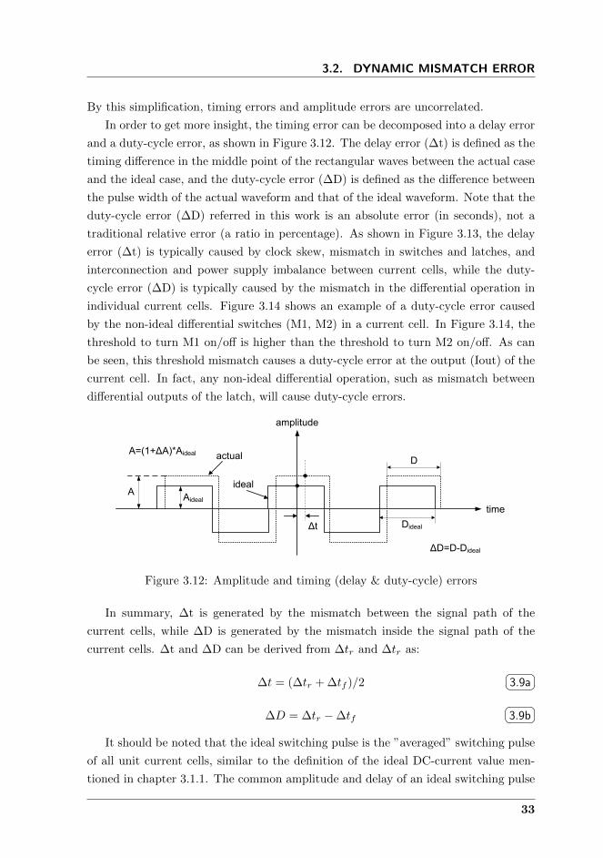
3.2. DYNAMIC MISMATCH ERROR
By this simplification, timing errors and amplitude errors are uncorrelated.
In order to get more insight, the timing error can be decomposed into a delay error
and a duty-cycle error, as shown in Figure 3.12. The delay error (∆t) is defined as the
timing difference in the middle point of the rectangular waves between the actual case
and the ideal case, and the duty-cycle error (∆D) is defined as the difference between
the pulse width of the actual waveform and that of the ideal waveform. Note that the
duty-cycle error (∆D) referred in this work is an absolute error (in seconds), not a
traditional relative error (a ratio in percentage). As shown in Figure 3.13, the delay
error (∆t) is typically caused by clock skew, mismatch in switches and latches, and
interconnection and power supply imbalance between current cells, while the duty-
cycle error (∆D) is typically caused by the mismatch in the differential operation in
individual current cells. Figure 3.14 shows an example of a duty-cycle error caused
by the non-ideal differential switches (M1, M2) in a current cell. In Figure 3.14, the
threshold to turn M1 on/off is higher than the threshold to turn M2 on/off. As can
be seen, this threshold mismatch causes a duty-cycle error at the output (Iout) of the
current cell. In fact, any non-ideal differential operation, such as mismatch between
differential outputs of the latch, will cause duty-cycle errors.
ΔD=D-Dideal
Dideal
ideal
Δt
time
Dactual
amplitude
A=(1+ΔA)*Aideal
AidealA
Figure 3.12: Amplitude and timing (delay & duty-cycle) errors
In summary, ∆t is generated by the mismatch between the signal path of the
current cells, while ∆D is generated by the mismatch inside the signal path of the
current cells. ∆t and ∆D can be derived from ∆tr and ∆tr as:
∆t = (∆tr + ∆tf )/2 3.9a
∆D = ∆tr −∆tf 3.9b
It should be noted that the ideal switching pulse is the ”averaged” switching pulse
of all unit current cells, similar to the definition of the ideal DC-current value men-
tioned in chapter 3.1.1. The common amplitude and delay of an ideal switching pulse
33

CHAPTER 3. MODELING AND ANALYSIS OF PERFORMANCELIMITATIONS IN CS-DACS
…...
decoder
clock
input data
D
Q
clk
current cell
Q
latch
D
Q
clk
current cell
Q
latch
D
Q
clk
current cell
Q
latch
Rload
clock skew
power supply
imbalance
switch mismatch interconnection
imbalance
latch mismatch
Figure 3.13: Error sources of the delay error
data+
data-
M1 M2data+ data-M1 threshold
Ioutcurrent cell
+ Iout -1 1
0
0 0
1
M2 threshold
ideal duty cycle
actual duty cycle
Figure 3.14: A duty-cycle error caused by a threshold mismatch between differentialswitches
only give a gain error and a latency of a DAC, but have no impact on the DAC’s
linearity, i.e. no impact on the DAC performance. However, an ideal pulse with non-
zero common duty-cycle error still contributes to non-linearities and decreases the
dynamic performance, such as SFDR, THD and IMD. This common duty-cycle error
is a non-mismatch global error and should be minimized by design as much as possi-
34

3.2. DYNAMIC MISMATCH ERROR
ble. How this common duty-cycle error affects the DAC’s dynamic performance will
be discussed in section 3.3.2. In this section, timing mismatch errors are assumed to
be Gaussian distributed with zero mean, i.e. the common duty-cycle error is assumed
zero.
Timing errors, including delay and duty-cycle errors, have no impact on the static
performance (DNL and INL). However, since timing errors are local errors and current-
cell dependent, timing errors will cause harmonic distortion and deteriorate the dy-
namic performance. Moreover, as will be explained in the next section, this effect will
become more dominant at high sampling frequencies.
Since RZ DACs typically have a re-sampling stage at the output, RZ DACs do not
suffer from timing mismatch errors, but still suffer from non-mismatch timing errors,
such as clock jitter and the common duty-cycle error. Those errors will be analyzed
for RZ DACs in section 3.3.
The effect of linearly distributed timing mismatch error on the dynamic perfor-
mance of NRZ DACs has been investigated in [41]. In the next section, the effect
caused by Gaussian distributed timing mismatch errors on the dynamic performance
of NRZ DACs will be analyzed.
3.2.1.2 Single-Tone SFDR/THD vs. Frequencies with Fixed Timing Er-
ror
Figure 3.15 shows the DAC outputs with and without timing errors, and the related
timing error pulses. Ts is the sampling period. As seen, the magnitude of the timing
Ts 2Ts 3Ts 4Ts 5Ts 6Ts
time
Δteq,nTs equivalent timing error per transition
without timing error
with timing error
y[nTs]
time
Figure 3.15: Timing error pulses
35

CHAPTER 3. MODELING AND ANALYSIS OF PERFORMANCELIMITATIONS IN CS-DACS
error pulse is determined by the step size (y) of the DAC output transition. y depends
on the difference between successive input digital codes (x):
y[nTs] = x[nTs]− x[(n− 1)Ts] 3.10
Equation 3.10 behaves as a first-order discrete-time differentiator. This digital differ-
entiator has a frequency magnitude response: |H(ω)digital| = 2sin(ω2 ) [42], as shown
in Figure 3.16. The frequency axis in that figure covers the positive frequency range
0 ≤ ω ≤ π samples/radian, corresponding to a cyclic frequency range of 0 to 0.5fs,
where fs is the sample rate in Hz [42]. For comparison reasons, the frequency mag-
nitude response of an ideal analog differentiator, |H(ω)analog| = ω, i.e. the derivative
of the input sine wave, is also shown in Figure 3.16. As seen, |H(ω)digital| matches
|H(ω)analog| accurately at very low frequencies. At high frequencies, |H(ω)digital| is
smaller than |H(ω)analog|. The relationship between |H(ω)digital| and |H(ω)analog| is:
|H(ω)digital| = |H(ω)analog| ×sin( fifsπ)
fifsπ
3.11
where fi is the input signal frequency. Then, for a sine wave input signal Asin(2πfit),
the magnitude of timing error pulses can be derived as:
y[nTs] =dAsin(2πfit)
dt|t=nTs
× Ts ×sin( fifsπ)
fifsπ
3.12
0 0.25π 0.5π 0.75π π (0.5fs)
0
0.25π
0.5π
0.75π
π
ω
|H(ω
)|
|H(ω)analog
|
|H(ω)digital
|
Figure 3.16: Frequency response of first-difference analog and digital differentiators
36

3.2. DYNAMIC MISMATCH ERROR
The duration of the timing error pulse at the sampling moment nTs is called
equivalent timing error per transition (∆teq,nTs). ∆teq,nTs
is calculated by averaging
the timing errors of all current cells that need to be switched at the sampling moment
nTs:
∆teq,nTs=
sum of the timing errors of the current cells that need to be switched
number of the current cells that need to be switched 3.13
Figure 3.17 shows ∆teq,nTsin a 14-bit 6T-8B segmented DAC (200 samples), with
the step size sweeping from one thermometer current cell to 63 thermometer current
cells. The timing error is assumed as Gaussian distributed with the standard deviation
σtiming=5ps for the 6-bit thermometer part (the 8-bit binary part has no timing
errors). As seen, due to averaging, ∆teq,nTsis decreasing with the number of current
cells that are switched together.
1 5 10 15 20 25 30 35 40 45 50 55 60 63−15
−10
−5
0
5
10
15
Step size [number of switched current cells]
equi
vale
nt ti
min
g er
ror
per
tran
sitio
n [p
s]
Figure 3.17: Equivalent timing error per transition ∆teq,nTs, 200 samples
Typically, ∆teq,nTsis within pico-second level and is far smaller than the sampling
period (Ts). For the DAC performance in the first Nyquist band, only the low fre-
quency components of timing error pulses are interesting. Therefore, to simplify the
analysis, the error pulse generated by the timing error can be approximated to a new
pulse which has a duration of one sampling period (Ts). As shown in Figure 3.18, the
equivalent amplitude error (∆Aeq,nTs) of the translated error pulse is calculated by
keeping the same charge as for the original timing error pulse. The reason to keep the
same charge/area is to let the original and the translated pulses have the same low
frequency components which are dominant in the performance. This simplification is
safe in most applications for the DAC performance in the first Nyquist band.
37

CHAPTER 3. MODELING AND ANALYSIS OF PERFORMANCELIMITATIONS IN CS-DACS
ΔAeq,nTstime
nTs (n+1)Ts
translation with same charge (area)
original timing error pulse
translated error pulse
Δteq, nTs
y[nTs]
Figure 3.18: Simplification of original timing error pulses
Therefore, for a Non-Return-to-Zero (NRZ) DAC with a sinusoid input signal
Asin(2πfinTs), the equivalent amplitude error (∆Aeq,nTs) can be calculated as:
∆Aeq,nTs= y[nTs]×
∆teq,nTsTs
=dAsin(2πfit)
dt|t=nTs
× Ts ×sin( fifsπ)
fifsπ
× ∆teq,nTsTs
= 2Aπficos(2πfinTs)×sin( fifsπ)
fifsπ
×∆teq,nTs 3.14
where fi is the frequency of the input sinusoidal signal, A is its peak amplitude, fs is
the sampling frequency.
Then, for a N-bit thermometer NRZ DAC, the total error power (Ptot,timing) gen-
erated by timing errors can be derived as:
Ptot,timing = (2πfiA√2
σtiming√πfi(2N−1)√
2fs
√√√√sin( fifsπ)fifsπ
)2 3.15
where σtiming is the standard deviation of Gaussian distributed timing errors in current
cells.
Since Ptot,timing is the total power generated by timing errors, it includes both the
linear error power Plinear,timing (located at the signal frequency) and the nonlinear
error power Pnonlinear,timing. Also due to the actual error distribution, there may also
be a part of error power located at DC (PDC,timing). To evaluate the DAC linearity,
only the nonlinear error power (Pnonlinear,timing) needs to be considered. Figure 3.19
compares the simulated Plinear,timing, Pnonlinear,timing and PDC,timing to Ptot,timing.
This Matlab simulation calculates the error power based on the original timing error
pulses shown in Figure 3.18, i.e. without simplification. As seen, when fi fs,
Pnonlinear,timing almost equals to Ptot,timing, and Plinear,timing is only a small part of
Ptot,timing. This is because when fi fs, due to the small step size, the equivalent
38

3.2. DYNAMIC MISMATCH ERROR
timing error per transition (∆teq,nTs) is highly random and largely spread as shown in
Figure 3.18, such that the timing error pulses are very little correlated to the signal.
As fifs
increases, due to the increased probability of large step size, ∆teq,nTsbecomes
smaller and the spread is less because of averaging, such that the timing error pulses
are more correlated to the signal. This results in a large portion of the total error
power being locating at the signal frequency. As seen in Figure 3.19, as fifs
increases,
the total error power (Ptot,timing) of timing errors pulses is more and more dominated
by the error power at the signal frequency (Plinear,timing). Plinear,timing is a linear
error and should not be counted as harmonic distortion. The error power at DC
(PDC,timing) should not be counted in the distortion neither. By fitting, the simulation
result in Figure 3.19 shows an empirical correlation factor between Pnonlinear,timing
and Ptot,timing as:
Pnonlinear,timing = (1− 0.83sin(fifsπ))Ptot,timing
3.16
10−2
10−1
100
0
0.5
1
1.5
2
2.5
3
3.5
4
4.5
5x 10
−20
Normalized input signal frequency fi/f
s
pow
er
Ptot,timing
, total power of timing error pulses
Plinear,timing
, error power at signal frequency
PDC,timing
, power at DC
Pnonlinear,timing
, total power of harmonics
Figure 3.19: Simulated power distribution of timing error pulses, mean value of 200samples
Then, the THD relative to the carrier, i.e. inverted signal-to-distortion ratio
(SDR), can be calculated as:
THDtiming =1
SDRtiming= (
PsigPnonlinear,timing
)−1 = (
A2
2 sinc2( fifsπ)
Pnonlinear,timing)−1
=4√
2πσ2timingfifs
(2N − 1)sinc( fifsπ)(1− 0.83sin(
fifsπ))
3.17
39

CHAPTER 3. MODELING AND ANALYSIS OF PERFORMANCELIMITATIONS IN CS-DACS
Note that since the duration of timing error pulses is very short compared to Ts, the
sinc-attenuation for the distortion generated by timing error pulses is very small in
the first Nyquist band. Therefore, as shown in Equation 3.17, no sinc-attenuation for
the distortion, only sinc-attenuation exists for the signal itself. This is different from
the case of amplitude errors, where both the signal and the distortion generated by
amplitude errors have sinc-attenuation.
The THD can also be expressed in dBc:
−THDtiming,dBc = SDRtiming,dBc
= 10log10(2N − 1)− 10log10(σ2timingfifs
1− 0.83sin( fifsπ)
sinc( fifsπ))− 12.5dBc 3.18
Monte-Carlo statistical simulations (200 samples) have been performed on a 14-
bit 6T-8B segment DAC to verify Equation 3.18. The Matlab simulation is based on
original timing error pulses without simplification. The standard deviation σtiming of
timing errors is assumed to be 5ps for the 6-bit thermometer part (the 8-bit binary
part has no timing errors). Figure 3.20(a) compares the THD results of Matlab
Monte-Carlo simulation and Equation 3.18 at 500MS/s. As shown, Equation 3.18
is well confirmed by the simulation result. Unlike amplitude errors whose effect on
the dynamic performance does not scale with frequencies, with given timing errors,
the effect of timing errors on the dynamic performance does scale with frequencies.
10−2
10−1
100
65
70
75
80
Normalized input signal frequency fi/f
s
−T
HD
[dB
c]
simulated, σtiming
=5ps, 500MS/s
calculated, σtiming
=5ps, 500MS/s
(a) Calculated and simulated THD
10−2
10−1
100
65
70
75
80
85
90
95
Normalized input signal frequency fi/f
s
SF
DR
[dB
]
simulated, σtiming
=5ps, 500MS/s
(b) Simulated SFDR
Figure 3.20: THD, SFDR vs. normalized input signal frequency at 500MS/s,σtiming=5ps. Bars: one sigma spread (200 samples)
40

3.2. DYNAMIC MISMATCH ERROR
As shown in Figure 3.20(a), for fi fs, -THD shows a 10dB/decade roll off with
fi at a fixed fs. The THD result for fi fs is similar to the result in [40] which
is based on a power spectral density calculation. Compared to [40], this work also
provided a simple equation for high fifs
. As seen, when fifs
is larger than 0.2, the curve
of -THD becomes flat with fi, which is due to the correlation between the errors and
the signal mentioned above. This conclusion also applies to the SFDR: as shown in
Figure 3.20(b), the simulated SFDR has a -15dB/decade roll-off with fi until fifs
=0.2,
then becomes flat. This phenomenon is also verified by the chip measurement results
in chapter 7.
The effect of timing errors at different sampling frequencies is easy to understand.
When keeping the same normalized input signal frequency fifs
, the proportion of tim-
ing errors per sampling period doubles for doubled fs. Therefore, the DAC’s dynamic
performance is expected to decrease 6dB in that case. In other words, the dynamic
performance should have a 20dB/decade roll-off with fs with the same normalized
input frequency. This also means that as the signal and sampling frequencies in-
crease, the effect of timing errors will dominate that of the amplitude errors. These
expectations are confirmed by Equation 3.18 and Matlab Monte-Carlo simulations at
different sampling frequencies (250MS/s, 500MS/s and 1GS/s) with σtiming=5ps, as
shown in Figure 3.21 and 3.22. In those figures, both the mean value and 3σ (99.7%)
yield curves of the SFDR and THD are shown. For example, in order to have at least
99.7% samples achieving >65dB SFDR across the whole Nyquist band at 250MS/s,
σtiming should be smaller than 5ps for this DAC example. Then, by keeping the ratio
10−2
10−1
100
60
65
70
75
80
85
250MS/s
500MS/s
1GS/s
Normalized input signal frequency fi/f
s
−T
HD
[dB
c]
simulatedcalculated
(a) Calculated and simulated THD mean value
10−2
10−1
100
50
55
60
65
70
75
80
85
Normalized input signal frequency fi/f
s
−T
HD
[dB
c]
250MS/s500MS/s1GS/s
(b) Simulated THD 3σ (99.7%) yield curves
Figure 3.21: THD vs. normalized input signal frequency at different sampling fre-quencies, σtiming=5ps (200 samples)
41

CHAPTER 3. MODELING AND ANALYSIS OF PERFORMANCELIMITATIONS IN CS-DACS
10−2
10−1
100
60
65
70
75
80
85
90
95
100
Normalized input signal frequency fi/f
s
SF
DR
[dB
]
250MS/s500MS/s1GS/s
(a) Simulated SFDR mean value
10−2
10−1
100
50
55
60
65
70
75
80
85
90
95
Normalized input signal frequency fi/f
sS
FD
R [d
B]
250MS/s500MS/s1GS/s
(b) Simulated SFDR 3σ (99.7%) yield curves
Figure 3.22: SFDR vs. normalized input signal frequency at different sampling fre-quencies, σtiming=5ps (200 samples)
of fifs
, every doubling of the sampling frequency will decrease the SFDR or THD by
6dB.
3.2.1.3 Single-Tone SFDR/THD vs. Timing Error with Fixed fs
It’s easy to understand that for a given sampling frequency (fs), signal frequency
(fi) and DAC architecture, larger timing errors cause larger harmonic distortion and
deteriorate the dynamic performance. The expected result is a 20dB/decade roll off
with the timing error for both the THD and SFDR.
Results of Equation 3.18 and Matlab Monte-Carlo simulations (200 samples) for
this 14-bit 6T-8B DAC are shown in Figure 3.23 and 3.24. Different Gaussian dis-
tributed timing errors are assumed for the 6-bit thermometer part with σtiming=2.5ps,
5ps and 10ps, respectively. The sampling frequency fs is 500MHz. It can be seen that
larger delay errors result in a worse dynamic performance: both SFDR and THD show
a 20dB/decade roll off with σtiming. The results are also in line with the analysis in
[40]. For example, as can be seen from the 3σ yield curves in Figure 3.24, in order to
have at least 99.7% samples achieving >65dB SFDR across the whole Nyquist band
at 500MS/s, σtiming should be smaller than 2.5ps. Then, every doubling of the timing
error will decrease the SFDR or THD by 6dB.
The dependence of the DAC performance on timing errors and frequencies are
summarized in Table 3.2 to give a clear overview.
42

3.2. DYNAMIC MISMATCH ERROR
Table 3.2: Summary of the effect of timing error on the performance of NRZ DACs
variables -THD or SFDR
timing error: σtiming -20dB/decade
frequencies: fs or fi-20dB/decade, when keeping the same fi
fs
for different fifs
, it depends on the actual situation as discussed
10−2
10−1
100
60
65
70
75
80
85
2.5ps
5ps
10ps
Normalized input signal frequency fi/f
s
−T
HD
[dB
c]
simulatedcalculated
(a) Calculated and simulated THD mean value
10−2
10−1
100
50
55
60
65
70
75
80
85
Normalized input signal frequency fi/f
s
−T
HD
[dB
c]
σtiming
=2.5ps
σtiming
=5ps
σtiming
=10ps
(b) Simulated THD 3σ (99.7%) yield curves
Figure 3.23: THD vs. normalized input signal frequency with different σtiming at500MS/s (200 samples)
10−2
10−1
100
60
65
70
75
80
85
90
95
100
Normalized input signal frequency fi/f
s
SF
DR
[dB
]
σtiming
=2.5ps
σtiming
=5ps
σtiming
=10ps
(a) Simulated SFDR mean value
10−2
10−1
100
50
55
60
65
70
75
80
85
90
95
Normalized input signal frequency fi/f
s
SF
DR
[dB
]
σtiming
=2.5ps
σtiming
=5ps
σtiming
=10ps
(b) Simulated SFDR 3σ (99.7%) yield curves
Figure 3.24: SFDR vs. normalized input signal frequency with different σtiming at500MS/s (200 samples)
43

CHAPTER 3. MODELING AND ANALYSIS OF PERFORMANCELIMITATIONS IN CS-DACS
3.2.2 Dynamic Mismatch in Frequency Domain
As we have seen, the dynamic mismatch is caused by both amplitude and timing
errors. It can be dominated by the amplitude error or the timing error, depending
on their values and the frequency. For low frequencies, the amplitude error is typi-
cally dominant in the dynamic mismatch, and the dynamic mismatch approaches the
static mismatch. With increasing sampling and signal frequencies, the timing error
becomes more and more visible. Consequently, for high-speed high-performance DAC
design, the dynamic mismatch has to be investigated and minimized, rather than just
minimizing the static mismatch.
The amplitude error can be measured by several methods, such as by means of
current comparators and ADCs [18, 30, 16, 15, 14, 25]. However, measuring a timing
error at pico-second level directly in the time domain is very difficult. In order to
evaluate both amplitude and timing errors, measuring the dynamic mismatch in the
frequency domain is an efficient way.
Instead of keeping the current cells at their static states to evaluate the static
matching in the time domain, in this analysis of the dynamic matching, the out-
puts of the current cells are modulated as rectangular waves. Figure 3.25 shows the
rectangular-wave output of an ideal unit current cell (without mismatch) and of the
i-th actual unit current cell (with mismatch), in both time and frequency domain.
Ai, Di are the amplitude and pulse width of the output of the i-th unit current cell,
respectively. ∆Ai, ∆Di, ∆ti are respectively the amplitude error (relative to the ideal
value), duty-cycle error and delay error of the i-th current cell, relative to the ideal
current cell. fm is the modulation frequency. As shown in Figure 3.25(b), because
of the property of the rectangular wave, the magnitude of frequency components are
shaped by a sinc function, where FUNDi, HC2i, HC3i, etc., are fundamental and
harmonic components of the modulated output of the i-th cell. FUNDideal, HC3ideal,
etc., are fundamental and odd harmonic components of the ideal current cell. For an
ideal current cell, due to its duty-cycle error is zero, the even harmonics of the ideal
cell are zero.
Then, dynamic-mismatch error Enfm (n=1, 2, 3, ...) is defined as the mismatch
error between an actual current cell and an ideal cell at the n-th order harmonic
frequency, e.g. Efm,i and E2fm,i are the mismatch errors in the fundamental com-
ponent FUNDi and the second harmonic component HC2i of the i-th current cell,
relative to an ideal cell, respectively. Since Enfm,i is a vector signal including both
magnitude and phase information, it can be shown in an I-Q vector plane. Figure
3.26 shows the mismatch error Enfm,i (n=1, 2, 3, 4) of the fundamental up to the
fourth harmonic components. How to measure the I-Q components will be given in
44

3.2. DYNAMIC MISMATCH ERROR
ΔDi=Di-Dideal
Dideal
ideal
Δti
time
Dii-th cell
Tm (=1/fm)
amplitude
(a) Time Domain
|HC2i|
fm 2fm 3fm 4fm
…...frequency
Mag
nitu
de
|FUNDi|
|FUNDideal|
(b) Frequency Domain
Ai=(1+ΔAi)*Aideal
AidealAi
|HC3i|
|HC3ideal| |HC4i|
Figure 3.25: Modulated rectangular output of current cells
chapter 5 and 6. Due to the property of the rectangular wave, for realistic mismatch
values, the mismatch error (Efm,i) at the fundamental frequency is dominated by the
amplitude error (∆A) and the delay error (∆t), and the mismatch error (E2fm,i) at
second harmonic is dominated by the amplitude error (∆A) and the duty-cycle error
(∆D). Therefore, the mismatch errors at the fundamental and the second harmonic,
i.e. Efm,i and E2fm,i, already include all mismatch information and can represent the
mismatch errors at all other harmonics. For instance, if Efm,i and E2fm,i are equal
to zero, mismatch errors at all other higher-order harmonics are also equal to zero.
Moreover, the mismatch errors at higher-order harmonic components are attenuated
by the sinc function such that those mismatch errors are negligible compared to Efm,i
and E2fm,i. Therefore, it is enough to just use Efm and E2fm to evaluate the dynamic
matching performance of current cells.
45

CHAPTER 3. MODELING AND ANALYSIS OF PERFORMANCELIMITATIONS IN CS-DACS
Efm,i
Ifm
Qfm
mismatch at fundamental, Efm,i=FUNDi-FUNDideal
FUNDideal
FUNDi
E2fm,i
I2fm
Q2fm
mismatch at 2nd harmonic, E2fm,i=HC2i due to HC2ideal=0
E3fm,i
I3fm
Q3fm
mismatch 3rd harmonic, E3m,i=HC3i-HC3ideal
E4fm,iI4fm
Q4fm
mismatch 4th harmonic, E4fm,i=HC4i due to HC4ideal=0
ideal
i-th current cell
HC3i
HC3ideal
Figure 3.26: Dynamic mismatch in I-Q plane (for clarity, axis are not to scale)
3.2.3 New Parameters to Evaluate Dynamic Matching: Dynamic-
DNL & Dynamic-INL
As described in chapter 2.2, the traditional DNL and INL are related to the differences
between the ideal and the measured static transfer functions and are the parameters
to evaluate the DAC’s static performance. An example of a static transfer function
is shown in Figure 3.27. Since the static transfer function is only determined by the
DC amplitude of the current cells, it is a one-dimensional curve with the digital input
codes.
However, since both amplitude and timing errors together contribute to the dy-
namic non-linearity, just DNL and INL are not enough to evaluate the matching per-
formance of current cells in current-steering DACs. Dynamic performance parameters,
such as the SFDR, THD and IMD, only give a consequence of mismatch errors, but
do not show the full relationship between the DAC’s dynamic linearity and mismatch
errors. In this section, two new parameters, called dynamic differential non-linearity
(dynamic-DNL) and dynamic integral non-linearity (dynamic-INL), are introduced to
46

3.2. DYNAMIC MISMATCH ERROR
000
001
010
011
100
101
110
111
amplitude of DAC output
static mismatch
Figure 3.27: One-dimensional static transfer curve of the static DAC output
evaluate the dynamic matching of current cells.
For the analysis of dynamic-INL and dynamic-DNL, a thermometer-coded DAC is
chosen as an example. Dynamic-INL and dynamic-DNL can be derived based on the
DAC’s dynamic transfer function. As the digital input code is increased from zero to
full scale, instead of measuring the static transfer function by sequentially turning on
unit current cells as DC-current outputs, for the dynamic transfer function analysis,
all unit current cells are sequentially turned-on and modulated as rectangular-wave
outputs at frequency fm. In other words: for the static transfer function, the DAC’s
output is a summed DC current of the current cells, while for the dynamic transfer
function, the DAC’s output is a sum of the modulated rectangular-wave output of
the current cells. Figure 3.28 shows an ideal and an actual dynamic transfer function
of the fundamental component of the modulated DAC output in an I-Q plane. As
shown, in the ideal case, with increasing input code, the fundamental component
(FUNDideal) of the DAC output linearly increases in magnitude, but keeps the same
phase. However, in the actual case, due to amplitude and timing mismatch errors,
the fundamental component (FUNDactual) has an non-linear increase in magnitude
47

CHAPTER 3. MODELING AND ANALYSIS OF PERFORMANCELIMITATIONS IN CS-DACS
Qfm
Ifm
Efm,001
Efm,010
Efm,011
Efm,100
Efm,101
Efm,110
transfer curve of fundactual,code
transfer curve of fundideal,code
000
001
010
011
100
101
110
111
Figure 3.28: Two-dimensional dynamic transfer curve of the fundamental componentof the modulated DAC output
and also has a varying phase. Compared to the one-dimensional static transfer curve
shown in Figure 3.27, the dynamic transfer function includes both magnitude and
phase information, and thus it is a two-dimensional curve with digital input codes. As
seen, Efm,code (code=0∼full scale digital input, i.e. 000, 001, ..., 111) is the integral
non-linearity error of the fundamental component at a given code input. Efm,code is
a sum of Efm of the current cells that are turned-on at that code input, given as:
Efm,code =FUNDactual,code − FUNDideal,code
=
code∑i=1
Efm,i, code=0∼full scale digital input
3.19
The same definition of E2fm,code and E3fm,code can be used for the integral non-
linearity errors of the second harmonic component (HC2) and the third harmonic
48

3.2. DYNAMIC MISMATCH ERROR
component (HC3), and so on. For example, E2fm,code can be derived as:
E2fm,code =HC2actual,code −HC2ideal,code
=
code∑i=1
E2fm,i, code=0∼full scale digital input
3.20
As mentioned in the previous section, Efm and E2fm already include all mismatch
information and they are the most dominant two errors. Therefore, the dynamic
integral non-linearity (dynamic-INL) in LSB can be defined as the RMS value of
the summed power of the integral dynamic mismatch of the fundamental and second
harmonic at every input code, i.e. summation of the power of Efm,code and E2fm,code,
over the power of the fundamental component of the modulated rectangular-wave
output of one ideal LSB cell:
dynamic-INLcode =
√|Efm,code|2 + |E2fm,code|2|FUNDideal,1LSB |2
LSB, code=0∼full scale 3.21
As seen, for optimization purposes, the dynamic-INL in Equation 3.21 is converted
back to a one-dimensional scalar with a unit of LSB, the same as the traditional static
INL. Similar to the INLmax, the dynamic-INLmax can be derived as:
dynamic-INLmax = max(dynamic-INLcode), code=0∼full scale 3.22
Similar to the DNL, the dynamic differential non-linearity (dynamic-DNL) is de-
fined as the RMS value of the power of the differential dynamic mismatch at every in-
put code, over the power of the fundamental component of the modulated rectangular-
wave output of one ideal LSB cell:
dynamic-DNLcode =
√(|FUNDcode|2 + |HC2code|2)− (|FUNDcode−1|2 + |HC2code−1|2)
|FUNDideal,1LSB |2− 1
, code=1∼full scale 3.23
Then, the dynamic-DNLmax can be derived as:
dynamic-DNLmax = max(dynamic-DNLcode), code=1∼full scale 3.24
3.2.4 Comparison to Traditional Static DNL & INL
Compared to the traditional DNL and INL that are used to evaluate the static match-
ing of current cells, the proposed dynamic-DNL and dynamic-INL include both ampli-
49

CHAPTER 3. MODELING AND ANALYSIS OF PERFORMANCELIMITATIONS IN CS-DACS
tude and timing mismatch errors to evaluate the dynamic matching of switched current
cells. Both the static and dynamic-switching behaviors of current cells are evaluated
by these two new parameters. By reducing the dynamic-DNL and dynamic-INL, both
amplitude and timing errors’ effect on the DAC’s static & dynamic performance will
be reduced. While by only reducing the traditional DNL and INL, the DAC’s static
performance is improved and the DAC’s dynamic performance is only partly improved
since the timing errors still exist. This advantage of the dynamic-DNL and dynamic-
INL over the traditional DNL and INL will be verified in chapter 5. In conclusion,
the dynamic-DNL and dynamic-INL describe the matching behavior of current cells
more completely and efficiently than the traditional DNL and INL.
By definition, the dynamic-DNL and dynamic-INL are parameters not only related
to amplitude and timing errors, but also modulation-frequency-dependent. Especially
when the modulation frequency fm is zero, the modulated rectangular-wave used to
measure the dynamic-DNL and dynamic-INL becomes a ’DC’ signal which is the
same situation when measuring the traditional DNL and INL. As a result, when fm is
zero, the dynamic-DNL and dynamic-INL are equal to the traditional DNL and INL,
respectively. Figure 3.29 shows an example of the dynamic-DNL and dynamic-INL
as fm increases. As can be seen, at fm = 0Hz, the dynamic-DNL and dynamic-INL
are equal to the traditional DNL and INL. This is obvious because at fm = 0Hz,
the dynamic-DNL and dynamic-INL are determined only by the amplitude error. As
fm increases, the timing error comes in, and becomes more and more dominant in
non-linearities.
traditional static DNL
dynamic-DNL
fm
contributed by timing errors
contributed by amplitude errors
0HZ (DC)
in L
SB
traditional static INL
dynamic-INL
fm
contributed by timing errors
contributed by amplitude errors
0HZ (DC)
in L
SB
Figure 3.29: dynamic-DNL, dynamic-INL vs. modulation frequency fm
In summary, if fm changes, the weight between the amplitude error and the timing
error in the dynamic mismatch changes, resulting in a frequency-dependent dynamic-
DNL and dynamic-INL. Actually, this opens a door to find an optimized weight func-
tion between amplitude and timing errors for different applications to achieve the best
performance. For example, more weight on the timing error for high sampling-rate
applications, and more weight on the amplitude error for low frequency applications.
50

3.3. NON-MISMATCH ERROR
How to improve the DAC’s performance based on the selection of fm and the opti-
mization of the dynamic-DNL and dynamic-INL will be discussed in chapter 5.
3.3 Non-Mismatch Error
3.3.1 Sampling Jitter
Sampling jitter of a Digital-to-Analog Converter (DAC) is considered as the uncer-
tainty in the updating time of the DAC output, as shown in Figure 3.30. As can
be seen, the jitter generates pulse-like errors in the DAC’s output. The jitter can
come from the device noise (thermal, 1/f), the power supply noise, interference cross-
modulation, etc. It may include jitter from the clock source (phase noise) and jitter
from the DAC itself. The jitter can be random or deterministic (such as sine or
square-wave modulated), dependent on the mechanism of the jitter generation. If the
sampling jitter is random and independent on the DAC’s input data , the effect of the
time
DAC output
jitter
error
time
nTs (n+1)Ts
Figure 3.30: Sampling Jitter
51

CHAPTER 3. MODELING AND ANALYSIS OF PERFORMANCELIMITATIONS IN CS-DACS
jitter behaves like white noise. In other words, the random sampling jitter does not
generate distortion, but only increases the noise floor and thus decreases the signal-to-
noise ratio (SNR). If the jitter is non-random and has a specific frequency component,
inter-modulation distortion will be generated.
As mentioned in chapter 2.1.1, ideal DACs do not generate quantization noise. In
order to show the jitter effect from the DAC itself, the quantization noise at the input
of the DAC is removed in the following analysis.
Since the jitter is also a kind of timing error, the translation of a timing error
to an equivalent amplitude error introduced in section 3.2.1.2 is used to convert the
jitter error pulse into an equivalent amplitude error. Assuming the jitter is Gaussian
randomly distributed, for a Return-to-Zero (RZ) DAC and a sine input signal, the
equivalent amplitude error (∆ARZ,nTs) of the translated jitter error pulse can be
calculated as:
∆ARZ,nTs = Asin(ωinTs)×∆tjitter,nTs
Ts
2
= Asin(2πfinTs)× 2∆tjitter,nTsfs
σ∆ARZ=
A√2× 2σjitterfs
3.25
where fi is the frequency of the input sinusoidal signal, A is its peak amplitude, fs is
the sampling frequency and σjitter is the variance of the jitter (rms value).
For a Non-Return-to-Zero (NRZ) DAC, the equivalent amplitude error (∆ANRZ,nTs)
of the translated jitter error pulse can be calculated as:
∆ANRZ,nTs =dAsin(2πfit)
dt|t=nTs
× Ts × sinc(fiπ
fs)× ∆tjitter,nTs
Ts
= 2Aπficos(2πfinTs)×∆tjitter,nTs × sinc(fiπ
fs)
σ∆ANRZ= 2
A√2πfi × σjitter × sinc(
fiπ
fs)
3.26
Then, the SNRs caused by the random jitter for a sinusoidal input signal in RZ
and NRZ DACs can be calculated as:
SNRjitter,RZ =Psig,RZPnoise,RZ
=
A2
2 sinc2( fiπ2fs
)× 12
( A√2
√2σjitter2fs)2 × 1
2
=sinc2( fiπ2fs
)
8σ2jitterf
2s
3.27a
SNRjitter,NRZ =Psig,NRZPnoise,NRZ
=
A2
2 sinc2( fiπfs )
(2πfiA√2σjittersinc(
fiπfs
))2=
1
4π2σ2jitterf
2i
3.27b
52

3.3. NON-MISMATCH ERROR
For RZ DACs, the same Gaussian distributed jitter is assumed for both rising and
falling edges. Due to the effect of return-to-zero, there are two jitter events in one
sampling period for RZ DACs, resulting in a total jitter spread of√
2σjitter, as shown
in Equation 3.27a.
The SNRs in decibels relative to the carrier for RZ and NRZ DACs can also be
derived as:
SNRjitter,RZ = −20log10(σjitterfs
sinc( fiπ2fs))− 9.03 dBc
3.28a
SNRjitter,NRZ = −20log10(σjitterfi)− 15.96 dBc 3.28b
Equations 3.28a and 3.28b are verified by Matlab Monte-Carlo statistical simula-
tions. The Matlab model calculates the SNR based on original jitter error pulses for
RZ and NRZ DACs. The Matlab simulation results (1000 runs) and Equations 3.28a,
3.28b are all plotted in Figure 3.31. The σjitter is 1ps and 2ps, respectively. The
sampling frequency is 100MHz and 200MHz, respectively. Since the jitter is common
for all current cells, the jitter effect is independent on the DAC’s architecture. As
shown, with Gaussian distributed random jitter, the theoretical model of Equation
3.28a and 3.28b accurately match the Matlab simulation results. Figure 3.31 also
shows that the translation error made during the translation from the jitter to the
equivalent amplitude error does not affect the accuracy. The same analysis method
can also be used for other types of jitter, such as sine-wave modulated jitter.
In summary, for RZ DACs:
• the SNR has a 20dB/decade roll-off with σjitter.
• the SNR has a 20dB/decade roll-off with the sampling frequency fs. When
fs doubles, due to double switching, the noise power spectrum density (NSD)
doubles. Together with the doubled noise bandwidth, it results totally in a
20dB/decade roll off in the SNR.
• the SNR is slightly affected by the sinc-attenuation, otherwise it is independent
of the signal frequency fi. Because of the return-to-zero effect, the NSD is only
dependent on the signal power, not the signal frequency. This is different from
the jitter effect of the ADC, where the SNR has a 20dB/decade roll-off with the
signal frequency and is independent of the sampling frequency.
For NRZ DACs:
• the SNR has a 20dB/decade roll-off with σjitter.
• the SNR is independent of the sampling frequency fs. When fs doubles, due to
53

CHAPTER 3. MODELING AND ANALYSIS OF PERFORMANCELIMITATIONS IN CS-DACS
0 10 20 30 40 5060
65
70
75
80
85
90
95
100
105
Input signal frequency [MHz]
SN
R [d
Bc]
RZ, simulatedRZ, calculatedNRZ, simulatedNRZ, calculated
2ps
1ps
2ps
1ps
(a) Calculated and simulated SNR at 100MS/s with different σjitter
0 0.1 0.2 0.3 0.4 0.560
65
70
75
80
85
90
95
100
105
Normalized input signal frequency
SN
R [d
Bc]
RZ, simulatedRZ, calculatedNRZ, simulatedNRZ, calculated
100MS/s
200MS/s
100MS/s
200MS/s
(b) Calculated and simulated SNR with σjitter=1ps for different fs
Figure 3.31: Jitter effect on the SNR of RZ and NRZ DACs
double switching and half transition step size, the NSD becomes half. Together
with the doubled noise bandwidth, it results in a constant SNR.
54

3.3. NON-MISMATCH ERROR
• the SNR has a 20dB/decade roll-off with the signal frequency fi. When fi dou-
bles, the transition step size of DAC’s output doubles, resulting in a quadruple
NSD.
• the SNR is much better than the SNR of RZ DAC at low normalized frequencies
(low fi/fs). This is because at low normalized frequencies, the amplitude of
the transition step in a NRZ DAC is much smaller than that in a RZ DAC.
Consequently, with the same jitter, the error in a NRZ DAC is also smaller than
that in a RZ DAC at low normalized input frequencies. As a result, for those
applications that have a critical noise requirement, a NRZ DAC will is a better
choice.
Table 3.3 gives a straight-forward summary of jitter effects in DACs, with the jitter
effect in ADCs as a reference.
Table 3.3: Summary of jitter effects on DACs and ADCs
variablesSNR of DAC
SNR of ADCRZ NRZ
σjitter -20dB/decade -20dB/decade -20dB/decade
fs -20dB/decade – –
fialmost constant, slightly
-20dB/decade -20dB/decadeaffected by sinc-attenuation
overall / ,performance
Compared to the jitter analysis of DACs in literature [43, 44, 45, 40], the proposed
analysis method is simple and straightforward, also with enough accuracy. References
[43, 45] assume that the jitter analysis method of ADCs is also valid for NRZ DACs,
but the proof is absent. In this work, based on a new and simple model, the analysis
for both RZ and NRZ DACs are performed that are easy to understand. Previous
research [44, 40] models the jitter effect based on a complicated PSD analysis of pulses,
which gives the same result for NRZ DACs, but 0.9dB difference for RZ DACs. This
0.9dB difference for RZ DACs may come from the fact that the same jitter is assumed
for both rising and falling edges in [44, 40] (i.e. the duration of a RZ pulse is fixed),
while a different jitter is assumed between rising and falling edges in this proposed
analysis (i.e. the duration of a RZ pulse is not fixed). In this work, a non-fixed
55

CHAPTER 3. MODELING AND ANALYSIS OF PERFORMANCELIMITATIONS IN CS-DACS
RZ pulse duration is used by assuming that the jitter in rising and falling edges are
uncorrelated.
3.3.2 Common Duty-Cycle Error
As mentioned in section 3.2.1.1, common amplitude, delay and duty-cycle errors in
current cells have different effects on the DAC’s performance:
• A common amplitude error gives a gain error of the DAC, but it has no impact
on the DAC’s performance.
• A common delay error gives an output latency of the DAC. This also has no
impact on the DAC’s performance.
• A common duty-cycle error is a global non-mismatch error and will decrease the
DAC’s dynamic performance. As mentioned in section 3.2.1.1, the duty-cycle
error is caused by non-ideal differential operations in current cells. As a result,
due to the common duty-cycle error, the DAC’s dynamic performance will be
suffer from a second harmonic distortion.
Figure 3.32 shows the common duty-cycle errors in thermometer-coded RZ and
NRZ DACs. As can be seen, for a sinusoidal input signal Asin(2πfit), the amplitudes
of the error pulses caused by the common duty-cycle error for RZ and NRZ DACs
follow the envelopes of |Asin(2πfit)| and |2πfiTsAcos(2πfit)sinc( fiπfs )|, respectively.
The Fourier series of f(t)=|Asin(2πfit)| is given by:
f(t) =A4
π(1
2− 1
3cos(2(2πfit))−
1
15cos(4(2πfit))−
1
36cos(6(2πfit))−
...− 1
(2n)2 − 1cos(2n(2πfit))), -π ≤ 2πfit ≤ π
3.29
Since the common duty-cycle error (Dcom) is a common error for all current cells,
similar to the jitter analysis in section 3.3.1, after converting the common duty-cycle
error into equivalent amplitude errors, the dominant second harmonic (HD2) relative
to the carrier, caused by the common duty-cycle error for RZ DACs can be calculated
according to Equation 3.29:
HD2com−duty,RZ = (Psig,RZPHD2,RZ
)−1 = (
A2
2 × sinc2( fiπ2fs
)× 12
( A√2
43π|Dcom|
2 × 2fs)2 × (2 + 2|cos(π 2fifs
)|)× 12
)−1
=16
9π2D2comf
2s (2 + 2|cos(π 2fi
fs)|) 1
sinc2( fiπ2fs) 3.30
56

3.3. NON-MISMATCH ERROR
time
DAC output
error
time(b) NRZ DAC
(a) RZ DAC
time
DAC output
error
time
Asin(2πfit)
|Asin(2πfit)|
Asin(2πfit)
|2πfiTsAcos(2πfit)sinc(πfi/fs)|
nTs (n+1)Ts
nTs (n+1)Ts
common duty-cycle error, 0.5Dcom
common duty-cycle error, 0.5Dcom
Figure 3.32: Common duty-cycle error
where Dcom is the common duty-cycle error in seconds, and fs, fi are the sampling
and input signal frequencies, respectively. According to the definition of the duty-
cycle error, timing errors in rising and falling edges are equal to half of the common
duty-cycle error (Dcom
2 ). Moreover, as shown in Figure 3.32(a), for RZ DACs, due to
the effect of return-to-zero, there are two identical error events in one sampling period.
These two error events have the same envelope, but with a input-frequency-dependent
phase shift. Thus, the total error power includes a correlation of (2 + 2|cos(π 2fifs
)|)for these two error events, as shown in Equation 3.30. This also means that the HD2
will reach its minimal value when the input signal frequency is around 0.25fs. This
expectation will be proven by later Matlab simulations.
57

CHAPTER 3. MODELING AND ANALYSIS OF PERFORMANCELIMITATIONS IN CS-DACS
For NRZ DACs, the HD2 can be derived as:
HD2com−duty,NRZ = (Psig,NRZPHD2,NRZ
)−1 = (
A2
2 sinc2( fiπfs )
(2πfiA√2
43π|Dcom|
2 sinc( fiπfs ))2)−1
=16
9D2comf
2i
3.31
With the common duty-cycle error, the SFDR is dominated by the HD2. Thus,
the SFDR for RZ and NRZ DACs, in decibel, can be derived as:
SFDRcom−duty,RZ = −HD2com−duty,RZ
= −10log10(D2comf
2s (2 + 2|cos(π 2fi
fs)|)
sinc2( fiπ2fs)
) + 7.44dB
3.32a
SFDRcom−duty,NRZ = −HD2com−duty,NRZ = −10log10(D2comf
2i )− 2.5dB
3.32b
Equations 3.32a and 3.32b have been verified by Matlab simulations, as shown in
Figures 3.33 and 3.34. The common duty-cycle error (Dcom) is set to 1ps, 2ps and
4ps, respectively. The sampling frequency is set to 200MHz, 400MHz and 800MHz,
respectively. As can be seen, the calculated theoretical model in Equations 3.32a
and 3.32b match Matlab simulation results very well. The Matlab model calculates
the SFDR/HD2 based on original error pulses caused by the common duty-cycle er-
ror, i.e. without converting the timing error into the equivalent amplitude error.
Thermometer-coded RZ and NRZ DACs are chosen as examples. Since the common
duty-cycle error is a common error existing in all current cells, the DAC architec-
ture, i.e. the number of thermometer bits, has no influence on the DAC performance.
The analysis results also apply to segmented DACs where the thermometer part is
dominant in the whole DAC performance.
As can be seen from Figure 3.33, the SFDR has a 20dB/decade roll-off with Dcom
for both RZ and NRZ DACs. Moreover, as expected in Equation 3.30, due to the
correlation of error signals, the RZ DAC achieves the best SFDR when the input
signal frequency (fi) is around 0.25fs. Compared to the SFDR when fi is at very low
or close to Nyquist rate, this best point of SFDR is 3dB better. For NRZ DACs, the
SFDR has a 20dB/decade roll-off with fi.
As shown in Figure 3.34 where fs is swept from 200MHz to 800MHz with normal-
ized input frequencies, the SFDR has a 20dB/decade roll-off with fs for RZ DACs and
is constant with fs for NRZ DACs at the same absolute input frequency, respectively.
The results are all in line with the derived theoretical Equations 3.32a and 3.32b.
The effects of the common duty-cycle error for RZ and NRZ DACs are summarized
58

3.3. NON-MISMATCH ERROR
0 0.1 0.2 0.3 0.4 0.560
65
70
75
80
85
Normalized input signal frequency [MHz]
SF
DR
or
−H
D2
[dB
c]
RZ: SimulationRZ: Calculation
1ps
2ps
4ps
0 0.1 0.2 0.3 0.4 0.565
70
75
80
85
90
95
100
105
Normalized input signal frequency [MHz]
SF
DR
or
−H
D2
[dB
c]
NRZ: SimulationNRZ: Calculation
1ps
2ps
4ps
Figure 3.33: SFDR/HD2 vs. input signal frequency with different common duty-cycleerrors at 200MS/s
59

CHAPTER 3. MODELING AND ANALYSIS OF PERFORMANCELIMITATIONS IN CS-DACS
0 0.1 0.2 0.3 0.4 0.560
65
70
75
80
85
Normalized input signal frequency [MHz]
SF
DR
or
−H
D2
[dB
c]
RZ: SimulationRZ: Calculation
200MS/s
400MS/s
800MS/s
0 0.1 0.2 0.3 0.4 0.565
70
75
80
85
90
95
100
105
Normalized input signal frequency [MHz]
SF
DR
or
−H
D2
[dB
c]
NRZ: CalculationNRZ: Simulation
200MS/s
400MS/s
800MS/s
Figure 3.34: SFDR/HD2 vs. normalized signal frequency with different samplingfrequencies, Dcom=1ps
60

3.3. NON-MISMATCH ERROR
in Table 3.4.
Table 3.4: Summary of the effect of the common duty-cycle error on the dynamicperformance
variablesSFDR or -HD2
RZ NRZ
common duty-cycle error: Dcom -20dB/decade -20dB/decade
fs -20dB/decade –
fiaffected by correlation and
-20dB/decadesinc-attenuation as discussed
architecture: thermometer-bit N – –
Overall Performance / ,
3.3.3 Finite Output Impedance
Another non-mismatch error that degrades the linearity of current-steering DACs is
the signal-dependent output impedance [46, 2]. As an example, a N-bit thermometer
DAC with M (=2N -1) current cells is shown in Figure 3.35. The number of current
cells on each side of the differential output depends on the input signal x (−1 ≤ x ≤ 1),
which equals (1+x)M2 and (1−x)M
2 respectively. Since the output impedance (Zo) of
L
(1+x)M/2
o
1
o
2
o
M
(1-x)M/2
Vout,diff
Figure 3.35: Input-signal dependent output impedance
61

CHAPTER 3. MODELING AND ANALYSIS OF PERFORMANCELIMITATIONS IN CS-DACS
a current cell is not infinite, the total output impedance is signal-dependent and
therefore the DAC’s linearity decreases.
Assuming that a non-linear system is described as y(t)= α1x+α2x2+α3x
3, the
third-order harmonic distortion (HD3) and the third-order intermodulation distortion
(IM3), which are most concerned in many communication systems, are given in [47]:
HD3 = 20log10(α3
4
α1 + α3
4
) ≈ 20log10(α3
4α1) dBc, for x = cos(ωt)
IM3 = 20log10(3α3
4 ( 12 )3
α1 + 9α3
4 ( 12 )2
) ≈ 20log10(3α3
32α1) dBc, for x =
1
2cos(ω1t)+
1
2cos(ω2t) 3.33
α1, α2, α3 are assumed independent on the input signal. Compared to the HD3 analysis
with a single input signal, half amplitude is assumed for both two input signals in the
IM3 analysis. This is also a typical case in the practical IM3 measurement. According
to Equation 3.33, for the same non-linear system, the IM3 is 8.52dB better than the
HD3.
The analysis of the non-linear behavior due to the finite output impedance was
introduced in [2]. The result of that analysis is given here as follows:
Vout,diff =RLIoM(1 + x)ZoRLM(1 + x) + 2Zo
− RLIoM(1− x)ZoRLM(1− x) + 2Zo
=RLMIo
2(
1 + x
1 + 2RLMZo
(1 + x)− 1− x
1 + 2RLMZo
(1− x))
3.34
Substituting a=RLM/2Zo, Vout,diff can be written as:
Vout,diff =RLMIo
2(
1 + x
1 + a(1 + x)+
x− 1
1 + a(1− x))
=RLMIoa2
(x
(1 + 1a )2 − x2
)
3.35
The Taylor expansion of equation 3.35 at x=0 is:
Vout,diff =RLIoM
(a+ 1)2(x+
x3
(1 + 1a )2
+ ...)
=RLIoM
(RLM2Zo
+ 1)2(x+
x3
(1 + 2Zo
RLM)2
+ ...)
3.36
62

3.3. NON-MISMATCH ERROR
Based on equation 3.33, the HD3 can be derived as:
HD3 = 20log10(α3
4
α1 + 3α3
4
) dBc ≈ 20log10(α3
4) dBc
= 20log10((1
2|1 + 2Zo
RLM|)2) dBc
3.37
If Zo is dominated by the output resistance (Ro) of the current cell at low frequen-
cies, the HD3 can be approximated as:
HD3Ro ≈ 20log10((1
2 + 4Ro
RL(2N−1)
)2) dBc 3.38
As shown in Equation 3.33, for the same non-linear system, the IM3 is 8.52dB better
than the HD3:
IM3Ro= 40log10(
1
2 + 4Ro
RL(2N−1)
)− 8.52 dBc 3.39
As seen, if Zo is dominated by the resistive part Ro, the effect of the finite output
impedance is independent of frequencies. In this case, the finite output impedance
is a kind of static error. Figure 3.36 shows the minimal Ro required for -90dBc IM3
performance with different thermometer bit N. RL is assumed to be 50ohm.
If Zo is dominated by 1/jωCo at high frequencies, where Co is the effective output
4 5 6 7 8 9 10 11 1210
4
105
106
107
N [bit]
requ
ired
Ro [o
hm]
RL=50 ohm
Figure 3.36: Minimal Ro required for -90dBc IM3 with different thermometer bit N
63

CHAPTER 3. MODELING AND ANALYSIS OF PERFORMANCELIMITATIONS IN CS-DACS
capacitance of the current cell defined in [2], the HD3 can be approximated as:
HD3Co≈ 20log10((
1
2| 2jωRLCoM
|)2) dBc = 40log10(
πfiRLCo(2N − 1)
2) dBc
3.40
And the corresponding IM3 can be expressed as:
IM3Co = 40log10(πfiRLCo(2
N − 1)
2)− 8.52 dBc
3.41
In the case of Zo dominated by the capacitive part at high frequencies, plots of the
relationship between the HD3/IM3 and the input signal frequency (fi) are shown in
Figure 3.37, where RL=50ohm, Co=6fF and N=6. As can be seen, the HD3 and IM3
have a 40dB/decade roll-off with fi. Therefore, for ultra high speed DACs, the finite
output impedance will significantly decrease the dynamic performance and limit the
SFDR/IMD. For example, depending on the process and circuit design, the output
impedance starts to limit the SFDR and IMD at a signal frequency of 180MHz in a
0.25µm CMOS DAC [15] or 400MHz in a 65nm CMOS DAC [2].
0 200 400 600 800 1000 1200 1400 1600 1800 2000
−130
−120
−110
−100
−90
−80
−70
−60
−50
−40
fi [MHz]
dBc
RL=50ohm, C
o=6fF, N=6
HD3IM3
Figure 3.37: HD3 and IM3 caused by finite output impedance versus fi
64

3.3. NON-MISMATCH ERROR
3.3.4 Data-Dependent Switching Interference
As shown in Figure 3.38, when switching a current cell, due to the parasitics and
non-ideal switches, switching interference is generated:
• Depending on the crossover point of the differential data inputs of the switches
(M1, M2), during the switching of the current from one side to another side,
M1 and M2 may both be switched off or on for a short time. This both-OFF
or both-ON states will cause a bounce in Vx at the common source node of M1
and M2. This voltage bounce will cause DAC non-linearities, e.g. the output
current of the current source (M0) will be modulated by this voltage bounce.
• Due to parasitics coupling and common biasing, voltage bounces in one current
cell might be coupled to other current cells. Then the output current of other
current cells will also be modulated by this coupled voltage interference. Fur-
thermore, the IR drops in the power supply network can also be affected by this
voltage interference, resulting in a switching-dependent power supply for each
current cell. Depending on the number of switching events at every sampling
point, the strength of this disturbance is different and input-data dependent.
biasing
Vx
data+
data-crossover point
bounce
M0
M1 M2data+ data-
Vx
Cparasitic
Both-OFF Both-ON
biasing
crossover point
bounce
current cell current cell current cell
…...
Figure 3.38: Switching Interference
65

CHAPTER 3. MODELING AND ANALYSIS OF PERFORMANCELIMITATIONS IN CS-DACS
As mentioned above, switching interference is related to the switching events and
are input-data dependent. Therefore, these data-dependent switching interference
will generate harmonic distortion and decrease the dynamic performance, such as the
SFDR and IMD. How severe this effect on the dynamic performance depends on the
topology of the current cells, biasing scheme and shielding techniques. Several design
techniques to reduce this effect will be discussed in chapter 4.
3.4 Summary of Performance Limitations
Based on the error properties, the non-idealities in CS-DACs are categorized into three
kinds of errors:
• Non-mismatch error: jitter, common duty-cycle error, finite output impedance,
data-dependent switching interference;
• Static-mismatch error: amplitude error;
• Dynamic-mismatch error: (amplitude + timing) errors.
As discussed, both non-mismatch and mismatch errors limit the static and dy-
namic performance of DACs. Random sampling jitter contributes to white noise,
which decreases the signal-to-noise ratio (SNR). In wireless communication applica-
tions where the requirement on noise performance is critical, a NRZ DAC is a better
choice than a RZ DAC. Unlike the common amplitude or timing error, the common
duty-cycle error is due to non-ideal differential operations and generates second har-
monic distortion. Therefore, the common duty-cycle error has to be minimized by
design as much as possible. Another non-mismatch error, finite output impedance,
can become a dominant error source at high signal frequencies, such as above 180MHz
in a 0.25µm CMOS DAC [15] or above 400MHz in a 65nm CMOS DAC [2], depending
on the process and circuit design.
For low to intermediate signal frequencies (from DC to around 400MHz), mismatch
errors are still the typical dominant error sources in recently reported state-of-the-
art CMOS DACs [2, 12, 10]. For near-DC signal frequencies, static errors, such as
amplitude errors, are dominant. The dynamic performance shows a 20dB/decade
roll-off with the amplitude error. In addition, the effect of the amplitude error does
not scale with frequencies: from a statistical point of view, the dynamic performance
(such as the SFDR, THD and IM3) is constant with sampling and signal frequencies.
However, the effect of the timing error does scale with frequencies: the dynamic
performance shows a 20dB/decade roll-off with the sampling frequency when keeping
the same normalized input signal frequencies. As a result, as signal and sampling
66

3.4. SUMMARY OF PERFORMANCE LIMITATIONS
frequencies increase, the timing error will become more important and the effect of
the timing error will exceed that of amplitude errors. Consequently, in order to achieve
both good static and dynamic performance, both amplitude and timing errors have to
be minimized. Figure 3.39 summaries how the DAC linearity, such as SFDR or IM3,
is typically affected by various error sources for different input signal frequencies.
1 10 100 1000
Linearity(SFDR, -IM3)
[dBc]
Input signal frequency [MHz]
static error dominatede.g. amplitude error,
output resistancetiming error dominated
output impedancedominated
-15dB/dec
-40dB/dec
0.2fs
Figure 3.39: Typical limitations on the DAC linearity by various error sources (fixedsampling frequency)
In this chapter, we simplified the mismatch errors of current cells into amplitude
and timing errors. Since the timing error can be decomposed into delay and duty-cycle
errors, it can be said that the dynamic mismatch is based on three-dimensional (3-
D) mismatch errors (amplitude, delay and duty-cycle errors), in contrast to that the
static mismatch is based on one-dimensional (1-D) mismatch error (amplitude error).
Actually, in more practical situations, due to the dynamic mismatch being measured
in the frequency domain, not only amplitude and timing errors, but all other kinds
of mismatch errors are also included in the final measured results. That is to say,
the dynamic mismatch and dynamic-DNL/dynamic-INL are based on all mismatch
errors, or in other words, based on any-dimensional (any-D) mismatch errors. Table
3.5 gives a summarized comparison between the concepts of the traditional static
mismatch and the proposed dynamic mismatch.
Moreover, as mentioned in section 3.2.4, dynamic-DNL and dynamic-INL are
frequency-dependent. This property of modulation-frequency dependency in the dynamic-
DNL and dynamic-INL gives an advantage of choosing a suitable weight function be-
tween amplitude and timing errors, so that the DAC’s performance can be optimized
for different applications. For example, more weight on the timing error for high fre-
quencies and vice versa. Based on the optimization of the dynamic matching, the
non-linearities caused by both amplitude and timing errors can be decreased. As a
67

CHAPTER 3. MODELING AND ANALYSIS OF PERFORMANCELIMITATIONS IN CS-DACS
Table 3.5: Comparison between static mismatch and dynamic mismatch
Static Mismatch Dynamic Mismatch
(Static Matching) (Dynamic Matching)
Purposeevaluate the static be-havior of current cells
evaluate the dynamic behaviorof current cells
Measured at DC@time domain fm & 2fm@frequency domain
Error covered 1-D: amplitude errorany-D: all mismatch errors,
or simplified 3-D: amplitude &timing (delay, duty-cycle) errors
Evaluationparameters
DNL, INL Dynamic-DNL, Dynamic-INL
result, both static and dynamic performance will be improved. Chapter 5 will intro-
duce a new design technique to improve the performance, based on the optimization
of the dynamic-INL.
3.5 Conclusions
In this chapter, the effect of various error sources on the DAC performance has been
analyzed. Theoretical equations have been developed to describe the relation between
these errors and the performance, and have been verified by Matlab simulations. The
outcome provides guidelines to find bottlenecks of the performance during designing
a high-performance CS-DAC.
Two novel design parameters, i.e. dynamic-DNL and dynamic-INL, have been
introduced to evaluate the matching of dynamic switching behavior between current
cells. The traditional static DNL and INL are only based on the amplitude error and
are used to only evaluate the DAC’s static performance. The proposed dynamic-DNL
and dynamic-INL are based on both amplitude and timing errors. Therefore, the
dynamic-DNL and dynamic-INL describe the matching between current cells more
completely and accurately.
Moreover, the frequency-dependent characteristic of dynamic-DNL and dynamic-
INL opens a door to choose a suitable weight function between amplitude and timing
errors, so that the DAC’s performance can be optimized for different applications. For
example, more weight on the timing error for high frequencies and vice versa. Based on
the optimization for the dynamic-DNL and dynamic-INL, the non-linearities caused
by both amplitude and timing errors can be decreased. As a result, both DAC static
and dynamic performance will be improved. A new design technique to improve the
68

3.5. CONCLUSIONS
performance, based on the optimization of the dynamic-INL, will be introduced in
chapter 5.
69


4Design Techniques for
High-Performance Intrinsic and Smart
CS-DACs
In the previous chapter, the non-idealities in CS-DACs have been discussed and their
impact on the DAC performance have been analyzed. In order to overcome these
performance limitations, emerging design techniques for high-performance intrinsic
and smart CS-DACs are introduced in this chapter. Firstly, the concept of smart
DACs is introduced as intrinsic DACs with additional intelligence to acquire and utilize
the actual chip information so that the performance/yield/reliability/flexibilty can be
improved. Then, existing design techniques for intrinsic and smart DACs are discussed
and summarized. Finally, a novel digital calibration technique for smart DACs, called
dynamic-mismatch mapping (DMM), is initially introduced in this chapter and will
be discussed further in the next chapters.
4.1 Introduction to Smart DACs
The smart concept implies on-chip intelligence to extract and use the actual chip in-
formation after manufacturing to improve the performance/yield/reliability/flexibility
beyond intrinsic limitations. As shown in Figure 4.1, a smart DAC includes two main
components:
• An intrinsic DAC.
71

CHAPTER 4. DESIGN TECHNIQUES FOR HIGH-PERFORMANCEINTRINSIC AND SMART CS-DACS
Actuator
Dig
ita
l p
re-p
roce
ssin
g
& d
eco
de
r
Current
Cells
Info.
Sensor
Intrinsic DAC
1 1 0 0
0 1 0 1
0 0 1 0
1 1 1 1
Smartness
analog domaindigital domain
Smart DAC
Processing
correction
Figure 4.1: Architecture of smart DACs
• A feedback loop with on-chip smartness, including information sensors, process-
ing circuits and actuators.
An intrinsic DAC is a basic DAC core designed based on a-priori knowledge. How-
ever, the actual chip information after manufacturing can not be accurately predicted
by a-priori knowledge. On-chip intelligence in a smart DAC enables to have the actual
chip information after chip production being fed back to the intrinsic DAC and utilize
this information. The actual information of each chip is measured by information
sensors. It might include error information, failure information, environment informa-
tion, input signal information, user information, etc. After some necessary processing,
actuators apply correction or optimization to the intrinsic DAC. This correction or
optimization involves:
• Calibration of actual errors of current cells, including mismatch and non-mismatch
errors, such that the DAC’s performance and yield are improved.
• Replacement of current cells that fail due to some reasons (such as design errors,
manufacturing failure, short life time, ESD breakdown, etc.) by redundant cells,
so that the whole chip can still be functional. This will increase the chip’s
performance, yield, reliability and life time.
Compared to calibrating the errors of current cells, replacing a failure cell is rather
easy. Therefore, this work focuses on the calibration and so on design techniques for
72

4.2. DESIGN TECHNIQUES FOR INTRINSIC DACS
high-performance DACs, i.e. design techniques that reduce the effect of non-idealities
on the performance.
In smart DACs, the feedback loop to improve the DAC’s performance is often
called a calibration loop which includes error measurement, error processing and error
correction. Since the DAC output is an analog signal, the error measurement has
to be done in analog domain. Depending on where and how the correction from the
actuator is applied, the calibration loop can be named as analog or digital calibration
techniques:
• Analog measurement, analog actuation → analog calibration techniques
• Analog measurement, digital actuation → digital calibration techniques
For example, if the errors are corrected in the digital domain, i.e. the correction is
done in digital pre-processing or decoding circuits, this calibration is called digital
calibration technique; if the errors are corrected in the analog domain, i.e. the cali-
bration is done in current cells, this calibration is called analog calibration technique.
The comparison between analog and digital calibration techniques will be given in
section 4.3.2.1.
The fundamental reason why a smart DAC can potentially achieve a better per-
formance than an intrinsic DAC is that a smart DAC measures, utilizes and calibrates
the actual information of every chip so that every chip can achieve its own optimized
performance. A smart DAC may retain this value for the rest of its useful life, or can
be reconfigured for a different environment or application. In other words, a smart
DAC provides an additional performance improvement or flexibility on an intrinsic
DAC. How much performance improvement can be obtained depends on how large
the errors in the intrinsic DAC are and how the on-chip smartness is implemented.
In the following sections, emerging design techniques for high-performance intrinsic
DACs and smart DACs are introduced. After the analysis of these existing techniques,
a novel calibration technique called dynamic-mismatch mapping (DMM), is introduced
for smart DACs in the first place and is compared to other techniques. In chapter 5,
the proposed DMM technique will be discussed in detail and the implementation will
be given in chapters 6 and 7.
4.2 Design Techniques for Intrinsic DACs
As discussed in Chapter 3, both non-mismatch and mismatch errors limit the per-
formance of intrinsic DACs. In order to overcome these problems, many design tech-
niques were proposed in recently published CS-DACs. Based on which error is focused
73

CHAPTER 4. DESIGN TECHNIQUES FOR HIGH-PERFORMANCEINTRINSIC AND SMART CS-DACS
on, these design techniques are divided into two groups: non-mismatch error related
techniques and mismatch error related techniques.
4.2.1 Non-Mismatch-Error Focused Techniques
As introduced in Chapter 3, non-mismatch errors mainly include sampling jitter, com-
mon duty-cycle error, finite output impedance and data-dependent switching interfer-
ence. In this section, design techniques to minimize the effects of these non-mismatch
errors in intrinsic DACs are discussed.
4.2.1.1 Sampling Jitter
As mentioned in Chapter 3.3.1, the sampling jitter in DACs has two sources:
• Jitter from clock sources, such as PLLs and oscillators.
• Jitter from the DAC itself.
Minimizing the jitter from clock sources requires low phase noise clock generators,
such as low phase noise PLLs and oscillators. Design of a low phase noise clock
generator is beyond the scope of this work which focuses on the DAC’s design.
Jitter from the DAC itself is mainly due to the noise in switches and power supplies
at the switching moment. In order to minimize the jitter effect due to the noise in
switches, the rule of thumb is to use the smallest transistor size in switches and large
drive current, so that the transition time of switching can be made as short as possible,
i.e. maximizing the dVdt . Multiple clocked-latch stages are also often used to make the
switching transitions as fast as possible in order to minimize the jitter generation, such
as two latch stages in [10] and three latch stages in [2]. An example of three clocked
latch stages is shown in Figure 4.2. As can be seen, with increasing drive ability
of latch stages, the transition time becomes shorter and shorter. Another benefit of
multiple latch stages is that the timing mismatch error is also reduced due to clock
re-sampling.
To minimize the jitter effect due to the noise from power supplies, the design of a
clean, low-impedance power supply network is very important. If the requirement of
the noise performance is highly concerned, it is recommended to use the current-mode
logic (CML) in critical signal paths. As shown in Figure 4.3, compared to CMOS logic,
CML logic has a constant, input signal independent current consumption, resulting in
a lower noise injection and less cross-talk to power supplies and the substrate [10].
74

4.2. DESIGN TECHNIQUES FOR INTRINSIC DACS
D Q
Clk
D Q
Clk
clock
input
latch stage 1 latch stage 2
transition time
to current cellD Q
Clk
latch stage 3
Figure 4.2: Multi-stage clocked-latches to minimize the jitter generation
CMOS logic CML logic
input-dependent current
constant current
Figure 4.3: CML logic vs. CMOS logic
4.2.1.2 Common Duty-Cycle Error
As mentioned in Chapter 3.3.2, the common duty-cycle error is due to non-ideal
differential operations in DACs. It generates second-order distortion and limits the
wide-band performance of the DAC. However, in some narrow-band applications where
the third-order intermodulation (IM3) is most important, such as multi-carrier OFDM
communication systems, the second-order intermodulation components (IM2) are out
of the signal band. Therefore, in those applications, the effect of the common duty-
cycle error is not of too much concern.
Current design techniques to minimize this common duty-cycle error in intrinsic
DACs still rely on the intrinsic matching of the transistors and the matching on the
layout. Measuring the common duty-cycle error is also difficult since it is at picosecond
75

CHAPTER 4. DESIGN TECHNIQUES FOR HIGH-PERFORMANCEINTRINSIC AND SMART CS-DACS
or even sub-picosecond level. Up to now, in any published DAC, there is no such a
technique or concept proposed yet to measure or calibrate this common duty-cycle
error.
4.2.1.3 Finite Output Impedance
Regarding the minimization of the impact of finite output impedance, simple cascoding
[10, 17, 15, 20] and always-on cascoding [48, 2] were developed.
As shown in Figure 4.4, simple cascoding is widely used to increase the output
impedance of current cells, especially at low signal frequencies where the output resis-
tance is dominant. As is well known, the output resistance is improved by gmro per
cascode stage.
Figure 4.4: Simple cascoding
However, at high signal frequencies, simple cascoding can not help too much. This
is because at high frequencies, the output capacitance (Co) is dominant in the output
impedance (Zo) of the current cells. A half-cell circuit of Figure 4.4 is shown in Figure
4.5. Depending on the ON or OFF state of the switch M2, the output impedance of
the current cell at high frequencies can be derived as [2]:
Zo,on ≈1
jωCo,on=
1
jω[(Cgd4 + Cp4 + (Cgs4+Cgd2+Cp2
gmro)on + (
Cgs2+Cgd1+Cp1
(gmro)2 )on + ...]
Zo,off ≈1
jωCo,off=
1
jω[(Cgd4 + Cp4 + (Cgs4+cgd2+Cp2
gmro)off ] 4.1
76

4.2. DESIGN TECHNIQUES FOR INTRINSIC DACS
M2 ON
M0
M1
M2
Co,on
Cgd4
Cgs4
Cp4
M4
Cgd2 Cp2
M2 OFF
Co,off
Cgd4
Cgs4
Cp4
M4
Cgd2 Cp2
Cgs2
Cp1
Figure 4.5: Half-cell circuit at M2 on/off state
where Cgd is the gate-drain capacitance, Cgs is the gate-source capacitance, and Cp is
the parasitic capacitance in the source and drain. For simplification, these capacitors
are assumed voltage-independent and all transistors are assumed to have the same
gain gmro.
As can be seen from Equation 4.1, since the ON or OFF state is decided by the
input signal, the difference (Co,diff ) between Co,on and Co,off results in a signal-
dependent output impedance:
Co,diff = Co,on − Co,off
= (Cgs4 + Cgd2 + Cp2
gmro)on − (
Cgs4 + Cgd2 + Cp2gmro
)off + (Cgs2 + Cgd1 + Cp1
(gmro)2)on + ... 4.2
where (Cgs4+Cgd2+Cp2
gmro)on - (
Cgs4+Cgd2+Cp2
gmro)off is typically the dominant part. For ex-
ample, if M4 is also totally turned off during the OFF state of M2, (Cgs4+Cgd2+Cp2
gmro)off
will be zero.
Adding another cascoding stage on top of M4 and M5 does not help because the
signal-dependent output impedance is always dominated by the output capacitance
of the most top cascode stage. In order to improve the output impedance at high
frequencies, a special cascoding called always-on cascoding was developed in [48, 2],
as shown in Figure 4.6. By always conducting a certain current in M4 and M5, i.e.
77

CHAPTER 4. DESIGN TECHNIQUES FOR HIGH-PERFORMANCEINTRINSIC AND SMART CS-DACS
current cell
always-on cascoding
M0
M1
M2 M3
M4 M5
Figure 4.6: Always-on cascoding
by making (Cgs4+Cgd2+Cp2
gmro)on more equal to (
Cgs4+Cgd2+Cp2
gmro)off , Co,diff can be sig-
nificantly reduced. Then, the output impedance becomes more independent of the
signal. Therefore, compared to simple cascoding, always-on cascoding can reduce the
distortion due to the signal-dependent output impedance also at high signal frequen-
cies.
4.2.1.4 Data-Dependent Switching Interference
As mentioned in Chapter 3.3.4, if the switching interference is data-dependent, it
will limit the DAC’s dynamic performance. For intrinsic DACs, in order to minimize
the effect of the switching interference generated during cell switching, a switching
scheme called constant switching is proposed to make the switching interference data-
independent [49, 12], as shown in Figure 4.7. The constant switching scheme guaran-
tees that there is always a switching action at every sampling clock in each current
cell, i.e. the current (Ics) interchanges its path between path A and path B at every
sampling clock. However, the output current (Io) of the current cell is still controlled
by the input data (D1 to D4) of the switches (M1 to M4), i.e. the sign of Io will
change or stay the same. By doing this, the switching interference is not input-data
dependent anymore, but becomes clock-frequency dependent. As shown in Figure
4.7, the distortion caused by the switching interference after constant switching will
appear at the clock frequency, which is unimportant for most applications.
Besides constant switching to shift the switching interference to the clock fre-
quency, another technique is also developed in [12] to really reduce the switching
interference by controlling the crossover point of input data signal to the switches.
78

4.2. DESIGN TECHNIQUES FOR INTRINSIC DACS
current cell with constant switching
M1 M2D1 M3 M4D2 D3 D4
Path A Path BIcs
+ Io -
0.5fclk fclk
fundamental
distortion
frequency
after constant switchng
fundamental image
Figure 4.7: Constant Switching Scheme
Since there is a feedback loop in this technique, it will be discussed in section 4.3.1.1,
as a design technique for smart DACs. Other basic design techniques to reduce switch-
ing interferences for intrinsic DACs include local biasing, low impedance power supply
and good layout shielding between current cells.
4.2.1.5 Design Techniques for Multiple Non-Mismatch Errors
Though the DAC’s non-linear behavior is caused by many error sources, if the DAC is
considered as a black box with certain non-linear behavior, techniques can be devel-
oped to minimize the whole non-linear behavior of the DAC. Harmonic suppression is
one of these techniques, as proposed in [50, 51].
The basic idea of harmonic suppression with a sine-wave input example is shown
in Figure 4.8. Assuming DAC1 and DAC2 have the same non-linear behavior, after
shifting the input signal of one DAC by 60, the third harmonic is shifted by 180
and will be canceled by that of the other DAC. However, in this harmonic suppres-
79

CHAPTER 4. DESIGN TECHNIQUES FOR HIGH-PERFORMANCEINTRINSIC AND SMART CS-DACS
sion technique, the same non-linear behavior is assumed for both DACs. That is to
say, harmonic suppression technique is particularly useful for global/systematic non-
mismatch errors [50, 51]. However, for random mismatch errors, two DACs do not
have the same non-linear behavior. Therefore, harmonic suppression technique with
a fixed 60 phase shift will not improve so much in that case, unless the non-linear
behavior of all sub-DACs is measured and certain algorithms are developed to cancel
the errors.
60o
DAC1
DAC2
180o
DAC1DAC2
fundamental component the 3rd harmonic
60oDAC2
DAC1
Asinωt summed output
Figure 4.8: Harmonic Suppression
4.2.2 Mismatch-Error Focused Techniques
To overcome the performance limitations caused by mismatch errors mentioned in
Chapter 3, minimizing mismatch errors in the design of intrinsic DACs is typically
based on following basic design rules:
• Properly size and bias the transistors in current sources to minimize the ampli-
tude error.
• Synchronize the data with the same clock and make the transition time of the
switching signal as short as possible to minimize the timing error.
• Make the layout as symmetrical as possible to minimize both amplitude and
timing errors.
The size of the transistors in current sources required for certain accuracy is already
discussed in Chapter 3.1.1. The required size depends on the quality of the process
80

4.2. DESIGN TECHNIQUES FOR INTRINSIC DACS
and the required accuracy. Besides sizing, the biasing for current sources is also very
important. Local biasing helps to reduce the biasing mismatch, as introduced in [40].
In order to minimize the timing error, strong drivers, multiple latch stages and the
symmetrical layout are often used in the clock and switching signal path [10, 2], as
shown in Figure 4.2.
Besides the basic rules, various advanced techniques were also proposed to improve
the performance of intrinsic DACs [32, 30, 31, 17, 19, 52, 40, 10, 41, 4, 23, 53], as
summarized in Table 4.1.
Table 4.1: Summary of advanced design techniques for intrinsic DACs
referencetargeted mismatch error
techniquesamplitude timing
[32, 30] common-centroid layout
[31] double common-centroid layout
[17] triple common-centroid layout
[19, 52] Q2 Random-Walk based switching se-quence
[40, 10] stochastic based switching sequence
[41] delay-difference cancelation basedswitching sequence
[4, 23, 53] dynamic element matching (DEM)
The layout techniques introduced in previous work [32, 30, 31, 17, 19, 52, 40, 10]
address amplitude errors caused by systematic process gradient errors. Those works
decompose each unit current source into several sub-elements and find an optimized
way to re-group these sub-elements into new unit current sources, so that the ampli-
tude mismatch error is reduced. The number of sub-elements is typically an integer
multiple of 2, such as 4 in [32, 31, 40] and even 32 in [30]. The more sub-elements, the
better error averaging, but more complex layout and larger chip area. Since the DAC’s
static linearity is determined by the accumulated amplitude errors, the switching se-
quence of current cells is also optimized to improve the INL caused by the systematic
amplitude error [19, 52, 40, 10] or to cancel the systematic delay errors [41]. How-
ever, those techniques are all based on the estimated systematic errors (i.e. process
spatial gradient errors) and can not reduce random amplitude or timing errors. Since
mismatch errors are random in a good design, most design techniques optimize those
81

CHAPTER 4. DESIGN TECHNIQUES FOR HIGH-PERFORMANCEINTRINSIC AND SMART CS-DACS
random errors based on on-chip error measurement. Those design techniques to re-
duce random amplitude and timing errors belong to the design techniques of Smart
DACs and will be discussed in the next section.
Beside layout techniques, another famous circuit design technique, called dynamic
element matching (DEM) or dynamic averaging, is proposed to optimize the effects
of both amplitude and timing errors [4, 23, 53]. DEM is widely used as a digital
performance-enhancement technique in many electronic designs, such as in ADCs,
DACs and sensors. The basic idea of DEM for DACs is randomizing the way of
using circuit elements, e.g. randomizing the switching sequence of current cells, so
that no signal-dependent errors are generated and the errors are averaged over time.
Therefore, with DEM, the error becomes a noise-like signal and no harmonic distortion
can be observed. However, due to randomization and distortion spreading, the noise
floor is significantly increased [12, 23], as shown in Figure 4.9. In short, DEM can only
improve the SFDR/IMD, but not the SNR/SNDR. For applications requiring critical
noise performance, such as in cellular base-stations, DEM is not suitable because of
its high noise floor.
0.5fclk
fundamental
distortion noise-like signalafter DEM
Figure 4.9: Spectrum spreading by DEM
4.3 Design Techniques for Smart DACs
Though lots of design techniques have been developed to improve the intrinsic DAC’s
performance, most of them can only deal with global non-mismatch errors and system-
atic mismatch errors, which is absolutely not enough to achieve excellent performance
after chip manufacturing, as because of process variations, the random mismatch er-
rors are quite different from die to die. Other design techniques for intrinsic DACs
that can deal with local random mismatch errors, such as DEM, which is blind to ac-
tual errors, can only decouple the distortion from the input signal so that no harmonic
distortion is generated, but at the cost of trading noise performance with harmonic
distortion performance as shown in Figure 4.9.
82

4.3. DESIGN TECHNIQUES FOR SMART DACS
As mentioned in section 4.1, this work targets on designing a high-performance
smart DAC, which is an intrinsic DAC with a calibration loop. By sensing and cor-
recting the actual error, calibration techniques can be developed to cover both global
non-mismatch and local mismatch errors, even together with the design techniques
for intrinsic DACs which are already discussed in section 4.2. Obviously, smart DACs
have a significantly strong potential to gain better performance than intrinsic DACs.
As also mentioned in section 4.1, depending on whether the error is corrected
in the analog domain or in the digital domain, the calibration techniques for smart
DACs are divided by analog calibration techniques and digital calibration techniques.
In the following, existing analog and digital calibration techniques are discussed and
compared. Based on the new concept of dynamic-INL introduced in section 3.2, a novel
digital calibration technique, called dynamic-mismatch mapping (DMM), is initially
proposed in this section, and will be discussed in detail in next chapters.
4.3.1 Analog Calibration Techniques
4.3.1.1 Techniques for Non-Mismatch Errors
Currently, for non-mismatch errors in DACs, such as sampling jitter, common duty-
cycle error and finite output impedance, no related calibration techniques were pub-
lished. To minimize the effect caused by these three non-mismatch errors, we still
have to rely on the design techniques for intrinsic DACs, as discussed in section 4.2.
To reduce the switching interference due to non-ideal cell switching which is de-
scribed in Chapter 3.3.4, an analog calibration technique is proposed in [12] to control
the crossover point of switching signals. As shown in Figure 4.10, by monitoring the
voltage bounce in Vx, the crossover point is controlled by a feedback loop, so that the
bounce in Vx and related interferences during switching can be minimized.
M0
M1 M2data+ data-
Vx
current cell
crossover
point control
Vrefdata+
data-
crossover point
Figure 4.10: Crossover-point control technique
83

CHAPTER 4. DESIGN TECHNIQUES FOR HIGH-PERFORMANCEINTRINSIC AND SMART CS-DACS
4.3.1.2 Techniques for Mismatch Errors
Most of the analog design techniques for smart DACs focus on calibrating current
sources, i.e. calibrating the amplitude error of current cells. Based on the litera-
ture investigation for published CMOS calibration DACs in recent 12 years, various
silicon-proven analog calibration techniques for amplitude errors were investigated,
as summarized in Table 4.2 [18, 30, 16, 15, 14, 25], with ascending order of their
publishing date (earliest on the top).
Table 4.2: Existing analog calibration techniques for amplitude errors
referenceexisting analog calibration techniques static
error sensing method calibration method performance
[18] ISSCC’00 Σ∆ ADC floating-gate trimming 0.5LSB@14b
[30] JSSC’03 current comparator floating-gate trimming 0.3LSB@14b
[16] ISSCC’03 off-chip 16b Σ∆ ADC CAL-DAC 0.5LSB@14b
[15] ISSCC’03 off-chip 6b SAR ADC CAL-DAC 0.65LSB@16b
[14] ISSCC’04 current comparator floating-gate trimming 0.65LSB@14b
[25] ESSCIRC’05 current comparator CAL-DAC 0.4LSB@12b
As can be seen from Table 4.2, for the static accuracy of 14-bit and above , calibrat-
ing the amplitude error is necessary. Using current comparators (can be considered
as 1-bit ADCs) and ADCs are two common methods to measure the amplitude error
directly in time domain. For calibrating the amplitude error, the biasing voltage of
the current source is trimmed using a floating-gate transistor [18, 30, 14] , as shown in
Figure 4.11(a). In [16, 15, 25], a small calibration current-steering DAC (CAL-DAC)
is used to calibrate the amplitude errors of current cells, as shown in Figure 4.11(b).
Regarding timing errors, up to this moment, no silicon-validated analog calibration
techniques are published for DACs. Only some concepts are proposed in [54, 55]. In
[54], by injecting a small current pulse, the glitch caused by the timing error can be
compensated. However, this technique is still in concept phase and the circuits of
measuring and calibrating the glitches are all missing, which could be a big challenge
in the circuit design.
In [55], timing errors in the rising and falling edges are separately measured by a
phase detector and are calibrated by tuning the substrate voltage of switch transistors
in latches. However, at this moment, no silicon was designed to prove this concept
yet.
84

4.3. DESIGN TECHNIQUES FOR SMART DACS
current cellcurrent cellcurrent cell
current cell
ADC
floating-gate trimming
current cellcurrent cellcurrent cell
current cell
ADCCAL-
DAC
feedback into current source
or feedback directly to DAC output
(a) floating-gate trimming
(b) CAL-DAC
Figure 4.11: Analog calibration techniques for the amplitude error
4.3.2 Digital Calibration Techniques
4.3.2.1 Digital vs. Analog Calibration Techniques
As shown in the previous section, although the error-sensing circuits can be turned off
when they are not used, analog calibration techniques still add additional active cir-
cuits into the DAC’s core in order to correct mismatch errors. Those additional active
circuits will create unwanted interference and add more parasitics. This is not desired
for high-speed DACs that require the high-speed analog part to be small/clean/less
parasitics as possible.
However, digital calibration techniques perform the correction in the digital do-
85

CHAPTER 4. DESIGN TECHNIQUES FOR HIGH-PERFORMANCEINTRINSIC AND SMART CS-DACS
main, such as in the digital pre-processing block or in the decoder, instead of in the
analog domain (i.e. in current cells). This is a big advantage of digital calibration
techniques over analog calibration techniques. This means less overhead, less para-
sitics & less interferences in the analog core of DACs, and more room for smartness.
As CMOS technology is continuously scaling down, digital circuits become more cost-
efficient and powerful. Therefore, this advantage will become more and more attractive
in the future. Moreover, digital calibration techniques are very easy to be ported to
another technology node.
The fundamental difference between digital and analog calibration techniques is
that digital calibration techniques improve the performance by reducing the effect of
the error, while analog calibration techniques improve the performance by reducing
the error itself. Although digital calibration techniques are quite different from analog
calibration techniques, in most cases, they do not conflict with each other. In general,
both digital and analog calibration techniques can be used together in one DAC. In
this situation, digital calibration techniques add additional performance improvement
on top of the performance achieved by analog calibration techniques.
In this section, existing digital calibration techniques for smart DACs are firstly
discussed. Based on the analysis of the deficiencies in existing techniques, a novel
digital calibration technique is proposed in this work to overcome the design chal-
lenges which are not covered by existing techniques. This new technique is initially
introduced in this section and will be discussed in detail in chapter 5.
4.3.2.2 Existing Digital Calibration Techniques: Mapping
If the nonlinear realtime transfer function of the DAC can be accurately measured and
modeled, the distortion can be digitally compensated by adding an inverse transfer
function as digital pre-processing before the DAC. However, measuring and model-
ing the nonlinear realtime transfer function of the DAC are very difficult, since the
transfer function is typically signal- and frequency- dependent. In practice, regarding
digital calibration techniques, currently only mapping techniques are developed and
implemented for the DAC design.
Mapping concepts have been extensively developed to minimize the mismatch error
in integrated circuits design. It defines a way of how to use existing circuit elements
optimally based on the measured information. For current-steering DACs, map-
ping means that the default switching sequence of the thermometer current
cells can be mapped to a new switching sequence, in order to optimize the
DAC performance. The mapping operation is typically combined with normal
binary-to-thermometer decoding operation. Since mapping techniques are based on
86

4.3. DESIGN TECHNIQUES FOR SMART DACS
the measured mismatch errors, the optimized switching sequence is different from sam-
ple to sample. Thus, a large freedom in mapping is required. The freedom of mapping
depends on how the mapping decoder is implemented. For full mapping freedom, a
reconfigurable memory is often used as a mapping decoder [35, 56, 57]. Since mapping
is done in the decoder, it is fully digital. Therefore, it has all advantages belonging to
digital calibration techniques.
According to how many kinds of errors are covered, mapping techniques can be
categorized into one-dimensional and multi-dimensional mapping techniques. As the
name suggests, one-dimensional mapping techniques only calibrate one specific kind of
errors, while multi-dimensional mapping techniques calibrate multiple kinds of errors
simultaneously. Obviously, multi-dimensional mapping techniques are more attractive
and can have better performance than one-dimensional mapping techniques.
I. One-Dimensional Mapping
Similar to the situation of analog calibration techniques for smart DACs, all published
one-dimensional mapping techniques with validated-silicon only focus on calibrating
amplitude errors [35, 56, 51, 58], i.e. the main target is to improve the static perfor-
mance (INL, DNL). Since amplitude errors are static errors, those mapping techniques
belongs to static-mismatch mapping (SMM). Figure 4.12 shows an example of static-
mismatch mapping. As can be seen, after mapping, the INL is improved since the
integral amplitude error is reduced. Table 4.3 summarizes existing static-mismatch
mapping techniques for smart DACs. In [35, 56, 58], by measuring amplitude errors,
the switching sequence of the thermometer current cells is optimized to reduce the
INL based on amplitude-error cancelation. While in [51], benefit from parallel sub-
optimized switching sequencedefault switching sequence
1 2
3 4 5
67
2
345
67
1
INL
code
INLmax
INL
code
INLmax
Figure 4.12: Example of static-mismatch mapping (SMM)
87

CHAPTER 4. DESIGN TECHNIQUES FOR HIGH-PERFORMANCEINTRINSIC AND SMART CS-DACS
DACs, similar to changing the switching sequence, the codes distributed to sub-DACs
can be optimized to reduce both DNL and INL. As also shown, with static-mismatch
mapping, the INL reduction factor is typically around 2, i.e. 1-bit improvement on
the static linearity. Since the timing error is not covered by static-mismatch map-
ping (SMM), the improvement by SMM on the DAC’s dynamic performance is only
observed at very low frequencies and is negligible at high frequencies [58, 51].
Table 4.3: Summary of existing static-mismatch mapping techniques (SMM)
referenceexisting digital calibration techniques INL reduction
error measurement correction method factor
[35] JSSC’88 current comparatorSMM (change switch-ing sequence)
1.36
[56] TSCASI’05 VCOSMM (change switch-ing sequence)
1.78
[51] current comparatorSMM (change codedistribution)
1.5
[58] JSSC’07 current comparatorSMM (change switch-ing sequence)
2.2
Several concepts of one-dimensional mapping for timing errors have been pro-
posed in [59, 60, 38]. Similar to static-mismatch mapping, mapping for timing errors
optimizes the switching sequence by sorting timing errors such that the dynamic per-
formance can be improved. As mentioned before, the DAC’s dynamic performance
is affected by both amplitude and timing errors. Just mapping for amplitude errors
or just mapping for timing errors is not enough to guarantee a good performance at
high frequencies. Therefore, multi-dimensional mapping techniques are required to
calibrate both amplitude and timing errors at the same time.
II. Multi-Dimensional Mapping
A concept for multi-dimensional mapping using cost function for the combination
of amplitude and timing errors was firstly introduced in [61]. This concept requires
both amplitude and timing errors to be separately measured. However, due to the
limitation of the circuit implementation, it is very difficult to measure timing errors
in sub-picosecond accuracy. In this work, a new method is proposed that combines
amplitude and timing errors as vector errors in the frequency domain. Then, based
on the measured vector errors, a novel multi-dimensional mapping technique called
dynamic-mismatch mapping is introduced and validated with silicon results.
88

4.3. DESIGN TECHNIQUES FOR SMART DACS
4.3.2.3 A Novel Multi-Dimensional Mapping Technique: Dynamic-Mis-
match Mapping
Though digital calibration techniques have lots of potential advantages as described
previously in section 4.3.2.1, currently existing digital calibration techniques, such
as static-mismatch mapping, are only based on the static mismatch error (i.e. the
amplitude error of current cells) and their main achievement is the improvement on
the DAC’s static performance (e.g. the INL). However, as explained in chapter 3.2,
the dominant source of mismatch errors in high-speed high-performance CS-DACs
is the dynamic mismatch between current cells, not the static mismatch. This is
because with increasing sampling frequency, the timing error becomes more and more
important and dominant [15, 12, 10, 2], as proven in chapter 3.2.1.2 and 3.2.1.3.
Therefore, in order to achieve high dynamic performance for DACs with high sampling
rates, the dynamic mismatch that includes both amplitude and timing errors has to
be optimized, instead of just optimizing the static mismatch.
In this work, a novel digital calibration technique called dynamic-mismatch
mapping (DMM) is introduced that is validated with experimental results in chap-
ter 7. As a multi-dimensional mapping technique, dynamic-mismatch mapping cal-
ibrates both amplitude and timing mismatch errors. It optimizes the switching se-
quence of thermometer current cells based on reducing the dynamic-INL (a parameter
introduced in chapter 3.2.3 based on combining amplitude and timing errors as vec-
tor errors), instead of reducing the static-INL in traditional static-mismatch mapping
techniques. Thus, not only the DAC static performance, but also the dynamic per-
formance can be improved. The details of dynamic-mismatch mapping technique will
be given in chapter 5. A dynamic-mismatch sensor based on a Zero-IF receiver has
also been developed to measure the dynamic mismatch errors, as will be described in
chapter 6.
Since dynamic element matching (DEM) is also a digital performance-enhancement
technique which can cover both amplitude and timing errors, it is necessary to compare
dynamic-mismatch mapping (DMM) with DEM. Table 4.4 compares the proposed
DMM calibration technique with existing digital calibration techniques, i.e. traditional
static-mismatch mapping (SMM) and DEM. This work is the first reported DAC that
measures both amplitude and timing mismatch errors, and corrects them in the digital
domain. Moreover, due to the mismatch effect being reduced instead of randomized
by DEM, the proposed DMM will not increase the noise floor. As will be verified by
the experimental results of the proposed DMM DAC in chapter 7, the proposed DMM
DAC provides a comparable harmonic-distortion performance to the state-of-the-art
DEM DACs [4, 23, 53], and a much better noise performance than those DEM DACs.
89

CHAPTER 4. DESIGN TECHNIQUES FOR HIGH-PERFORMANCEINTRINSIC AND SMART CS-DACS
Table 4.4: Comparison of digital calibration techniques for mismatch errors
reference techniquestargeted mismatch errors
noise figureamplitude error timing error
[35, 56, 57, 51] SMM # ,[4, 23, 53] DEM G# G# /this work DMM ,
# Only for systematic errors.G# For both systematic and random errors, but these errors are not being measured.And noise performance is sacrificed. Both systematic and random errors are measured.
What has to be emphasized is that because mapping techniques improve the DAC’s
performance by only changing the switching sequence, the room of performance im-
provement in every chip sample depends on how good the default switching sequence
is and how the mismatch error distributes. It’s strongly recommended to design an
intrinsic DAC as good as possible and have the mismatch errors linearly or Gaussian
distributed, so that the errors can be easily canceled and mapping techniques can
provide maximum benefits. In other words, mapping techniques are more suitable to
achieve additional performance improvement on the top of an intrinsic DAC. If only
relying on the design techniques for intrinsic DACs and analog calibration techniques
for smart DACs, the improvement on the performance will become more and more
difficult, or become less efficient. For example, in order to improve the performance
of the state-of-the-art DACs, every extra bit in static accuracy or every additional
6dB in the SFDR/IMD will significantly increase the complexity and cost in analog
design. In that case, as mentioned in section 4.3.2.1, digital calibration techniques,
such as mapping techniques, can overcome this bottleneck and further improve the
DAC’s performance to the next level.
4.4 Summary of Design Techniques for Intrinsic and Smart
DACs
In order to overcome the design challenges analyzed in Chapter 3, emerging silicon-
proven design techniques for high-performance intrinsic and smart CS-DACs have been
introduced in this chapter, as summarized in Table 4.5. In Table 4.5, digital techniques
for the DAC’s performance enhancement are marked with gray background color.
90

4.4. SUMMARY OF DESIGN TECHNIQUES FOR INTRINSIC AND SMARTDACS
Tab
le4.
5:S
um
mar
yof
emer
gin
gd
esig
nte
chn
iqu
esfo
rh
igh-p
erfo
rman
cein
trin
sic
an
dsm
art
DA
Cs
tech
niq
ue
refe
ren
ceN
on
-mis
matc
hE
rror
Mis
matc
hE
rror
ou
tpu
tim
p.
SW
IA
mp
litu
de
Tim
ing
IntrinsicDACs
alw
ays-
onca
scod
ing
[48,
2]
√
con
stan
tsw
itch
ing
[49,
12]
√
har
mon
icsu
pp
ress
ion
[50,
51]
√√
CS
layo
ut
tech
niq
ues
[32,
30,
31,
17,
19,
52,
40]
#
del
ayca
nce
lati
on[4
1]
#
dyn
amic
elem
ent
mat
chin
g(D
EM
)[4
,23,
53]
G#G#
SmartDACs
cros
sover
contr
ol[1
2]
√
CS
floa
tin
g-ga
tetr
imm
ing
[18,
30,
14]
CA
L-D
AC
[16,
15,
25]
stat
ic-m
ism
atch
map
pin
g(S
MM
)[3
5,56,
57,
51]
dyn
amic
-mis
mat
chm
app
ing
(DM
M)
this
work
#O
nly
for
syst
emati
cer
rors
.G#
For
bot
hsy
stem
atic
and
ran
dom
erro
rs,
bu
tth
ese
are
not
bei
ng
mea
sure
d.
An
dn
ois
ep
erfo
rmance
issa
crifi
ced
.
Bot
hsy
stem
atic
an
dra
nd
om
erro
rsare
mea
sure
d.
91

CHAPTER 4. DESIGN TECHNIQUES FOR HIGH-PERFORMANCEINTRINSIC AND SMART CS-DACS
For non-mismatch errors like sampling jitter and common duty-cycle error, cur-
rently we still rely on a good clock generator and intrinsic transistor/layout match-
ing. For non-mismatch errors like finite output impedance and switching interference
(SWI), always-on cascoding, constant switching, harmonic suppression and crossover
control techniques are proposed to overcome these challenges, as discussed in section
4.2.1 and 4.3.1.1.
For mismatch errors, most design techniques for intrinsic DACs, such as layout
techniques for current sources and delay cancelation technique in [32, 30, 31, 17, 19,
52, 40, 10, 41, 4, 23, 53], can only deal with systematic amplitude or timing errors.
Dynamic element matching (DEM) can reduce the harmonic distortion caused by
both systematic and random amplitude or timing errors, however, at the cost of a
significantly increased noise floor.
In order to further reduce mismatch errors, analog and digital calibration tech-
niques have been developed for smart DACs to measure and calibrate the actual mis-
match errors. Analog calibration techniques, such as floating-gate trimming in current
sources and current compensation by using a lite calibration-DAC (CAL-DAC), are
widely used in the published state-of-the-art DACs. Compared to analog calibration
techniques, digital calibration techniques, such as traditional static-mismatch map-
ping (SMM) and the proposed dynamic-mismatch mapping (DMM), have less active
circuits, less interference and less parasitics in the analog core of the DAC. Especially
when pushing the DAC to extremely high performance, for analog calibration tech-
niques, to increase one extra bit in the static accuracy or 6dB in the SFDR/IMD/THD,
will require substantial design effort including dedicated analog circuits and resources
of power and area. In this case, due to the errors being corrected in the digital domain,
digital calibration techniques will have less challenges and will be more efficient than
analog calibration techniques.
Currently existing digital calibration techniques, i.e. static-mismatch mapping
techniques (SMM) [35, 56, 57, 51], are only based on the amplitude error of current
cells. As a result, the main benefit from those SMM techniques is the improvement on
the DAC’s static performance, such as the INL. However, the benefit on the DAC’s
dynamic performance is quite limited to low signal and sampling frequencies, because
for high signal and sampling frequencies, the effects of timing errors becomes more and
more visible. Therefore, in order to not only improve the DAC’s static performance,
but also improve the DAC’s dynamic performance within the whole Nyquist band,
both amplitude and timing mismatch errors have to be taken into account, especially
for high sampling frequencies.
Dynamic-INL is a new parameter introduced in chapter 3 to evaluate the dynamic
mismatch between current cells, which covers both amplitude and timing mismatch
92

4.5. CONCLUSIONS
errors. In contrast to static-mismatch mapping that optimizes the traditional static
INL which is only based on amplitude errors of current cells, in this work, a novel
digital calibration technique, called dynamic-mismatch mapping (DMM), is in-
troduced to optimize the dynamic-INL so that both the DAC’s static and dynamic
performance can be improved. This technique will be discussed in detail in chapter 5.
Compared to DEM, as will be verified by experimental results of the proposed
DMM DAC in chapter 7, the proposed DMM DAC can provide a comparable harmonic-
distortion performance to the state-of-the-art DEM DACs [4, 23, 53], and a much
better noise performance than those DEM DACs.
4.5 Conclusions
In this chapter, design techniques for high-performance current-steering DACs have
been discussed. For classifying these design techniques, the concept of smart DACs
is introduced. A smart DAC is an intrinsic DAC with additional on-chip intelligence
to enhance the performance/yield/reliability/flexibility. It always includes a feedback
loop which is typically composed of information sensing circuits, processing circuits
and actuators. Based on the measured actual chip information, every chip sample
can achieve its best performance/reliability/life time. This big potential advantage
of smart DACs over intrinsic DACs makes the development of design techniques for
smart DACs highly necessary.
Based on where and how the errors are corrected, design techniques for smart
DACs can be categorized by analog and digital calibration techniques. Comparison
of analog and digital calibration techniques are given showing that digital calibration
techniques have less overhead and less parasitics in the analog core of DACs. For
a high speed design, a clean and small DAC core is preferred, which makes digital
calibration techniques very attractive. Furthermore, in most cases, digital calibration
techniques can be stacked on top of analog calibration techniques to achieve additional
performance benefits.
Current digital calibration techniques for smart DACs only address on amplitude
errors. As signal and sampling frequencies increasing, the effect of timing errors
becomes more dominant than that of amplitude errors. In order to reduce the effect
of both amplitude and timing errors, a novel digital calibration technique, called
dynamic-mismatch mapping (DMM), is initially proposed In this chapter and will
be discussed in detail in the next chapter. Compared to traditional static-mismatch
mapping (SMM), DMM can improve the performance across the whole Nyquist band,
especially at high frequencies. This advantage of DMM over SMM is due to both
amplitude and timing errors being corrected. Compared to dynamic element matching
93

CHAPTER 4. DESIGN TECHNIQUES FOR HIGH-PERFORMANCEINTRINSIC AND SMART CS-DACS
(DEM), DMM does not increase the noise floor because the mismatch effect is reduced
instead of randomized.
94

5A Novel Digital Calibration Technique:
Dynamic-Mismatch Mapping (DMM)
In this chapter, a novel digital calibration technique, called dynamic-mismatch map-
ping (DMM), is proposed to correct the non-linear effect caused by both amplitude
and timing mismatch errors. The theoretical background of this proposed DMM is
firstly explained. How to implement DMM in an easy and efficient way is discussed
next. Matlab Monte-Carlo statistical simulations are also performed in this section
to show the performance improvement by DMM, with a comparison to traditional
static-mismatch mapping techniques. Finally, the application of DMM is discussed
and summarized.
5.1 Theory of Dynamic-Mismatch Mapping
As introduced in chapter 4.3.2.2, mapping techniques for DACs are digital calibration
techniques to optimize the switching sequence of current cells such that the DAC’s
performance can be improved. Figure 5.1 shows the Matlab simulation results of
SFDR and THD of a 14-bit, 6Thermometer-8Binary (6T-8B) segmented DAC with
five randomly chosen switching sequences of thermometer current cells (MSBs). As
can be seen, with fixed amplitude and timing errors, the use of different switching
sequences for MSBs in a very wide spread of performance. This implies that by just
digitally optimizing the switching sequence of thermometer current cells (i.e. map the
default switching sequence to an optimized switching sequence in the digital domain),
95

CHAPTER 5. A NOVEL DIGITAL CALIBRATION TECHNIQUE:DYNAMIC-MISMATCH MAPPING (DMM)
0 0.05 0.1 0.15 0.2 0.25 0.3 0.35 0.4 0.45 0.550
55
60
65
70
75
14−bit, 6T−8B segmented DAC @fs=1GHz
Normalized input signal frequency
SF
DR
[dB
c]
0 0.05 0.1 0.15 0.2 0.25 0.3 0.35 0.4 0.45 0.5
−70
−65
−60
−55
−50
14−bit, 6T−8B segmented DAC @fs=1GHz
Normalized input signal frequency
TH
D [d
Bc]
Figure 5.1: SFDR and THD with five randomly chosen switching sequences of MSBsfor the same DAC
both performance and yield can be significantly improved.
Existing static-mismatch mapping (SMM) techniques optimize the switching se-
quence only based on amplitude errors of current cells. However, in most applications,
current cells are used as switched current cells, rather than static current sources.
As defined in chapter 3.2, dynamic mismatch is the mismatch between the dynamic
switching behavior of current cells, including both amplitude and timing errors. An
example of the dynamic-mismatch error in the differential output of the i-th current
cell, in time, frequency and I-Q domain, are given in Figure 5.2. Obviously, as con-
cluded in chapter 3.2.4, compared to static mismatch, dynamic mismatch represents
the matching of switched current cells more completely and accurately. Similar to
that the INL and DNL are developed to evaluate the static-matching between current
cells, in chapter 3.2, dynamic-INL and dynamic-DNL are also introduced to evaluate
the dynamic-matching between current cells.
96

5.1. THEORY OF DYNAMIC-MISMATCH MAPPING
dynamic mismatch
timing error at rising edges
amplitude error (static mismatch)
timing error atfalling edges
(a) dynamic mismatch in time domain
(c) dynamic mismatch in a I-Q plane
i-th cell
ideal cell
time
Mag
nitu
de
|HC2i|
fm 2fm 3fm 4fm
…...frequency
|FUNDi|
|FUNDideal|
(b) dynamic mismatch in frequency domain
Efm,i=FUNDi-FUNDideal
Ifm
Qfm
mismatch at fundamental
FUNDideal
FUNDi
I2fm
Q2fm
mismatch at second harmonic
E2fm,i=HC2i, due to HC2ideal=0
Figure 5.2: Dynamic mismatch in time, frequency and I-Q domain
Instead of the traditional static-mismatch mapping optimizing the switching se-
quence and improving the DAC’s performance by reducing the integral static-mismatch
error (i.e. the INL) based on only amplitude errors [35, 56, 57, 51], the proposed
dynamic-mismatch mapping (DMM) technique improves the DAC’s performance by
reducing the integral dynamic-mismatch error (i.e. the dynamic-INL) so that the
error effect of both amplitude and timing errors can be reduced. The advantage of
dynamic-mismatch mapping over static-mismatch mapping is that dynamic-mismatch
mapping can improve the DAC’s dynamic performance even at high frequencies, where
a significantly less improvement can often be seen in static-mismatch mapping in
[35, 56, 57, 51]. This advantage will be verified by Monte-Carlo statistical analysis in
97

CHAPTER 5. A NOVEL DIGITAL CALIBRATION TECHNIQUE:DYNAMIC-MISMATCH MAPPING (DMM)
section 5.3 and silicon measurement results in chapter 7.
As defined in chapter 3.2.3, the dynamic-INL is given as:
dynamic-INLcode =
√|Efm,code|2 + |E2fm,code|2|FUNDideal,LSB |2
=
√|∑codei Efm,i|2 + |
∑codei E2fm,i|2
|FUNDideal,1LSB |2LSB, code=0∼full scale 5.1
The proposed dynamic-mismatch mapping (DMM) reduces the dynamic-INL ac-
cording to certain criteria. A simple criterion is used in this work as an example:
DMM changes the switching sequence of thermometer current cells, such
that the dynamic-mismatch error of each cell can be maximally canceled
by that of the following cell. More complex mapping criteria may reduce the
dynamic-INL even more. However, this simple sorting criterion combines an easy
implementation in hardware with also rather good performance.
Clearly, if we want to find two current cells whose dynamic-mismatch errors can
cancel each other, since dynamic-mismatch errors are vector signals, they should be
canceled in the I-Q plane. As shown in Figure 5.3, the (i+1)-th current cell following
the i-th current cell in the switching sequence is found by minimizing the summed
dynamic-mismatch error of these two cells, i.e. find a cell from unsorted cells such
that
|Efm,i + Efm,i+1|2 + |E2fm,i + E2fm,i+1|2
= (Ifm,i + Ifm,i+1)2 + (Qfm,i +Qfm,i+1)2 + (I2fm,i + I2fm,i+1)2 + (Q2fm,i +Q2fm,i+1)2 5.2
is minimal; the (i+2)-th, (i+3)-th current cells in the switching sequence and so on
are found one-by-one from the unsorted current cells by the same principle. The
room for optimization reduces during mapping since the number of the unsorted cells
become less and less. Therefore, the current cell with largest dynamic-mismatch error
is compensated at the first place. By sorting all current cells in this way, the dynamic-
INL can be reduced.
In summary, the proposed dynamic-mismatch mapping technique finds the opti-
mized switching sequence based on the relative position between dynamic-mismatch
errors of all current cells in the I-Q plane. The absolute values of the dynamic-
mismatch errors have no effect on finding an optimal switching sequence. Only the
relative position between the dynamic-mismatch errors of all current cells in the I-Q
plane is the deterministic factor in this digital mismatch-calibration technique. How
98

5.2. MEASUREMENT OF DYNAMIC-MISMATCH ERROR
fm,i
fm
fm
2fm,i
2fm
2fm
fm,i+1 2fm,i+1
……
cancelation cancelation
Figure 5.3: Dynamic-Mismatch Mapping
much the dynamic-INL can be reduced and how much the DAC’s static & dynamic
performance can be improved by DMM will be discussed in section 5.3.
5.2 Measurement of Dynamic-Mismatch Error
5.2.1 Measurement Flow
In order to optimize the switching sequence with dynamic-mismatch mapping, the
dynamic-mismatch errors of all current cells have to be accurately measured. As
proposed in chapter 3.2.2, in contrast to static mismatch that can be easily measured in
the time domain [18, 30, 16, 15, 14, 25], dynamic mismatch can be efficiently measured
in the frequency domain by modulating current cells as rectangular-wave outputs.
According to the definition of the dynamic-INL in Equation 5.1, only the dynamic-
mismatch errors at the fundamental and second harmonic (Efm and E2fm) need to
be measured. Since Efm and E2fm are vector signals, both I and Q components of
Efm and E2fm have to be measured. The easiest way to measure the I/Q component
of a vector signal is using an I/Q mixer to convert both components of the signal to
DC and then measure them. Based on this idea, a dynamic-mismatch error sensor
based on a zero-IF receiver is developed in this work. The block architecture of this
dynamic-mismatch sensor is shown in Figure 5.4(a), and the circuit implementation
will be given in chapter 6. Since an ideal current cell does not exist, the current cells
are firstly measured relative to a reference cell (an arbitrary-chosen cell) as E′
nfm,
then the actual dynamic-mismatch errors Enfm of current cells can be achieved by
subtracting the averaged errors. As shown, the output of the i-th current cell and of
the reference current cell are modulated with opposite phases as rectangular waves,
99

CHAPTER 5. A NOVEL DIGITAL CALIBRATION TECHNIQUE:DYNAMIC-MISMATCH MAPPING (DMM)
so that the ac signal at the summation node only comprises the dynamic-mismatch
error (E′
i,nfm). Then, the mismatch signal is demodulated by a sine LO and down-
converted to DC by a I/Q mixer. After converting E′
i,nfm to Ei,nfm by subtracting
the averaged error, the I-Q components, such as Ifm,i and Qfm,i for Efm, will be
digitized by ADCs. The LO can be chosen at fm or 2fm to measure Efm or E2fm.
LO at fm or 2fm
cellref
celli
square wave at fm -
+
I'fm,i or I'2fm,i
outputref(t)
outputi(t)
e'i(t)
90°
LOsin,I(t)
LOsin,Q(t)
E'fm,i
FUNDi
FUNDref
I'fm,i
Q'fm,i
demodulated mismatch at fundamental, relative to the reference cell
ΔDi=Di-Dref
DrefΔti
time
Di
Tm (=1/fm)
Ai=(1+ΔAi)*Aideal
ArefAi
outputi(t)outputref(t)
averaging
+-
I'fm or I'2fm
Ifm,i or I2fm,i
Q'fm,i or Q'2fm,i
averaging
+ -
Q'fm or Q'2fm
Qfm,i or Q2fm,i
Qfm
Ifm
Efm,i
Qfm
Ifm
Qfm,i=Q'fm,i-Q'fm,i
Ifm,i=I'fm,i-I'fm,i
demodulated mismatch at fundamental, relative to the ideal cell
(a) Measurement flow of dynamic-mismatch error, sine-wave LO
(b) Modulated output of i-th and reference cells in time domain
(c) Demodulated mismatch at fundamental in a I-Q plane
ADC
ADC
Figure 5.4: I/Q demodulation by a sine-wave LO
100

5.2. MEASUREMENT OF DYNAMIC-MISMATCH ERROR
As shown in Figure 5.4(b), the amplitude of the i-th current cell (celli) and of the
reference cell (cellref ) are Ai and Aref , respectively. The duty-cycle of celli and of
cellref are Di and Dref , respectively (note that in this work, the duty-cycle is defined
as the absolute duration of the pulse width, not a ratio in percentage). The delay
error of celli, relative to cellref , is ∆ti. The modulation frequency and period are
fm and Tm, respectively. Then, the modulated rectangular-wave outputs of celli and
cellref can be expressed as:
outputref (t) =4ArefDref
Tm
∞∑n=1
sin2πnfmDref
22πnfmDref
2
sin(2πnfmt)
outputi(t) =4AiDi
Tm
∞∑n=1
sin 2πnfmDi
22πnfmDi
2
sin(2πnfmt+ n∆tiTm
2π)
5.3
Next, the dynamic-mismatch error e′
i(t) of celli, relative to cellref , can be derived
as:
e′
i(t) = outputi(t)− outputref (t) =
∞∑n=1
e′
nfm,i(t) 5.4
Since the LO is a sine-wave signal, only the mismatch-error at the fundamental
frequency, i.e. e′
fm,i, is converted to DC. e′
fm,i can be derived from e′
i as:
e′
fm,i(t) =4AiDi
Tm
sin 2πfmDi
22πfmDi
2
sin(2πfmt+∆tiTm
2π)− 4ArefDref
Tm
sin2πfmDref
22πfmDref
2
sin(2πfmt)
=4Aisin(πfmDi)
πsin(2πfmt+
∆tiTm
2π)− 4Arefsin(πfmDref )
πsin(2πfmt) 5.5
With reasonable mismatch value and modulation frequency, sin(πfmDi) ≈ 1,
hence e′
fm,i can be simplified as:
e′
fm,i(t) ≈4Aiπsin(2πfmt+
∆tiTm
2π)− 4Arefπ
sin(2πfmt) 5.6
Then, the I-Q components (I′
fm,i, Q′
fm,i) of the demodulated fundamental mis-
101

CHAPTER 5. A NOVEL DIGITAL CALIBRATION TECHNIQUE:DYNAMIC-MISMATCH MAPPING (DMM)
match error (E′
fm,i) of celli, relative to cellref , can be calculated as:
I demodulation: e′
fm,i(t)× LOsine,I(t) = e′
fm,i(t)×ALO,sinsin(2πfmt− φLO)
≈ −2ALO,sinAiπ
[cos(2π2fmt+∆tiTm
2π − φLO)− cos(∆tiTm
2π + φLO)]+
2ALO,sinArefπ
[cos(2π2fmt− φLO)− cos(φLO)]
⇒ I′
fm,i ≈2ALO,sin
π[Aicos(
∆tiTm
2π + φLO)−Arefcos(φLO)]
Q demodulation: e′
fm,i(t)× LOsine,Q(t) = e′
fm,i(t)×ALO,sincos(2πfmt− φLO)
≈ 2ALO,sinAiπ
[sin(2π2fmt+∆tiTm
2π − φLO) + sin(∆tiTm
2π + φLO)]−
2ALO,sinArefπ
[sin(2π2fmt− φLO) + sin(φLO)]
⇒ Q′
fm,i ≈2ALO,sin
π[Aisin(
∆tiTm
2π + φLO)−Arefsin(φLO)] 5.7
where φLO is the phase difference between LO and the reference cell.
Finally, as shown in Figure 5.4(c), the actual mismatch error (Efm,i) of celli
relative to the ideal cell can be derived by subtracting the averaged errors:
Ifm,i = I′
fm,i −1
N
N∑n=1
I′
fm,i
Qfm,i = Q′
fm,i −1
N
N∑n=1
Q′
fm,i, N=number of cells
5.8
The measured Efm,i with I-Q components (Ifm,i, Qfm,i) in Equation 5.8 can be
used in dynamic-mismatch mapping to optimize the switching sequence. The same
calculation can be applied when measuring E2fm,i.
However, for practical circuit design, a square-wave LO is much easier to be gen-
erated than a sine-wave LO. With a square-wave LO, dynamic-mismatch errors at all
other odd harmonics (e.g. E′
3fm,i, E′
5fm,i, etc.) will fold into DC together with the
error (E′
fm,i) at the fundamental. As will shown in the next section, this does not
change the relative positions between the dynamic-mismatch errors of the current cells
and will not affect the mapping performance. Figure 5.5 shows the measurement flow
102

5.2. MEASUREMENT OF DYNAMIC-MISMATCH ERROR
LO at fm or 2fm
cellref
celli
square wave at fm -
+
I'odd,i or I'even,i
outputref(t)
outputi(t)
e'i(t)
90°
LOsquare,I(t)
LOsquare,Q(t)
averaging
+ -
I'odd or I'even
Iodd,i or Ieven,i
Q'odd,i or Q'even,i
averaging
+ -
Q'odd or Q'even
Qodd,i or Qeven,i
(a) Measurement flow of dynamic-mismatch error, square-wave LO
(b) Demodulated mismatch at odd harmonics in a I-Q plane
ADC
ADC
Eodd,i
Qodd
Iodd
Qodd,i=Q'odd,i-Q'odd,i
Iodd,i=I'odd,i-I'odd,i
E'odd,iODDi
ODDref
I'odd,i
Q'odd,i
demodulated mismatch at odd harmonics, relative to the reference cell
Qodd
Iodd
demodulated mismatch at odd harmonics, relative to the ideal cell
Figure 5.5: I/Q demodulation by a square-wave LO
with a square-wave LO demodulation. The square-wave LO is given as:
LOsquare,I(t) =4ALOπ
∞∑n=1
1
2n− 1sin[2π(2n− 1)fmt− (2n− 1)φLO]
LOsquare,Q(t) =4ALOπ
∞∑n=1
1
2n− 1cos[2π(2n− 1)fmt− (2n− 1)φLO]
5.9
where ALO is the peak amplitude of square wave and φLO is the phase difference
between LO and the reference cell.
Then, the I-Q components (I′
odd,i, Q′
odd,i) of demodulated odd harmonics mismatch
103

CHAPTER 5. A NOVEL DIGITAL CALIBRATION TECHNIQUE:DYNAMIC-MISMATCH MAPPING (DMM)
error (E′
odd,i), demodulated by the square-wave LO, can be derived as:
I demodulation: e′
odd,i(t)× LOsquare,I(t) =
∞∑n=1
e′
(2n−1)fm,i× LOsquare,I(t)
⇒ I′
odd,i ≈8ALOπ2
(
∞∑n=1
Ai(2n− 1)2
cos[(2n− 1)(∆tiTm
2π + φLO)]−
∞∑n=1
Aref(2n− 1)2
cos[(2n− 1)φLO])
Q demodulation: e′
odd,i × LOsquare,Q(t) =
∞∑n=1
e′
(2n−1)fm,i× LOsquare,Q(t)
⇒ Q′
odd,i ≈8ALOπ2
(
∞∑n=1
Ai(2n− 1)2
sin[(2n− 1)(∆tiTm
2π + φLO)]−
∞∑n=1
Aref(2n− 1)2
sin[(2n− 1)φLO])
5.10
According to the theory of Fourier series,∑∞n=1
1(2n−1)2 cos[(2n− 1)x] = π
4 (π2 − x)
for 0 ≤ x ≤ π. Hence, Iodd,i and Qodd,i can be rewritten as:
I′
odd,i ≈
2ALO
π Ai[π2 − (∆tiTm
2π + φLO)]−Aref (π2 − φLO) if 0 ≤ φLO ≤ π2ALO
π −Ai[ 3π2 − (∆ti
Tm2π + φLO)] +Aref ( 3π
2 − φLO) if π ≤ φLO ≤ 2π
Q′
odd,i ≈
2ALO
π Ai[π − (∆tiTm
2π + φLO)]−Aref (π − φLO) if −π2 ≤ φLO ≤π2
2ALO
π −Ai[2π − (∆tiTm
2π + φLO)] +Aref (2π − φLO) if π2 ≤ φLO ≤
3π2 5.11
Finally, as shown in Figure 5.5(b), the actual mismatch error (Eodd,i) of celli
relative to the ideal cell, demodulated by the square-wave LO at frequency fm, can
be derived by subtracting the averaged errors:
Iodd,i = I′
odd,i −1
N
N∑n=1
I′
odd,i, and Qodd,i = Q′
odd,i −1
N
N∑n=1
Q′
odd,i
5.12
where N is number of measured current cells. The same calculation can be applied
when measuring the I-Q components (Ieven,i, Qeven,i) of Eeven,i with a square-wave LO
at 2fm frequency. With square-wave demodulation, the dynamic-mismatch mapping
will use Eodd,i and Eeven,i to optimize the switching sequence, instead of Efm,i and
E2fm,i. As will shown in the next section, the same switching sequence will be found
by dynamic-mismatch mapping, no matter if it is a sine-demodulation or square-
demodulation.
104

5.2. MEASUREMENT OF DYNAMIC-MISMATCH ERROR
5.2.2 Sine-Wave Demodulation vs. Square-Wave Demodula-
tion
It is clear that, with sine-wave demodulation, the measurement results Efm and E2fm
are demodulated from the fundamental and the second harmonic respectively, while
with square-wave demodulation, the measurement result Eodd and Eeven are demod-
ulated from odd and even harmonics respectively. As an example, Figure 5.6 shows
the difference between Efm and Eodd for the same current cell. In this example, a
sine-wave LO is assumed to be equal to the fundamental of a square-wave LO, i.e.
ALO,sin = 4πALO. As shown in Figure 5.6, with LO phase (φLO) sweeping from 0 to
2π, the locus of the end points of Efm and Eodd are a circle and a diamond respec-
tively. Clearly, the absolute value of Efm measured by a sine-wave LO is different
from the absolute value of Eodd measured by a square-wave LO, and the difference
depends on φLO. However, as mentioned in section 5.1, dynamic-mismatch mapping
is based on the relative positions of dynamic-mismatch errors of the current cells,
not the absolute values. Therefore, if Eodd of all current cells have the same relative
position as Efm of all current cells, i.e. if the same optimized switching sequence can
be found based on Efm or Eodd, choosing sine- or square-demodulation will not affect
the performance of dynamic-mismatch mapping.
Figure 5.7 shows an example of Matlab simulation results of Efm and Eodd for ten
current cells with different φLO. The first five current cells (1-5) have 0.1% amplitude
error and (-2ps, -1ps, 0ps, 1ps 2ps) delay error, relative to a reference cell. The second
−0.6 −0.4 −0.2 0 0.2 0.4 0.6
−0.4
−0.3
−0.2
−0.1
0
0.1
0.2
0.3
0.4
I
Q
Eodd
Efm
φLO: 0~2π
Figure 5.6: Plots of Efm and Eodd by sweeping φLO
105

CHAPTER 5. A NOVEL DIGITAL CALIBRATION TECHNIQUE:DYNAMIC-MISMATCH MAPPING (DMM)
−10 −5 0 5
x 10−4
−1
−0.5
0
0.5
1x 10
−3
I
Q
Efm, sin-wave LOEodd, square-wave LO
12
34
5
67
8
910
(a) φLO=0π
−1 −0.5 0 0.5 1
x 10−3
−1
−0.5
0
0.5
1
x 10−3
IQ
12
3
4
5
6
7
89
10
(b) φLO=0.1π
−1 −0.5 0 0.5 1
x 10−3
−1
−0.5
0
0.5
1x 10
−3
I
Q
1
23
45
6
7
8
9
10
(c) φLO=0.2π
−5 0 5
x 10−4
−1
−0.5
0
0.5
1x 10⁻³
I
Q
12
34
5
67
89
10
(d) φLO=0.3π
−1 −0.5 0 0.5 1
x 10−3
−1
−0.5
0
0.5
1
x 10−3
I
Q
12
34
5
67
89
10
(e) φLO=0.4π
−5 0 5
x 10−4
−5
0
5
10x 10−4
I
Q
12345
678910
(f) φLO=0.5π
Figure 5.7: Efm and Eodd of current cells 1 to 10, measured with sine- or square-wavedemodulation at different φLO
106

5.2. MEASUREMENT OF DYNAMIC-MISMATCH ERROR
five current cells (6-10) have -0.1% amplitude error and (2ps, 1ps, 0ps, -1ps -2ps) delay
error, relative to the reference cell. The measurement frequency (fm) is 50MHz. As
can be seen from Figure 5.7, as the phase difference between LO and the reference
cell (φLO) changes from 0 to 2π, the absolute values of Efm and Eodd of all cells are
different: the absolute positions of Efm measured by a sin-wave LO are rotating with
φLO, while the absolute positions of Eodd measured by a square-wave LO are rotating
and parallelogram-like stretched with φLO. However, the relative positions of Efm
of these ten current cells are the same as the relative positions of Eodd of these ten
current cells, i.e. the most suitable current cell, whose dynamic-mismatch error can
mostly cancel the dynamic-mismatch error of the previous cell, is the same for sine-
or square-wave demodulation. The same conclusion applies to E2fm and Eeven. This
means that with dynamic-mismatch mapping, the same optimal switching sequence
will be found, no matter a sin- or square-wave LO is applied.
Since a square-wave LO is much easier to be generated than a sine-wave LO in cir-
cuit design, in this work, a square-wave LO is used to measure the dynamic-mismatch
error information.
5.2.3 Weight Function between Amplitude and Timing Errors
As discussed in the previous section, though both the shape (sine or square) and
the phase of the LO have no influence on finding an optimized switching sequence, a
different modulation frequency fm will affect the relative positions of the dynamic-
mismatch errors of all current cells and will lead to a different optimized switching
sequence after DMM. This is because fm changes the weight between amplitude errors
and timing errors in the measurement results. This effect can be easily understood:
for example, in the extreme case of fm = 0Hz where the dynamic-mismatch error
only comprises amplitude errors, the switching sequence optimized by the proposed
dynamic-mismatch mapping will be the same as that optimized by the traditional
static-mismatch mapping.
As an example, Table 5.1 gives a group of six current cells with amplitude and tim-
ing errors. Figure 5.8 shows the DMM-optimized switching sequence based on different
measurement frequencies (fm=1MHz, 10MHz, 50MHz, 200MHz, 1GHz, respectively).
The φLO doesn’t affect the optimized switching sequence, so it is arbitrarily chosen to
be 0.2π. As can be seen from Figure 5.8(a), at a very low measurement frequency, the
DMM-optimized switching sequence is only determined by the order of the amplitude
errors given in Table 5.1. As fm increases, timing errors come in and become more
and more dominant, resulting in different optimized switching sequences determined
by the combined effect of amplitude and timing errors. When the measurement fre-
107

CHAPTER 5. A NOVEL DIGITAL CALIBRATION TECHNIQUE:DYNAMIC-MISMATCH MAPPING (DMM)
−5 0 5
x 10−4
−8
−6
−4
−2
0
2
4
6
8
x 10−4
1
2
3
4
5
6
I
Q
optimized switching sequence: 5-4-1-6-2-3
(a) fm=1MHz
−5 0 5 10
x 10−4
−5
0
5
10x 10−4
12
3
4
5
6
IQ
optimized switching sequence: 5-4-1-6-2-3
(b) fm=10MHz
−1 −0.5 0 0.5 1
x 10−3
−1
−0.5
0
0.5
1
x 10−3
1
2
3
4
5
6
I
Q
optimized switching sequence: 4-1-6-5-3-2
(c) fm=50MHz
−1 0 1
x 10−3
−1.5
−1
−0.5
0
0.5
1
1.5
x 10−3
1
2
3
4
5
6
I
Q
optimized switching sequence: 4-1-2-6-5-3
(d) fm=100MHz
−2 −1 0 1 2
x 10−3
−2
−1
0
1
2
x 10−3
1
2
3
4
5
6
I
Q
optimized switching sequence: 4-1-5-3-2-6
(e) fm=200MHz
−0.01 −0.005 0 0.005 0.01
−0.01
−0.005
0
0.005
0.01
1
2
3
45
6
I
Q
optimized switching sequence: 3-4-1-5-6-2
(f) fm=1GHz
Figure 5.8: I/Q plots and optimized switching sequences at different fm
108

5.3. THEORETICAL EVALUATION OF DMM
quency is very high, as 1GHz shown in Figure 5.8(f), the DMM-optimized switching
sequence is only determined by the order of timing errors given in Table 5.1. Clearly,
it is fm that determines the weight function between amplitude and timing errors.
Table 5.1: Existing analog calibration techniques for amplitude errors
cell number amplitude error (∆A) timing error (delay error, ∆t)
1 -0.1% 1ps
2 -0.05% -2ps
3 0.05% 2ps
4 0.15% -3.5ps
5 -0.15% -3ps
6 0.1% -0.5ps
In summary, for a DAC with given mismatch errors, there is no universal
best switching sequence; only a most suitable switching sequence exists for
a defined application. As mentioned in chapter 3.2.4, the choice of fm depends on
applications, i.e. more weight on timing errors for high frequency applications requires
a higher fm and vice versa.
5.3 Theoretical Evaluation of DMM
In this section, Matlab Monte-Carlo statistical analysis is performed to evaluate the
improvement on the DAC performance by the proposed dynamic-mismatch mapping
(DMM). The evaluation process for DMM is shown in Figure 5.9. Firstly, with given
mismatch errors, the switching sequence is optimized by DMM based on the dynamic-
mismatch errors measured at various modulation frequency fm. The improvements
by these optimized sequences on the DAC performance are analyzed to find the best
fm for the given mismatch errors and applications (sampling and signal frequencies),
i.e. to find the best weight function between amplitude and timing errors so that an
switching sequence most suitable for the given application can be found. Then, in
order to check the robustness of DMM, the switching sequence optimized at this best
fm is checked for other applications (different sampling and signal frequencies) to show
the performance improvement. Finally, the application of DMM and the comparison
to other techniques are summarized.
A 14-bit 6T-8B segmented NRZ DAC is chosen as an example. Since the perfor-
109

CHAPTER 5. A NOVEL DIGITAL CALIBRATION TECHNIQUE:DYNAMIC-MISMATCH MAPPING (DMM)
m
m
m
m
Figure 5.9: Evaluation process for DMM
mance of a segmented DAC is typically dominated by the thermometer part (MSBs),
the proposed DMM finds an optimized switching sequence of MSBs to reduce the
dynamic-INL and improve the DAC’s performance. The amplitude and timing mis-
match errors are assumed to be zero-mean Gaussian distributed. The sigma (RMS)
values for amplitude, delay and duty-cycle errors are 0.0125%, 5ps and 5ps, respec-
tively.
5.3.1 Effect of fm on Performance Improvement
As mentioned in section 5.2.3, the modulation frequency fm defines the weight func-
tion between amplitude and timing errors. Different weights between amplitude and
timing errors results in different measurement results of dynamic-mismatch errors. As
known, the proposed DMM reduces the dynamic-INL by optimizing the switching se-
quence of MSBs based on the measured dynamic-mismatch errors, so that the DAC’s
performance can be improved. Therefore, the performance improvement by DMM is
also dependent on fm. In this section, the analysis of how fm affects the DMM’s
improvement on the DAC’s performance is given.
With the switching sequence being optimized by DMM at different fm (chosen
110

5.3. THEORETICAL EVALUATION OF DMM
as 0Hz, 5MHz, 50MHz, 500MHz), the statistical Monte-Carlo simulation results of
dynamic-INL, dynamic-DNL, SFDR and THD are summarized in Table 5.2 to 5.5.
The mean value (µdynamic−INL, µdynamic−DNL, µSFDR, µTHD) of these simulation
results are also plotted in Figure 5.10 and 5.11. Several important phenomenons can
be observed in Figure 5.10 and 5.11:
• As discussed in chapter 3.2.4, the dynamic-INL is a frequency-dependent pa-
rameter. When the modulation frequency fm is 0Hz (DC), it is equal to the
static INL. As can been seen in Figure 5.10(a), the dynamic-INL without DMM
at 0Hz current-cell switching-rate, which is equal to the INL, is 2.1LSB. This is
in line with the theoretical model given by Equation 3.4: for 6-bit thermome-
0 50 100 150 2000
1
2
3
4
5
6
Modulation frequency fm [MHz]
Dyn
amic
−IN
L [L
SB
]
w/o DMM
DMM, optimized@fm
=5MHz
DMM, optimized@fm
=50MHz
DMM, optimized@fm
=500MHz
DMM=SMM, optimized@fm
=0Hz
(a) Dynamic-INL with the switching sequence optimized at different fm
0 50 100 150 200
0.8
1
1.2
1.4
1.6
1.8
2
2.2
Modulation frequency fm [MHz]
Dyn
amic
−D
NL
[LS
B]
w/o DMM
DMM, optimized@fm
=5MHz
DMM, optimized@fm
=50MHz
DMM, optimized@fm
=500MHz
DMM=SMM, optimized@fm
=0Hz
(b) Dynamic-DNL with the switching sequence optimized at different fm
Figure 5.10: Dynamic-INL/dynamic-DNL improved by DMM with different fm
111

CHAPTER 5. A NOVEL DIGITAL CALIBRATION TECHNIQUE:DYNAMIC-MISMATCH MAPPING (DMM)
ter part with σamp = 0.00125, the INL is 0.0086LSB for the 6-bit thermometer
part and 2.2LSB (0.0086LSB*28) for the total 14-bit accuracy. As current-
cell switching-rate increases, the dynamic-INL increases, which means that the
DAC’s performance will decrease with sampling and signal frequencies.
• If the switching sequence is optimized by DMM with fm=0Hz, the optimization
is only based on amplitude errors and the proposed DMM becomes traditional
SMM (static-mismatch mapping), resulting in an optimized dynamic-INL of
0.94LSB. The reduction factor is 2.2, i.e. roughly one bit benefit, which is a
typical value in published SMM DACs [35, 56, 58, 51]. This one-bit improvement
also gives around 9dB improvement for SFDR and 6dB for THD at very low
signal frequencies, as shown in Figure 5.11. However, as can be seen from Figure
5.10(a), this benefit decreases with the modulation frequency. For example,
0 50 100 150 200 25070
75
80
85
90
95
input signal frequency [MHz]
SFD
R [d
Bc]
w/o DMM
DMM, fm
=5MHz
DMM=SMM, fm
=0Hz
DMM, fm
=50MHz
DMM, fm
=500MHz
−90
−85
−80
−75
−70
−65
THD
[dB
c]
w/o DMM
DMM, fm
=5MHz
DMM=SMM, fm
=0Hz
DMM, fm
=50MHz
DMM, fm
=500MHz
0 50 100 150 200 250input signal frequency [MHz]
Figure 5.11: SFDR/THD improvement by DMM with different fm (fs=500MHz)
112

5.3. THEORETICAL EVALUATION OF DMM
if the modulation frequency of the current cells are mostly at 200MHz, there
is no benefit by SMM or DMM with fm=0Hz. This expectation is verified
by simulation results of SFDR/THD in Figure 5.11. As can be seen, with a
500MHz sampling frequency, at very low signal frequencies where the switching
rate of the thermometer current cells are also very low, the SFDR/THD shows
a 10dB/7dB improvement by SMM, while at high signal frequencies where the
switching rate of the thermometer current cells are high, there is no improvement
anymore. This observation is also often seen in silicon measurement results of
published SMM DACs [58, 51]. This limitation further highlights the necessity
of correcting the error effect of both amplitude and timing errors.
• With increasing fm, the weight of timing errors in the measured dynamic-
mismatch errors increases, and the weight of amplitude errors decreases. Thus,
the switching sequence optimized by DMM tends to correct more on timing
errors and less on amplitude errors. This means that the benefit from correct-
ing amplitude errors is traded with the benefit from correcting timing errors.
Fortunately, as can be seen from Figure 5.10(a), with fm increased from 0Hz
to 50MHz, a very little loss in the dynamic-INL improvement at low modu-
lation frequencies returns a significant more improvement at high modulation
frequencies. For example, for fm=50MHz, the optimized dynamic-INL is 1.1LSB
(0.16LSB less improvement than fm=0Hz; the reduction factor is 1.9 compared
to w/o DMM) at low modulation frequencies, however, the optimized dynamic-
INL is 2.7LSB (2.8LSB more improvement than fm=0Hz; the reduction factor
is 2.1 compared to w/o DMM) at 200MHz modulation frequency. Obviously,
in this 14-bit DAC example, the DMM with fm=50MHz is able to provide a
1-bit improvement for all modulation frequencies. This advantage will be more
attractive at high sampling-rate DACs where the switching rate of the current
cells is also high. For example, in this 500MS/s DAC, for the SFDR/THD in
Figure 5.11, as fm increases from 0Hz to 50MHz, the SFDR/THD is comparable
at very low signal frequencies, but a significant improvement can be seen at high
signal frequencies. The SFDR/THD optimized by DMM with fm=50MHz is
increased by at least 8dB/7dB at high frequencies.
• Further increasing fm continuously decreases the weight on correcting ampli-
tude errors and increases the weight on correcting timing errors. As shown in
Figure 5.10(a), with fm=500MHz, the DMM-optimized dynamic-INL almost
equals the non-optimized dynamic-INL at low modulation frequencies, and the
same is valid for the SFDR/THD at low signal frequencies. This is because
fm is so high and amplitude errors are very little corrected. However, at high
113

CHAPTER 5. A NOVEL DIGITAL CALIBRATION TECHNIQUE:DYNAMIC-MISMATCH MAPPING (DMM)
modulation frequencies, the optimized dynamic-INL with fm=500MHz shows a
2.4LSB improvement, similar to the case with fm=50MHz. The same situation
is applied to the SFDR/THD optimized by DMM with fm=500MHz. This is
because at 500MS/s, the timing error is dominant at high signal frequencies
and is well corrected. However, the amplitude error is not well corrected with
fm=500MHz, resulting in a slightly lower SFDR/THD than with fm=50MHz.
As a result, there is a weight balance between amplitude and timing errors. For
a certain application (i.e. how high the sampling and signal frequencies are) and
a certain DAC (i.e. how large its amplitude and timing errors are), fm has to
be properly chosen to maximize the benefit of DMM. For example, in this ex-
ample of a 14-bit 500MS/s DAC with 0.0125% amplitude error, 5ps delay error
and 5ps duty-cycle error, fm at 50MHz is a good balance point. This is also
the reason why we say there is no universal best switching sequence, but only a
most suitable switching sequence exists for a defined application, as introduced
in section 5.2.3.
• Since the proposed DMM only changes the switching sequence of MSBs, it only
reduces the effect of mismatch errors, not the actual mismatch errors. The
dynamic-DNL is statistically the same with or without DMM, as shown in Figure
5.10(b). This is also the case for SMM, i.e. changing the switching sequence
by mapping will not improve the DNL, which is confirmed by published SMM
DACs in [56, 58].
With the performance being improved, there is a corresponding improvement on
the yield. In this example, since the SFDR/THD is statistically improved by at least
8dB/7dB across the whole Nyquist band, taking the 1-sigma spread of SFDR/THD
shown in Table 5.4 and 5.5 into consideration, this means at least 3σ improvement in
the yield of SFDR/THD.
The Matlab statistical Monte-Carlo simulation results of the second/third har-
monic distortion (HD2/HD3) of this DAC example are given in Figure 5.12. The
results are in line with the discussions above. Especially for the HD3, which is re-
lated to the IM3 in multi-carrier narrow-band applications, an improvement of 10dB
is achieved by DMM at fm=50MHz . The peak of HD2 around 0.5fs and the peak of
HD3 around 0.33fs are because the harmonics are approaching the sampling frequency
fs where the harmonics are strongly attenuated by the sinc function.
114

5.3. THEORETICAL EVALUATION OF DMM
Table 5.2: Dynamic-INL improvement by DMM with different fm
fmdynamic-INL w/o DMM
with DMM, the switching sequence is optimized at:
[Hz] fm=0Hz (SMM) fm=5MHz fm=50MHz fm=500MHz
0µdynamic−INL
(= µINL)2.1LSB 0.94LSB 0.94LSB 1.1LSB 1.8LSB
σdynamic−INL
(= σINL)0.7LSB 0.2LSB 0.2LSB 0.4LSB 0.6LSB
<30Mµdynamic−INL 2.1LSB 0.94LSB 0.94LSB 1.1LSB 1.8LSB
σdynamic−INL 0.7LSB 0.2LSB 0.2LSB 0.4LSB 0.6LSB
50Mµdynamic−INL 2.3LSB 1.5LSB 1.2LSB 1.2LSB 1.9LSB
σdynamic−INL 0.6LSB 0.4LSB 0.3LSB 0.3LSB 0.5LSB
63Mµdynamic−INL 2.5LSB 1.8LSB 1.4LSB 1.3LSB 1.9LSB
σdynamic−INL 0.6LSB 0.5LSB 0.4LSB 0.3LSB 0.5LSB
80Mµdynamic−INL 2.7LSB 2.2LSB 1.6LSB 1.4LSB 2.0LSB
σdynamic−INL 0.7LSB 0.6LSB 0.5LSB 0.3LSB 0.5LSB
100Mµdynamic−INL 3.1LSB 2.8LSB 2.0LSB 1.5LSB 2.1LSB
σdynamic−INL 0.8LSB 0.8LSB 0.6LSB 0.3LSB 0.5LSB
158Mµdynamic−INL 4.5LSB 4.4LSB 3.1LSB 2.2LSB 2.5LSB
σdynamic−INL 1.3LSB 1.3LSB 1.0LSB 0.4LSB 0.5LSB
200Mµdynamic−INL 5.6LSB 5.5LSB 3.9LSB 2.7LSB 2.9LSB
σdynamic−INL 1.7LSB 1.6LSB 1.2LSB 0.5LSB 0.6LSB
Table 5.3: Dynamic-DNL improvement by DMM with different fm
fm [Hz] dynamic-DNL w/o DMM with DMM, independent on switching sequences
0µdynamic−DNL (= µDNL) 0.85LSB 0.85LSB
σdynamic−DNL (= σDNL) 0.14LSB 0.14LSB
<30Mµdynamic−DNL 0.85LSB 0.85LSB
σdynamic−DNL 0.14LSB 0.14LSB
50Mµdynamic−DNL 0.89LSB 0.89LSB
σdynamic−DNL 0.14LSB 0.14LSB
63Mµdynamic−DNL 0.92LSB 0.92LSB
σdynamic−DNL 0.13LSB 0.13LSB
80Mµdynamic−DNL 1.0LSB 1.0LSB
σdynamic−DNL 0.12LSB 0.12LSB
100Mµdynamic−DNL 1.1LSB 1.1LSB
σdynamic−DNL 0.14LSB 0.14LSB
158Mµdynamic−DNL 1.7LSB 1.7LSB
σdynamic−DNL 0.23LSB 0.23LSB
200Mµdynamic−DNL 2.1LSB 2.1LSB
σdynamic−DNL 0.29LSB 0.29LSB
115

CHAPTER 5. A NOVEL DIGITAL CALIBRATION TECHNIQUE:DYNAMIC-MISMATCH MAPPING (DMM)
Table 5.4: SFDR improvement by DMM with different fm
fiSFDR w/o DMM
with DMM
[Hz] fm=0Hz (SMM) fm=5MHz fm=50MHz fm=500MHz
2.4MµSFDR 83dB 93dB 93dB 92dB 85dB
σSFDR 3.5dB 2.2dB 2.2dB 3.6dB 3.6dB
15.1MµSFDR 79dB 80dB 84dB 87dB 84dB
σSFDR 2.1dB 1.9dB 2.1dB 1.9dB 3.2dB
41.5MµSFDR 74dB 74dB 78dB 82dB 81dB
σSFDR 2.3dB 2.8dB 2.4dB 2.4dB 2.6dB
83.5MµSFDR 71dB 71dB 76dB 80dB 80dB
σSFDR 3.1dB 3.6dB 3.1dB 3.4dB 2.8dB
124.5MµSFDR 71dB 71dB 75dB 80dB 80dB
σSFDR 3.9dB 4.3dB 3.6dB 3.5dB 3.1dB
166.5MµSFDR 72dB 72dB 76dB 80dB 79dB
σSFDR 3.7dB 4.3dB 3.6dB 3.4dB 2.6dB
208.5MµSFDR 72dB 72dB 76dB 80dB 78dB
σSFDR 2.8dB 3.1dB 2.8dB 2.8dB 2.5dB
247.6MµSFDR 71dB 72dB 75dB 81dB 79dB
σSFDR 3.7dB 3.8dB 3.7dB 3.3dB 3.4dB
Table 5.5: THD improvement by DMM with different fm
fiTHD w/o DMM
with DMM
[Hz] fm=0Hz (SMM) fm=5MHz fm=50MHz fm=500MHz
2.4MµTHD -79dB -86dB -87dB -87dB -81dB
σTHD 2.3dB 1.3dB 1.4dB 2.2dB 2.5dB
15.1MµTHD -73dB -73dB -77dB -80dB -78dB
σTHD 1.7dB 1.3dB 1.4dB 1.3dB 1.8dB
41.5MµTHD -70dB -70dB -73dB -77dB -76dB
σTHD 1.7dB 2.0dB 1.9dB 1.7dB 1.9dB
83.5MµTHD -68dB -68dB -72dB -77dB -76dB
σTHD 2.3dB 2.6dB 2.4dB 2.1dB 1.9dB
124.5MµTHD -68dB -68dB -72dB -76dB -76dB
σTHD 2.5dB 2.8dB 2.4dB 2.6dB 2.1dB
166.5MµTHD -68dB -68dB -72dB -76dB -75dB
σTHD 2.4dB 3.0dB 2.5dB 2.1dB 1.8dB
208.5MµTHD -68dB -68dB -72dB -75dB -74dB
σTHD 2.0dB 2.2dB 2.0dB 1.9dB 1.9dB
247.6MµTHD -68dB -68dB -71dB -76dB -75dB
σTHD 2.4dB 2.6dB 2.6dB 2.3dB 2.2dB
116

5.3. THEORETICAL EVALUATION OF DMM
0 50 100 150 200 250
−100
−95
−90
−85
−80
−75
−70
input signal frequency [MHz]
HD
2 [d
Bc]
w/o DMM
DMM, fm
=50MHz
DMM, fm
=5MHz
DMM=SMM, fm
=0Hz
DMM, fm
=500MHz
0 50 100 150 200 250
−105
−100
−95
−90
−85
−80
−75
input signal frequency [MHz]
HD
3 [d
Bc]
w/o DMM
DMM, fm
=5MHz
DMM=SMM, fm
=0Hz
DMM, fm
=50MHz
DMM, fm
=500MHz
Figure 5.12: HD2/HD3 improvement by DMM with different fm (fs=500MHz)
5.3.2 Robustness of DMM
As discussed in the previous section, for a given DAC, different applications, especially
different sampling and signal frequencies, have different optimum switching sequences.
If the maximum benefit from DMM is desired, dynamic-mismatch errors have to be
measured at different fm for different applications. However, in order to reduce the
circuit design complexity, in a practical situation, we expect to have a fixed fm to
achieve a good enough performance improvement for most applications. By using the
same 14-bit DAC example in the previous section, this section will check the robustness
of the switching sequence optimized by DMM with fm=50MHz, to see how it behaves
at different sampling frequencies.
As shown in Figure 5.10(a), with the switching sequence optimized by DMM at
fm=50MHz, the optimized dynamic-INL shows an almost constant reduction factor of
2 for all current-cell switching-rates, compared to w/o DMM. This implies that even
117

CHAPTER 5. A NOVEL DIGITAL CALIBRATION TECHNIQUE:DYNAMIC-MISMATCH MAPPING (DMM)
though the DAC has different sampling frequencies, the performance improvement
by DMM will be almost the same. Figure 5.13 and 5.14 show the Matlab Monte-
Carlo simulation results of SFDR and THD for this 14-bit DAC at different sampling
frequencies (fs=50M, 200M, 500M, 1GHz). As can be seen, the improvement on
SFDR/THD by DMM with fm=50MHz is almost the same for different fs. The
simulation results show that in this DAC example, with fm=50MHz, both amplitude
and timing errors are well calibrated, resulting in a constant performance improvement
across the whole Nyquist band.
In summary, for a DAC with given mismatch errors, it is possible to find a fixed
switching sequence that can improve the DAC performance for most applications. This
fixed switching sequence may not be the best one for a specific application, but can be
very close to it. In that sense, fm should be properly chosen. The choice is dependent
on the level of amplitude and timing mismatch errors which can be estimated in the
design phase.
0 0.1 0.2 0.3 0.4 0.580
82
84
86
88
90
92
94
normalized signal frequency
SFD
R [d
Bc]
w/o DMMwith DMM
(a) fs=50MHz
0 0.1 0.2 0.3 0.4 0.576
78
80
82
84
86
88
90
92
normalized signal frequency
SFD
R [d
Bc]
w/o DMMwith DMM
(b) fs=200MHz
0 50 100 150 200 25070
75
80
85
90
95
input signal frequency [MHz]
SFD
R [d
Bc]
w/o DMMwith DMM
(c) fs=500MHz
0 0.1 0.2 0.3 0.4 0.565
70
75
80
85
90
95
normalized signal frequency
SFD
R [d
Bc]
w/o DMMwith DMM
(d) fs=1GHz
Figure 5.13: SFDR improvement by DMM with fm=50MHz at different fs
118

5.3. THEORETICAL EVALUATION OF DMM
0 0.1 0.2 0.3 0.4 0.5
−90
−88
−86
−84
−82
−80
−78
−76
normalized signal frequency
THD
[dB
c]
w/o mappingw/ mapping
(a) fs=50MHz
0 0.1 0.2 0.3 0.4 0.5
−88
−86
−84
−82
−80
−78
−76
−74
−72
normalized signal frequency
THD
[dB
c]
w/o mappingw/ mapping
(b) fs=200MHz
0 50 100 150 200 250
−90
−85
−80
−75
−70
−65
input signal frequency [MHz]
THD
[dB
c]
w/o DMMwith DMM
(c) fs=500MHz
0 0.1 0.2 0.3 0.4 0.5
−85
−80
−75
−70
−65
−60
normalized signal frequency
THD
[dB
c]w/o mappingw/ mapping
(d) fs=1GHz
Figure 5.14: THD improvement by DMM with fm=50MHz at different fs
5.3.3 Application of DMM and Comparison to Other Tech-
niques
As discussed, the proposed DMM minimizes the effect of mismatch errors by optimiz-
ing the switching sequence of thermometer current cells, but does not reduce mismatch
errors. In other words, minimizing the effect of mismatch errors can be done in the
digital domain, while reducing mismatch errors should be done in the analog domain.
This is a fundamental difference between digital calibration techniques and analog
calibration techniques, as discussed in chapter 4.
Based on the statistical analysis in section 5.3.1 and 5.3.2, with DMM, the DAC’s
static performance is typically improved by 1-bit, and the DAC’s dynamic perfor-
mance is typically improved by 7-10dB. This improvement may not be interesting if
we want to improve a DAC’s dynamic performance from 60dB to 70dB, because this
improvement can be easily done by good intrinsic circuit/layout design and analog cal-
ibration techniques. However, if we want to improve a DAC’s dynamic performance
from 70dB to 80dB even at hundreds MHz sampling frequency, the cost (area, power,
119

CHAPTER 5. A NOVEL DIGITAL CALIBRATION TECHNIQUE:DYNAMIC-MISMATCH MAPPING (DMM)
design effort, etc.) of intrinsic circuit/layout design and analog calibration techniques
becomes extremely high, especially because of timing errors. In such a situation, the
proposed DMM is a very attractive ”last-mile” solution, because as long as the DAC
performance is dominated by mismatch errors, in theory, the DMM always provides
almost 10dB improvement in the whole Nyquist band based on a simple sorting algo-
rithm, without increasing the noise floor and regardless the starting point is 70dB or
90dB. Another advantage of the proposed DMM is that it leaves most of algorithm and
circuitry complexity in the digital domain which will be more and more for free and
powerful in the advanced CMOS technology, and keeps the DAC analog core clean.
Figure 5.15 shows a pyramid of design techniques that indicates how to achieve a
DAC with ultra-good performance. The techniques for intrinsic and smart DACs are
separated with different background colors, and the digital techniques are marked with
*. As can be seen, the design techniques in level 1 and level 2 can be used together
to achieve a rather good performance. However, if we want to push the performance
further, traditional analog design techniques are not efficient anymore. In that sense,
the digital techniques in level 3 can be stacked on top of the design techniques in level
1 and 2 to improve the performance further and efficiently, because they minimize
the errors’ effects in the digital domain and have minimal overhead of analog active
circuits in the DAC core. Compared to static-mismatch mapping (SMM) and dynamic
element matching (DEM), the advantages of the proposed DMM are significant:
• Compared to SMM that only improves the DAC’s dynamic performance (e.g.
DMM*
current-source
calibration
simple cascoding
always-on cascoding
constant
switching*crossover-point
control
symmetry layout techniques
SMM*DEM*
low-jitter clock source
CML logic
multi-stage latches
harmonic
suppression*
Smart DAC
Intrinsic DAC
clean power supply
shielding
* digital techniques
Performance Pyramid
LV1
LV2
LV3
Figure 5.15: Performance pyramid of design techniques
120

5.4. CONCLUSIONS
SFDR, THD) at very low frequencies, DMM can provide a constant and sig-
nificant improvement (around 10dB in theory with a simple sorting algorithm)
on the DAC’s dynamic performance (e.g. SFDR, THD, HD2, HD3) across the
whole Nyquist band even at high sampling frequencies, as long as the mismatch
errors are dominant.
• Compared to DEM, the proposed DMM does not increase the noise floor because
the mismatch effect is reduced instead of randomized.
These advantages make the proposed DMM the best choice at level 3 of the per-
formance pyramid shown in Figure 5.15. It also suggests that a smart DAC can
potentially achieve a better performance than an intrinsic DAC.
5.4 Conclusions
In this chapter, a novel digital calibration technique, called dynamic-mismatch map-
ping (DMM), has been introduced. The theoretical background of DMM is based
on a new parameter, dynamic-INL, which is introduced in Chapter 3. Compared to
the traditional static INL that can only predict the DAC’s dynamic performance at
very low frequencies, the proposed dynamic-INL can efficiently predict the effect of
mismatch errors (including amplitude and timing errors) on the DAC’s dynamic per-
formance at all frequency bands. Instead of the traditional INL that is only based on
the static amplitude errors, the proposed dynamic-INL is based on all mismatch er-
rors and can be efficiently measured in the frequency domain. This introduces a new
design methodology to evaluate the matching between current cells, which is more
insightful than the traditional INL evaluated in the time domain.
By measuring the dynamic-mismatch errors in the frequency domain, an optimized
switching sequence of the thermometer current cells is found by DMM to reduce
the dynamic-INL, so that both the DAC’s static and dynamic performance can be
improved. In order to maximize the benefit from DMM, depending on the values of
the amplitude and timing errors, a suitable measurement frequency (fm) has to be
chosen to balance the weight of calibration efforts between on amplitude errors and
on timing errors. In general, more weights on timing errors for the applications with
high sampling and signal frequencies requires a higher fm, and vice versa.
Since both amplitude and timing errors are well corrected, compared to traditional
current-source calibration techniques in [18, 30, 16, 15, 14, 25] or static-mismatch
mapping (SMM) in [35, 56, 58, 51], as long as the DAC performance is dominated
by mismatch errors, the proposed DMM is able to provide a constant and significant
performance improvement (around 10dB in theory with a simple sorting algorithm)
121

CHAPTER 5. A NOVEL DIGITAL CALIBRATION TECHNIQUE:DYNAMIC-MISMATCH MAPPING (DMM)
across the whole Nyquist band, even at high sampling and signal frequencies, without
increasing the noise floor and with minimal overhead in the DAC analog core. Com-
pared to dynamic element matching (DEM), the proposed DMM does not increase
the noise floor because the mismatch effect is reduced instead of randomized.
122

6An On-chip Dynamic-Mismatch Sensor
Based on a Zero-IF Receiver
THE proposed dynamic-mismatch mapping technique introduced in chapter 5 re-
quires the dynamic-mismatch errors of current cells to be accurately measured.
The architecture of a novel on-chip dynamic-mismatch sensor based on a zero-IF re-
ceiver was already proposed in chapter 5. In this chapter, the circuit design and
performance analysis of the proposed dynamic-mismatch sensor are discussed.
6.1 Architecture Considerations
As described in chapter 5.2, a zero-IF receiver based dynamic-mismatch sensor is an
easy and efficient solution to the measurement of the mismatch between dynamic
switching behavior of current cells. The implementation architecture of the proposed
dynamic-mismatch sensor based on Figure 5.5 is shown in Figure 6.1. In stead of
demodulating the I-Q at the same time by two paths as in Figure 5.5, in this silicon
implementation, only one demodulation path is implemented to save the circuitry. The
I/Q demodulation is chosen by a I-Q phase selection in the input modulated signal.
As shown, the I or Q component of the dynamic-mismatch error of celli, relative to
the reference cell (cellref ), is directly down-converted to DC and then measured.
The advantages of choosing a zero-IF or homodyne architecture are:
• Compared to a heterodyne architecture, the LO and the measurement frequency
(fm) can be easily generated. Both of them can be simply divided from the
123
CHAPTER 6. AN ON-CHIP DYNAMIC-MISMATCH SENSOR BASED ON AZERO-IF RECEIVER
IQ
180°
square-wave LO at fm or 2fm
cellref
celli
square wave at fm +
+ or Q'odd,i or Q'even,i
outputref(t)
outputi(t)
e'i(t)
averaging
+ -
I'odd or I'even
or Q'odd or Q'even
Iodd,i or Ieven,I or Qodd,i or Qeven,i
ADCI'odd,i or I'even,i
Figure 6.1: Architecture of the proposed dynamic-mismatch sensor
DAC’s master sampling clock.
• Since a zero-IF receiver performs a direct, quadrature down-conversion on the
wanted signal to the DC baseband, the design requirements on the filter and
ADC are significantly relaxed.
The DC-offset voltage, a major disadvantage in zero-IF receivers, has no influence
on the proposed dynamic-mismatch mapping (DMM) calibration technique. It is
explained in chapter 5 that the dynamic-mismatch mapping only relies on the relative
mismatches between current cells, not on absolute mismatch values.
A functional block diagram of the proposed on-chip dynamic-mismatch sensor is
shown in Figure 6.2. During the measurement, the current cell under measurement
(celli) and the reference current cell (cellref ) are switched with opposite phases as
rectangular waves at the measurement frequency (fm), which can be shifted digi-
tally by 90o to measure I or Q, so that the AC part of the summed current output
(IDAC,meas) only comprises the relative mismatches between these two current cells.
To simplify the circuitry, fm can be chosen at fclk2n (fclk: master sampling clock, n=
1, 2, 3,...), dependent on the desired weight function between amplitude and timing
errors as mentioned in chapter 5. The mismatch sensor includes an analog front-end
to down-convert, filter and amplify the wanted signal, and an ADC to digitize the
output of the analog front-end. The frequency of the LO can be chosen as fm or 2fm
as required to measure the dynamic-mismatch errors.
Since the wanted signal is directly converted to DC, the noise in the low frequency
band, especially the 1/f noise, has to be minimized. As will be described in the
following sections, special care has been taken in circuit design to achieve a low-noise
dynamic-mismatch sensor.
124

6.2. ANALOG FRONT-END DESIGN
LO at fm or 2fm
12
measurement loading
ADCA
cellrefcelli
0°(I)90°(Q)
square wave at fm
180°
IDAC,meas
Analog Front-end
On-chip Mismatch Sensor
n
filter gain
2
sampling clock at fclk
mixer
Figure 6.2: Function-block diagram of the dynamic-mismatch sensor
6.2 Analog Front-end Design
6.2.1 Circuit Design
6.2.1.1 Measurement Loading
Since the output of the current cell is current, the DAC is often terminated by a low
impedance loading, e.g. the ac-equivalent differential 25Ω as shown in Figure 6.3.
Therefore, the power of the mismatch signal will be too weak if it is directly measured
at the normal output of the DAC. In order to increase the power of the mismatch
signal, a second pair of cascode switches and a second output network are added to
every current cell as shown in Figure 6.3, so that a higher impedance loading can
be connected. This additional output network is called measurement output network,
with respect to the DAC’s normal output network which is low-impedance terminated.
This measurement output network is laid-out side-by-side with the normal output
network in order to have the same delay. All DAC cells have their own measurement-
enable signal to choose which output network they will be connected to.
As shown in Figure 6.3, the loading block at the measurement output network
125

CHAPTER 6. AN ON-CHIP DYNAMIC-MISMATCH SENSOR BASED ON AZERO-IF RECEIVER
normal output network
25Ω
1:1 transformer
50Ω
VDD
normal cascode switch
en
second cascode switch
cellref
normal cascode switch
eni
second cascode switch
celli
2kΩDC-I bleeding
measurement output network
measurement loading block
IDAC,meas
DAC output termination
25Ω
Figure 6.3: Measurement output network and measurement loading
comprises a loading resistor and a DC-current bleeding source. The value of the
loading resistor of the measurement output network is limited by the voltage headroom
required for the normal operation of current cells. Since the mismatch signal is the
AC part of IDAC,meas, a DC-bleeding source takes 50% DC current of IDAC,meas away
from the loading resistor so that even larger loading resistor can be used to increase
the signal gain. For a 6T-8B segmented DAC with 20mA full-scale output, in this
1.8V dynamic-mismatch sensor design, the measurement loading resistor is chosen to
be 2kΩ. Compared to differential 25Ω at the normal output network, the power of
the mismatch signal is amplified by 44dB with the proposed measurement loading
block. Further increasing the current of the DC-bleeding source and loading resistor
will give a large common-mode voltage variation at the measurement output network,
when large current mismatches are present in current cells. If this cell-dependent
common-mode voltage variation is large enough to affect the operation of current
cells, a measurement inaccuracy will occur, especially for timing errors. Therefore,
the measurement loading block has to be kept as a relatively DC low-impedance node.
To achieve the minimal mismatch between current-bleeding sources and DAC cur-
rent cells, the bias current for the current-bleeding source is generated from the same
current source array as DAC current cells.
126

6.2. ANALOG FRONT-END DESIGN
6.2.1.2 Mixer
As mentioned before, to simplify the measurement circuitry, the wanted signal is
directly down-converted to DC. Thus, a down-conversion Mixer with low 1/f noise is
critical to the whole measurement sensitivity of the mismatch sensor.
A traditional Gilbert mixer, as shown in Figure 6.4, has high 1/f noise, since the
switching pair steers both the signal and the DC current to the load and the 1/f noise of
the switching pair directly appears at the mixer’s output without frequency conversion
[62, 63, 64]. Passive mixers are widely used in zero-/low-IF receivers in communication
systems due to the advantage of the low 1/f noise [64]. Compared to a Gilbert active
mixer, a passive mixer contributes ultra low 1/f noise and high linearity because no
DC current flows through the switching pair [64]. However, the disadvantage of the
passive mixer is a signal loss of 3.9dB, but this can be compensated by adding an
amplifier stage after the passive mixer. A performance comparison between a Gilbert
active mixer and a passive mixer is given in Table 6.1. Therefore, a passive mixer is
more preferred in this design.
R
LO+ LO+
LO-
input+ input-
R
output
input
LO
+
-
+ -
output
Gilbert Mixer Passive Mixer
Figure 6.4: Gilbert active Mixer and passive Mixer
Table 6.1: Comparison between Gilbert and passive mixers
Gilbert mixer Passive mixer
1/f noise - +
Linearity - +
Conversion Gain+ -
20log10( 2π gmR)dB 20log10( 2
π )=-3.9dB
127

CHAPTER 6. AN ON-CHIP DYNAMIC-MISMATCH SENSOR BASED ON AZERO-IF RECEIVER
In this work, an AC-coupled current-driven passive mixer loaded with a low-pass
filtering trans-impedance amplifier (TIA) is developed, as shown in Figure 6.5. The
passive mixer is loaded by a TIA with RC low-pass filtering to amplify the down-
converted DC signal and filter out the high-frequency mixing products. Since the
TIA creates a low impedance node at the output of the mixer, i.e. a virtual ground.
The linearity of this current-driven passive mixer is high, because the Vds across the
switches is very low so that the non-linearity of the switch’s on-resistance is also low.
Another source of the non-linearity of the on-resistance of the switch is the input-
dependent Vgs. If the signal is DC-coupled to the mixer, since the common-mode
voltage of the input signal is cell-dependent, the switch’s on-resistance is also cell-
dependent. This changes the signal transfer function of the analog front-end, resulting
in measurement inaccuracy. The detailed analysis of the signal transfer function will
be given in section 6.2.2. In order to achieve the required measurement accuracy,
the size of the mixer’s switches has to be increased so that this non-linearity effect
due to the variation of Vgs does not change too much the signal transfer function.
However, larger switch transistors results in a larger capacitive load at the output of
LO generator and additional power consumption. And what is more important is that
even with large switch transistor size, it’s still very difficult to achieve sub-ps timing
error measurement accuracy because the variation of Vgs still can be very large with
DC-coupling. In this design, an AC-coupling capacitor (1pF, metal-fringe cap) is used
to couple the input signal to the mixer so that both Vds and Vgs are cell-independent.
Compared to simply increasing the size of switches, it is a more efficient solution.
mismatch signal
LO
to ADC
TIAMixer
Vgs
Vds
Figure 6.5: Passive Mixer terminated by a TIA
6.2.1.3 Filter & Gain Stage: Trans-Impedance Amplifier
As mentioned above, the filter and gain stages of this dynamic-mismatch sensor are
implemented by a trans-impedance amplifier (TIA) with low-pass filtering. As shown
128

6.2. ANALOG FRONT-END DESIGN
in Figure 6.6, the main gain stage of this TIA is an operational transconductance am-
plifier (OTA). This OTA stage is followed by two buffers so that the low impedance
loading at the output will not decrease the gain of the OTA. The value of the feed-
back resistor around the TIA is determined by the required mismatch-measurement
dynamic range, the output swing of the buffers and the input swing of the ADC. In
this design, a 40kΩ N-poly resistor is used as the feedback resistor to handle as large
as 10µA input current of the TIA within the swing limitation of the buffer and the
ADC. The feedback capacitor is a 1pF metal-fringe cap which is limited by the silicon
area. As a result, this RC network provides a low-pass cut-off frequency of 4MHz to
filter out the high-frequency mixing products from the output of the Mixer.
OTA
buffer
buffer
from Mixer to ADC
1pF
40kΩ
Figure 6.6: Trans-impedance amplifier (TIA)
The schematics of the OTA and the buffer are shown in Figure 6.7. As the main
gain stage of the TIA, the OTA has a folded gain-boosting topology. The buffer is an
unity-feedback amplifier. The simulated DC closed-loop gain of the TIA with feedback
loading is 81dB. The unity-gain bandwidth of the closed loop is 184MHz and the phase
margin is 57o. The total power consumption of this TIA, including biasing, is 8mW
at 1.8V supply. The noise performance of the analog front-end will be discussed later.
6.2.2 Signal Transfer Function
Figure 6.8 shows the complete circuit diagram of the dynamic-mismatch sensor. As
shown, the dynamic-mismatch current (Isignal), i.e. the AC part of IDAC,meas, is
ac-coupled to the Mixer. Iac coupled is the effective current detected by the dynamic-
mismatch sensor. Then, Iac coupled is mixed down to DC and amplified by the TIA.
Thus, the wanted signal at the output of TIA is a DC voltage (Vo) which will be
129

CHAPTER 6. AN ON-CHIP DYNAMIC-MISMATCH SENSOR BASED ON AZERO-IF RECEIVER
input+ input-
bias1
bias2
CMFB
VDD
+ output -
bias3
input+ input-
output
OTA buffer
Figure 6.7: OTA and buffer
5th-order CT ∑Δ-ADC
DC bleedingRL
Cac
Cf
Rf
+ LO -
on-chip dynamic-mismatch sensor
cellref
celli
0°(I)
90°(Q)
square wave at fm
180°
Iac_coupled+Vo-
IDAC,meas =Isignal+Idc
Figure 6.8: Circuit diagram of the proposed dynamic-mismatch sensor
digitized by the ADC.
A single-ended circuit model of the AC-coupled signal path to the Mixer is shown
in Figure 6.9. Cwire is the parasitic capacitance of the measurement output network,
and ron is the on-resistance of the mixer switch. In this simplified circuit model, due
to the high gain of the TIA, the input of the TIA can be considered as a virtual ground
especially at low frequencies, i.e. the TIA has a zero input impedance (Zin,TIA). It
is obvious that a larger Cac, a smaller ron and a larger RL will increase the signal
gain. However, those parameters are limited by the operation condition of the current
cell, silicon area and power. In this design, after performance-area-power trade-off,
Cac=1pF, ron=50Ω and RL=2kΩ are chosen.
Based on the circuit model shown in Figure 6.9 and assuming Zin,TIA=0, Iac coupled
130

6.2. ANALOG FRONT-END DESIGN
L
signal wire
ac on
in,TIA
ac_coupled
Figure 6.9: Single-ended circuit model of the analog front-end before frequency trans-lation
can be derived as:
Iac coupled = IsignaljωRLCac
1− ω2RLronCwireCac + jω(ronCac +RLCwire +RLCac)
6.1
where ω = 2πfm, and fm is the measurement frequency, i.e. LO frequency.
Equation 6.1 is consistent with Cadence Spectre periodic-state simulation (PSS)
results of transistor-level circuits, as shown in Figure 6.10. For example, at 50MHz
measurement frequency, together with RL=2kΩ, Cwire=1.2pF, Cac=1pF, ron=50Ω,
37% of the mismatch current (Isignal) will be detected by this dynamic-mismatch
sensor. For increasing measurement frequency, compared to the results calculated
from Equation 6.1, the signal gain from Spectre PSS simulation shows a small drop
above 50MHz (<3% up to 400MHz). This is because of non-ideal LO transitions in
circuit simulations. Some signal power is lost during the transition time of the LO,
and the proportion of lost signal power over the total signal power increases with
increasing LO frequency.
Finally, after Iac coupled is down-converted to DC by I or Q demodulation, the DC
voltage (Vo) at the output of the TIA, which will be digitized by the ADC, can be
derived as:
Vo,I =2
π|Iac coupled|Rfsin(φLO)
Vo,Q =2
π|Iac coupled|Rfcos(φLO)
6.2
where φLO is the phase difference between Iac coupled and the LO.
Figure 6.11 shows the plot of the simulated I/Q measurement results of the transistor-
level analog front-end. In this circuit simulation, the timing error (delay error) of the
DAC current cell is swept from -5ps to 5ps with 1ps steps, and its amplitude error
is swept from -1µA to 1µA with 1µA steps. As can be seen, with a measurement
frequency of 50MHz, the sensitivity of this dynamic-mismatch sensor is 9.9mV/µA
131

CHAPTER 6. AN ON-CHIP DYNAMIC-MISMATCH SENSOR BASED ON AZERO-IF RECEIVER
101
102
103
0.1
0.15
0.2
0.25
0.3
0.35
0.4
0.45
0.5
frequency [MHz]
Sig
nal g
ain:
|Iac
_cou
pled
/I sign
al|
Circuit simulationCalculated model
(a) Amplitude response versus frequency
101
102
103
−20
0
20
40
60
80
frequency [MHz]
Pha
se(d
egre
e): p
hase
(I ac_c
oupl
ed)−
phas
e(I si
gnal
)
Circuit simulationCalculated model
(b) Phase response versus frequency
Figure 6.10: Calculated and simulated signal transfer function
for amplitude errors and 1.3mV/ps for timing errors in this I-Q vector plane. As
discussed in chapter 5.2.2, the rotation angle of the I/Q plot is determined by the
absolute phase difference between the signal and the LO. It has no influence on the
dynamic-mismatch mapping because the rotation angle does not change the relative
positions of the dynamic-mismatch errors. The centroid of the I/Q plot is not at zero
due to the offset. However, the proposed dynamic-mismatch mapping technique only
relies on the relative positions of the dynamic-mismatch errors, not absolute values.
Therefore, any offsets also will not influence the performance of the dynamic-mismatch
mapping.
132

6.2. ANALOG FRONT-END DESIGN
−5 0 5 10−2
0
2
4
6
8
10
12
14
Vo,I
[mV]
Vo,
Q [m
V]
0uA−1uA
1uA
−5ps~5ps
Figure 6.11: Simulated I/Q measurement results of the analog front-end (fm=50MHz)
6.2.3 Noise Analysis
In zero-IF receivers, noise can compromise the overall receiver sensitivity and most
often the 1/f noise is the dominant noise source. In order to design for maximal
measurement accuracy, the noise sources in the dynamic-mismatch sensor have to be
analyzed. In this section, quantitative models to analyze the noise transfer function
of the analog front-end are developed. The derived equations are verified by circuit
simulations, and circuit optimizations to minimize the noise are also explained.
6.2.3.1 Noise Sources
Since there is a mixer in the analog front-end of the dynamic-mismatch sensor, the ana-
log front-end is a time-varying circuit. Therefore, Cadence Spectre PSS and PNOISE
simulations are performed to simulate the noise performance. Figure 6.12(a) shows
the simulated noise power of the whole analog front-end and the first four dominant
noise sources, integrated in a bandwidth of [10Hz, 200kHz]. The percentages of the
noise from these noise sources over the total noise of the analog front-end are shown
in Figure 6.12(b).
The noise from the DAC current sources and the measurement loading block has
two parts: thermal noise and 1/f noise (also called flicker noise). The 1/f noise from
the DAC current sources and the measurement loading block are both modulated to
the LO frequency after the mixer, which means it is far away from the signal band
and will not affect the signal sensitivity. However, their thermal white noise at all
133

CHAPTER 6. AN ON-CHIP DYNAMIC-MISMATCH SENSOR BASED ON AZERO-IF RECEIVER
0 25 50 75 100 12510
−11
10−10
10−9
10−8
10−7
fLO
[MHz]
Inte
grat
ed N
oise
Pow
er [V
2 ]
total noise of analog front−end
1/f noise of the OTA
thermal noise of the mixer
thermal noise of measurement loading
thermal noise of current sources
thermal noise of TIA resistors
(a) Simulated noise power of the analog front-end
0 25 50 75 100 1250
10
20
30
40
50
60
70
80
90
100
fLO
[MHz]
Per
cent
age
[%]
1/f noise of the OTAthermal noise of the mixerthermal noise of measurement loadingthermal noise of current sourcesthermal noise of TIA resistors
(b) Percentage of the noise contribution of noise sources
Figure 6.12: Simulated noise performance and noise sources
134

6.2. ANALOG FRONT-END DESIGN
harmonic frequencies of the LO are down-converted to the signal band and affects
the sensitivity. As can be seen from Figure 6.12(a), the noise contributed by these
thermal noise sources also increases with LO frequency. This is because the thermal
noise present at the input of the mixer is high-passed due to AC-coupling. Therefore,
a higher LO frequency will convert more non-attenuated thermal noise into the signal
band. This thermal noise can only be minimized by narrowing the signal bandwidth,
i.e. using a longer measurement time.
For the passive mixer, as mentioned before in section 6.2.1.2, the 1/f noise is very
low due to the fact that no DC current flows through this mixer. Confirmed by the
circuit simulation result in Figure 6.12(a), no 1/f noise from the mixer can be observed.
However, as seen, thermal noise of the mixer which is caused by the resistive channel
of the MOS transistor still contributes to the noise in the signal band. Though the on-
resistance of the switch is designed to be very low (50Ω in this design, limited by the
area and LO driver strength), there are two magnification mechanisms to amplify the
mixer’s thermal noise. First, the thermal noise of the mixer is sampled at LO frequency
due to switching. Due to aliasing, the thermal noise from the mixer in the signal band
is significantly increased. Second, the thermal noise of the mixer is amplified by the
TIA due to a so-called switched-capacitor effect. This noise amplification due to the
switched-capacitor effect also operates on the noise from the OTA. As can be seen in
Figure 6.12(a), both thermal noise of the Mixer and 1/f noise of the OTA are amplified
by the same factor with increasing LO frequency. The amplification factor due to this
switched-capacitor effect (SC effect) will be discussed in detail in the next section.
The thermal white noise of two 40kΩ feedback resistors directly appears at the
output of the analog front-end, and equals to 4kTRf*2=3.11e-10V2 at 80oC. The
thermal noise from these resistors does not change with LO frequencies as shown in
Figure 6.12(a).
Table 6.2 summaries how noise sources contribute to the output noise of the analog
front-end. As shown in Figure 6.12(b), due to the noise amplification by the SC effect,
the 1/f noise from the OTA becomes the most dominant noise source at increasing
LO frequency. A quantitative analysis of the noise amplification due to this SC effect
will be given in the next section.
6.2.3.2 Noise Magnification Due to SC Effect
In order to analyze the noise magnification due to the switched-capacitor (SC) effect,
a differential equivalent circuit of the analog front-end is shown in Figure 6.13(a). Vn,
In are the input-referred noise voltage and current of the OTA, where Vn = InZin
(Zin, the open-loop input impedance of the OTA). With impedance translation, the
135

CHAPTER 6. AN ON-CHIP DYNAMIC-MISMATCH SENSOR BASED ON AZERO-IF RECEIVER
Table 6.2: Transfer mechanism of noise sources to the output of the analog front-end
Noise source 1/f noise thermal noise
DAC current source itself No, converted to fLO Yes, aliased due to mixing
Measurement loading block No, converted to fLO Yes, aliased due to mixing
Passive Mixer No, too smallYes, aliased due to sampling,
and amplified by the SC effect
OTA Yes, amplified by the SC effect No, too small
TIA feedback resistor - Yes
impedance network on the left side of the Mixer can be recomposed into the one
shown in Figure 6.13(b). As can be seen, when the Mixer is switching, the capacitor
Ceq is switched between the two inputs of the TIA. This generates a classic switched-
capacitor equivalent resistor across the inputs of the TIA for each Ceq, which equals
to 1fLOCeq
as shown in Figure 6.13(c). As a result, a low impedance path of Rsc is
created, and the noise of the OTA will be amplified to the output of the TIA. Since the
interesting frequency-band is at very low frequencies, Cf can be neglected. Then, the
amplified OTA noise (Vn,out) at the output of the TIA due to this switched-capacitor
effect can be derived as:
Vn,out = [
Rsc
Rf+ 1
1Av
+(1+ 1
Av)Rsc
Rf+ Rsc
AvZin
+Rsc
RscZin
1Av
+ (Rsc||Zin)1+ 1
Av
Rf
]Vn
when Zin →∞ (i.e. normal case), Vn,out = (RfRsc
+ 1)Vn
when Zin →∞ & Rsc → 0 (i.e. during short TIA inputs), Vn,out = AvVn
when Zin →∞ & Rsc →∞ (i.e. during open TIA inputs), Vn,out = Vn
6.3
where Av is the gain of the OTA. Then, the total noise amplification factor is con-
tributed by the combination of these three cases. The contribution weight of each
case is the ratio of its time slot over the LO period.
Previous work [64, 65, 66] on the analysis of the OTA noise amplification for
similar passive Mixer architectures only considered the normal case of Equation 6.3
and the input impedance network before the mixer was not taken into consideration.
In this work, another two important circuit conditions, i.e. short and open TIA inputs,
are also given in this noise transfer model. As seen, since the OTA noise could be
significantly amplified, the OTA noise must be minimized, especially the 1/f noise.
This noise minimization is done by circuit optimization, such as increasing the length
136

6.2. ANALOG FRONT-END DESIGN
Cac
CwireRL Vn
Cac
CwireRL
Cpar
Cpar
Cf
Rf
In Zin
(a) Equivalent circuit of the analog front-end with OTA noise
CeqReq Vn
Cf
Rf
In Zin
CeqReq
(b) Equivalent circuit after impedance translation
n
n in n,out
eqLOeqsc 2Cf
1||RR 2
f
f
sc
(c) Equivalent circuit with switched-capacitor effect
Figure 6.13: Noise transfer analysis of the OTA noise
of the input transistors of the OTA. In this design, after power-area-performance
trade-off, the simulated integrated input-referred noise (Vn) of the OTA is 7.7µVrms
in a frequency band of [10Hz, 200kHz].
137

CHAPTER 6. AN ON-CHIP DYNAMIC-MISMATCH SENSOR BASED ON AZERO-IF RECEIVER
Figure 6.14 shows the simulated amplification factor of the OTA noise due to
the switched-capacitor effect. The simulation is based on Cadence Spectre PNOISE
simulation on transistor-level circuits with a 100fF Cpar at different LO frequencies
(fLO). The normal case in Equation 6.3 is also plotted. As shown, the normal case in
the derived Equation 6.3 is well matched with the circuit simulation results at low LO
frequencies. With increasing LO frequencies, the circuit simulated noise amplification
factor is larger than that calculated, which is due to a larger noise amplification
during the non-ideal switching transition of the mixer. During the time of the non-
ideal switching transition, a lower impedance path is created between the inputs of
the TIA, resulting in a larger noise amplification. This difference increases with LO
frequencies because the weight of the non-ideal transition time in one LO period also
increases with LO frequencies.
0 25 50 75 100 1250
5
10
15
20
fLO
[MHz]
Am
plifi
catio
n F
acto
r
Circuit simulation
Calculated model
Figure 6.14: Simulated and calculated noise amplification factor due to SC effect forOTA
6.2.3.3 Non-overlap LO vs. Overlap LO
Similar to the amplification mechanism of the OTA noise caused by the switched-
capacitor effect, if all Mixer’s switches are ON due to an overlap LO, the OTA noise
will be also amplified. This amplification factor during all switches are ON will be
even higher than the case caused by the switched-capacitor effect because the path
created when all switches are ON most likely has a much lower impedance. Therefore,
a non-overlap LO is required to avoid the possibility that all Mixer switches can be
switched on at the same time. This is guaranteed by keeping the common-mode
voltage (Vcm,LO) of the differential LO below the switch’s turn-on threshold voltage
138

6.3. ADC DESIGN
shown in Figure 6.15, so that all switches can never be ON at the same time. On the
other hand, Vcm,LO should not be too low because a LO with too low Vcm,LO can turn
off all Mixer switches during transition and decreases the signal gain as mentioned in
section 6.2.2. The transition of the LO should be made as fast as possible to have a
low ron so that the signal loss can be minimized.
LO+
LO+
LO- Vcm,LO<Vx+Vth
LO+
LO-
Vx
Figure 6.15: Non-overlap LO
6.3 ADC Design
Since a sigma-delta ADC is very suitable to measure a signal in low frequency bands,
in this dynamic-mismatch sensor design, the same 5th-order continuous-time sigma-
delta ADC with an integrated bandgap as in [67, 68] is used to digitize the output of
the analog front-end. The reason to use a continuous-time (CT) Σ∆ ADC rather than
a discrete-time (DT) Σ∆ ADC is that a CT Σ∆ ADC can act as an anti-alias filter
and provide further low-pass filtering on the input signal. With a full-scale input of
1Vrms and a power consumption of 4.3mW, this ADC has a measured performance of
92dB SNR in a 200kHz bandwidth [67, 68], i.e. an integrated noise level of 25µVrms.
6.4 Overall Performance
The overall simulated performance of the proposed dynamic-mismatch sensor is sum-
marized in Table 6.3. By defining the noise level as 0.5LSB of the measurement reso-
lution, a measurement resolution of 22.4nA for amplitude errors and 171fs for timing
errors is achieved with a fm of 50MHz and a signal bandwidth of [10Hz, 200kHz].
Further improving measurement resolution requires a lower noise floor. This can be
achieved by narrowing the signal bandwidth so that the noise, especially the thermal
noise, can be reduced, but at the cost of a longer measurement time.
139

CHAPTER 6. AN ON-CHIP DYNAMIC-MISMATCH SENSOR BASED ON AZERO-IF RECEIVER
Table 6.3: Simulated performance summary of the proposed dynamic-mismatch sensor
Technology 0.14µm 1P6M baseline CMOS
Sensitivity@fm=50MHzamplitude error: 9.9mV/µA
timing error: 1.3mV/ps
Noise level@fm=50MHz analog front-end: 1.17e-8V2, ADC: 6.25e-10V2
bandwidth=[10Hz, 200kHz] total: 1.2325e-8V2 or 111µVrms
Resolution@fm=50MHzamplitude error: 22.4nA
timing error: 171fs
[email protected] front-end: 10.7mW, ADC: 4.3mW
total: 15mW
Areaanalog front-end: 0.08mm2, ADC: 0.19mm2
total: 0.27mm2
6.5 Conclusions
In this chapter, the circuit design of the proposed dynamic-mismatch sensor has been
discussed. In order to achieve a low noise level with simple circuit architecture, a zero-
IF receiver based dynamic-mismatch sensor is proposed. By analyzing the signal and
noise transfer function, circuit models have been built to help circuit optimization.
The derived models are confirmed by the transistor-level circuit simulations.
This sensor achieves a simulated measurement accuracy of 22.4nA for amplitude
errors and 171fs for timing errors with a 50MHz measurement frequency and a signal
bandwidth of [10Hz, 200kHz]. Further improving measurement accuracy requires a
lower noise floor. This can be achieved by narrowing the signal bandwidth so that
the noise, especially the thermal noise, can be reduced, but at the cost of a longer
measurement time.
140

7Design Example
IN this chapter, a design example of a 14-bit 0.14µm CMOS current-steering DAC
with the proposed dynamic-mismatch mapping (DMM) is described. The intrinsic
DAC core shows a performance of SFDR>65dBc at 650MS/s across the whole Nyquist
band. The smart DAC with the proposed DMM achieves a performance of IM3<-
83dBc, SFDR>78dBc and NSD<-163dBm/Hz across the Nyquist band at 200MS/s,
which is at least 5dB linearity improvement in the whole Nyquist band compared to
the intrinsic performance, and the noise floor is not increased. Benchmarks are given,
showing that this design has a state-of-the-art performance.
7.1 Overview
Figure 7.1 shows the architecture of the implemented 14-bit current-steering DAC.
The DAC has a 6thermomter-8binary (6T-8B) segmented architecture: the six most
significant bits (bit13∼bit8) are implemented as thermometer current cells (63 MSB
cells) and the eight least significant bits (bit7∼bit0) are implemented as binary current
cells. The DAC is implemented in a 1.8V 0.14µm CMOS baseline technology. The
DAC can be configured in two modes: intrinsic-DAC mode and smart-DAC mode.
The smart-DAC mode is the intrinsic DAC plus the proposed dynamic-mismatch
mapping (DMM) technique introduced in chapter 5. For the performance evaluation
of the intrinsic DAC core, a standard binary-to-thermometer decoder is used and the
dynamic-mismatch sensor is disabled. For the performance evaluation of the smart
DAC with DMM, the dynamic-mismatch sensor is enabled and a mapping engine
141

CHAPTER 7. DESIGN EXAMPLE
replaces the standard binary-to-thermometer decoder. The mapping engine integrates
the function of the standard binary-to-thermometer decoder and the programming of
the switching sequence of thermometer current cells. For flexibility, the sort logic for
mapping is implemented off-chip in this prototype, but it is very easy to be integrated
on-chip. The die photo of the 14-bit current-steering DAC with two modes is shown
in Figure 7.2. The circuit details will be described in the following sections.
dynamic-mismatch sensor
sort digitized dynamic-mismatch errors
mapping engine
standard binary-to-thermometer
decoder14-bit 6T-8B
segmented intrinsic current-steering
DAC core
delay equalizer
therm
omete
r part
(bit13
~bit8
)
binary part
(bit7~bit0)
14-bit input(bit13~bit0)
DAC output
optimized switching sequence
dynamic-mismatch mapping technique (DMM)
on-chip
off-chip
Figure 7.1: Proposed DAC architecture with two modes
Figure 7.2: Die photo
142

7.2. A 14-BIT 650MS/S INTRINSIC DAC CORE
7.2 A 14-bit 650MS/s Intrinsic DAC Core
7.2.1 Circuit Design
Figure 7.3 shows the block diagram of the 14-bit 650MS/s intrinsic DAC core that is
implemented in a 0.14µm CMOS process. No calibrations or thick-oxide transistors
are used in this intrinsic DAC. The design features are:
• The 14-bit current source array and two CML clocked-latch stages are reused
from a 0.18µm 12-bit DAC which is an improved version of [10]. Besides that,
an additional pair of cascode switches (M6, M7) is added to every thermome-
ter current cell in order to measure its dynamic-mismatch errors. During the
intrinsic-DAC mode, M6 &M7 are switched off and the dynamic-mismatch sen-
sor is disabled. The circuit topology of the CML latches is shown in Figure
7.4.
• For better signal integrity, a 50Ω-terminated LVDS interface is used to receive
the 14-bit LVDS input data words. The circuit topology of the LVDS interface
is shown in Figure 7.5.
• Instead of using a CML decoder as in [10], a CMOS binary-to-thermometer
decoder with a pseudo differential output is used in this design to save area and
power consumption. Since this CMOS decoder is tool-synthesized, the design
time and design effort are also significantly reduced. Different power supply
CM
OS
bin
ary-
to-t
herm
omet
er
deco
der
LVDS50Ω
bit1
3~bi
t8
+
-
6x
6
LVDS50Ω
8x
8
Del
ayE
qual
izer
CMOS2CML
63*2
Master Latch
Slave Latch
71x
63x thermometer + 8x binary current cells
M0
M1
M2 M3
M4 M5
1:1 transformer
2.1V
25Ω 25Ω
50Ω
8*2
71
VDD_digital (1.2V) VDD_analog (1.8V)
pseudo differential CMOS output
71
M6 M7ctrctr
Dynamic-mismatch Sensor
bit7
~bi
t0
+
-
Figure 7.3: Block diagram of the intrinsic DAC
143

CHAPTER 7. DESIGN EXAMPLE
domains are used to separate this CMOS decoder from the sensitive analog
circuits, as shown in Figure 7.3. Since the CML master and slave latches are
used after the CMOS decoder to minimize the timing errors with minimum noise
injection to the supply/substrate, a CMOS2CML converter converts the CMOS
signal to the CML signal as the input of following CML master latch. The circuit
topology of the CMOS2CML is shown in Figure 7.5.
• Special care, such as dummies and tree-structure equal-length interconnection,
has been taken in the layout to guarantee that each signal path has the same
propagation delay.
Figure 7.4: CML Master and slave latches
Figure 7.5: LVDS interface and CMOS2CML converter
This intrinsic DAC has a full-scale output current of 20mA. As shown in Figure
7.3, since the cascode switches (M4, M5) are thin-oxide transistors instead of thick-
oxide transistors which are often used to allow a larger output voltage swing [2], this
DAC is terminated with an effective differential impedance of 25Ω due to the output
impedance and process over-voltage limitation. This results in a differential output
voltage swing of 0.5Vpp or 0.177Vrms. Therefore, assuming no transformer loss, the
maximum power which can be delivered to the transformer’s 50Ω load is -2dBm. As
explained in chapter 2.4.3, if thick-oxide MOS are used as cascode switches (M4, M5)
144

7.2. A 14-BIT 650MS/S INTRINSIC DAC CORE
to tolerate a higher output swing, due to the current output of the DAC, a higher
impedance loading can be connected to increase the power while keeping the same
performance as long as the loading performs a linear I-V conversion and the nonlinear
output impedance is not a dominant error source. The total power consumption is
260mW at 650MHz sampling frequency, with 1.2V digital supply and 1.8V analog
supply. The active area of the intrinsic DAC is 1.1mm2.
7.2.2 Experimental Results
As mentioned above, since the current source array and latches of this 14-bit 0.14µm
intrinsic DAC are based on an improved version of a 12-bit 0.18µm DAC in [10],
in order to compare the performance, five samples were measured to evaluate this
intrinsic DAC core and compare it with the previous 0.18µm 12-bit DAC. Figures
7.6 and 7.7 show the measured THD (up to 11th harmonic) and SFDR with full-
scale output at 650MS/s, respectively. This maximal sampling frequency is limited
by the off-chip input-data generator (Agilent E4832A). The measured INL/DNL are
2.8LSB/1.4LSB, 1.8LSB/2.2LSB, 2.2LSB/1.6LSB, 3.2LSB/1.9LSB and 2LSB/1.4LSB
for these five samples, respectively, based on the best-fit DC transfer curve.
As shown, at 650MS/s, this 14b intrinsic DAC core achieves THD <-63dBc and
SFDR>65dBc across the whole 325MHz Nyquist band. At signal frequencies below
25MHz, the DAC linearity is constant with frequencies, which shows the linearity is
dominated by static errors, such as amplitude error and finite output resistance. At
signal frequencies above 25MHz, timing errors start to dominate the linearity, resulting
0 50 100 150 200 250 300 350
−90
−85
−80
−75
−70
−65
−60
−55
Input Signal Frequency [MHz]
TH
D [d
Bc]
0.14µm 14b DAC, sample1@650MS/s; INL=2.8LSB0.14µm 14b DAC, sample2@650MS/s; INL=1.8LSB0.14µm 14b DAC, sample3@650MS/s; INL=2.2LSB0.14µm 14b DAC, sample4@650MS/s; INL=3.2LSB0.14µm 14b DAC, sample5@650MS/s; INL=2.0LSBprevious version, 0.18µm 12b DAC@650MS/s, INL=0.5LSB
Figure 7.6: Measured THD of the intrinsic DAC at 650MS/s
145

CHAPTER 7. DESIGN EXAMPLE
0 50 100 150 200 250 300 35055
60
65
70
75
80
85
90
95
Input Signal Frequency [MHz]
SF
DR
[dB
c]
0.14µm 14b DAC, sample1@650MS/s; INL=2.8LSB
0.14µm 14b DAC, sample2@650MS/s; INL=1.8LSB
0.14µm 14b DAC, sample3@650MS/s; INL=2.2LSB
0.14µm 14b DAC, sample4@650MS/s; INL=3.2LSB
0.14µm 14b DAC, sample5@650MS/s; INL=2.0LSB
previous version, 0.18µm 12b DAC@650MS/s, INL=0.5LSB
Figure 7.7: Measured SFDR of the intrinsic DAC at 650MS/s
in an averaged 10dB/decade roll-off for -THD and an averaged 15dB/decade roll-off
for SFDR. As also seen, this performance roll-off ends around 0.2fs (i.e. 130MHz)
and then the DAC linearity becomes flat. This phenomenon is due to the timing error
effect and is confirmed by the theoretical analysis results in chapter 3.2.1.2.
Compared to the previous version, which is a 12-bit 0.18µm intrinsic DAC, this
14-bit 0.14µm intrinsic DAC has similar SFDR/THD at low signal frequencies where
static matching (i.e. the INL) is the dominant factor, but has around 5dB improvement
at high signal frequencies above 150MHz. This improvement is partly due to the
improved clock and signal interconnection so that the timing error is reduced, and
partly due to the 2.1V output termination voltage instead of 1.8V so that the output
impedance is improved. Table 7.1 summaries the performance of the 14b 650MS/s
intrinsic DAC core.
7.2.3 Comparison to Other Works
Figure 7.8 shows a comparison of the SFDR with published state-of-the-art DACs at
high input signal frequencies (near Nyquist) shown in Table 2.1. As seen, this work, a
14b intrinsic DAC, achieves a performance of 65dBc SFDR for a 325MHz input signal
frequency at 650MS/s, which is close to those state-of-the-art DACs.
146

7.2. A 14-BIT 650MS/S INTRINSIC DAC CORE
Table 7.1: Performance summary of the 14b 650MS/s intrinsic DAC core
Technology 0.14µm 1P6M 1.8V CMOS baseline∗
Resolution 14-bit
Sampling rate 650MHz
Full-scale output 20mA, 1Vpp,diff for dc signal
(drive ability) 0.5Vpp,diff for ac signal (-2dBm on 50Ω load)
avg. INL/DNL of 5 samples 2.4LSB/1.7LSB
SFDR, across whole Nyquist band >65dBc@650MS/s
THD, across whole Nyquist band <-63dBc@650MS/s
Power@650MS/s [email protected]/1.8V digital/analog supply
Active area 1.1mm2
∗Only thin-oxide transistors are used.
[2]
[3]
[4]
[5]
[7]
[8]
[9]
[10]
[12][13]
[14]
[15]
[16]
[17]
[18]
[19]
[20]
[21]
[22]
[23]
[25]
[26]
[28]
[29]
[30]
[31]
[32]
30
40
50
60
70
80
90
10 100 1000 10000
SF
DR
[d
Bc]
input signal frequency [MHz]
CMOS
BiCMOS
SiGe
GaAs
this work,
intrinsic DAC
Figure 7.8: SFDR of the intrinsic DAC core compared to state-of-the-art DACs
147

CHAPTER 7. DESIGN EXAMPLE
7.3 A 14-bit 200MS/s Smart DAC with DMM
7.3.1 Circuit Design
The block diagram for the intrinsic DAC with the proposed dynamic-mismatch map-
ping (DMM) is shown in Figure 7.9. Since the thermometer part is dominant in the
DAC’s performance, only the dynamic-mismatch errors of the thermometer current
cells are measured. The additional pair of cascode switches (M6, M7) is enabled dur-
ing measuring the dynamic-mismatch errors of current cells. The dynamic-mismatch
errors of the MSB cells, relative to a reference cell (an arbitrary MSB cell), are mea-
sured off-line one-by-one by the dynamic-mismatch sensor as introduced in chapter 6.
The measurement frequency (fm) is 45MHz. An optimized switching sequence of the
MSB cells is achieved by sorting the measured dynamic-mismatch errors so that the
dynamic-INL can be reduced, as explained in chapter 5. For flexibility, this sorting
logic is implemented off-chip in this prototype, but it is very easy to be integrated
on-chip. This optimized switching sequence with fm=45MHz will be used to evaluate
the performance of the DMM technique.
The memory-based mapping engine, highlighted in Figure 7.10, is based on a
register file with a size of 64rows*63columns. The row decoder selects a row of the
memory as the decoded output, according to the DAC’s input word. The switching
sequence of 63 MSB cells is programmed and preset through the write port of the
memory, so that each row corresponds to the output state of the 63 MSB current cells
for the corresponding DAC input. In order to increase the speed, four time-interleaved
reading ports operating at a quarter of the DAC sampling frequency (0.25fs) are used
to read the memory. A 4:1 MUX array combines these four 63-bit outputs at 0.25fs
into a 63-bit output stream at fs. This stream is synchronized by a DFF stage and
is converted to pseudo differential CMOS signals. A CMOS2CML converter shown in
Figure 7.9 converts the rail-to-rail pseudo differential CMOS signal to a real low-swing
CML differential signal. Then two CML latch stages are used to minimize the timing
errors as shown in Figure 7.9, with minimum noise injection into supply and substrate.
The proposed DMM DAC, together with the dynamic-mismatch sensor, has an
active area of 2.4mm2 and consumes 270mW at 200MS/s with 1V digital supply and
1.8V analog supply.
148

7.3. A 14-BIT 200MS/S SMART DAC WITH DMM
Mem
ory-
base
d M
appi
ng E
ngin
eLVDS50Ω
6x
6
LVDS50Ω
8x
8
Del
ayE
qual
izer
CMOS2CML
63*2
Master Latch
Slave Latch
71x
63x thermometer + 8x binary current cells
M0
M1
M2 M3
M4 M5
1:1 transformer
VDD
25Ω 25Ω
50Ω
8*2
71
VDD_digital (1V) VDD_analog (1.8V)
pseudo differential CMOS output
71
M6 M7ctrctr
Dynamic-mismatch Sensor
sort
Optimized switching sequence
Digitized dynamic-mismatch errors
On-chip
Off-chip
bit1
3~bi
t8
+
-
bit7
~bi
t0
+
-
Figure 7.9: Architecture of the proposed smart DAC with DMM
Row
dec
oder
6
pseudo differential CMOS output
64
Memory write port (program port)
63
MS
B0
MS
B1
MS
B2
MS
B62
MS
B61
4 Memory read ports(time-interleaved)
Register file(64 rows, 63 columns)
MS
B60
Inpu
t bin
ary
code
(th
erm
omet
er p
art)
bit1
3~bi
t8
D Q
Clk Q
D Q
Clk Q
D Q
Clk Q
D Q
Clk Q……
63x
LVDS50Ω
6x
CMOS2CML
differential CML output
63 63 63 63
4:1 Mux
63
fs
fs
A memory cell
D Q
Clk
write port
p0
p90
p180
p270
4 read port @0.25fs
63 63
Figure 7.10: Mapping engine
149

CHAPTER 7. DESIGN EXAMPLE
7.3.2 Experimental Results
7.3.2.1 Improvement on Static Performance
As introduced in chapter 5, calibration techniques for DACs can be categorized into
analog calibration techniques and digital calibration techniques. Analog calibration
techniques improve the DAC’s static performance by calibrating or trimming current
sources, while digital calibration techniques improve the static performance only by
digital pre-processing. The proposed dynamic-mismatch mapping (DMM) belongs
to the digital calibration techniques. Therefore, in this section, the comparison to
other digital calibration techniques, i.e. traditional static-mismatch mapping (SMM)
techniques [35, 56, 57, 51], is given.
For static-performance measurement, the transformer shown in Figure 7.9 is re-
moved. Therefore, with 20mA full-scale current output, the full-scale output voltage
for DC signal is 1Vpp,diff . The DAC’s static performance is dominated by the ther-
0 8 16 24 32 40 48 56 63−4
−3
−2
−1
0
1
2
3
4
5
6
input code
INL
[LS
B]
w/o mapping, INL
max=3.19LSB
with SMM, INLmax
=1.67LSB
with DMM, INLmax
=1.83LSB
0 8 16 24 32 40 48 56 63−2
−1
0
1
2
3
input code
DN
L [L
SB
]
w/o mapping, DNL
max=1.95LSB
with SMM, DNLmax
=1.89LSB
with DMM, DNLmax
=2.04LSB
Figure 7.11: Measured INL and DNL for 14-bit accuracy
150

7.3. A 14-BIT 200MS/S SMART DAC WITH DMM
mometer current cells (MSB cells). Figure 7.11 shows the measured INL and DNL for
the MSB cells, without mapping technique, with traditional static-mismatch mapping
(SMM; the optimized switching sequence is only based on measured amplitude errors)
and with the proposed dynamic-mismatch mapping (DMM; the optimized switching
sequence is based on dynamic-mismatch errors measured at 45MHz), respectively. As
shown, with the same sorting algorithm, the INL is improved from 3.2LSB to 1.7LSB
with SMM and to 1.8LSB with DMM. The INL reduction factor is 1.78 for DMM,
which is close to the theoretical 1-bit improvement given in chapter 5.3.3. Compared to
the traditional SMM, the proposed DMM has a negligible less improvement (0.1LSB)
on the DAC’s static linearity (the INL), but as shown soon, it gains significant more
improvement on the DAC’s dynamic linearity (e.g. IM3, SFDR, THD), especially at
high frequencies.
As explained in chapter 5, since mapping techniques only change the switching
sequence, the DNL will not be improved by mapping techniques. As shown in Figure
7.11, the DNL before and after mapping are all about 2LSB.
7.3.2.2 Improvement on Dynamic Performance
Figure 7.12 shows the measured IM3 and noise power spectral density (NSD), without
mapping, with traditional static-mismatch mapping (SMM) and proposed dynamic-
mismatch mapping (DMM), respectively. The sampling frequency is 200MHz which is
limited by the switching interference from the mapping engine. As shown, with SMM
the improvement on IM3 reduces gradually with signal frequencies, which means that
the benefit from only correcting amplitude errors decreases and is almost negligible
above 90MHz. However, the proposed DMM provides an additional benefit on IM3
by also correcting timing errors, especially at high frequencies, resulting in a total
improvement of 10dB at low frequencies and still 5dB up to Nyquist frequency. As
seen, compared to SMM, the improvement from DMM by correcting timing errors
increases with frequencies. At frequencies above 70MHz, the improvement by DMM
is limited by the finite output impedance, which is confirmed by the 40dB/decade
roll-off in the IM3 plot. Unlike dynamic-element matching (DEM), DMM does not
increase the noise floor because the mismatch effect is reduced instead of randomized.
The NSD remains <-163dBm/Hz, independent of mapping, as shown in Figure 7.12.
Compared to without mapping, the SFDR with DMM across the whole Nyquist
band is improved from >73dBc to >78dBc and the THD (up to 11th harmonic) is
improved from <-70dBc to <-74dBc, as shown in Figure 7.13. The SMM shows
much less improvement on SFDR and THD due to timing errors being not corrected.
Though the SFDR with DMM is always better than the SFDR with SMM, compared
151

CHAPTER 7. DESIGN EXAMPLE
-95
-90
-85
IM3
[dB
c]
Original Performancewith SMMwith DMM
benefit from correcting amplitude
benefit from correcting timing errors
-95
-90
-85
-80
-75
0 10 20 30 40 50 60 70 80 90 100
IM3
[dB
c]
input signal frquency [MHz]
Original Performancewith SMMwith DMM
benefit from correcting amplitude errors
benefit from correcting timing errors
-174
-172
-170
-168
-166
-164
-162
-160
0 10 20 30 40 50 60 70 80 90 100
NSD
[dB
m]
input signal frquency [MHz]
Original Performancewith SMMwith DMM
Figure 7.12: Measured IM3 and NSD at 200MS/s
to IM3 measurement results, the SFDR results do not show a clear differentiation
in the improvement by correcting amplitude or timing errors. This is because the
SFDR measurements check the spurs in the whole output spectrum, while the IM3
measurements only check the third intermodulation component. In this design, the
SFDR is affected by the switching interference caused by digital circuits. Since the
mapping engine has four time-interleaved decoding sub-blocks operating at a quarter of
the sampling frequency (0.25fs=50MHz), most of the switching interference is within
the Nyquist band. Due to the low-ohmic substrate and no deep-nwell as shielding,
switching interference from the mapping engine is coupled to and modulated by the
DAC’s output. During measurements, it is observed that the interference at the DAC
152

7.3. A 14-BIT 200MS/S SMART DAC WITH DMM
70
75
80
85
90
0 10 20 30 40 50 60 70 80 90 100
SFD
R [d
Bc]
input signal frquency [MHz]
Original Performancewith SMMwith DMM
dominated by non-mismatch errors
-82
-80
-78
-76
-74
-72
-70
0 10 20 30 40 50 60 70 80 90 100
THD
[dB
c]
input signal frquency [MHz]
Original Performancewith SMMwith DMM
Figure 7.13: Measured SFDR and THD at 200MS/s
output increases as the digital supply increases. This problem can be reduced by using
deep-nwells to suppress the substrate coupling, implementing the mapping engine as
current-mode logic or making the mapping engine not time-interleaved. Without
modifying the design, using deep-nwell is recommended. With a deep-nwell, a 35dB
substrate noise suppression at 100MHz is observed in [69].
An example of the DAC output spectrum measured at 200MS/s and generating a
single output tone at 95.4MHz is shown in Figure 7.14 to 7.15. As seen, the SFDR
is 73.1dBc without mapping. With traditional SMM to correct amplitude errors,
the SFDR is improved by 1.5dB to 74.6dBc. With the proposed DMM to correct
both amplitude and timing errors, the SFDR is improved by 5.7dB to 78.8dBc. The
performance of this DMM DAC is summarized in Table 7.2.
153

CHAPTER 7. DESIGN EXAMPLE
A
1AP
Unit dB m
10.00005 MHz/Center 50.00025 MHz Span 100.0005 MHz
EX T
-3 dBm
-3 dBm
-3 dBm
-3 dBm
RF Att 30 dBRBW 1 kHzMax/Ref Lvl
VBW 1 kHz
SWT 260 s
-10 0
-9 0
-8 0
-7 0
-6 0
-5 0
-4 0
-3 0
-2 0
-1 0
-10 3
- 31
1
Delta 1 [T1]
-73.06 dB
-76.35308717 MHz
1 [T1] -7.46 dBm
95.39125852 MHz
1 [T1] -73.06 dB
-76.35308717 MHz
Date: 3.AUG.2009 15:53:26
SFDR = 73.1dBc
(a) DAC output spectrum without mapping with fi=95.4MHz @200MS/s
A
1AP
Unit dB m
10.00005 MHz/Center 50.00025 MHz Span 100.0005 MHz
EX T
-3 dBm
-3 dBm
-3 dBm
-3 dBm
RF Att 30 dBRBW 1 kHzMax/Ref Lvl
VBW 1 kHz
SWT 260 s
-10 0
-9 0
-8 0
-7 0
-6 0
-5 0
-4 0
-3 0
-2 0
-1 0
-10 3
- 31
1
Delta 1 [T1]
-74.58 dB
-76.35308717 MHz
1 [T1] -7.44 dBm
95.39125852 MHz
1 [T1] -74.58 dB
-76.35308717 MHz
Date: 3.AUG.2009 16:15:15
SFDR = 74.6dBc
(b) DAC output spectrum with traditional SMM with fi=95.4MHz @200MS/s
Figure 7.14: DAC output spectrum with fi=95.4MHz @200MS/s
154

7.3. A 14-BIT 200MS/S SMART DAC WITH DMM
A
1AP
Unit dB m
10.00005 MHz/Center 50.00025 MHz Span 100.0005 MHz
EX T
-3 dBm
-3 dBm
-3 dBm
-3 dBm
RF Att 30 dBRBW 1 kHzMax/Ref Lvl
VBW 1 kHz
SWT 260 s
-10 0
-9 0
-8 0
-7 0
-6 0
-5 0
-4 0
-3 0
-2 0
-1 0
-10 3
- 31
1
Delta 1 [T1]
-78.75 dB
-85.97237375 MHz
1 [T1] -7.46 dBm
95.39125852 MHz
1 [T1] -78.75 dB
-85.97237375 MHz
Date: 3.AUG.2009 15:59:45
SFDR = 78.8dBc
Figure 7.15: DAC output spectrum with proposed DMM at fi=95.4MHz @200MS/s
Table 7.2: DAC Performance summary with dynamic-mismatch mapping (DMM)
Technology 0.14µm 1P6M 1.8V CMOS baseline
Resolution 14-bit
Sampling rate 200MHz
Full-scale output 20mA, 1Vpp,diff for dc signal
(drive ability) 0.5Vpp,diff for ac signal (-2dBm on 50Ω load)
without DMM with DMM
max. INL/DNL 3.2LSB/2LSB 1.8LSB/2LSB
IM3, across whole Nyquist band <-77dBc <-84dBc
SFDR, across whole Nyquist band >73dBc >78dBc
THD, across whole Nyquist band <-70dBc <-75dBc
NSD, across whole Nyquist band <-163dBm/Hz, independent of mapping
Power@200MS/s 270mW@1V/1.8V digital/analog supply
Active area 2.4mm2
155

CHAPTER 7. DESIGN EXAMPLE
7.3.3 Benchmark
A comparison of the SFDR with published state-of-the-art CMOS DACs at similar
sampling rate (fs) is shown in Figure 7.16. As seen, compared to the DACs with
conventional calibrations [14, 3], this work achieves much better SFDR and maintains
it above 78dBc in the whole 100MHz Nyquist band. Compared to the best published
DEM DAC [23], this work has 21dB better NSD and comparable SFDR.
60
65
70
75
80
85
90
0 10 20 30 40 50 60 70 80 90 100
SF
DR
[d
Bc]
input signal frequency [MHz]
[14] ISSCC'04, 200MS/s
output: 16mA, 0.4Vpp
NSD: -160dBm/Hz
technique: trimming
[23] VLSI'07, 150MS/s
output: 16mA, 0.4Vpp
NSD : -142dBm/Hz
technique: DEM
[10] ISSCC'05, 200MS/s
output: 16mA, 0.5Vpp
NSD: -163dBm/Hz
technique: intrinsic
[3] ISSCC'07, 200MS/s
output: 5mA, 1Vpp
technique: trimming
This work, 200MS/s
output: 20mA, 0.5Vpp
NSD : -163dBm/Hz
technique: DMM
Figure 7.16: SFDR comparison with state-of-the-art CMOS DACs at similar fs
A benchmark comparison with literature in the recent twelve years is given in Table
7.3. In Figure 7.17, the comparison of the SFDR at very low signal frequencies (near
DC) versus static effective number of bits (static ENOB, based on the INL) is given.
Since the SFDR at very low signal frequency is dominated by amplitude errors, a 6dB
per effective bit trend line for the SFDR caused by amplitude errors is also plotted. As
seen, this work achieves a medium static performance of a 12.2bit ENOB. However,
as concluded in chapter 3, a good static performance does not mean a good dynamic
performance, especially at high frequencies. At those high frequencies, other error
sources, such as timing errors, finite output impedance and switching interference are
dominant in the DAC’s dynamic performance.
A comparison of the SFDR at high signal frequencies (near Nyquist frequency,
i.e. ≈0.5fs, unless specified in the table) are plotted in Figure 7.18. As the proposed
dynamic-mismatch mapping corrects both amplitude and timing errors, this work
achieves a state-of-the-art dynamic performance up to 100MHz which is a typical
156

7.3. A 14-BIT 200MS/S SMART DAC WITH DMM
Tab
le7.3
:B
ench
mark
ing
Ref.
Year
Bit
INL
/D
NL
fs
SF
DR
[dB
c]
SF
DR
[dB
c]
Tech
nolo
gy
Pow
er
Desi
gn
Tech
niq
ues
[LSB
][M
S/s]
@lo
wfi
@hig
hfi
[2]
ISSC
C’0
912
0.5
/0.3
2900
74
60∗
65nm
CM
OS,
2.5
V188m
Walw
ays-
on
casc
odin
g
[3]
ISSC
C’0
713
0.8
/0.4
200
83.7
54.5
0.1
3um
CM
OS,
1.5
V25m
Wdynam
icele
lment
matc
hin
g(D
EM
)
[4]
ISSC
C’0
614
-100
74.4
77.8
0.1
8um
CM
OS,
1.8
V150m
WD
EM
[5]
ISSC
C’0
66
-20000
-50†
0.1
8um
SiG
e,
1.8
V360m
W-
[6]
ISSC
C’0
69
1/0.5
2-
-0.5
um
CM
OS,
5V
0.3
mW
-
[7]
ISSC
C’0
515
81200
72
63
0.3
5um
BiC
MO
S,
3.3
V6W
DE
M
[8]
ISSC
C’0
512
-1600
62
55
GaA
s,5V
1.2
WR
Z
[9]
ISSC
C’0
512
-1700
64
50
0.3
5um
BiC
MO
S,
3V
3W
curr
ent
sourc
earr
ay
opti
miz
ati
on
[10]
ISSC
C’0
512
1/0.6
500
78
58
0.1
8um
CM
OS,
1.8
V216m
Wcurr
ent
sourc
earr
ay
opti
miz
ati
on
[11]
ISSC
C’0
56
0.9
/0.5
22000
--
0.1
3um
BiC
MO
S,
3.3
V1.2
W-
[12]
ISSC
C’0
414
1.8
/0.8
1400
-60
0.1
8um
CM
OS,
1.8
V400m
Wconst
ant
swit
chin
g,
cro
ssover
adju
st
[13]
ISSC
C’0
410
0.1
/0.1
250
74
60
0.1
8um
CM
OS,
1.8
V4m
Wfa
stsw
itch
ing+
dum
my
[14]
ISSC
C’0
414
0.6
5/0.5
5200
85
44
0.1
8um
CM
OS,
1.8
V97m
Wcurr
ent
sourc
ecalibra
tion
[15]
ISSC
C’0
316
1/0.2
5400
95
73
0.2
5um
CM
OS,
3.3
V400m
Wcurr
ent
sourc
ecalibra
tion,
boots
trap
[16]
ISSC
C’0
314
0.4
3/0.3
4100
82
62
0.1
3um
CM
OS,
1.5
V16.7
mW
fore
gro
und
curr
ent
sourc
ecalibra
tion
[17]
ISSC
C’0
112
0.3
/0.2
5500
75
35
0.3
5um
CM
OS,
3V
110m
Wcurr
ent
sourc
earr
ay
opti
miz
ati
on
[18]
ISSC
C’0
014
0.5
/0.5
100
82
72
0.3
5um
CM
OS,
3.3
V180m
Wcurr
ent
sourc
ecalibra
tion
+R
Z
[19]
ISSC
C’9
914
0.3
/0.2
150
84
50
0.5
um
CM
OS,
2.7
V300m
WQ
2curr
ent
sourc
earr
ay
opti
miz
ati
on
[20]
ISSC
C’9
914
0.5
/0.5
60
85
75
0.8
um
CM
OS,
5V
750m
WR
Z
[21]
ISSC
C’9
810
0.2
/0.1
250
71
57
0.5
um
CM
OS,
5V
100m
Wlo
cal
bia
sing
[22]
ISSC
C’9
812
0.6
/0.3
300
70
40
0.5
um
CM
OS,
3.3
V320m
Wcasc
ode
swit
ches
[23]
VL
SI’
07
14
3.5
/1
150
83
83
0.1
8um
CM
OS,
1.8
V127m
WD
EM
[24]
ESSC
IRC
’06
80.2
5/0.2
5600
68
-0.1
3um
CM
OS,
1.2
V2.4
mW
-
[25]
ESSC
IRC
’05
12
0.4
/0.6
50
80
60
0.2
5um
CM
OS,
3.3
V270m
Wcurr
ent
sourc
ecalibra
tion
[26]
ESSC
IRC
’04
14
0.7
/0.4
5130
80
40
0.2
5um
CM
OS,
3.3
V103m
Wst
ati
c-m
ism
atc
hm
appin
g(S
MM
)
[27]
JSSC
’06
5-
32000
31
30
300G
Hz
ftB
ipola
r4.4
Wsi
ne-w
eig
hte
dD
AC
[28]
JSSC
’06
12
0.3
8/0.4
4180
72
62
0.2
5um
CM
OS,
3.3
V155m
W-
[29]
JSSC
’03
12
0.4
/0.3
320
95
45
0.1
8um
CM
OS,
1.8
V60m
WD
EM
[30]
JSSC
’03
14
0.3
/0.3
300
72
68
0.2
5um
CM
OS,
3.3
V53m
Wcurr
ent
sourc
ecalibra
tion
+R
Z
[31]
JSSC
’01
10
0.2
/0.1
51000
72
61
0.3
5um
CM
OS,
3V
110m
Wb
oost
ed
outp
ut
imp
edance
[32]
JSSC
’98
12
0.6
/0.3
300
70
40
0.5
um
CM
OS,
3.3
V320m
Wopti
miz
ed
swit
ch&
latc
h
This
VL
SI’
10
14
1.8
/2
200
83
78
0.1
4um
CM
OS,
1.8
V270m
Wdynam
ic-m
ism
atc
hm
appin
g(D
MM
)w
ork
∗@
550M
Hz;† @
186M
Hz
157

CHAPTER 7. DESIGN EXAMPLE
[2]
[3]
[7]
[10]
[13]
[14]
[15]
[16]
[17]
[18][19]
[20]
[21][22]
[23]
[24]
[25] [26]
[28]
[29]
[30][31]
[32]
60
65
70
75
80
85
90
95
100
105
8 9 10 11 12 13 14 15 16
SF
DR
[d
Bc]
at
ver
y l
ow
sig
na
l fr
equ
ency
ENOB [Bit] based on INL
amplitude error, 6dB/bit
this work, DMM DAC
Figure 7.17: Comparison of SFDR at near-DC fi versus static ENOB
[2]
[3]
[4]
[5]
[7]
[8]
[9]
[10]
[12][13]
[14]
[15]
[16]
[17]
[18]
[19]
[20]
[21]
[22]
[23]
[25]
[26]
[28]
[29]
[30]
[31]
[32]
30
40
50
60
70
80
90
10 100 1000 10000
SF
DR
[d
Bc]
input signal frequency, ≈0.5fs [MHz]
this work, DMM DAC
-40dB/decade, Zout
-20dB/decade, timing error
Figure 7.18: Comparison of SFDR at near-Nyquist fi
158

7.4. CONCLUSIONS
frequency range dominated by mismatch errors. Compared to the DEM DAC in [23],
this work has a competitive SFDR and has a 21dB better NSD. For very high signal
frequencies, finite output impedance dominates the performance [2]. In Figure 7.18,
the trend lines for timing errors and finite output impedance (Zout) are also plotted
to empirically show the trend of performance limitation. Since the normalized input
signal frequency is always about 0.5 in this plot, the trend of the SFDR with signal
frequencies for timing errors is 20dB/decade. Note that these two lines do not show
the performance limitation quantitatively, but only the trends.
7.4 Conclusions
In this chapter, a 14-bit current-steering DAC with the proposed digital calibration
technique, i.e. dynamic-mismatch mapping (DMM), is demonstrated. The intrinsic
DAC core has a performance of SFDR>65dBc across the whole Nyquist band at
650MS/s. Silicon experimental results show that the proposed dynamic-mismatch
mapping (DMM) can correct both amplitude and timing errors, without increasing
the noise floor. With DMM, the DAC achieves a state-of-the-art performance of
SFDR>78dBc, IM3<-83dBc and NSD<-163dBm/Hz across the whole Nyquist band
at 200MS/s. Comparing to the intrinsic performance shows at least 5dB linearity
improvement in the whole Nyquist band by DMM.
Regarding the comparison to other digital calibration techniques: compared to
static-mismatch mapping (SMM), DMM can provide performance improvement in
the whole Nyquist band by correcting both amplitude and timing errors; compared to
dynamic element matching (DEM), DMM does not increase the noise floor.
Benchmark comparing to other published DACs shows that both the intrinsic
DAC core and the DMM DAC have a state-of-the-art performance, especially for the
dynamic performance.
159


8Conclusions
• In the signal frequency range from DC to several hundreds of MHz, mismatch
errors, including amplitude and timing errors, are typical dominant factors in the
linearity of current-steering DACs. Moreover, as signal and sampling frequencies
increase, the effect of timing errors becomes more and more dominant over that
of amplitude errors.
• New parameters, i.e. dynamic-INL and dynamic-DNL, can efficiently evaluate
the dynamic-matching performance of current cells. Compared to traditional
static INL and DNL, dynamic-INL and dynamic-DNL describe the matching per-
formance between current cells more completely and accurately. The frequency-
dependent characteristic of dynamic-INL and dynamic-DNL allows to balance
the weight between amplitude and timing errors to achieve the best performance
for different applications.
• Technology limitations make it very difficult for an intrinsic DAC to achieve high
performance at high sampling frequencies. A smart DAC can potentially achieve
a better performance than an intrinsic DAC since it measures and corrects the
actual error information.
• A novel digital calibration technique called dynamic-mismatch mapping (DMM)
for smart DACs can significantly improve both the static and dynamic perfor-
mance of current-steering DACs, without increasing the noise floor. The pro-
posed DMM reduces the dynamic-INL by optimizing the switching sequence
of thermometer current cells, so that the effect of both amplitude and timing
161

CHAPTER 8. CONCLUSIONS
errors can be corrected.Compared to static-mismatch mapping (SMM), DMM
can improve the performance across the whole Nyquist band, especially at high
frequencies. This advantage of DMM over SMM is due to the fact that the ef-
fects of both amplitude and timing errors are corrected. Compared to dynamic
element matching (DEM), DMM does not increase the noise floor because the
mismatch effect is reduced instead of randomized. This technique is validated
by both theoretical and silicon measurement results.
• A feature of the proposed DMM is analog measurement, digital actuation, i.e.
the error is measured in an analog way and corrected in a digital way. There-
fore, it can be easily stacked on other techniques with analog actuation, e.g.
current source calibration. In theory, as long as the performance is dominated
by mismatch errors, DMM always provides almost 10dB improvement in the
whole Nyquist band, without increasing the noise floor and regardless the start-
ing point is 70dB or 90dB. This makes the proposed DMM a very attractive
”last-mile” solution on the performance pyramid.
• The proposed on-chip dynamic-mismatch sensor based on a zero-IF receiver can
accurately measure the dynamic-mismatch errors of current cells.
• The design example of a 14-bit 0.14µm current-steering CMOS DAC which can
be switched between intrinsic-DAC and smart-DAC modes has been demon-
strated with experimental results. In the intrinsic-DAC mode, the 14-bit 650MS/s
intrinsic DAC core achieves a performance of SFDR>65dBc across the whole
325MHz Nyquist band. In the smart-DAC mode, compared to the intrinsic
DAC performance, DMM provides at least 5dB linearity improvement across
the whole Nyquist band at 200MS/s, without increasing the noise floor. The 14-
bit 200MS/s smart DAC with DMM achieves a performance of SFDR>78dBc,
IM3<-83dBc and NSD<-163dBm/Hz across the whole Nyquist band. Both of
two modes achieve a state-of-the-art performance.
162

Reference
[1] W. Kester, Data Conversion Handbook (Analog Devices). Newnes, 2004.
[2] C.-H. Lin, F. van der Goes, J. Westra, J. Mulder, Y. Lin, E. Arslan, E. Ayranci,
X. Liu, and K. Bult, “A 12b 2.9GS/s DAC with IM3<-60dBc beyond 1GHz in
65nm CMOS,” in Solid-State Circuits Conference - Digest of Technical Papers,
2009. ISSCC 2009. IEEE International, Feb. 2009, pp. 74–75,75a.
[3] M. Clara, W. Klatzer, B. Seger, A. Di Giandomenico, and L. Gori, “A 1.5V
200MS/s 13b 25mW DAC with Randomized Nested Background Calibration in
0.13µm CMOS,” in Solid-State Circuits Conference, 2007. ISSCC 2007. Digest
of Technical Papers. IEEE International, feb. 2007, pp. 250 –600.
[4] K. L. Chan and I. Galton, “A 14b 100MS/s DAC with Fully Segmented Dynamic
Element Matching,” in Solid-State Circuits Conference, 2006. ISSCC 2006. Di-
gest of Technical Papers. IEEE International, Feb. 2006, pp. 2390–2399.
[5] D. Baranauskas and D. Zelenin, “A 0.36W 6b up to 20GS/s DAC for UWB
Wave Formation,” in Solid-State Circuits Conference, 2006. ISSCC 2006. Digest
of Technical Papers. IEEE International, feb. 2006, pp. 2380 –2389.
[6] I. Knausz and R. Bowman, “A 250µW 0.042mm2 2MS/s 9b DAC for Liquid
Crystal Display Drivers,” in Solid-State Circuits Conference, 2006. ISSCC 2006.
Digest of Technical Papers. IEEE International, feb. 2006, pp. 599 –608.
[7] B. Jewett, J. Liu, and K. Poulton, “A 1.2GS/s 15b DAC for precision signal
generation,” in Solid-State Circuits Conference, 2005. Digest of Technical Papers.
ISSCC. 2005 IEEE International, feb. 2005, pp. 110 –587 Vol. 1.
[8] M.-J. Choe, K.-H. Baek, and M. Teshome, “A 1.6GS/s 12b return-to-zero GaAs
RF DAC for multiple Nyquist operation,” in Solid-State Circuits Conference,
2005. Digest of Technical Papers. ISSCC. 2005 IEEE International, 10-10 2005,
pp. 112 –587 Vol. 1.
[9] K.-H. Baek, E. Merlo, M.-J. Choe, A. Yen, and M. Sahrling, “A 1.7GHz 3V direct
digital frequency synthesizer with an on-chip DAC in 0.35µm SiGe BiCMOS,” in
Solid-State Circuits Conference, 2005. Digest of Technical Papers. ISSCC. 2005
IEEE International, feb. 2005, pp. 114 –587 Vol. 1.
[10] K. Doris, J. Briaire, D. Leenaerts, M. Vertreg, and A. van Roermund, “A 12b
500MS/s DAC with >70dB SFDR up to 120MHz in 0.18µm CMOS,” in Solid-
163

Reference
State Circuits Conference, 2005. Digest of Technical Papers. ISSCC. 2005 IEEE
International, Feb. 2005, pp. 116–588 Vol. 1.
[11] P. Schvan, D. Pollex, and T. Bellingrath, “A 22GS/s 6b DAC with integrated digi-
tal ramp generator,” in Solid-State Circuits Conference, 2005. Digest of Technical
Papers. ISSCC. 2005 IEEE International, feb. 2005, pp. 122 –588 Vol. 1.
[12] B. Schafferer and R. Adams, “A 3V CMOS 400mW 14b 1.4GS/s DAC for multi-
carrier applications,” in Solid-State Circuits Conference, 2004. Digest of Techni-
cal Papers. ISSCC. 2004 IEEE International, Feb. 2004, pp. 360–532 Vol.1.
[13] J. Deveugele and M. Steyaert, “A 10b 250MS/s binary-weighted current-steering
DAC,” in Solid-State Circuits Conference, 2004. Digest of Technical Papers.
ISSCC. 2004 IEEE International, feb. 2004, pp. 362 – 532 Vol.1.
[14] Q. Huang, P. Francese, C. Martelli, and J. Nielsen, “A 200MS/s 14b 97mW DAC
in 0.18µm CMOS,” in Solid-State Circuits Conference, 2004. Digest of Technical
Papers. ISSCC. 2004 IEEE International, Feb. 2004, pp. 364–532 Vol.1.
[15] W. Schofield, D. Mercer, and L. Onge, “A 16b 400MS/s DAC with <-80dBc
IMD to 300MHz and <-160dBm/Hz noise power spectral density,” in Solid-State
Circuits Conference, 2003. Digest of Technical Papers. ISSCC. 2003 IEEE Inter-
national, 2003, pp. 126–482 vol.1.
[16] Y. Cong and R. Geiger, “A 1.5-V 14-bit 100-MS/s self-calibrated DAC,” Solid-
State Circuits, IEEE Journal of, vol. 38, no. 12, pp. 2051–2060, Dec. 2003.
[17] A. Van Den Bosch, M. Borremans, M. Steyaert, and W. Sansen, “A 12b
500MSample/s current-steering CMOS D/A converter,” in Solid-State Circuits
Conference, 2001. Digest of Technical Papers. ISSCC. 2001 IEEE International,
2001, pp. 366–367, 466.
[18] A. Bugeja and B.-S. Song, “A self-trimming 14-b 100-MS/s CMOS DAC,” Solid-
State Circuits, IEEE Journal of, vol. 35, no. 12, pp. 1841–1852, Dec 2000.
[19] J. Vandenbussche, G. Van der Plas, A. Van den Bosch, W. Daems, G. Gielen,
M. Steyaert, and W. Sansen, “A 14b 150Msample/s update rate Q2 random
walk CMOS DAC,” in Solid-State Circuits Conference, 1999. Digest of Technical
Papers. ISSCC. 1999 IEEE International, 1999, pp. 146 –147.
[20] A. Bugeja, B.-S. Song, P. Rakers, and S. Gillig, “A 14b 100Msample/s CMOS
DAC designed for spectral performance,” in Solid-State Circuits Conference,
164

REFERENCE
1999. Digest of Technical Papers. ISSCC. 1999 IEEE International, 1999, pp.
148–149.
[21] C.-H. Lin and K. Bult, “A 10-b 500-MSample/s CMOS DAC in 0.6mm2,” Solid-
State Circuits, IEEE Journal of, vol. 33, no. 12, pp. 1948 –1958, dec 1998.
[22] A. Marques, J. Bastos, A. Van den Bosch, J. Vandenbussche, M. Steyaert, and
W. Sansen, “A 12b accuracy 300Msample/s update rate CMOS DAC,” in Solid-
State Circuits Conference, 1998. Digest of Technical Papers. 1998 IEEE Inter-
national, feb 1998, pp. 216 –217, 440.
[23] K. L. Chan, J. Zhu, and I. Galton, “A 150MS/s 14-bit Segmented DEM DAC
with Greater than 83dB of SFDR Across the Nyquilst band,” in VLSI Circuits,
2007 IEEE Symposium on, June 2007, pp. 200–201.
[24] N. Ghittori, A. Vigna, P. Malcovati, S. D’Amico, and A. Baschirotto, “A 1.2-V,
600-MS/s, 2.4-mW DAC for WLAN 802.11 and 802.16 Wireless Transmitters,” in
Solid-State Circuits Conference, 2006. ESSCIRC 2006. Proceedings of the 32nd
European, sept. 2006, pp. 404 –407.
[25] G. Radulov, P. Quinn, H. Hegt, and A. van Roermund, “An on-chip self-
calibration method for current mismatch in D/A converters,” in Solid-State Cir-
cuits Conference, 2005. ESSCIRC 2005. Proceedings of the 31st European, Sept.
2005, pp. 169–172.
[26] T. Chen, P. Geens, G. Van der Plas, W. Dehaene, and G. Gielen, “A 14-bit 130-
MHz CMOS current-steering DAC with adjustable INL,” in Solid-State Circuits
Conference, 2004. ESSCIRC 2004. Proceeding of the 30th European, sept. 2004,
pp. 167 – 170.
[27] S. Turner and D. Kotecki, “Direct Digital Synthesizer With Sine-Weighted DAC
at 32-GHz Clock Frequency in InP DHBT Technology,” Solid-State Circuits,
IEEE Journal of, vol. 41, no. 10, pp. 2284 –2290, oct. 2006.
[28] K. Gulati, M. Peng, A. Pulincherry, C. Munoz, M. Lugin, A. Bugeja, J. Li, and
A. Chandrakasan, “A Highly Integrated CMOS Analog Baseband Transceiver
With 180MSPS 13-bit Pipelined CMOS ADC and Dual 12-bit DACs,” Solid-
State Circuits, IEEE Journal of, vol. 41, no. 8, pp. 1856 –1866, aug. 2006.
[29] K. O’Sullivan, C. Gorman, M. Hennessy, and V. Callaghan, “A 12-bit 320-
MSample/s current-steering CMOS D/A converter in 0.44mm2,” Solid-State Cir-
cuits, IEEE Journal of, vol. 39, no. 7, pp. 1064–1072, July 2004.
165
Reference
[30] J. Hyde, T. Humes, C. Diorio, M. Thomas, and M. Figueroa, “A 300-MS/s 14-bit
digital-to-analog converter in logic CMOS,” Solid-State Circuits, IEEE Journal
of, vol. 38, no. 5, pp. 734–740, May 2003.
[31] A. van den Bosch, M. Borremans, M. Steyaert, and W. Sansen, “A 10-bit 1-
GSample/s Nyquist current-steering CMOS D/A converter,” Solid-State Circuits,
IEEE Journal of, vol. 36, no. 3, pp. 315–324, Mar 2001.
[32] J. Bastos, A. Marques, M. Steyaert, and W. Sansen, “A 12-bit intrinsic accuracy
high-speed CMOS DAC,” Solid-State Circuits, IEEE Journal of, vol. 33, no. 12,
pp. 1959–1969, Dec 1998.
[33] K. Lakshmikumar, R. Hadaway, and M. Copeland, “Characterisation and mod-
eling of mismatch in MOS transistors for precision analog design,” Solid-State
Circuits, IEEE Journal of, vol. 21, no. 6, pp. 1057–1066, Dec 1986.
[34] M. Pelgrom, A. Duinmaijer, and A. Welbers, “Matching properties of MOS tran-
sistors,” Solid-State Circuits, IEEE Journal of, vol. 24, no. 5, pp. 1433–1439, Oct
1989.
[35] C. Conroy, W. Lane, and M. Moran, “Statistical design techniques for D/A con-
verters,” Solid-State Circuits, IEEE Journal of, vol. 24, no. 4, pp. 1118 –1128,
aug 1989.
[36] A. van den Bosch, M. Steyaert, and W. Sansen, Static and Dynamic Performance
Limitations for High Speed D/A Converters. Kluwer Academic Publishers, 2004.
[37] G. I. Radulov, M. Heydenreich, R. W. van der Hofstad, J. A. Hegt, and A. H. M.
van Roermund, “Brownian-Bridge-Based Statistical Analysis of the DAC INL
Caused by Current Mismatch,” Circuits and Systems II: Express Briefs, IEEE
Transactions on, vol. 54, no. 2, pp. 146–150, Feb. 2007.
[38] Y. Tang, H. Hegt, A. van Roermund, K. Doris, and J. Briaire, “Statistical analysis
of mapping technique for timing error correction in current-steering dacs,” in
Circuits and Systems, 2007. ISCAS 2007. IEEE International Symposium on,
27-30 2007, pp. 1225 –1228.
[39] J. Wikner, Studies on CMOS Digital-to-Analog Converters. PhD Thesis: Linkop-
ing University, 2001.
[40] K. Doris, A. van Roermund, and D. Leenaerts, Wide-Bandwidth High Dynamic
Range D/A Converters. Springer, 2006.
166

REFERENCE
[41] T. Chen and G. Gielen, “The analysis and improvement of a current-steering
DACs dynamic SFDR -I: the cell-dependent delay differences,” Circuits and Sys-
tems I: Regular Papers, IEEE Transactions on, vol. 53, no. 1, pp. 3–15, Jan.
2006.
[42] R. Lyons. (2007, Nov.) A differentiator with a difference @ONLINE. [Online].
Available: http://www.dsprelated.com/showarticle/35.php
[43] J. Gonzalez and E. Alarcon, “Clock-jitter induced distortion in high speed CMOS
switched-current segmented digital-to-analog converters,” in Circuits and Sys-
tems, 2001. ISCAS 2001. The 2001 IEEE International Symposium on, vol. 1,
May 2001, pp. 512–515 vol. 1.
[44] K. Doris, A. van Roermund, and D. Leenaerts, “A general analysis on the timing
jitter in D/A converters,” in Circuits and Systems, 2002. ISCAS 2002. IEEE
International Symposium on, vol. 1, 2002, pp. I–117–I–120 vol.1.
[45] R. van der Plassche, Integrated Analog-to-Digital and Digital-to-Analog Convert-
ers. Kluwer Academic Publishers, 1994.
[46] P. Palmers and M. Steyaert, “A 11mW 68dB SFDR 100MHz bandwidth sigma-
delta DAC based on a 5-bit 1GS/s core in 130nm,” in Solid-State Circuits Con-
ference, 2008. ESSCIRC 2008. 34th European, Sept. 2008, pp. 214–217.
[47] B. Razavi, RF Microelectronics. Prentice Hall PTR, 1997.
[48] B. H.J., D. E.C., and T. H.A.H., “Current DAC design and measurements,”
Philips/NXP Technical Note, 2001.
[49] S. Park, G. Kim, S.-C. Park, and W. Kim, “A digital-to-analog converter based
on differential-quad switching,” Solid-State Circuits, IEEE Journal of, vol. 37,
no. 10, pp. 1335–1338, Oct 2002.
[50] G. Radulov, P. Quinn, P. Harpe, H. Hegt, and A. van Roermund, “Parallel
current-steering D/A Converters for Flexibility and Smartness,” in Circuits and
Systems, 2007. ISCAS 2007. IEEE International Symposium on, May 2007, pp.
1465–1468.
[51] G. Radulov, Flexible and Self-Calibrating Current-Steering Digital-to-Analog
Converters: Analysis, Classification and Design. PhD Thesis: Eindhoven Uni-
versity of Technology, 2010.
167

Reference
[52] F. F. Dai, W. Ni, S. Yin, and R. Jaeger, “A direct digital frequency synthe-
sizer with fourth-order phase domain Σ∆ noise shaper and 12-bit current-steering
DAC,” Solid-State Circuits, IEEE Journal of, vol. 41, no. 4, pp. 839–850, April
2006.
[53] K. L. Chan, N. Rakuljic, and I. Galton, “Segmented Dynamic Element Match-
ing for High-Resolution Digital-to-Analog Conversion,” Circuits and Systems I:
Regular Papers, IEEE Transactions on, vol. 55, no. 11, pp. 3383–3392, Dec. 2008.
[54] B. Catteau, P. Rombouts, and L. Weyten, “A Digital Calibration Technique for
the Correction of Glitches in High-Speed DACs,” in Circuits and Systems, 2007.
ISCAS 2007. IEEE International Symposium on, May 2007, pp. 1477–1480.
[55] Y. Tang, H. Hegt, and A. van Roermund, “Predictive timing error calibration
technique for RF current-steering DACs,” in Circuits and Systems, 2008. ISCAS
2008. IEEE International Symposium on, May 2008, pp. 228–231.
[56] K. Rafeeque and V. Vasudevan, “A new technique for on-chip error estimation
and reconfiguration of current-steering digital-to-analog converters,” Circuits and
Systems I: Regular Papers, IEEE Transactions on, vol. 52, no. 11, pp. 2348–2357,
Nov. 2005.
[57] T. Chen and G. Gielen, “The Analysis and Improvement of a Current-Steering
DAC’s Dynamic SFDR -II: The Output-Dependent Delay Differences,” Circuits
and Systems I: Regular Papers, IEEE Transactions on, vol. 54, no. 2, pp. 268–279,
Feb. 2007.
[58] ——, “A 14-bit 200-MHz Current-Steering DAC With Switching-Sequence Post-
Adjustment Calibration,” Solid-State Circuits, IEEE Journal of, vol. 42, no. 11,
pp. 2386–2394, Nov. 2007.
[59] K. Doris, C. Lin, D. Leenaerts, and A. van Roermund, “D/a conversion: ampli-
tude and time error mapping optimization,” in Electronics, Circuits and Systems,
2001. ICECS 2001. The 8th IEEE International Conference on, vol. 2, 2001, pp.
863 –866 vol.2.
[60] Y. Tang, H. Hegt, and A. van Roermund, “Ddl-based calibration techniques for
timing errors in current-steering dacs,” in Circuits and Systems, 2006. ISCAS
2006. Proceedings. 2006 IEEE International Symposium on, 0-0 2006, p. 4 pp.
[61] K. Doris, A. van Roermund, C. Lin, and D. Leenaerts, Error Optimization in
Digital to Analog Conversion. Patent WO/2003/021790, 2003.
168

REFERENCE
[62] M. Terrovitis and R. Meyer, “Noise in current-commutating CMOS mixers,”
Solid-State Circuits, IEEE Journal of, vol. 34, no. 6, pp. 772 –783, jun 1999.
[63] H. Darabi and A. Abidi, “Noise in RF-CMOS mixers: a simple physical model,”
Solid-State Circuits, IEEE Journal of, vol. 35, no. 1, pp. 15 –25, jan 2000.
[64] W. Redman-White and D. Leenaerts, “1/f noise in passive CMOS mixers for
low and zero IF integrated receivers,” in Solid-State Circuits Conference, 2001.
ESSCIRC 2001. Proceedings of the 27th European, sept. 2001, pp. 41 – 44.
[65] E. Sacchi, I. Bietti, S. Erba, L. Tee, P. Vilmercati, and R. Castello, “A 15mW,
70kHz 1/f corner direct conversion CMOS receiver,” in Custom Integrated Circuits
Conference, 2003. Proceedings of the IEEE 2003, sept. 2003, pp. 459 – 462.
[66] M. Valla, G. Montagna, R. Castello, R. Tonietto, and I. Bietti, “A 72-mW CMOS
802.11a direct conversion front-end with 3.5-dB NF and 200-kHz 1/f noise cor-
ner,” Solid-State Circuits, IEEE Journal of, vol. 40, no. 4, pp. 970 – 977, april
2005.
[67] R. van Veldhoven, “A tri-mode continuous-time sigma-delta modulator with
switched-capacitor feedback DAC for a GSM-EDGE/CDMA2000/UMTS re-
ceiver,” in Solid-State Circuits Conference, 2003. Digest of Technical Papers.
ISSCC. 2003 IEEE International, 2003, pp. 60 – 477 vol.1.
[68] ——, “A triple-mode continuous-time Sigma-Delta modulator with switched-
capacitor feedback DAC for a GSM-EDGE/CDMA2000/UMTS receiver,” Solid-
State Circuits, IEEE Journal of, vol. 38, no. 12, pp. 2069 – 2076, dec. 2003.
[69] K. W. Chew, J. Zhang, K. Shao, W. B. Loh, and S.-F. Chu, “Impact of Deep N-
well Implantation on Substrate Noise Coupling and RF Transistor Performance
for Systems-on-a-Chip Integration,” in Solid-State Device Research Conference,
2002. Proceeding of the 32nd European, september 2002, pp. 251 – 254.
169


List of Publications
1. Yongjian Tang, Kostas Doris, J. Briaire, Robert van Veldhoven, Pieter van Beek,
Hans Hegt, Arthur van Roermund, ”Fundamental Limitations by Mismatch Er-
rors in Current-Steering DACs”, in JSSC, to be submitted.
2. Yongjian Tang, J. Briaire, Kostas Doris, Robert van Veldhoven, Pieter van Beek,
Hans Hegt, Arthur van Roermund, ”A 14b 200MS/s DAC with SFDR>78dBc,
IM3<-83dBc and NSD<-163dBm/Hz across the whole Nyquist Band enabled
by Dynamic-Mismatch Mapping”, in JSSC, to be submitted.
3. Yongjian Tang, J. Briaire, Kostas Doris, Robert van Veldhoven, Pieter van Beek,
Hans Hegt, Arthur van Roermund, ”A 14b 200MS/s DAC with SFDR>78dBc,
IM3<-83dBc and NSD<-163dBm/Hz across the whole Nyquist Band enabled
by Dynamic-Mismatch Mapping”, in VLSI Circuits, 2010 IEEE Symposium on,
Honolulu, USA, June 2010, pp. 151-152.
4. Yongjian Tang, Hans Hegt, Arthur van Roermund, ”Predictive timing error
calibration technique for RF current-steering DACs”, in proc. IEEE ISCAS
2008, Seattle, USA, May 2008, pp. 228-231.
5. Yongjian Tang, Hans Hegt, Arthur van Roermund, ”Smart DACs: On the Road
Towards Giga-Hz RF DACs”, in proc. ProRisc 2007, Veldhoven, the Nether-
lands.
6. Yongjian Tang, Kostas Doris, Joost Briaire, Hans Hegt, Arthur van Roermund,
”Statistical Analysis of Mapping Technique for Timing Error Correction in
Current-Steering DACs”, in proc. IEEE ISCAS 2007, New Orleans, USA, May
2007, pp. 1225-1228.
7. Yongjian Tang, Hans Hegt, Arthur van Roermund, ”DDL-based Calibration
Techniques for Timing Errors in Current-Steering DACs”, in proc. IEEE ISCAS
2006, Kos, Greece, May 2006.
Note: A number of journal and conference publications resulting from this work
are under preparation, review and submission process.
171


Summary
The trends of advanced communication systems, such as the high data rate in multi-
channel base-stations and digital IF conversion in software-defined radios, have caused
a continuously increasing demand for high performance interface circuits between
the analog and the digital domain. A Digital-to-Analog converter (DAC) is such an
interface circuit in the transmitter path. High bandwidth, high linearity and low noise
are the main design challenges in high performance DACs. Current-steering is the most
suitable architecture to meet these performance requirements. The aim of this thesis is
to develop design techniques for high-speed high-performance Nyquist current-steering
DACs, especially for the design of DACs with high dynamic performance, e.g. high
linearity and low noise.
The thesis starts with an introduction to DACs in chapter 2. The function in
time/frequency domain, performance specifications, architectures and physical imple-
mentations of DACs are briefly discussed. Benchmarks of state-of-the-art published
Nyquist DACs are also given.
Chapter 3 analyzes performance limitations by various error sources in Nyquist
current-steering DACs. The outcome shows that in the frequency range of DC to
hundreds of MHz, mismatch errors, i.e. amplitude and timing errors, dominate the
DAC linearity. Moreover, as frequencies increase, the effect of timing errors becomes
more and more dominant over that of amplitude errors. Two new parameters, i.e.
dynamic-INL and dynamic-DNL, are proposed to evaluate the matching of current
cells. Compared to the traditional static-INL/DNL, the dynamic-INL/DNL can de-
scribe the matching between current cells more accurately and completely. By reduc-
ing the dynamic-INL/DNL, the non-linearities caused by all mismatch errors can be
reduced. Therefore, both the DAC static and dynamic performance can be improved.
The dynamic-INL/DNL are frequency-dependent parameters based on the measure-
ment modulation frequency fm. This fm determines the weight between amplitude
and timing errors in the dynamic-INL/DNL. Actually, this gives a freedom to opti-
mize the DAC performance for different applications, e.g. low fm for low frequency
applications and high fm for high frequency applications.
Chapter 4 summarizes the existing design techniques for intrinsic and smart DACs.
Due to technology limitations, it is difficult to reduce the mismatch errors just by in-
trinsic DAC design with reasonable chip area and power consumption. Therefore,
calibration techniques are required. An intrinsic DAC with calibration is called a
smart DAC. Existing analog calibration techniques mainly focus on current source
calibration, so that the amplitude error can be reduced. Dynamic element matching
is a kind of digital calibration technique. It can reduce the non-linearities caused by
173

Summary
all mismatch errors, but at the cost of an increased noise floor. Mapping is another
kind of digital calibration technique and will not increase the noise. Mapping, as
a highly digitized calibration technique, has many advantages. Since it corrects the
error effects in the digital domain, the DAC analog core can be made clean and com-
pact, which reduces the parasitics and the interference generated in the analog part.
Traditional mapping is static-mismatch mapping, i.e. mapping only for amplitude er-
rors, which many publications have already addressed on. Several concepts have also
been proposed on mapping for timing errors. However, just mapping for amplitude
or timing error is not enough to guarantee a good performance. This work focuses on
developing mapping techniques which can correct both amplitude and timing errors
at the same time.
Chapter 5 introduces a novel mapping technique, called dynamic-mismatch map-
ping (DMM). By modulating current cells as square-wave outputs and measuring the
dynamic-mismatch errors as vectors, DMM optimizes the switching sequence of cur-
rent cells based on dynamic-mismatch error cancelation such that the dynamic-INL
can be reduced. After reducing the dynamic-INL, the non-linearities caused by both
amplitude and timing errors can be significantly reduced in the whole Nyquist band,
which is confirmed by Matlab behavioral-level Monte-Carlo simulations. Compared
to traditional static-mismatch mapping (SMM), DMM can reduce the non-linearities
caused by both amplitude and timing errors. Compared to dynamic element matching
(DEM), DMM does not increase the noise floor.
The dynamic-mismatch error has to be accurately measured in order to gain the
maximal benefit from DMM. An on-chip dynamic-mismatch error sensor based on a
zero-IF receiver is proposed in chapter 6. This sensor is especially designed for low
1/f noise since the signal is directly down-converted to DC. Its signal transfer function
and noise analysis are also given and confirmed by transistor-level simulations.
Chapter 7 gives a design example of a 14-bit current-steering DAC in 0.14µm
CMOS technology. The DAC can be configured in an intrinsic-DAC mode or a
smart-DAC mode. In the intrinsic-DAC mode, the 14-bit 650MS/s intrinsic DAC core
achieves a performance of SFDR>65dBc across the whole 325MHz Nyquist band. In
the smart-DAC mode, compared to the intrinsic DAC performance, DMM improves
the DAC performance in the whole Nyquist band, providing at least 5dB linearity
improvement at 200MS/s and without increasing the noise floor. This 14-bit 200MS/s
smart DAC with DMM achieves a performance of SFDR>78dBc, IM3<-83dBc and
NSD<-163dBm/Hz across the whole Nyquist band. A linearity benchmark shows that
both of these two modes achieve a state-of-the-art performance.
Finally, conclusions are drawn in chapter 8.
174

Samenvatting
De ontwikkelingen op het gebied van geavanceerde communicatiesystemen, zoals de
hoge datasnelheid in meerkanaals basisstations en digitale IF-conversie in software-
defined radio’s, hebben een steeds verdere toename veroorzaakt van de vraag naar
zeer goed presterende omzetters tussen het analoge en het digitale domein. Een Dig-
itaal Analoog Converter (DAC) is zo’n omzetter in een zendketen. De belangrijkste
ontwerpeisen bij deze zeer goed presterende DAC’s zijn: hoge bandbreedte, uitstek-
ende lineariteit en lage ruis. De meest geschikte architectuur om aan deze eisen tege-
moet te komen, maakt gebruik van stroomsturing. Het doel van dit proefschrift is om
ontwerptechnieken te ontwikkelen voor zeer snelle, zeer goed presterende stroomges-
tuurde Nyquist DAC’s, met nadruk op het ontwerp van DAC’s met goede dynamische
eigenschappen, zoals een hoge lineariteit en weinig ruis.
Het proefschrift begint met een inleiding over DAC’s in hoofdstuk 2. De functie
in tijd- en frequentiedomein, specificaties, architecturen en fysische implementaties
van DAC’s worden kort beschreven. Vergelijkingen van state-of-the-art gepubliceerde
Nyquist DAC’s worden hierbij eveneens gemaakt.
In hoofdstuk 3 worden de beperkende factoren ten gevolge van verschillende foutoor-
zaken in stroomgestuurde Nyquist DAC’s geanalyseerd. Hieruit blijkt, dat in het fre-
quentiegebied vanaf DC tot enkele honderden MHz, mismatch fouten, d.w.z. amplitude-
en timing-fouten, een dominante rol spelen wat betreft de lineariteit van de DAC.
Naarmate de frequenties toenemen, worden de gevolgen van timing-fouten meer en
meer dominant t.o.v. amplitudefouten. Twee nieuwe parameters: dynamische INL
en dynamische DNL worden geintroduceerd om te matching van de stroomcellen te
evalueren. Vergeleken met de traditionele statische INL/DNL, kan deze dynamishe
INL/DNL de matching van stroomcellen nauwkeuriger en meer compleet beschrijven.
Door de dynamische INL/DNL te reduceren, kunnen de niet-lineariteiten, veroorzaakt
door alle mismatch fouten, worden verminderd. Op deze wijze kunnen zowel de statis-
che als de dynamische eigenschappen worden verbeterd. De dynamische INL/DNL
zijn frequentieafhankelijke parameters, gebaseerd op de modulatiefrequentie . Deze
frequentie bepaalt het relatieve gewicht tussen amplitude- en timingfouten in de dy-
namische INL/DNL. Dit biedt de mogelijkheid om de eigenschappen van de DAC te
optimaliseren voor verschillende toepassingen, bijv. het gebruik van een lage voor
laagfrequente toepassingen en een hoge voor hoogfrequente toepassingen.
In hoofdstuk 4 worden de bestaande ontwerptechnieken voor intrinsieke en “smart”
DAC’s samengevat. Een intrinsieke DAC met daaraan calibratie toegevoegd, wordt
een “smart DAC” genoemd. Ten gevolge van technologische beperkingen is het moeil-
ijk om, met een redelijk gebruik van oppervlak en vermogensdissipatie, de fouten
175

Samenvatting
t.g.v. mismatch te reduceren door uitsluitend gebruik te maken van intrinsieke DAC
ontwerptechnieken. Voor dit doel zijn calibratietechnieken vereist. Bestaande analoge
calibratietechnieken richten zich vooral op het calibreren van de stroombronnen, zo-
dat de amplitudefouten kunnen worden gereduceerd. Dynamic element matching is
een vorm van een digitale calibratie techniek. Deze kan de niet-lineariteiten vermin-
deren, die worden veroorzaakt door alle mismatch fouten, maar dit gaat ten koste
van een toename van de ruisvloer. “Mapping” is een ander voorbeeld van een digitale
calibratiemethode en deze zal de ruisvloer niet laten toenemen. Mapping, als sterk
gedigitaliseerde calibratietechniek, heeft vele voordelen. Omdat deze de gevolgen van
de fouten corrigeert in het digitale domein, kan de kern van de DAC puur en com-
pact worden gehouden, hetgeen leidt tot minder parasieten en minder interferentie in
het analoge deel. Traditioneel is mapping een vorm van statische mismatch mapping,
d.w.z. alleen ter vermindering van amplitudefouten, waaraan al veel publicaties zijn
gewijd. Verschillende concepten zijn al voorgesteld voor mapping ter vermindering
van timing-fouten. Echter, mapping uitsluitend voor amplitude- f timing-fouten is
onvoldoende om goede prestaties te kunnen garanderen. Dit proefschrift richt zich op
het ontwikkelen van mapping-technieken waarmee tegelijkertijd zowel amplitude- als
timing-fouten kunnen worden gecorrigeerd.
Hoofdstuk 5 introduceert een nieuwe mapping-techniek, genaamd “dynamic-misma-
tch mapping” (DMM). Door stroomcellen te moduleren zodat zij een blokvormig uit-
gangssignaal produceren en de dynamische mismatch-fouten te meten als vectoren,
kan DMM de schakelvolgorde van de stroomcellen zodanig optimaliseren, dat de dy-
namische INL wordt gereduceerd. Nadat de dynamische INL is verminderd, kunnen
de niet-lineariteiten, veroorzaakt door zowel amplitude- als timing-fouten sterk wor-
den verminderd in de gehele Nyquist band. Dit wordt bevestigd d.m.v. Monte-Carlo
simulaties met gedragsmodellen in Matlab. Vergeleken met de traditionele statische
mismatch-mapping (SMM), kan DMM de niet-lineariteiten verminderen, die worden
veroorzaakt door zowel amplitude- als timing-fouten. Vergeleken met dynamic element
matching (DEM), zal DMM de ruisvloer niet doen toenemen.
Om maximaal profijt te hebben van DMM, zullen de dynamische mismatch-fouten
nauwkeurig gemeten moeten worden. Een on-chip sensor, die gebaseerd is op een zero-
IF ontvanger, ontwikkeld voor het meten van dynamische mismatch-fouten, wordt
beschreven in hoofdstuk 6. Aangezien het signaal rechtstreeks omlaag wordt gemengd
naar DC, is deze sensor speciaal ontworpen voor zeer geringe 1/f-ruis. Zijn signaalover-
drachtsfunctie er ruisanalyse worden eveneens gegeven en bevestigd d.m.v. simulaties
op transistorniveau.
Hoofdstuk 7 geeft een ontwerpvoorbeeld van een 14bit stroomgestuurde DAC in
0,14µm CMOS technologie. Deze DAC kan zowel als intrinsieke, maar ook als smart
176

Samenvatting
DAC worden geconfigureerd. In de intrinsieke DAC modus bereikt de 14bit 650MS/s
intrinsieke DAC-kern een SFDR>65dBc over de gehele 325MHz brede Nyquist band.
In de smart DAC modus, verbetert de lineariteit over de gehele Nyquist band bij
200MS/s met minstens 5dB t.o.v. de intrinsieke modus, zonder dat de ruisvloer
toeneemt. Deze 14bit 200MS/s smart DAC met DMM bereikt een SFDR>78dBc,
IM3<-83dBc en NSD<-163dBm/Hz over de hele Nyquist band. Een vergelijking van
de lineariteit toont aan, dat beide modi een state-of-the-art resultaat opleveren.
Als laatste worden conclusies getrokken in hoofdstuk 8.
177


Acknowledgment
It is a great pleasure to thank many people for their direct and indirect help to make
this thesis possible.
First and foremost, I would like to deeply thank my promotor Prof. Arthur van
Roermund and co-promotor Hans Hegt for offering me a position in Mixer-Signal
Microelectronics Group to pursue my Ph.D. You are the most respectable scholars I
ever met, in both academic and personality level. Thank you for all the efforts you put
in supporting, guiding and reviewing the work. Your enthusiasms, encouragements
and trust are essential to this success. Without your insightful guidance, impressive
kindness and patience, I could not have completed my thesis. Your keen and vigorous
academic observation enlightens me not only in this thesis but also in my future career.
I would like to particularly extend my sincere appreciation to my tutors in NXP
Semiconductors, Joost Briaire and Kostas Doris, who have helped me to develop the
fundamental and essential academic competence of this work. I am deeply grateful of
their instructive advice and great contribution in the completion of this thesis. Their
profound knowledge and professional experience helped to improve the quality of the
work. Without their consistent and illuminating input, this thesis could not have
reached its present form.
I thank Robert van Veldhoven (NXP) for his involvement in the ADC part of this
project and Pieter van Beek (NXP) for helping the PCB design. Also, a special thanks
to Robert Rutten and Gerard van de Weide in NXP for their technical supports during
the tape-out.
I am grateful to the core members of my defense committee, Prof. Georges Gielen
(K.U. Leuven), Prof. Ed van Tuijl (University of Twente) and Prof. Jose Pineda de
Gyvez, for their time and insightful suggestions to improve this thesis.
I am also deeply indebted to all the other colleges and friends, Pieter Harpe, Georgi
Radulov, Hammad Cheema, Piet Klessens, Margot van den Heuvel, Yu Pu, Yifan He,
Hao Hu, Yikun Yu, Yu Lin, Wei Deng and Xiaopeng Yu for their helpful discussions
and other pleasant moments. Without all of you, my life in Eindhoven won’t be so
enjoyable.
Finally, I specially thank my parents for their continuous unconditional support
and encouragement. I also thank my wife Jing for her love, support and understanding.
Without her care and encouragement in those difficult times, completion of this thesis
would not have been possible.
Yongjian Tang
Eindhoven, June 2010
179


Biography
Yongjian Tang was born in August, 1981, in Rugao, Jiangsu, China. He received the
B.Sc. degree and the M.Sc. degree (with honor) from Zhejiang University, Hangzhou,
China, in 2002 and 2005, respectively. Since 2005, he has been with the Mixed-
Signal Microelectronics group in Eindhoven University of Technology, the Netherlands,
working towards the Ph.D. degree on the subject of high performance data converters.
From the end of 2005, he was working on his Ph.D project in NXP semiconductors
(Eindhoven) where he become a full-time employee in 2009.
181

Smart and High-Performance Digital-to-AnalogConverters with Dynamic-Mismatch Mapping
Yongjian Tang
Invitation
to the public defense ofmy PhD thesis entitled:
Smart andHigh-PerformanceDigital-to-AnalogConverters with
Dynamic-MismatchMapping
on Wednesday,October 6, 2010
at 16:00 hrsin Auditorium 4,
Eindhoven Universityof Technology.
You are cordially invitedto the reception that
will follow the defense.
Yongjian [email protected]
Smart and H
igh-Performance D
igital-to-Analog C
onverters with D
ynamic-M
ismatch M
apping - Yongjian Tang