slos080l –september 1978–revised february … · 13 12 11 10 9 8 1out 1in! 1in+ v cc+ 2in ......
TRANSCRIPT
1
2
3
4
5
6
7
14
13
12
11
10
9
8
1OUT
1IN−
1IN+
VCC+
2IN+
2IN−
2OUT
4OUT
4IN−
4IN+
VCC−
3IN+
3IN−
3OUT
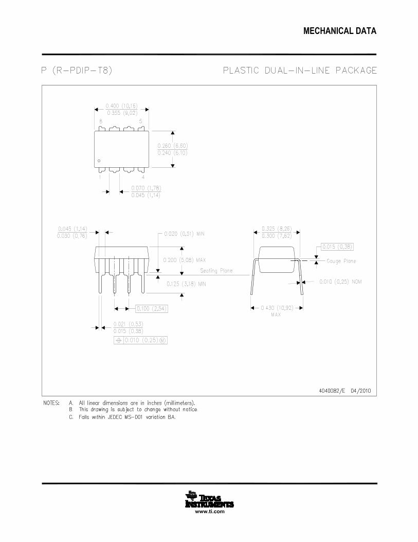
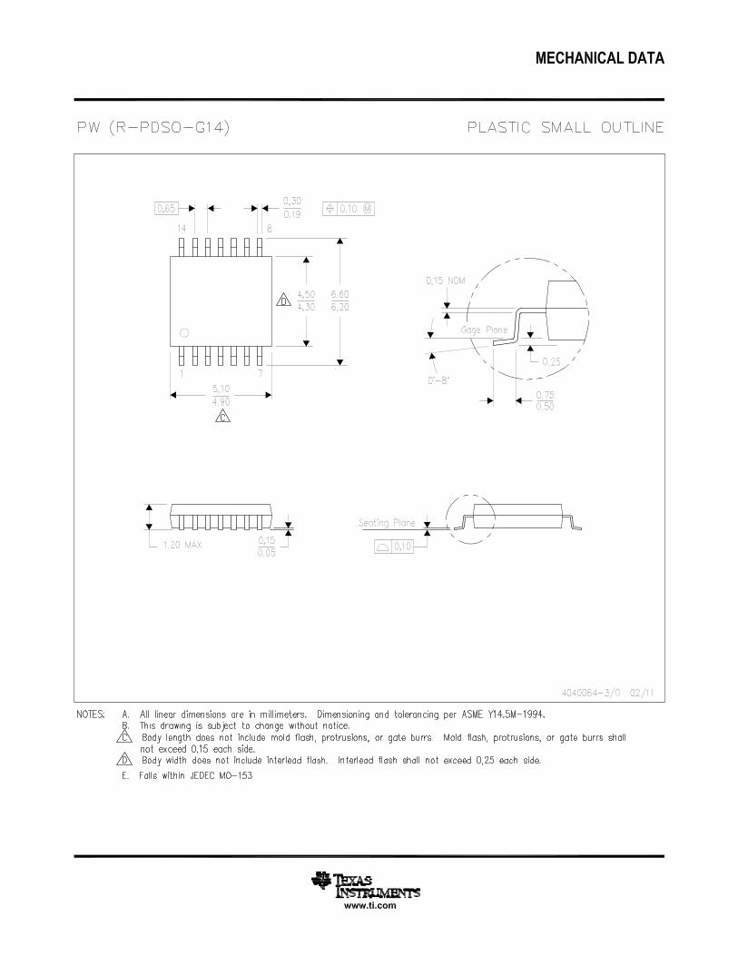
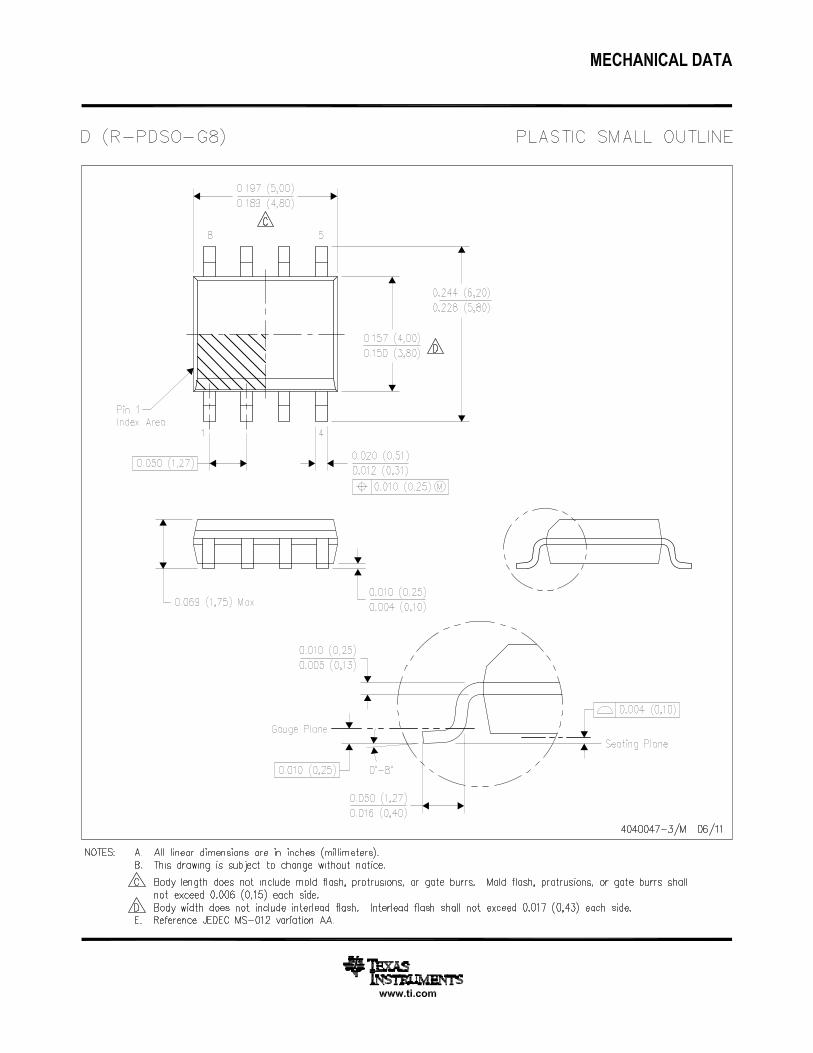
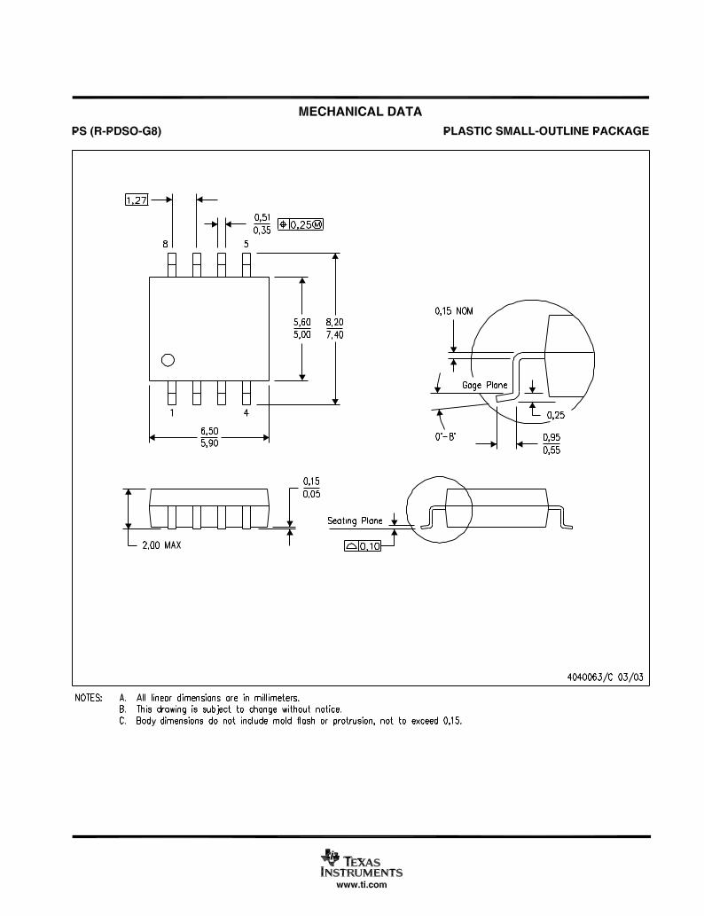
TL074A, TL074B
D, J, N, NS, OR PW PACKAGE
TL074 . . . D, J, N, NS, PW,
OR W PACKAGE
(TOP VIEW)1
2
3
4
8
7
6
5
OFFSET N1
IN−
IN+
VCC−
NC
VCC+
OUT
OFFSET N2
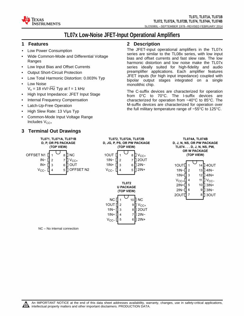
TL071, TL071A, TL071B
D, P, OR PS PACKAGE
(TOP VIEW)
1
2
3
4
8
7
6
5
1OUT
1IN−
1IN+
VCC−
VCC+
2OUT
2IN−
2IN+
TL072, TL072A, TL072B
D, JG, P, PS, OR PW PACKAGE
(TOP VIEW)
TL072
U PACKAGE
(TOP VIEW)
1
2
3
4
5
10
9
8
7
6
NC
1OUT
1IN−
1IN+
VCC−
NC
VCC+
2OUT
2IN−
2IN+
TL071, TL071A, TL071BTL072, TL072A, TL072B, TL074, TL074A, TL074B
SLOS080L –SEPTEMBER 1978–REVISED FEBRUARY 2014
TL07x Low-Noise JFET-Input Operational Amplifiers1 Features 2 Description
The JFET-input operational amplifiers in the TL07x1• Low Power Consumption
series are similar to the TL08x series, with low input• Wide Common-Mode and Differential Voltage bias and offset currents and fast slew rate. The lowRanges harmonic distortion and low noise make the TL07x
• Low Input Bias and Offset Currents series ideally suited for high-fidelity and audiopreamplifier applications. Each amplifier features• Output Short-Circuit ProtectionJFET inputs (for high input impedance) coupled with• Low Total Harmonic Distortion: 0.003% Typ bipolar output stages integrated on a single
• Low Noise monolithic chip.Vn = 18 nV/√Hz Typ at f = 1 kHz
The C-suffix devices are characterized for operation• High Input Impedance: JFET Input Stage from 0°C to 70°C. The I-suffix devices are• Internal Frequency Compensation characterized for operation from −40°C to 85°C. The
M-suffix devices are characterized for operation over• Latch-Up-Free Operationthe full military temperature range of −55°C to 125°C.• High Slew Rate: 13 V/μs Typ
• Common-Mode Input Voltage RangeIncludes VCC+
3 Terminal Out Drawings
NC – No internal connection
1
An IMPORTANT NOTICE at the end of this data sheet addresses availability, warranty, changes, use in safety-critical applications,intellectual property matters and other important disclaimers. PRODUCTION DATA.
TL071, TL071A, TL071BTL072, TL072A, TL072B, TL074, TL074A, TL074BSLOS080L –SEPTEMBER 1978–REVISED FEBRUARY 2014 www.ti.com
Table of Contents6.5 Operating Characteristics ........................................ 71 Features ................................................................. 1
7 Parameter Measurement Information ................. 82 Description ............................................................ 18 Typical Characteristics ........................................ 93 Terminal Out Drawings ........................................ 19 Application Information ..................................... 154 Revision History ................................................... 210 Device and Documentation Support ................ 175 Terminal Configuration and Functions ............... 3
10.1 Related Links ....................................................... 176 Specifications ........................................................ 510.2 Trademarks .......................................................... 176.1 Absolute Maximum Ratings ..................................... 510.3 Electrostatic Discharge Caution ........................... 176.2 Handling Ratings ...................................................... 510.4 Glossary ............................................................... 176.3 Electrical Characteristics .......................................... 6
11 Mechanical, Packaging, and Orderable6.4 Electrical Characteristics .......................................... 7Information .......................................................... 17
4 Revision HistoryNOTE: Page numbers for previous revisions may differ from page numbers in the current version.
Changes from Revision J (March 2005) to Revision K Page
• Updated document to new TI datasheet format - no specification changes. ........................................................................ 1• Added ESD warning. ........................................................................................................................................................... 17
Changes from Revision K (January 2014) to Revision L Page
• Moved Tstg to Handling Ratings table. ................................................................................................................................... 5• Added missing Electrical Characteristics table. ..................................................................................................................... 6• Added Device and Documentation Support section. ........................................................................................................... 17• Added Mechanical, Packaging, and Orderable Information section. ................................................................................... 17
2 Submit Documentation Feedback Copyright © 1978–2014, Texas Instruments Incorporated
Product Folder Links: TL071 TL071A TL071B TL072 TL072A TL072B TL074 TL074A TL074B
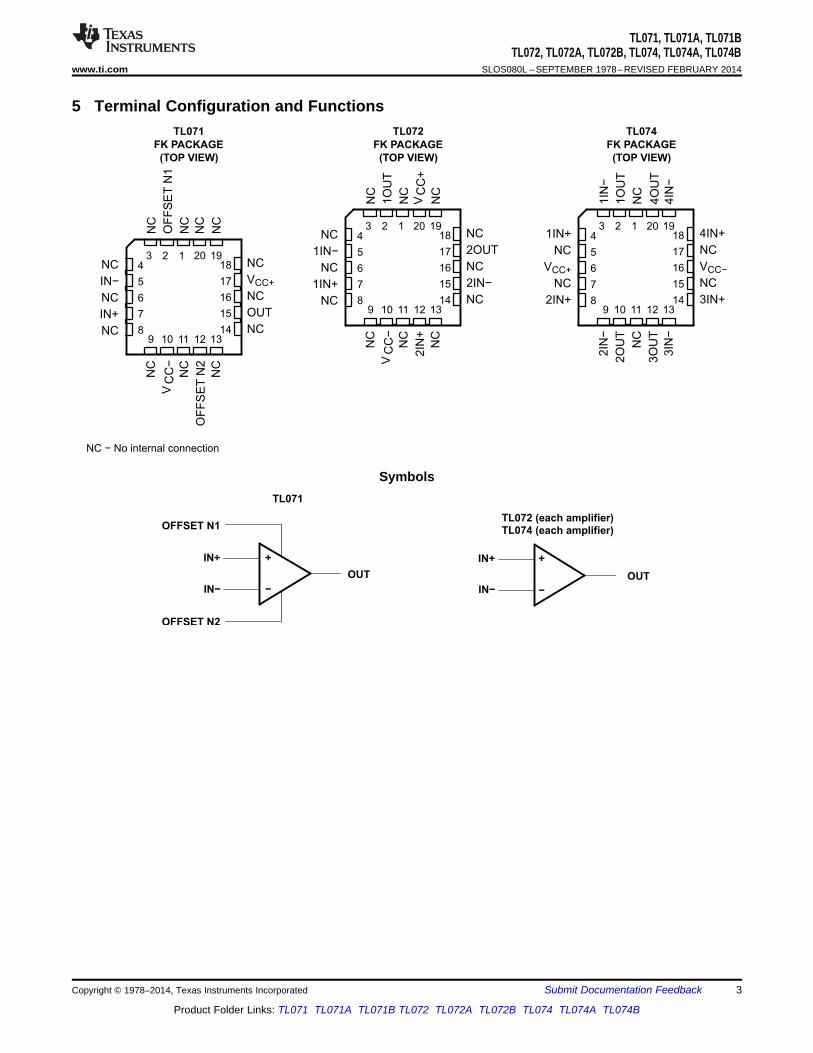
+
−
+
−
IN+
IN−
OUT
IN+
IN−
OUT
TL072 (each amplifier)TL074 (each amplifier)
TL071
OFFSET N1
OFFSET N2
NC
2OUT
NC
2IN−
NC
1IN+
NC
VCC+
NC
2IN+
NC
VCC+
NC
OUT
NC
3 2 1 20 19
9 10 11 12 13
4
5
6
7
8
18
17
16
15
14
NC
1IN−
NC
1IN+
NC
(TOP VIEW)
NC
1O
UT
NC
NC
NC
NC
NC
2IN
+
CC
−V
CC
+V
NC − No internal connection
3 2 1 20 19
9 10 11 12 13
4
5
6
7
8
18
17
16
15
14
NC
IN−
NC
IN+
NC
TL071
FK PACKAGE
(TOP VIEW)N
C
OF
FS
ET
N1
NC
NC
NC
NC
NC
OF
FS
ET
N2
NC
CC
−V
TL072
FK PACKAGE
3 2 1 20 19
9 10 11 12 13
4
5
6
7
8
18
17
16
15
14
4IN+
NC
VCC−
NC
3IN+
TL074
FK PACKAGE
(TOP VIEW)
1IN
−
1O
UT
NC
3IN
−4IN
−
2IN
−
NC
3O
UT
4O
UT
2O
UT
TL071, TL071A, TL071BTL072, TL072A, TL072B, TL074, TL074A, TL074B
www.ti.com SLOS080L –SEPTEMBER 1978–REVISED FEBRUARY 2014
5 Terminal Configuration and Functions
Symbols
Copyright © 1978–2014, Texas Instruments Incorporated Submit Documentation Feedback 3
Product Folder Links: TL071 TL071A TL071B TL072 TL072A TL072B TL074 TL074A TL074B
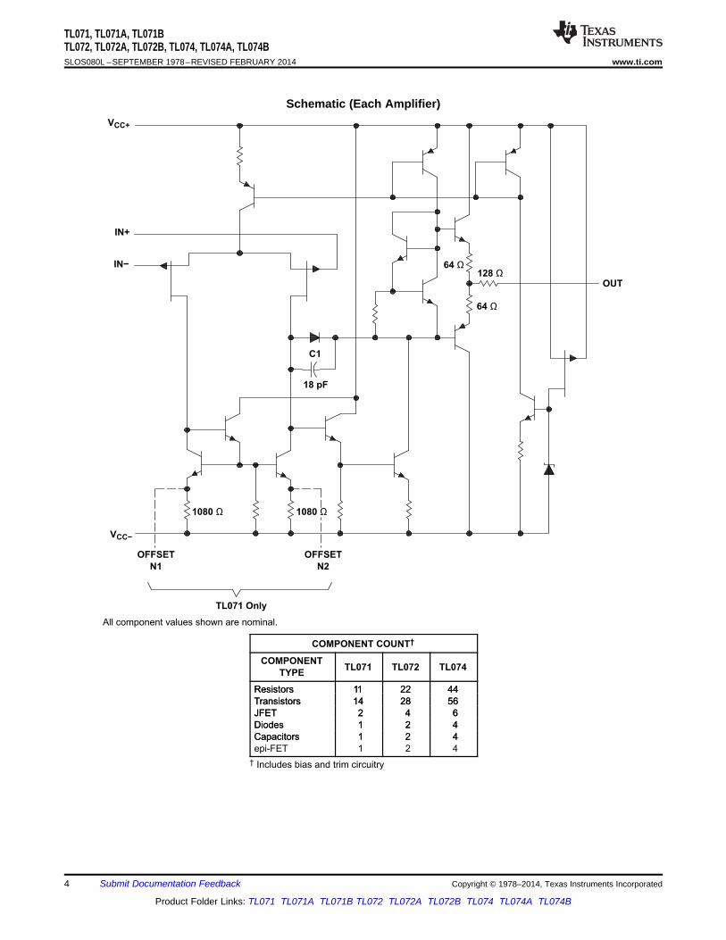
C1
VCC+
IN+
VCC−
1080 Ω 1080 Ω
IN−
TL071 Only
64 Ω128 Ω
64 Ω
All component values shown are nominal.
OFFSET
N1
OFFSET
N2
OUT
18 pF
COMPONENT COUNT†
COMPONENT
TYPETL071 TL072 TL074
Resistors 11 22 44Resistors
Transistors
11
14
22
28
44
56Transistors
JFET
14
2
28
4
56
6JFET
Diodes
2
1
4
2
6
4Diodes
Capacitors
1
1
2
2
4
4Capacitors
epi-FET
1
1
2
2
4
4
† Includes bias and trim circuitry
TL071, TL071A, TL071BTL072, TL072A, TL072B, TL074, TL074A, TL074BSLOS080L –SEPTEMBER 1978–REVISED FEBRUARY 2014 www.ti.com
Schematic (Each Amplifier)
4 Submit Documentation Feedback Copyright © 1978–2014, Texas Instruments Incorporated
Product Folder Links: TL071 TL071A TL071B TL072 TL072A TL072B TL074 TL074A TL074B
TL071, TL071A, TL071BTL072, TL072A, TL072B, TL074, TL074A, TL074B
www.ti.com SLOS080L –SEPTEMBER 1978–REVISED FEBRUARY 2014
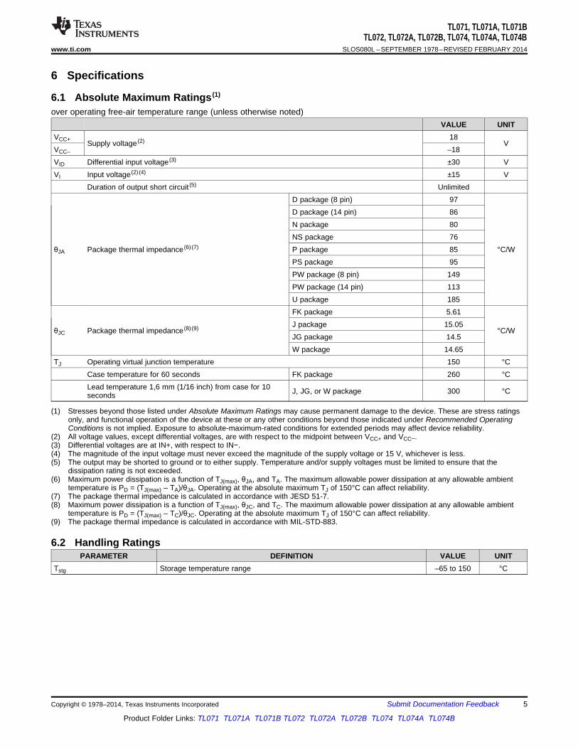
6 Specifications
6.1 Absolute Maximum Ratings (1)
over operating free-air temperature range (unless otherwise noted)VALUE UNIT
VCC+ 18Supply voltage (2) V
VCC– –18VID Differential input voltage (3) ±30 VVI Input voltage (2) (4) ±15 V
Duration of output short circuit (5) UnlimitedD package (8 pin) 97D package (14 pin) 86N package 80NS package 76
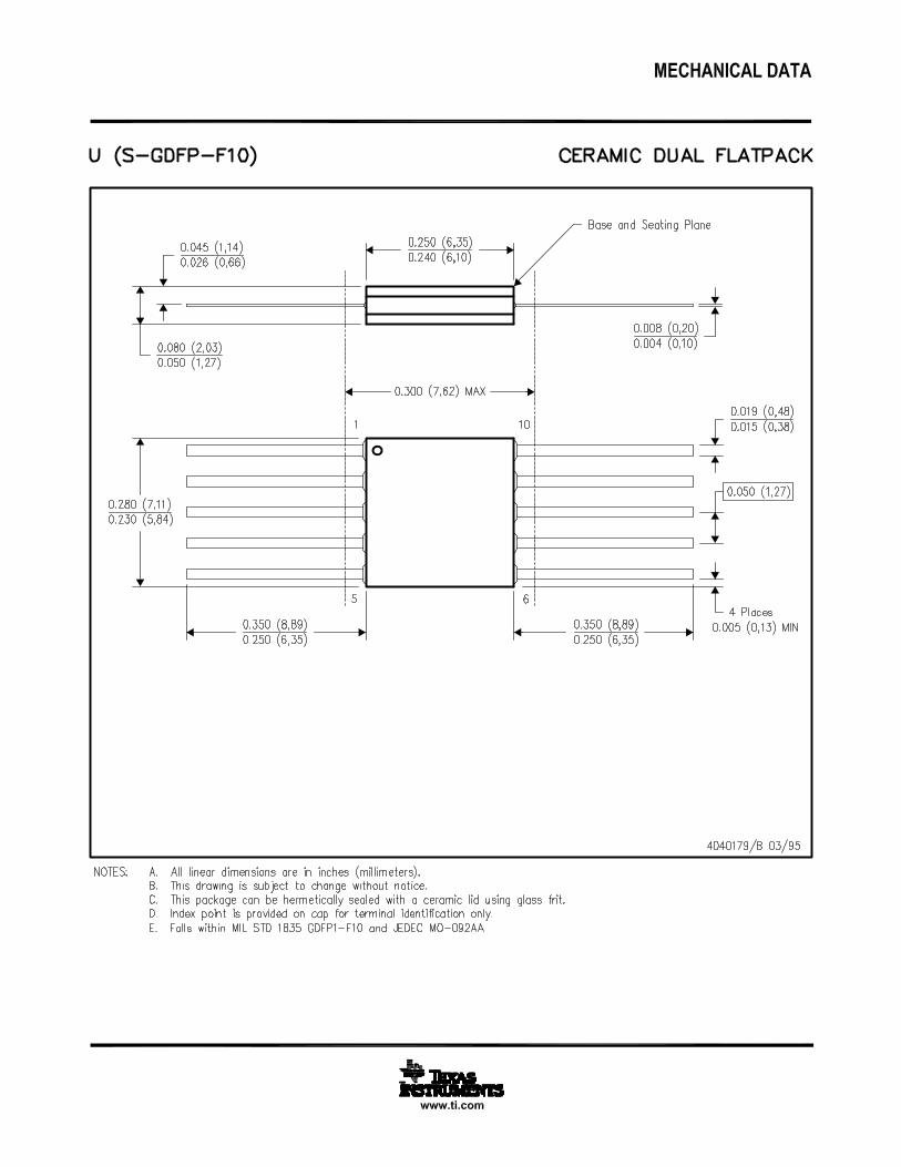
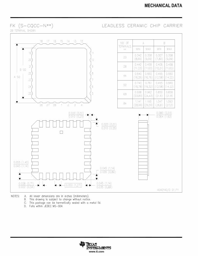
θJA Package thermal impedance (6) (7) P package 85 °C/WPS package 95PW package (8 pin) 149PW package (14 pin) 113U package 185FK package 5.61J package 15.05
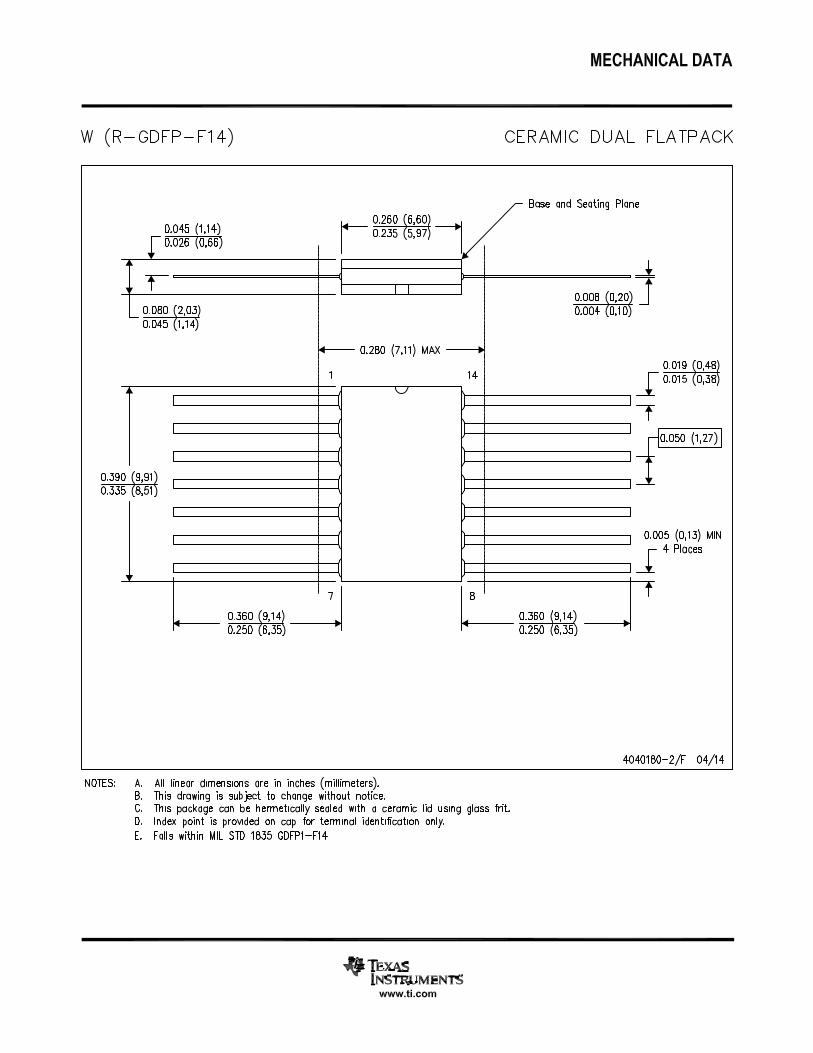
θJC Package thermal impedance (8) (9) °C/WJG package 14.5W package 14.65
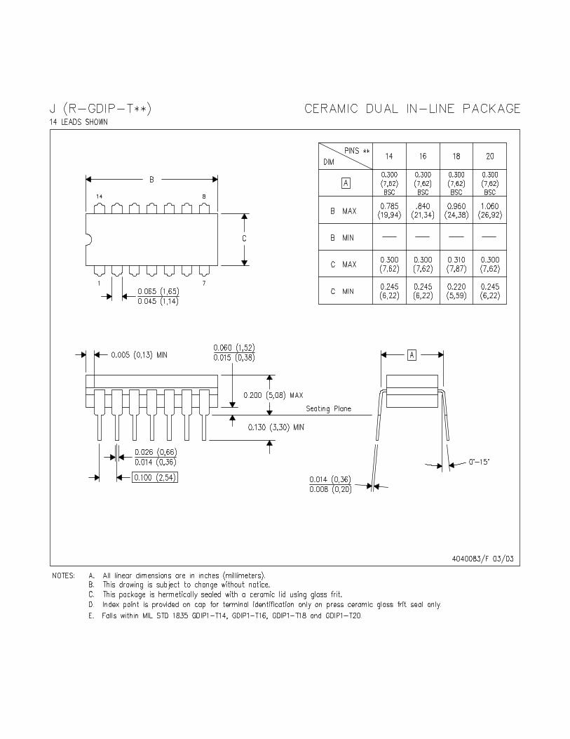
TJ Operating virtual junction temperature 150 °CCase temperature for 60 seconds FK package 260 °CLead temperature 1,6 mm (1/16 inch) from case for 10 J, JG, or W package 300 °Cseconds
(1) Stresses beyond those listed under Absolute Maximum Ratings may cause permanent damage to the device. These are stress ratingsonly, and functional operation of the device at these or any other conditions beyond those indicated under Recommended OperatingConditions is not implied. Exposure to absolute-maximum-rated conditions for extended periods may affect device reliability.
(2) All voltage values, except differential voltages, are with respect to the midpoint between VCC+ and VCC−.(3) Differential voltages are at IN+, with respect to IN−.(4) The magnitude of the input voltage must never exceed the magnitude of the supply voltage or 15 V, whichever is less.(5) The output may be shorted to ground or to either supply. Temperature and/or supply voltages must be limited to ensure that the
dissipation rating is not exceeded.(6) Maximum power dissipation is a function of TJ(max), θJA, and TA. The maximum allowable power dissipation at any allowable ambient
temperature is PD = (TJ(max) – TA)/θJA. Operating at the absolute maximum TJ of 150°C can affect reliability.(7) The package thermal impedance is calculated in accordance with JESD 51-7.(8) Maximum power dissipation is a function of TJ(max), θJC, and TC. The maximum allowable power dissipation at any allowable ambient
temperature is PD = (TJ(max) – TC)/θJC. Operating at the absolute maximum TJ of 150°C can affect reliability.(9) The package thermal impedance is calculated in accordance with MIL-STD-883.
6.2 Handling RatingsPARAMETER DEFINITION VALUE UNIT
Tstg Storage temperature range –65 to 150 °C
Copyright © 1978–2014, Texas Instruments Incorporated Submit Documentation Feedback 5
Product Folder Links: TL071 TL071A TL071B TL072 TL072A TL072B TL074 TL074A TL074B
TL071, TL071A, TL071BTL072, TL072A, TL072B, TL074, TL074A, TL074BSLOS080L –SEPTEMBER 1978–REVISED FEBRUARY 2014 www.ti.com
6.3 Electrical CharacteristicsVCC± = ±15 V (unless otherwise noted)
TL071C TL071AC TL071BC TL071ITL072C TL072AC TL072BC TL072ITESTPARAMETER TA
(2) UNITTL074C TL074AC TL074BC TL074ICONDITIONS(1)
MIN TYP MAX MIN TYP MAX MIN TYP MAX MIN TYP MAX
25°C 3 10 3 6 2 3 3 6Input offsetVIO VO = 0, RS = 50 Ω mVFullvoltage 13 7.5 5 8range
Temperaturecoefficient of FullVO = 0, RS = 50 Ω 18 18 18 18 µV/°CαVIO input offset rangevoltage
25°C 5 100 5 100 5 100 5 100 pAInput offsetIIO VO = 0 Fullcurrent 10 2 2 2 nArange
25°C 65 200 65 200 65 200 65 200 pAInput biasIIB VO = 0 Fullcurrent (3)
7 7 7 7 nArange
Common-mode –12 –12 –12 –12VICR input voltage 25°C ±11 to ±11 to ±11 to ±11 to V
range 15 15 15 15
RL= 10 kΩ 25°C ±12 ±13.5 ±12 ±13.5 ±12 ±13.5 ±12 ±13.5Maximum peak
VOM output voltage RL≥ 10 kΩ ±12 ±12 ±12 ±12 VFullswing rangeRL≥ 2 kΩ ±10 ±10 ±10 ±10
Large-signal 25°C 25 200 50 200 50 200 50 200differentialAVD VO = ±10 V, RL≥ 2 kΩ V/mVFullvoltage 15 25 25 25rangeamplification
Utility-gainB1 25°C 3 3 3 3 MHzbandwidth
rI Input resistance 25°C Ω1012 1012 1012 1012
VIC = VICRmin,Common-modeCMRR 25°C 70 100 75 100 75 100 75 100 dBrejection ratio VO = 0, RS = 50 Ω
Supply-voltage VCC = ±9 V to ±15 V,kSVR rejection ratio 25°C 70 100 80 100 80 100 80 100 dB
VO = 0, RS = 50 Ω(ΔVCC±/ΔVIO)
Supply currentICC VO = 0, No load 25°C 1.4 2.5 1.4 2.5 1.4 2.5 1.4 2.5 mA(each amplifier)
VO1/VO Crosstalk AVD = 100 25°C 120 120 120 120 dB2 attenuation
(1) All characteristics are measured under open-loop conditions with zero common-mode voltage, unless otherwise specified.(2) Full range is TA = 0°C to 70°C for TL07_C,TL07_AC, TL07_BC and is TA = –40°C to 85°C for TL07_I.(3) Input bias currents of an FET-input operational amplifier are normal junction reverse currents, which are temperature sensitive, as
shown in Figure 4. Pulse techniques must be used that maintain the junction temperature as close to the ambient temperature aspossible.
6 Submit Documentation Feedback Copyright © 1978–2014, Texas Instruments Incorporated
Product Folder Links: TL071 TL071A TL071B TL072 TL072A TL072B TL074 TL074A TL074B
TL071, TL071A, TL071BTL072, TL072A, TL072B, TL074, TL074A, TL074B
www.ti.com SLOS080L –SEPTEMBER 1978–REVISED FEBRUARY 2014
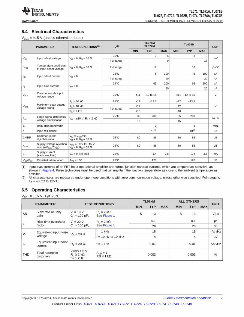
6.4 Electrical CharacteristicsVCC± = ±15 V (unless otherwise noted)
TL071M TL074MTL072MPARAMETER TEST CONDITIONS (1) TA(2) UNIT
MIN TYP MAX MIN TYP MAX
25°C 3 6 3 9VIO Input offset voltage VO = 0, RS = 50 Ω mV
Full range 9 15
Temperature coefficientαVIO VO = 0, RS = 50 Ω Full range 18 18 μV/°Cof input offset voltage
25°C 5 100 5 100 pAIIO Input offset current VO = 0
Full range 20 20 nA
25°C 65 200 65 200 pAIIB Input bias current VO = 0
50 20 nA
Common-mode inputVICR 25°C ±11 –12 to 15 ±11 –12 to 15 Vvoltage range
RL = 10 kΩ 25°C ±12 ±13.5 ±12 ±13.5Maximum peak outputVOM RL ≥ 10 kΩ ±12 ±12 Vvoltage swing Full range
RL ≥ 2 kΩ ±10 ±10
25°C 35 200 35 200Large-signal differentialAVD VO = ±10 V, RL ≥ 2 kΩ V/mVvoltage amplification 15 15
B1 Unity-gain bandwidth 3 3 MHz
ri Input resistance Ω1012 1012
Common-mode VIC = VICRmin,CMRR 25°C 80 86 80 86 dBrejection ratio VO = 0, RS = 50 Ω
Supply-voltage rejection VCC = ±9 V to ±15 V,kSVR 25°C 80 86 80 86 dBratio (ΔVCC±/ΔVIO) VO = 0, RS = 50 Ω
Supply currentICC VO = 0, No load 25°C 1.4 2.5 1.4 2.5 mA(each amplifier)
VO1/VO2 Crosstalk attenuation AVD = 100 25°C 120 120 dB
(1) Input bias currents of an FET-input operational amplifier are normal junction reverse currents, which are temperature sensitive, asshown in Figure 4. Pulse techniques must be used that will maintain the junction temperature as close to the ambient temperature aspossible.
(2) All characteristics are measured under open-loop conditions with zero common-mode voltage, unless otherwise specified. Full range isTA = –55°C to 125°C.
6.5 Operating CharacteristicsVCC± = ±15 V, TA= 25°C
TL07xM ALL OTHERSPARAMETER TEST CONDITIONS UNIT
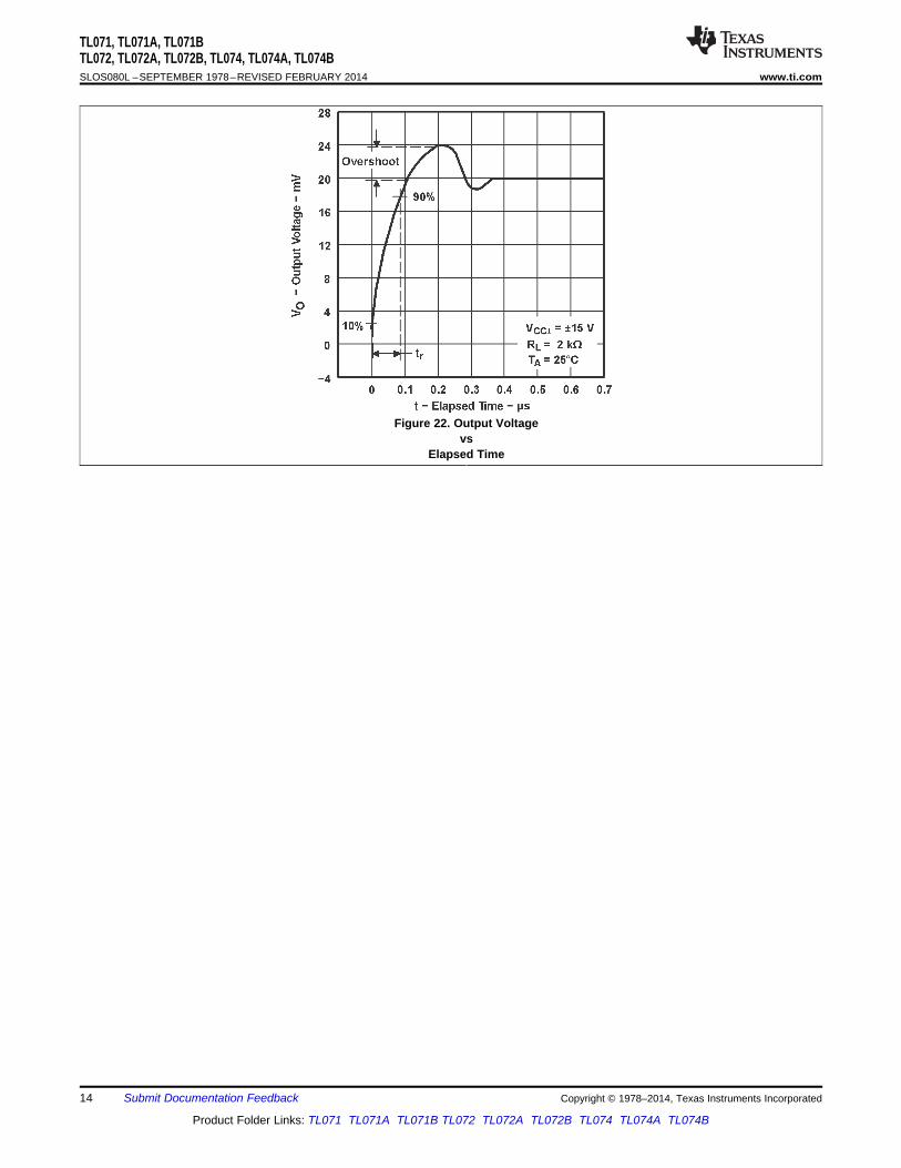
MIN TYP MAX MIN TYP MAXSlew rate at unity VI = 10 V, RL = 2 kΩ,SR 5 13 8 13 V/μsgain CL = 100 pF, See Figure 1
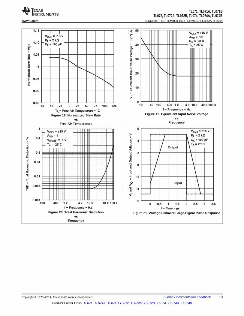
0.1 0.1 μsRise-time overshoot VI = 20 V, RL = 2 kΩ,tr factor CL = 100 pF, See Figure 1 20 20 %f = 1 kHz 18 18 nV/√HzEquivalent input noiseVn RS = 20 Ωvoltage f = 10 Hz to 10 kHz 4 4 μV
Equivalent input noiseIn RS = 20 Ω, f = 1 kHz 0.01 0.01 pA/√HzcurrentVIrms = 6 V,Total harmonic AVD = 1,THD RL ≥ 2 kΩ, 0.003 0.003 %distortion RS ≤ 1 kΩ,f = 1 kHz,
Copyright © 1978–2014, Texas Instruments Incorporated Submit Documentation Feedback 7
Product Folder Links: TL071 TL071A TL071B TL072 TL072A TL072B TL074 TL074A TL074B
N1
100 kΩ
+
− TL071
N2
1.5 kΩ
VCC−
OUT
IN−
IN+
VI
−
CL = 100 pF RL = 2 kΩ
VO
+
VI
+
−
10 kΩ
1 kΩ
RL CL = 100 pF
VO
TL071, TL071A, TL071BTL072, TL072A, TL072B, TL074, TL074A, TL074BSLOS080L –SEPTEMBER 1978–REVISED FEBRUARY 2014 www.ti.com
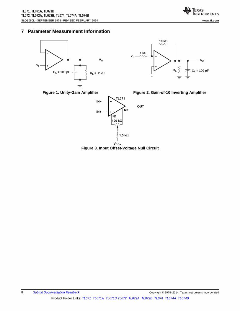
7 Parameter Measurement Information
Figure 1. Unity-Gain Amplifier Figure 2. Gain-of-10 Inverting Amplifier
Figure 3. Input Offset-Voltage Null Circuit
8 Submit Documentation Feedback Copyright © 1978–2014, Texas Instruments Incorporated
Product Folder Links: TL071 TL071A TL071B TL072 TL072A TL072B TL074 TL074A TL074B
IIB
−In
pu
t B
ias C
urr
en
t−
nA
TA − Free-Air Temperature − °C
IBI
10
1
0.1
0.01
100
−75 −50 −25 0 25 50 75 100 125
VCC± = ±15 V RL = 10 kΩ
TA = 25°C
See Figure 2
±15
±12.5
±10
±7.5
±5
±2.5
0
VO
M−
Maxim
um
Peak
Ou
tpu
t Vo
ltag
e−
V
f − Frequency − Hz
100 1 k 10 k 100 k 1 M 10 M
VO
M
VCC± = ±5 V
VCC± = ±10 V
VCC± = ±15 V
TL071, TL071A, TL071BTL072, TL072A, TL072B, TL074, TL074A, TL074B
www.ti.com SLOS080L –SEPTEMBER 1978–REVISED FEBRUARY 2014
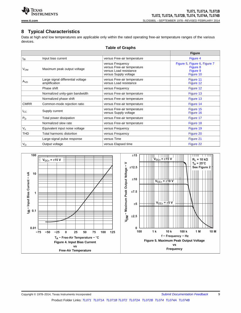
8 Typical CharacteristicsData at high and low temperatures are applicable only within the rated operating free-air temperature ranges of the variousdevices.
Table of GraphsFigure
IIB Input bias current versus Free-air temperature Figure 4versus Frequency Figure 5, Figure 6, Figure 7versus Free-air temperature Figure 8VOM Maximum peak output voltage versus Load resistance Figure 9versus Supply voltage Figure 10
Large signal differential voltage versus Free-air temperature Figure 11AVD amplification versus Load resistance Figure 12Phase shift versus Frequency Figure 12Normalized unity-gain bandwidth versus Free-air temperature Figure 13Normalized phase shift versus Free-air temperature Figure 13
CMRR Common-mode rejection ratio versus Free-air temperature Figure 14versus Free-air temperature Figure 15ICC Supply current versus Supply voltage Figure 16
PD Total power dissipation versus Free-air temperature Figure 17Normalized slew rate versus Free-air temperature Figure 18
Vn Equivalent input noise voltage versus Frequency Figure 19THD Total harmonic distortion versus Frequency Figure 20
Large-signal pulse response versus Time Figure 21VO Output voltage versus Elapsed time Figure 22
Figure 5. Maximum Peak Output VoltageFigure 4. Input Bias Currentvsvs
FrequencyFree-Air Temperature
Copyright © 1978–2014, Texas Instruments Incorporated Submit Documentation Feedback 9
Product Folder Links: TL071 TL071A TL071B TL072 TL072A TL072B TL074 TL074A TL074B
−750
VO
M−
Maxim
um
Peak O
utp
ut
Vo
ltag
e−
V
TA − Free-Air Temperature − °C
125
±15
−50 −25 0 25 50 75 100
±2.5
±5
±7.5
±10
±12.5
RL = 10 kΩ
VCC± = ±15 V
See Figure 2
VO
M
RL = 2 kΩ
8
0.10
RL − Load Resistance − kΩ
10
±15
±2.5
±5
±7.5
±10
±12.5
VCC± = ±15 V
TA = 25°C
See Figure 2
0.2 0.4 0.7 1 2 4 7
VO
M−
Maxim
um
Peak
Ou
tpu
t Vo
ltag
e−
VVO
M
8
10 M1 M100 k10 k1 k100
f − Frequency − Hz
VO
M−
Maxim
um
Peak
Ou
tpu
t Vo
ltag
e−
V
0
±2.5
±5
±7.5
±10
±12.5
±15
See Figure 2
TA = 25°C
RL = 2 kΩ
VCC± = ±10 V
VCC± = ±5 V
VO
M
VCC± = ±15 V
8
TL071, TL071A, TL071BTL072, TL072A, TL072B, TL074, TL074A, TL074BSLOS080L –SEPTEMBER 1978–REVISED FEBRUARY 2014 www.ti.com
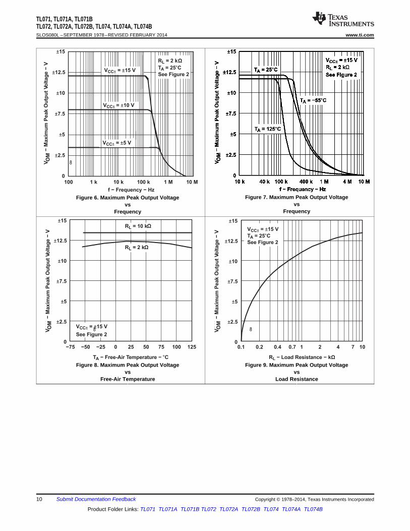
Figure 7. Maximum Peak Output VoltageFigure 6. Maximum Peak Output Voltagevsvs
FrequencyFrequency
Figure 8. Maximum Peak Output Voltage Figure 9. Maximum Peak Output Voltagevs vs
Free-Air Temperature Load Resistance
10 Submit Documentation Feedback Copyright © 1978–2014, Texas Instruments Incorporated
Product Folder Links: TL071 TL071A TL071B TL072 TL072A TL072B TL074 TL074A TL074B
1.02
1.01
1
0.99
0.98
1.03
0.97
−750.7
No
rmalized
Un
ity-G
ain
Ban
dw
idth
TA − Free-Air Temperature − °C
125
1.3
−50 −25 0 25 50 75 100
0.8
0.9
1
1.1
1.2 Unity-Gain Bandwidth
VCC± = ±15 V
RL = 2 kΩ
f = B1 for Phase Shift
Phase Shift
No
rmalized
Ph
ase S
hif
t
00
VO
M−
Maxim
um
Peak O
utp
ut
Vo
ltag
e−
V
|VCC±| − Supply Voltage − V
16
±15
2 4 6 8 10 12 14
±2.5
±5
±7.5
±10
±12.5
RL = 10 kΩ
TA = 25°C
VO
M
−751
Vo
ltag
eA
mp
lifi
cati
on
−V
/mV
TA − Free-Air Temperature − °C
125
1000
−50 −25 0 25 50 75 100
2
4
10
20
40
100
200
400
VCC± = ±15 V
VO = ±10 VRL = 2 kΩ
AV
D−
Larg
e-S
ign
al D
iffe
ren
tial
AV
D
TL071, TL071A, TL071BTL072, TL072A, TL072B, TL074, TL074A, TL074B
www.ti.com SLOS080L –SEPTEMBER 1978–REVISED FEBRUARY 2014
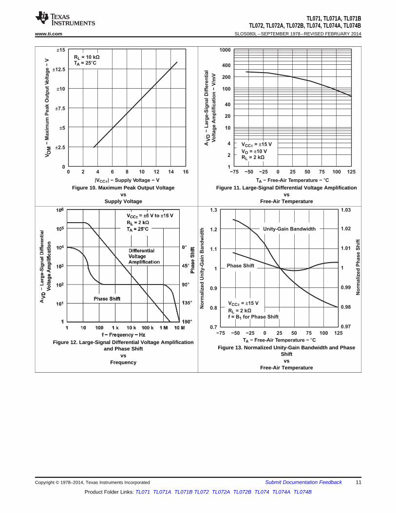
Figure 10. Maximum Peak Output Voltage Figure 11. Large-Signal Differential Voltage Amplificationvs vs
Supply Voltage Free-Air Temperature
Figure 12. Large-Signal Differential Voltage AmplificationFigure 13. Normalized Unity-Gain Bandwidth and Phaseand Phase Shift
ShiftvsvsFrequency
Free-Air Temperature
Copyright © 1978–2014, Texas Instruments Incorporated Submit Documentation Feedback 11
Product Folder Links: TL071 TL071A TL071B TL072 TL072A TL072B TL074 TL074A TL074B
−750
TA − Free-Air Temperature − °C
125
2
−50 −25 0 25 50 75 100
0.2
0.4
0.6
0.8
1
1.2
1.4
1.6
1.8
VCC± = ±15 V
No Signal
No Load
ICC
−S
up
ply
Cu
rren
t P
erA
mp
lifi
er
−m
AC
C±
I
−750
TA − Free-Air Temperature −C°
125
250
−50 −25 0 25 50 75 100
25
50
75
100
125
150
175
200
225VCC± = 15 V±
No SignalNo Load
TL074
TL071
TL072
−To
tal
Po
wer
Dis
sip
ati
on
−m
WP
D
−7583
CM
RR
−C
om
mo
n-M
od
e R
eje
cti
on
Rati
o−
dB
TA − Free-Air Temperature − °C
125
89
−50 −25 0 25 50 75 100
84
85
86
87
88
VCC± = ±15 V
RL = 10 kΩ
00
|VCC±| − Supply Voltage − V
16
2
2 4 6 8 10 12 14
0.2
0.4
0.6
0.8
1
1.2
1.4
1.6
1.8TA = 25°C
No SignalNo Load
ICC
−S
up
ply
Cu
rren
t P
erA
mp
lifi
er
−m
AC
C±
I
TL071, TL071A, TL071BTL072, TL072A, TL072B, TL074, TL074A, TL074BSLOS080L –SEPTEMBER 1978–REVISED FEBRUARY 2014 www.ti.com
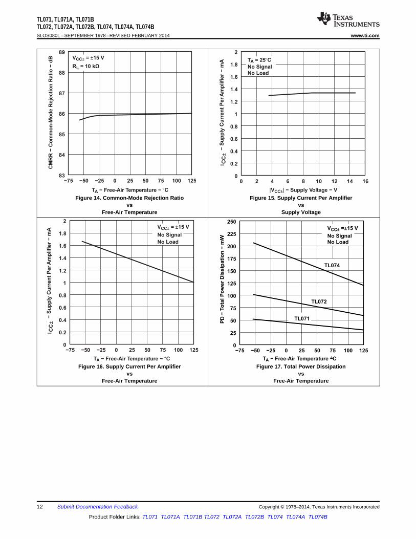
Figure 14. Common-Mode Rejection Ratio Figure 15. Supply Current Per Amplifiervs vs
Free-Air Temperature Supply Voltage
Figure 16. Supply Current Per Amplifier Figure 17. Total Power Dissipationvs vs
Free-Air Temperature Free-Air Temperature
12 Submit Documentation Feedback Copyright © 1978–2014, Texas Instruments Incorporated
Product Folder Links: TL071 TL071A TL071B TL072 TL072A TL072B TL074 TL074A TL074B
−6
t − Time − µs
3.5
6
0 0.5 1 1.5 2 2.5 3
−4
−2
0
2
4
Output
Input
VCC± = ±15 V
RL = 2 kΩ
TA = 25°C
CL = 100 pF
VO
VI
−In
pu
t an
d O
utp
ut
Vo
ltag
es
−V
an
d
0.001
TH
D−
To
tal
Harm
on
ic D
isto
rtio
n−
%
1
40 k10 k4 k1 k400 100 k
f − Frequency − Hz
100
0.004
0.01
0.04
0.1
0.4
VCC± = ±15 V
AVD = 1
VI(RMS) = 6 V
TA = 25°C
100
−E
qu
ivale
nt
Inp
ut
No
ise
Vo
ltag
e−
nV
/Hz
f − Frequency − Hz
100 k
50
10
20
30
40
VCC± = ±15 V
AVD = 10
RS = 20 Ω
TA = 25°C
40 100 400 1 k 4 k 10 k 40 k
nV
/H
zV
n
TL071, TL071A, TL071BTL072, TL072A, TL072B, TL074, TL074A, TL074B
www.ti.com SLOS080L –SEPTEMBER 1978–REVISED FEBRUARY 2014
Figure 19. Equivalent Input Noise VoltageFigure 18. Normalized Slew Ratevsvs
FrequencyFree-Air Temperature
Figure 20. Total Harmonic Distortion Figure 21. Voltage-Follower Large-Signal Pulse Responsevs
Frequency
Copyright © 1978–2014, Texas Instruments Incorporated Submit Documentation Feedback 13
Product Folder Links: TL071 TL071A TL071B TL072 TL072A TL072B TL074 TL074A TL074B
TL071, TL071A, TL071BTL072, TL072A, TL072B, TL074, TL074A, TL074BSLOS080L –SEPTEMBER 1978–REVISED FEBRUARY 2014 www.ti.com
Figure 22. Output Voltagevs
Elapsed Time
14 Submit Documentation Feedback Copyright © 1978–2014, Texas Instruments Incorporated
Product Folder Links: TL071 TL071A TL071B TL072 TL072A TL072B TL074 TL074A TL074B
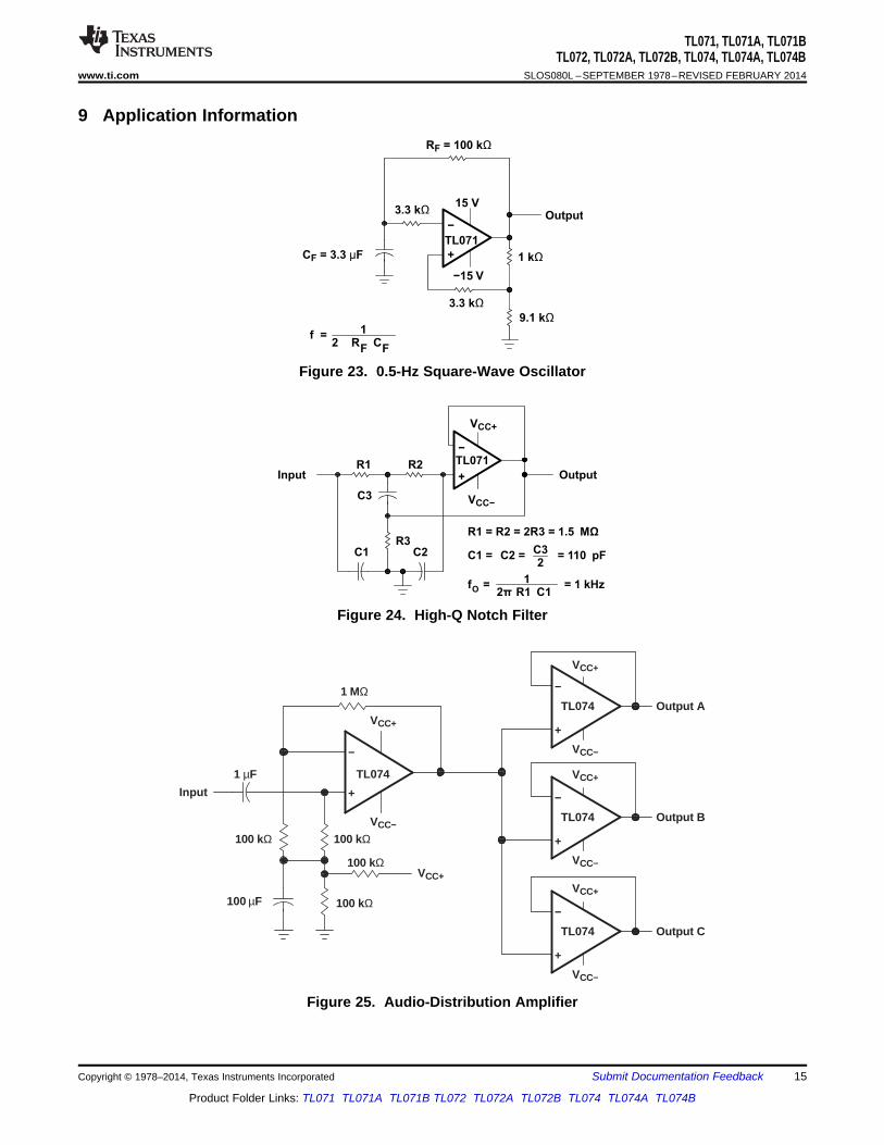
100 µF
+
−
+
−
TL074 Output C
VCC+
VCC+
Output BTL074
−
+
VCC+
Output ATL074
−
+VCC+
TL074
VCC+100 kΩ
Input
1 µF
1 MΩ
100 kΩ
100 kΩVCC−
100 kΩ
VCC−
VCC−
VCC−
+
−
R2R1
C1 C2R3
C3 VCC−
VCC+
TL071
OutputInput
C1 = C2 =C32
= 110 pF
fO = 12π R1 C1
= 1 kHz
R1 = R2 = 2R3 = 1.5 MΩ
+
−
−15 V
15 VOutput
1 kΩ
9.1 kΩ
3.3 kΩ
CF = 3.3 µF
RF = 100 kΩ
3.3 kΩ
TL071
f = 12 R
FC
F
TL071, TL071A, TL071BTL072, TL072A, TL072B, TL074, TL074A, TL074B
www.ti.com SLOS080L –SEPTEMBER 1978–REVISED FEBRUARY 2014
9 Application Information
Figure 23. 0.5-Hz Square-Wave Oscillator
Figure 24. High-Q Notch Filter
Figure 25. Audio-Distribution Amplifier
Copyright © 1978–2014, Texas Instruments Incorporated Submit Documentation Feedback 15
Product Folder Links: TL071 TL071A TL071B TL072 TL072A TL072B TL074 TL074A TL074B
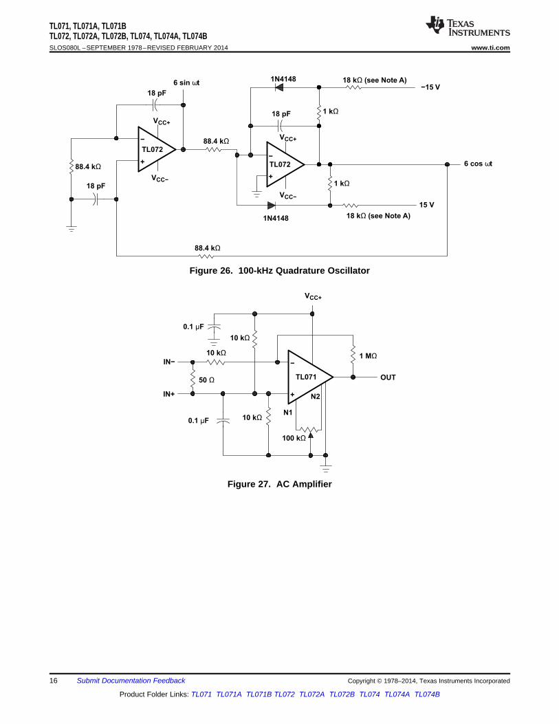
0.1 Fµ
0.1 µF
+
−
10 kΩ
50 Ω
100 kΩ
N1
OUT
1 MΩ
VCC+
10 kΩ
10 kΩ
TL071
N2
IN−
IN+
−15 V6 sin ωt
+
−
6 cos ωt
+
−
88.4 kΩ
VCC+
VCC−
VCC+
VCC−
1N4148
18 pF
18 pF
1 kΩ
18 kΩ (see Note A)
15 V
TL072
TL072
88.4 kΩ
88.4 kΩ
18 pF
1 kΩ
18 kΩ (see Note A)1N4148
TL071, TL071A, TL071BTL072, TL072A, TL072B, TL074, TL074A, TL074BSLOS080L –SEPTEMBER 1978–REVISED FEBRUARY 2014 www.ti.com
Figure 26. 100-kHz Quadrature Oscillator
Figure 27. AC Amplifier
16 Submit Documentation Feedback Copyright © 1978–2014, Texas Instruments Incorporated
Product Folder Links: TL071 TL071A TL071B TL072 TL072A TL072B TL074 TL074A TL074B
TL071, TL071A, TL071BTL072, TL072A, TL072B, TL074, TL074A, TL074B
www.ti.com SLOS080L –SEPTEMBER 1978–REVISED FEBRUARY 2014
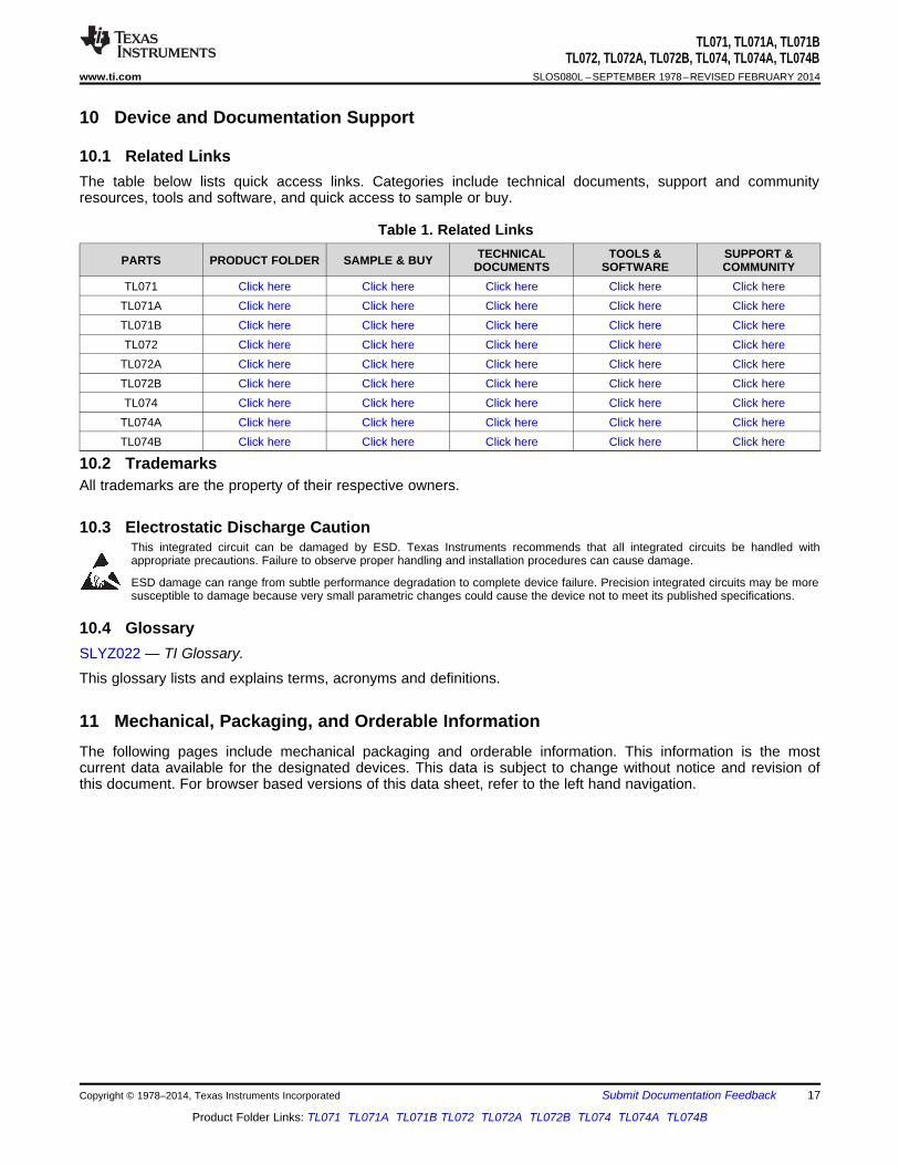
10 Device and Documentation Support
10.1 Related LinksThe table below lists quick access links. Categories include technical documents, support and communityresources, tools and software, and quick access to sample or buy.
Table 1. Related LinksTECHNICAL TOOLS & SUPPORT &PARTS PRODUCT FOLDER SAMPLE & BUY DOCUMENTS SOFTWARE COMMUNITY
TL071 Click here Click here Click here Click here Click hereTL071A Click here Click here Click here Click here Click hereTL071B Click here Click here Click here Click here Click hereTL072 Click here Click here Click here Click here Click here
TL072A Click here Click here Click here Click here Click hereTL072B Click here Click here Click here Click here Click hereTL074 Click here Click here Click here Click here Click here
TL074A Click here Click here Click here Click here Click hereTL074B Click here Click here Click here Click here Click here
10.2 TrademarksAll trademarks are the property of their respective owners.
10.3 Electrostatic Discharge CautionThis integrated circuit can be damaged by ESD. Texas Instruments recommends that all integrated circuits be handled withappropriate precautions. Failure to observe proper handling and installation procedures can cause damage.
ESD damage can range from subtle performance degradation to complete device failure. Precision integrated circuits may be moresusceptible to damage because very small parametric changes could cause the device not to meet its published specifications.
10.4 GlossarySLYZ022 — TI Glossary.
This glossary lists and explains terms, acronyms and definitions.
11 Mechanical, Packaging, and Orderable InformationThe following pages include mechanical packaging and orderable information. This information is the mostcurrent data available for the designated devices. This data is subject to change without notice and revision ofthis document. For browser based versions of this data sheet, refer to the left hand navigation.
Copyright © 1978–2014, Texas Instruments Incorporated Submit Documentation Feedback 17
Product Folder Links: TL071 TL071A TL071B TL072 TL072A TL072B TL074 TL074A TL074B
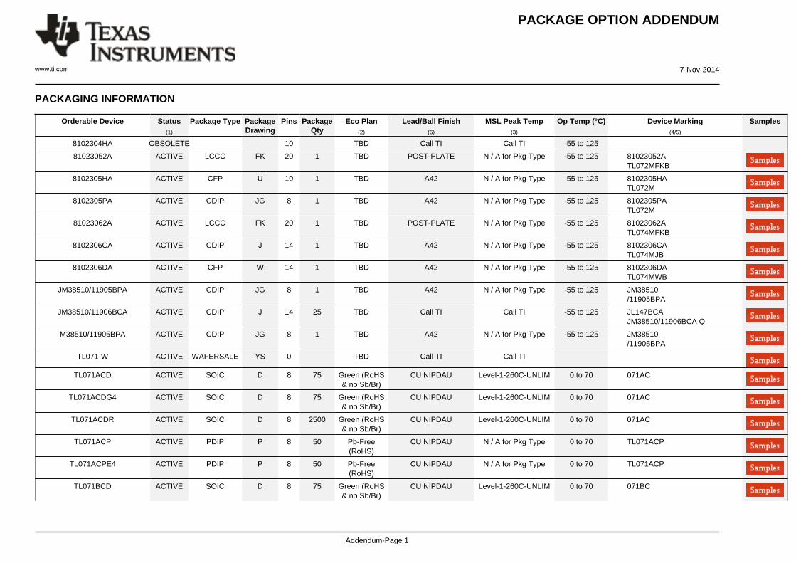
PACKAGE OPTION ADDENDUM
www.ti.com 7-Nov-2014
Addendum-Page 1
PACKAGING INFORMATION
Orderable Device Status(1)
Package Type PackageDrawing
Pins PackageQty
Eco Plan(2)
Lead/Ball Finish(6)
MSL Peak Temp(3)
Op Temp (°C) Device Marking(4/5)
Samples
8102304HA OBSOLETE 10 TBD Call TI Call TI -55 to 125
81023052A ACTIVE LCCC FK 20 1 TBD POST-PLATE N / A for Pkg Type -55 to 125 81023052ATL072MFKB
8102305HA ACTIVE CFP U 10 1 TBD A42 N / A for Pkg Type -55 to 125 8102305HATL072M
8102305PA ACTIVE CDIP JG 8 1 TBD A42 N / A for Pkg Type -55 to 125 8102305PATL072M
81023062A ACTIVE LCCC FK 20 1 TBD POST-PLATE N / A for Pkg Type -55 to 125 81023062ATL074MFKB
8102306CA ACTIVE CDIP J 14 1 TBD A42 N / A for Pkg Type -55 to 125 8102306CATL074MJB
8102306DA ACTIVE CFP W 14 1 TBD A42 N / A for Pkg Type -55 to 125 8102306DATL074MWB
JM38510/11905BPA ACTIVE CDIP JG 8 1 TBD A42 N / A for Pkg Type -55 to 125 JM38510/11905BPA
JM38510/11906BCA ACTIVE CDIP J 14 25 TBD Call TI Call TI -55 to 125 JL147BCAJM38510/11906BCA Q
M38510/11905BPA ACTIVE CDIP JG 8 1 TBD A42 N / A for Pkg Type -55 to 125 JM38510/11905BPA
TL071-W ACTIVE WAFERSALE YS 0 TBD Call TI Call TI
TL071ACD ACTIVE SOIC D 8 75 Green (RoHS& no Sb/Br)
CU NIPDAU Level-1-260C-UNLIM 0 to 70 071AC
TL071ACDG4 ACTIVE SOIC D 8 75 Green (RoHS& no Sb/Br)
CU NIPDAU Level-1-260C-UNLIM 0 to 70 071AC
TL071ACDR ACTIVE SOIC D 8 2500 Green (RoHS& no Sb/Br)
CU NIPDAU Level-1-260C-UNLIM 0 to 70 071AC
TL071ACP ACTIVE PDIP P 8 50 Pb-Free(RoHS)
CU NIPDAU N / A for Pkg Type 0 to 70 TL071ACP
TL071ACPE4 ACTIVE PDIP P 8 50 Pb-Free(RoHS)
CU NIPDAU N / A for Pkg Type 0 to 70 TL071ACP
TL071BCD ACTIVE SOIC D 8 75 Green (RoHS& no Sb/Br)
CU NIPDAU Level-1-260C-UNLIM 0 to 70 071BC
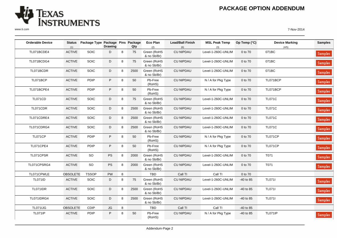
PACKAGE OPTION ADDENDUM
www.ti.com 7-Nov-2014
Addendum-Page 2
Orderable Device Status(1)
Package Type PackageDrawing
Pins PackageQty
Eco Plan(2)
Lead/Ball Finish(6)
MSL Peak Temp(3)
Op Temp (°C) Device Marking(4/5)
Samples
TL071BCDE4 ACTIVE SOIC D 8 75 Green (RoHS& no Sb/Br)
CU NIPDAU Level-1-260C-UNLIM 0 to 70 071BC
TL071BCDG4 ACTIVE SOIC D 8 75 Green (RoHS& no Sb/Br)
CU NIPDAU Level-1-260C-UNLIM 0 to 70 071BC
TL071BCDR ACTIVE SOIC D 8 2500 Green (RoHS& no Sb/Br)
CU NIPDAU Level-1-260C-UNLIM 0 to 70 071BC
TL071BCP ACTIVE PDIP P 8 50 Pb-Free(RoHS)
CU NIPDAU N / A for Pkg Type 0 to 70 TL071BCP
TL071BCPE4 ACTIVE PDIP P 8 50 Pb-Free(RoHS)
CU NIPDAU N / A for Pkg Type 0 to 70 TL071BCP
TL071CD ACTIVE SOIC D 8 75 Green (RoHS& no Sb/Br)
CU NIPDAU Level-1-260C-UNLIM 0 to 70 TL071C
TL071CDR ACTIVE SOIC D 8 2500 Green (RoHS& no Sb/Br)
CU NIPDAU Level-1-260C-UNLIM 0 to 70 TL071C
TL071CDRE4 ACTIVE SOIC D 8 2500 Green (RoHS& no Sb/Br)
CU NIPDAU Level-1-260C-UNLIM 0 to 70 TL071C
TL071CDRG4 ACTIVE SOIC D 8 2500 Green (RoHS& no Sb/Br)
CU NIPDAU Level-1-260C-UNLIM 0 to 70 TL071C
TL071CP ACTIVE PDIP P 8 50 Pb-Free(RoHS)
CU NIPDAU N / A for Pkg Type 0 to 70 TL071CP
TL071CPE4 ACTIVE PDIP P 8 50 Pb-Free(RoHS)
CU NIPDAU N / A for Pkg Type 0 to 70 TL071CP
TL071CPSR ACTIVE SO PS 8 2000 Green (RoHS& no Sb/Br)
CU NIPDAU Level-1-260C-UNLIM 0 to 70 T071
TL071CPSRG4 ACTIVE SO PS 8 2000 Green (RoHS& no Sb/Br)
CU NIPDAU Level-1-260C-UNLIM 0 to 70 T071
TL071CPWLE OBSOLETE TSSOP PW 8 TBD Call TI Call TI 0 to 70
TL071ID ACTIVE SOIC D 8 75 Green (RoHS& no Sb/Br)
CU NIPDAU Level-1-260C-UNLIM -40 to 85 TL071I
TL071IDR ACTIVE SOIC D 8 2500 Green (RoHS& no Sb/Br)
CU NIPDAU Level-1-260C-UNLIM -40 to 85 TL071I
TL071IDRG4 ACTIVE SOIC D 8 2500 Green (RoHS& no Sb/Br)
CU NIPDAU Level-1-260C-UNLIM -40 to 85 TL071I
TL071IJG OBSOLETE CDIP JG 8 TBD Call TI Call TI -40 to 85
TL071IP ACTIVE PDIP P 8 50 Pb-Free(RoHS)
CU NIPDAU N / A for Pkg Type -40 to 85 TL071IP
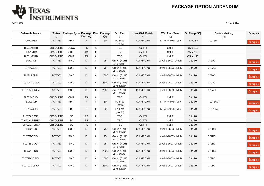
PACKAGE OPTION ADDENDUM
www.ti.com 7-Nov-2014
Addendum-Page 3
Orderable Device Status(1)
Package Type PackageDrawing
Pins PackageQty
Eco Plan(2)
Lead/Ball Finish(6)
MSL Peak Temp(3)
Op Temp (°C) Device Marking(4/5)
Samples
TL071IPE4 ACTIVE PDIP P 8 50 Pb-Free(RoHS)
CU NIPDAU N / A for Pkg Type -40 to 85 TL071IP
TL071MFKB OBSOLETE LCCC FK 20 TBD Call TI Call TI -55 to 125
TL071MJG OBSOLETE CDIP JG 8 TBD Call TI Call TI -55 to 125
TL071MJGB OBSOLETE CDIP JG 8 TBD Call TI Call TI -55 to 125
TL072ACD ACTIVE SOIC D 8 75 Green (RoHS& no Sb/Br)
CU NIPDAU Level-1-260C-UNLIM 0 to 70 072AC
TL072ACDE4 ACTIVE SOIC D 8 75 Green (RoHS& no Sb/Br)
CU NIPDAU Level-1-260C-UNLIM 0 to 70 072AC
TL072ACDR ACTIVE SOIC D 8 2500 Green (RoHS& no Sb/Br)
CU NIPDAU Level-1-260C-UNLIM 0 to 70 072AC
TL072ACDRE4 ACTIVE SOIC D 8 2500 Green (RoHS& no Sb/Br)
CU NIPDAU Level-1-260C-UNLIM 0 to 70 072AC
TL072ACDRG4 ACTIVE SOIC D 8 2500 Green (RoHS& no Sb/Br)
CU NIPDAU Level-1-260C-UNLIM 0 to 70 072AC
TL072ACJG OBSOLETE CDIP JG 8 TBD Call TI Call TI 0 to 70
TL072ACP ACTIVE PDIP P 8 50 Pb-Free(RoHS)
CU NIPDAU N / A for Pkg Type 0 to 70 TL072ACP
TL072ACPE4 ACTIVE PDIP P 8 50 Pb-Free(RoHS)
CU NIPDAU N / A for Pkg Type 0 to 70 TL072ACP
TL072ACPSR OBSOLETE SO PS 8 TBD Call TI Call TI 0 to 70
TL072ACPSRE4 OBSOLETE SO PS 8 TBD Call TI Call TI 0 to 70
TL072ACPSRG4 OBSOLETE SO PS 8 TBD Call TI Call TI 0 to 70
TL072BCD ACTIVE SOIC D 8 75 Green (RoHS& no Sb/Br)
CU NIPDAU Level-1-260C-UNLIM 0 to 70 072BC
TL072BCDE4 ACTIVE SOIC D 8 75 Green (RoHS& no Sb/Br)
CU NIPDAU Level-1-260C-UNLIM 0 to 70 072BC
TL072BCDG4 ACTIVE SOIC D 8 75 Green (RoHS& no Sb/Br)
CU NIPDAU Level-1-260C-UNLIM 0 to 70 072BC
TL072BCDR ACTIVE SOIC D 8 2500 Green (RoHS& no Sb/Br)
CU NIPDAU Level-1-260C-UNLIM 0 to 70 072BC
TL072BCDRE4 ACTIVE SOIC D 8 2500 Green (RoHS& no Sb/Br)
CU NIPDAU Level-1-260C-UNLIM 0 to 70 072BC
TL072BCDRG4 ACTIVE SOIC D 8 2500 Green (RoHS& no Sb/Br)
CU NIPDAU Level-1-260C-UNLIM 0 to 70 072BC
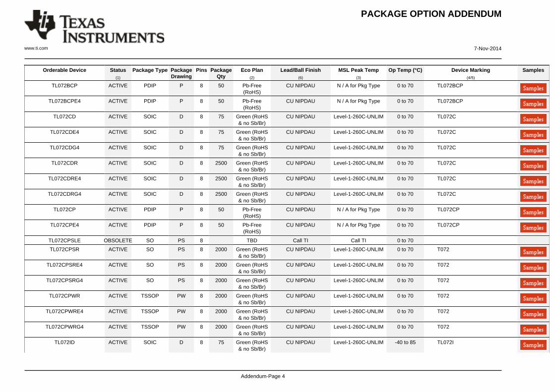
PACKAGE OPTION ADDENDUM
www.ti.com 7-Nov-2014
Addendum-Page 4
Orderable Device Status(1)
Package Type PackageDrawing
Pins PackageQty
Eco Plan(2)
Lead/Ball Finish(6)
MSL Peak Temp(3)
Op Temp (°C) Device Marking(4/5)
Samples
TL072BCP ACTIVE PDIP P 8 50 Pb-Free(RoHS)
CU NIPDAU N / A for Pkg Type 0 to 70 TL072BCP
TL072BCPE4 ACTIVE PDIP P 8 50 Pb-Free(RoHS)
CU NIPDAU N / A for Pkg Type 0 to 70 TL072BCP
TL072CD ACTIVE SOIC D 8 75 Green (RoHS& no Sb/Br)
CU NIPDAU Level-1-260C-UNLIM 0 to 70 TL072C
TL072CDE4 ACTIVE SOIC D 8 75 Green (RoHS& no Sb/Br)
CU NIPDAU Level-1-260C-UNLIM 0 to 70 TL072C
TL072CDG4 ACTIVE SOIC D 8 75 Green (RoHS& no Sb/Br)
CU NIPDAU Level-1-260C-UNLIM 0 to 70 TL072C
TL072CDR ACTIVE SOIC D 8 2500 Green (RoHS& no Sb/Br)
CU NIPDAU Level-1-260C-UNLIM 0 to 70 TL072C
TL072CDRE4 ACTIVE SOIC D 8 2500 Green (RoHS& no Sb/Br)
CU NIPDAU Level-1-260C-UNLIM 0 to 70 TL072C
TL072CDRG4 ACTIVE SOIC D 8 2500 Green (RoHS& no Sb/Br)
CU NIPDAU Level-1-260C-UNLIM 0 to 70 TL072C
TL072CP ACTIVE PDIP P 8 50 Pb-Free(RoHS)
CU NIPDAU N / A for Pkg Type 0 to 70 TL072CP
TL072CPE4 ACTIVE PDIP P 8 50 Pb-Free(RoHS)
CU NIPDAU N / A for Pkg Type 0 to 70 TL072CP
TL072CPSLE OBSOLETE SO PS 8 TBD Call TI Call TI 0 to 70
TL072CPSR ACTIVE SO PS 8 2000 Green (RoHS& no Sb/Br)
CU NIPDAU Level-1-260C-UNLIM 0 to 70 T072
TL072CPSRE4 ACTIVE SO PS 8 2000 Green (RoHS& no Sb/Br)
CU NIPDAU Level-1-260C-UNLIM 0 to 70 T072
TL072CPSRG4 ACTIVE SO PS 8 2000 Green (RoHS& no Sb/Br)
CU NIPDAU Level-1-260C-UNLIM 0 to 70 T072
TL072CPWR ACTIVE TSSOP PW 8 2000 Green (RoHS& no Sb/Br)
CU NIPDAU Level-1-260C-UNLIM 0 to 70 T072
TL072CPWRE4 ACTIVE TSSOP PW 8 2000 Green (RoHS& no Sb/Br)
CU NIPDAU Level-1-260C-UNLIM 0 to 70 T072
TL072CPWRG4 ACTIVE TSSOP PW 8 2000 Green (RoHS& no Sb/Br)
CU NIPDAU Level-1-260C-UNLIM 0 to 70 T072
TL072ID ACTIVE SOIC D 8 75 Green (RoHS& no Sb/Br)
CU NIPDAU Level-1-260C-UNLIM -40 to 85 TL072I
PACKAGE OPTION ADDENDUM
www.ti.com 7-Nov-2014
Addendum-Page 5
Orderable Device Status(1)
Package Type PackageDrawing
Pins PackageQty
Eco Plan(2)
Lead/Ball Finish(6)
MSL Peak Temp(3)
Op Temp (°C) Device Marking(4/5)
Samples
TL072IDE4 ACTIVE SOIC D 8 75 Green (RoHS& no Sb/Br)
CU NIPDAU Level-1-260C-UNLIM -40 to 85 TL072I
TL072IDG4 ACTIVE SOIC D 8 75 Green (RoHS& no Sb/Br)
CU NIPDAU Level-1-260C-UNLIM -40 to 85 TL072I
TL072IDR ACTIVE SOIC D 8 2500 Green (RoHS& no Sb/Br)
CU NIPDAU Level-1-260C-UNLIM -40 to 85 TL072I
TL072IDRE4 ACTIVE SOIC D 8 2500 Green (RoHS& no Sb/Br)
CU NIPDAU Level-1-260C-UNLIM -40 to 85 TL072I
TL072IDRG4 ACTIVE SOIC D 8 2500 Green (RoHS& no Sb/Br)
CU NIPDAU Level-1-260C-UNLIM -40 to 85 TL072I
TL072IP ACTIVE PDIP P 8 50 Pb-Free(RoHS)
CU NIPDAU N / A for Pkg Type -40 to 85 TL072IP
TL072IPE4 ACTIVE PDIP P 8 50 Pb-Free(RoHS)
CU NIPDAU N / A for Pkg Type -40 to 85 TL072IP
TL072MFKB ACTIVE LCCC FK 20 1 TBD POST-PLATE N / A for Pkg Type -55 to 125 81023052ATL072MFKB
TL072MJG ACTIVE CDIP JG 8 1 TBD A42 N / A for Pkg Type -55 to 125 TL072MJG
TL072MJGB ACTIVE CDIP JG 8 1 TBD A42 N / A for Pkg Type -55 to 125 8102305PATL072M
TL072MUB ACTIVE CFP U 10 1 TBD A42 N / A for Pkg Type -55 to 125 8102305HATL072M
TL074ACD ACTIVE SOIC D 14 50 Green (RoHS& no Sb/Br)
CU NIPDAU Level-1-260C-UNLIM 0 to 70 TL074AC
TL074ACDE4 ACTIVE SOIC D 14 50 Green (RoHS& no Sb/Br)
CU NIPDAU Level-1-260C-UNLIM 0 to 70 TL074AC
TL074ACDG4 ACTIVE SOIC D 14 50 Green (RoHS& no Sb/Br)
CU NIPDAU Level-1-260C-UNLIM 0 to 70 TL074AC
TL074ACDR ACTIVE SOIC D 14 2500 Green (RoHS& no Sb/Br)
CU NIPDAU Level-1-260C-UNLIM 0 to 70 TL074AC
TL074ACDRE4 ACTIVE SOIC D 14 2500 Green (RoHS& no Sb/Br)
CU NIPDAU Level-1-260C-UNLIM 0 to 70 TL074AC
TL074ACDRG4 ACTIVE SOIC D 14 2500 Green (RoHS& no Sb/Br)
CU NIPDAU Level-1-260C-UNLIM 0 to 70 TL074AC
TL074ACJ OBSOLETE CDIP J 14 TBD Call TI Call TI 0 to 70

PACKAGE OPTION ADDENDUM
www.ti.com 7-Nov-2014
Addendum-Page 6
Orderable Device Status(1)
Package Type PackageDrawing
Pins PackageQty
Eco Plan(2)
Lead/Ball Finish(6)
MSL Peak Temp(3)
Op Temp (°C) Device Marking(4/5)
Samples
TL074ACN ACTIVE PDIP N 14 25 Pb-Free(RoHS)
CU NIPDAU N / A for Pkg Type 0 to 70 TL074ACN
TL074ACNE4 ACTIVE PDIP N 14 25 Pb-Free(RoHS)
CU NIPDAU N / A for Pkg Type 0 to 70 TL074ACN
TL074ACNSR ACTIVE SO NS 14 2000 Green (RoHS& no Sb/Br)
CU NIPDAU Level-1-260C-UNLIM 0 to 70 TL074A
TL074BCD ACTIVE SOIC D 14 50 Green (RoHS& no Sb/Br)
CU NIPDAU Level-1-260C-UNLIM 0 to 70 TL074BC
TL074BCDE4 ACTIVE SOIC D 14 50 Green (RoHS& no Sb/Br)
CU NIPDAU Level-1-260C-UNLIM 0 to 70 TL074BC
TL074BCDG4 ACTIVE SOIC D 14 50 Green (RoHS& no Sb/Br)
CU NIPDAU Level-1-260C-UNLIM 0 to 70 TL074BC
TL074BCDR ACTIVE SOIC D 14 2500 Green (RoHS& no Sb/Br)
CU NIPDAU Level-1-260C-UNLIM 0 to 70 TL074BC
TL074BCDRE4 ACTIVE SOIC D 14 2500 Green (RoHS& no Sb/Br)
CU NIPDAU Level-1-260C-UNLIM 0 to 70 TL074BC
TL074BCDRG4 ACTIVE SOIC D 14 2500 Green (RoHS& no Sb/Br)
CU NIPDAU Level-1-260C-UNLIM 0 to 70 TL074BC
TL074BCN ACTIVE PDIP N 14 25 Pb-Free(RoHS)
CU NIPDAU N / A for Pkg Type 0 to 70 TL074BCN
TL074BCNE4 ACTIVE PDIP N 14 25 Pb-Free(RoHS)
CU NIPDAU N / A for Pkg Type 0 to 70 TL074BCN
TL074CD ACTIVE SOIC D 14 50 Green (RoHS& no Sb/Br)
CU NIPDAU Level-1-260C-UNLIM 0 to 70 TL074C
TL074CDE4 ACTIVE SOIC D 14 50 Green (RoHS& no Sb/Br)
CU NIPDAU Level-1-260C-UNLIM 0 to 70 TL074C
TL074CDG4 ACTIVE SOIC D 14 50 Green (RoHS& no Sb/Br)
CU NIPDAU Level-1-260C-UNLIM 0 to 70 TL074C
TL074CDR ACTIVE SOIC D 14 2500 Green (RoHS& no Sb/Br)
CU NIPDAU | CU SN Level-1-260C-UNLIM 0 to 70 TL074C
TL074CDRE4 ACTIVE SOIC D 14 2500 Green (RoHS& no Sb/Br)
CU NIPDAU Level-1-260C-UNLIM 0 to 70 TL074C
TL074CDRG4 ACTIVE SOIC D 14 2500 Green (RoHS& no Sb/Br)
CU NIPDAU Level-1-260C-UNLIM 0 to 70 TL074C
TL074CN ACTIVE PDIP N 14 25 Pb-Free(RoHS)
CU NIPDAU N / A for Pkg Type 0 to 70 TL074CN

PACKAGE OPTION ADDENDUM
www.ti.com 7-Nov-2014
Addendum-Page 7
Orderable Device Status(1)
Package Type PackageDrawing
Pins PackageQty
Eco Plan(2)
Lead/Ball Finish(6)
MSL Peak Temp(3)
Op Temp (°C) Device Marking(4/5)
Samples
TL074CNE4 ACTIVE PDIP N 14 25 Pb-Free(RoHS)
CU NIPDAU N / A for Pkg Type 0 to 70 TL074CN
TL074CNSR ACTIVE SO NS 14 2000 Green (RoHS& no Sb/Br)
CU NIPDAU Level-1-260C-UNLIM 0 to 70 TL074
TL074CNSRG4 ACTIVE SO NS 14 2000 Green (RoHS& no Sb/Br)
CU NIPDAU Level-1-260C-UNLIM 0 to 70 TL074
TL074CPW ACTIVE TSSOP PW 14 90 Green (RoHS& no Sb/Br)
CU NIPDAU Level-1-260C-UNLIM 0 to 70 T074
TL074CPWG4 ACTIVE TSSOP PW 14 90 Green (RoHS& no Sb/Br)
CU NIPDAU Level-1-260C-UNLIM 0 to 70 T074
TL074CPWLE OBSOLETE TSSOP PW 14 TBD Call TI Call TI 0 to 70
TL074CPWR ACTIVE TSSOP PW 14 2000 Green (RoHS& no Sb/Br)
CU NIPDAU Level-1-260C-UNLIM 0 to 70 T074
TL074CPWRE4 ACTIVE TSSOP PW 14 2000 Green (RoHS& no Sb/Br)
CU NIPDAU Level-1-260C-UNLIM 0 to 70 T074
TL074CPWRG4 ACTIVE TSSOP PW 14 2000 Green (RoHS& no Sb/Br)
CU NIPDAU Level-1-260C-UNLIM 0 to 70 T074
TL074ID ACTIVE SOIC D 14 50 Green (RoHS& no Sb/Br)
CU NIPDAU Level-1-260C-UNLIM -40 to 85 TL074I
TL074IDE4 ACTIVE SOIC D 14 50 Green (RoHS& no Sb/Br)
CU NIPDAU Level-1-260C-UNLIM -40 to 85 TL074I
TL074IDG4 ACTIVE SOIC D 14 50 Green (RoHS& no Sb/Br)
CU NIPDAU Level-1-260C-UNLIM -40 to 85 TL074I
TL074IDR ACTIVE SOIC D 14 2500 Green (RoHS& no Sb/Br)
CU NIPDAU Level-1-260C-UNLIM -40 to 85 TL074I
TL074IDRE4 ACTIVE SOIC D 14 2500 Green (RoHS& no Sb/Br)
CU NIPDAU Level-1-260C-UNLIM -40 to 85 TL074I
TL074IDRG4 ACTIVE SOIC D 14 2500 Green (RoHS& no Sb/Br)
CU NIPDAU Level-1-260C-UNLIM -40 to 85 TL074I
TL074IJ OBSOLETE CDIP J 14 TBD Call TI Call TI -40 to 85
TL074IN ACTIVE PDIP N 14 25 Pb-Free(RoHS)
CU NIPDAU N / A for Pkg Type -40 to 85 TL074IN
TL074INE4 ACTIVE PDIP N 14 25 Pb-Free(RoHS)
CU NIPDAU N / A for Pkg Type -40 to 85 TL074IN
TL074MFK ACTIVE LCCC FK 20 1 TBD POST-PLATE N / A for Pkg Type -55 to 125 TL074MFK
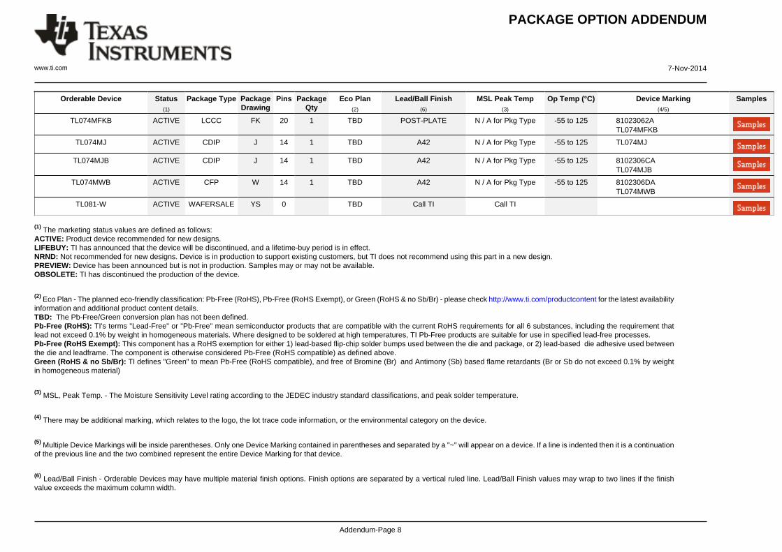
PACKAGE OPTION ADDENDUM
www.ti.com 7-Nov-2014
Addendum-Page 8
Orderable Device Status(1)
Package Type PackageDrawing
Pins PackageQty
Eco Plan(2)
Lead/Ball Finish(6)
MSL Peak Temp(3)
Op Temp (°C) Device Marking(4/5)
Samples
TL074MFKB ACTIVE LCCC FK 20 1 TBD POST-PLATE N / A for Pkg Type -55 to 125 81023062ATL074MFKB
TL074MJ ACTIVE CDIP J 14 1 TBD A42 N / A for Pkg Type -55 to 125 TL074MJ
TL074MJB ACTIVE CDIP J 14 1 TBD A42 N / A for Pkg Type -55 to 125 8102306CATL074MJB
TL074MWB ACTIVE CFP W 14 1 TBD A42 N / A for Pkg Type -55 to 125 8102306DATL074MWB
TL081-W ACTIVE WAFERSALE YS 0 TBD Call TI Call TI
(1) The marketing status values are defined as follows:ACTIVE: Product device recommended for new designs.LIFEBUY: TI has announced that the device will be discontinued, and a lifetime-buy period is in effect.NRND: Not recommended for new designs. Device is in production to support existing customers, but TI does not recommend using this part in a new design.PREVIEW: Device has been announced but is not in production. Samples may or may not be available.OBSOLETE: TI has discontinued the production of the device.
(2) Eco Plan - The planned eco-friendly classification: Pb-Free (RoHS), Pb-Free (RoHS Exempt), or Green (RoHS & no Sb/Br) - please check http://www.ti.com/productcontent for the latest availabilityinformation and additional product content details.TBD: The Pb-Free/Green conversion plan has not been defined.Pb-Free (RoHS): TI's terms "Lead-Free" or "Pb-Free" mean semiconductor products that are compatible with the current RoHS requirements for all 6 substances, including the requirement thatlead not exceed 0.1% by weight in homogeneous materials. Where designed to be soldered at high temperatures, TI Pb-Free products are suitable for use in specified lead-free processes.Pb-Free (RoHS Exempt): This component has a RoHS exemption for either 1) lead-based flip-chip solder bumps used between the die and package, or 2) lead-based die adhesive used betweenthe die and leadframe. The component is otherwise considered Pb-Free (RoHS compatible) as defined above.Green (RoHS & no Sb/Br): TI defines "Green" to mean Pb-Free (RoHS compatible), and free of Bromine (Br) and Antimony (Sb) based flame retardants (Br or Sb do not exceed 0.1% by weightin homogeneous material)
(3) MSL, Peak Temp. - The Moisture Sensitivity Level rating according to the JEDEC industry standard classifications, and peak solder temperature.
(4) There may be additional marking, which relates to the logo, the lot trace code information, or the environmental category on the device.
(5) Multiple Device Markings will be inside parentheses. Only one Device Marking contained in parentheses and separated by a "~" will appear on a device. If a line is indented then it is a continuationof the previous line and the two combined represent the entire Device Marking for that device.
(6) Lead/Ball Finish - Orderable Devices may have multiple material finish options. Finish options are separated by a vertical ruled line. Lead/Ball Finish values may wrap to two lines if the finishvalue exceeds the maximum column width.
PACKAGE OPTION ADDENDUM
www.ti.com 7-Nov-2014
Addendum-Page 9
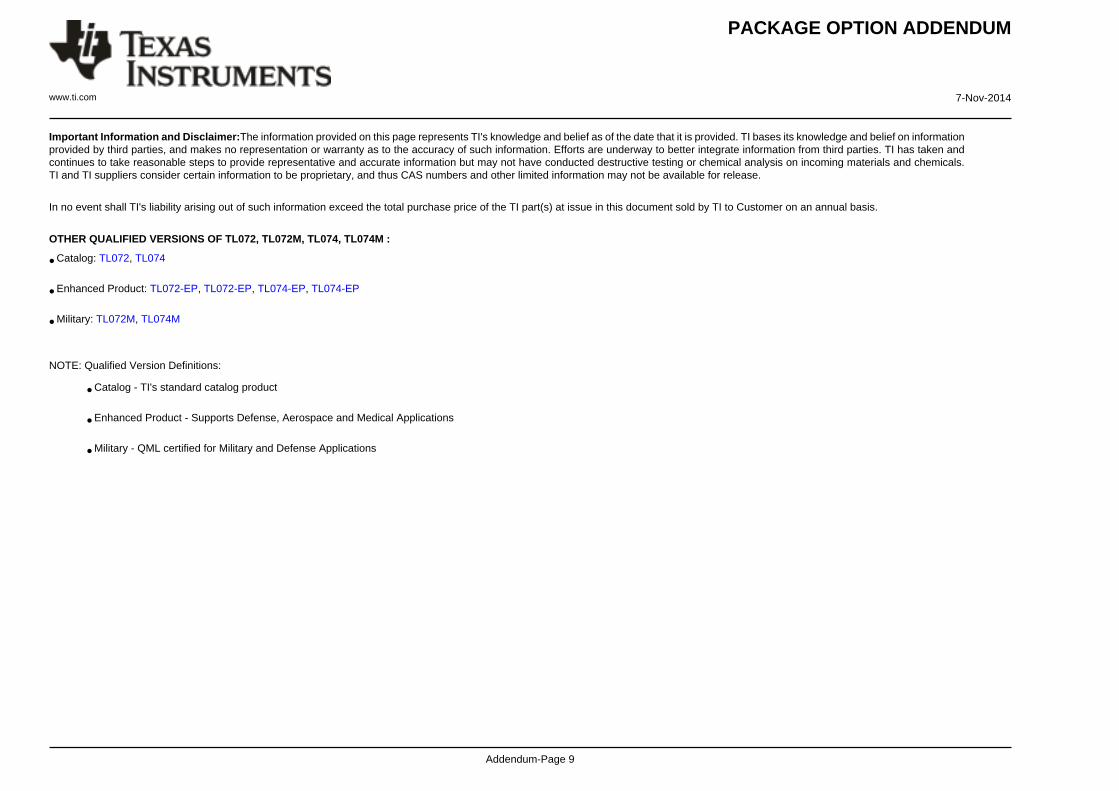
Important Information and Disclaimer:The information provided on this page represents TI's knowledge and belief as of the date that it is provided. TI bases its knowledge and belief on informationprovided by third parties, and makes no representation or warranty as to the accuracy of such information. Efforts are underway to better integrate information from third parties. TI has taken andcontinues to take reasonable steps to provide representative and accurate information but may not have conducted destructive testing or chemical analysis on incoming materials and chemicals.TI and TI suppliers consider certain information to be proprietary, and thus CAS numbers and other limited information may not be available for release.
In no event shall TI's liability arising out of such information exceed the total purchase price of the TI part(s) at issue in this document sold by TI to Customer on an annual basis.
OTHER QUALIFIED VERSIONS OF TL072, TL072M, TL074, TL074M :
• Catalog: TL072, TL074
• Enhanced Product: TL072-EP, TL072-EP, TL074-EP, TL074-EP
• Military: TL072M, TL074M
NOTE: Qualified Version Definitions:
• Catalog - TI's standard catalog product
• Enhanced Product - Supports Defense, Aerospace and Medical Applications
• Military - QML certified for Military and Defense Applications
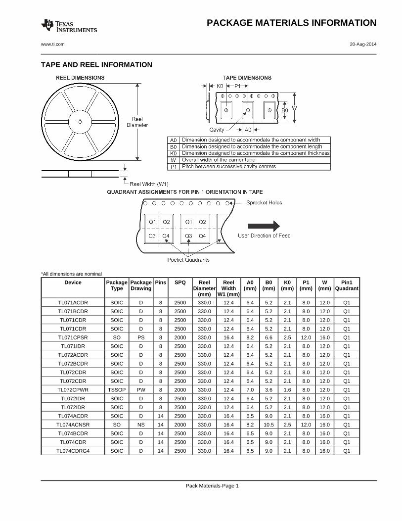
TAPE AND REEL INFORMATION
*All dimensions are nominal
Device PackageType
PackageDrawing
Pins SPQ ReelDiameter
(mm)
ReelWidth
W1 (mm)
A0(mm)
B0(mm)
K0(mm)
P1(mm)
W(mm)
Pin1Quadrant
TL071ACDR SOIC D 8 2500 330.0 12.4 6.4 5.2 2.1 8.0 12.0 Q1
TL071BCDR SOIC D 8 2500 330.0 12.4 6.4 5.2 2.1 8.0 12.0 Q1
TL071CDR SOIC D 8 2500 330.0 12.4 6.4 5.2 2.1 8.0 12.0 Q1
TL071CDR SOIC D 8 2500 330.0 12.4 6.4 5.2 2.1 8.0 12.0 Q1
TL071CPSR SO PS 8 2000 330.0 16.4 8.2 6.6 2.5 12.0 16.0 Q1
TL071IDR SOIC D 8 2500 330.0 12.4 6.4 5.2 2.1 8.0 12.0 Q1
TL072ACDR SOIC D 8 2500 330.0 12.4 6.4 5.2 2.1 8.0 12.0 Q1
TL072BCDR SOIC D 8 2500 330.0 12.4 6.4 5.2 2.1 8.0 12.0 Q1
TL072CDR SOIC D 8 2500 330.0 12.4 6.4 5.2 2.1 8.0 12.0 Q1
TL072CDR SOIC D 8 2500 330.0 12.4 6.4 5.2 2.1 8.0 12.0 Q1
TL072CPWR TSSOP PW 8 2000 330.0 12.4 7.0 3.6 1.6 8.0 12.0 Q1
TL072IDR SOIC D 8 2500 330.0 12.4 6.4 5.2 2.1 8.0 12.0 Q1
TL072IDR SOIC D 8 2500 330.0 12.4 6.4 5.2 2.1 8.0 12.0 Q1
TL074ACDR SOIC D 14 2500 330.0 16.4 6.5 9.0 2.1 8.0 16.0 Q1
TL074ACNSR SO NS 14 2000 330.0 16.4 8.2 10.5 2.5 12.0 16.0 Q1
TL074BCDR SOIC D 14 2500 330.0 16.4 6.5 9.0 2.1 8.0 16.0 Q1
TL074CDR SOIC D 14 2500 330.0 16.4 6.5 9.0 2.1 8.0 16.0 Q1
TL074CDRG4 SOIC D 14 2500 330.0 16.4 6.5 9.0 2.1 8.0 16.0 Q1
PACKAGE MATERIALS INFORMATION
www.ti.com 20-Aug-2014
Pack Materials-Page 1
Device PackageType
PackageDrawing
Pins SPQ ReelDiameter
(mm)
ReelWidth
W1 (mm)
A0(mm)
B0(mm)
K0(mm)
P1(mm)
W(mm)
Pin1Quadrant
TL074CPWR TSSOP PW 14 2000 330.0 12.4 6.9 5.6 1.6 8.0 12.0 Q1
TL074IDR SOIC D 14 2500 330.0 16.4 6.5 9.0 2.1 8.0 16.0 Q1
*All dimensions are nominal
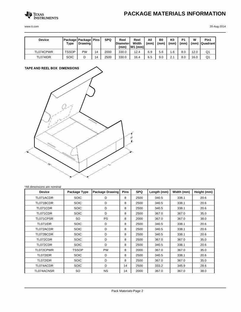
Device Package Type Package Drawing Pins SPQ Length (mm) Width (mm) Height (mm)
TL071ACDR SOIC D 8 2500 340.5 338.1 20.6
TL071BCDR SOIC D 8 2500 340.5 338.1 20.6
TL071CDR SOIC D 8 2500 340.5 338.1 20.6
TL071CDR SOIC D 8 2500 367.0 367.0 35.0
TL071CPSR SO PS 8 2000 367.0 367.0 38.0
TL071IDR SOIC D 8 2500 340.5 338.1 20.6
TL072ACDR SOIC D 8 2500 340.5 338.1 20.6
TL072BCDR SOIC D 8 2500 340.5 338.1 20.6
TL072CDR SOIC D 8 2500 367.0 367.0 35.0
TL072CDR SOIC D 8 2500 340.5 338.1 20.6
TL072CPWR TSSOP PW 8 2000 367.0 367.0 35.0
TL072IDR SOIC D 8 2500 340.5 338.1 20.6
TL072IDR SOIC D 8 2500 367.0 367.0 35.0
TL074ACDR SOIC D 14 2500 333.2 345.9 28.6
TL074ACNSR SO NS 14 2000 367.0 367.0 38.0
PACKAGE MATERIALS INFORMATION
www.ti.com 20-Aug-2014
Pack Materials-Page 2
Device Package Type Package Drawing Pins SPQ Length (mm) Width (mm) Height (mm)
TL074BCDR SOIC D 14 2500 333.2 345.9 28.6
TL074CDR SOIC D 14 2500 333.2 345.9 28.6
TL074CDRG4 SOIC D 14 2500 333.2 345.9 28.6
TL074CPWR TSSOP PW 14 2000 367.0 367.0 35.0
TL074IDR SOIC D 14 2500 333.2 345.9 28.6
PACKAGE MATERIALS INFORMATION
www.ti.com 20-Aug-2014
Pack Materials-Page 3
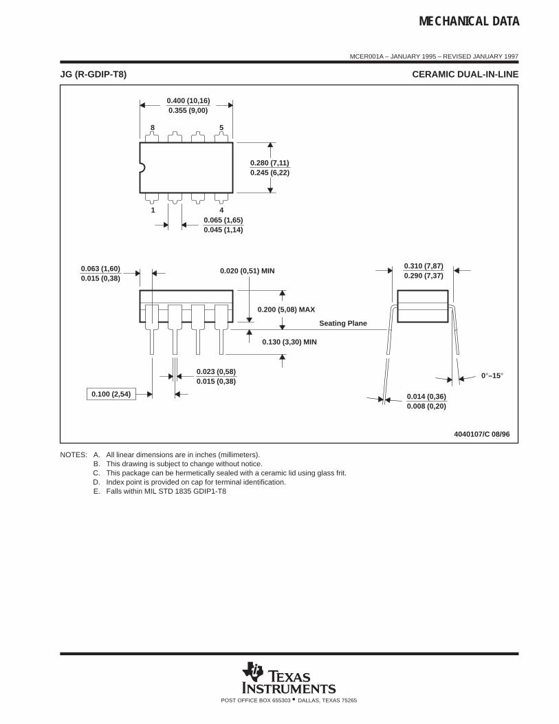
MECHANICAL DATA
MCER001A – JANUARY 1995 – REVISED JANUARY 1997
POST OFFICE BOX 655303 • DALLAS, TEXAS 75265
JG (R-GDIP-T8) CERAMIC DUAL-IN-LINE
0.310 (7,87)0.290 (7,37)
0.014 (0,36)0.008 (0,20)
Seating Plane
4040107/C 08/96
5
40.065 (1,65)0.045 (1,14)
8
1
0.020 (0,51) MIN
0.400 (10,16)0.355 (9,00)
0.015 (0,38)0.023 (0,58)
0.063 (1,60)0.015 (0,38)
0.200 (5,08) MAX
0.130 (3,30) MIN
0.245 (6,22)0.280 (7,11)
0.100 (2,54)
0°–15°
NOTES: A. All linear dimensions are in inches (millimeters).B. This drawing is subject to change without notice.C. This package can be hermetically sealed with a ceramic lid using glass frit.D. Index point is provided on cap for terminal identification.E. Falls within MIL STD 1835 GDIP1-T8

IMPORTANT NOTICETexas Instruments Incorporated and its subsidiaries (TI) reserve the right to make corrections, enhancements, improvements and otherchanges to its semiconductor products and services per JESD46, latest issue, and to discontinue any product or service per JESD48, latestissue. Buyers should obtain the latest relevant information before placing orders and should verify that such information is current andcomplete. All semiconductor products (also referred to herein as “components”) are sold subject to TI’s terms and conditions of salesupplied at the time of order acknowledgment.TI warrants performance of its components to the specifications applicable at the time of sale, in accordance with the warranty in TI’s termsand conditions of sale of semiconductor products. Testing and other quality control techniques are used to the extent TI deems necessaryto support this warranty. Except where mandated by applicable law, testing of all parameters of each component is not necessarilyperformed.TI assumes no liability for applications assistance or the design of Buyers’ products. Buyers are responsible for their products andapplications using TI components. To minimize the risks associated with Buyers’ products and applications, Buyers should provideadequate design and operating safeguards.TI does not warrant or represent that any license, either express or implied, is granted under any patent right, copyright, mask work right, orother intellectual property right relating to any combination, machine, or process in which TI components or services are used. Informationpublished by TI regarding third-party products or services does not constitute a license to use such products or services or a warranty orendorsement thereof. Use of such information may require a license from a third party under the patents or other intellectual property of thethird party, or a license from TI under the patents or other intellectual property of TI.Reproduction of significant portions of TI information in TI data books or data sheets is permissible only if reproduction is without alterationand is accompanied by all associated warranties, conditions, limitations, and notices. TI is not responsible or liable for such altereddocumentation. Information of third parties may be subject to additional restrictions.Resale of TI components or services with statements different from or beyond the parameters stated by TI for that component or servicevoids all express and any implied warranties for the associated TI component or service and is an unfair and deceptive business practice.TI is not responsible or liable for any such statements.Buyer acknowledges and agrees that it is solely responsible for compliance with all legal, regulatory and safety-related requirementsconcerning its products, and any use of TI components in its applications, notwithstanding any applications-related information or supportthat may be provided by TI. Buyer represents and agrees that it has all the necessary expertise to create and implement safeguards whichanticipate dangerous consequences of failures, monitor failures and their consequences, lessen the likelihood of failures that might causeharm and take appropriate remedial actions. Buyer will fully indemnify TI and its representatives against any damages arising out of the useof any TI components in safety-critical applications.In some cases, TI components may be promoted specifically to facilitate safety-related applications. With such components, TI’s goal is tohelp enable customers to design and create their own end-product solutions that meet applicable functional safety standards andrequirements. Nonetheless, such components are subject to these terms.No TI components are authorized for use in FDA Class III (or similar life-critical medical equipment) unless authorized officers of the partieshave executed a special agreement specifically governing such use.Only those TI components which TI has specifically designated as military grade or “enhanced plastic” are designed and intended for use inmilitary/aerospace applications or environments. Buyer acknowledges and agrees that any military or aerospace use of TI componentswhich have not been so designated is solely at the Buyer's risk, and that Buyer is solely responsible for compliance with all legal andregulatory requirements in connection with such use.TI has specifically designated certain components as meeting ISO/TS16949 requirements, mainly for automotive use. In any case of use ofnon-designated products, TI will not be responsible for any failure to meet ISO/TS16949.Products ApplicationsAudio www.ti.com/audio Automotive and Transportation www.ti.com/automotiveAmplifiers amplifier.ti.com Communications and Telecom www.ti.com/communicationsData Converters dataconverter.ti.com Computers and Peripherals www.ti.com/computersDLP® Products www.dlp.com Consumer Electronics www.ti.com/consumer-appsDSP dsp.ti.com Energy and Lighting www.ti.com/energyClocks and Timers www.ti.com/clocks Industrial www.ti.com/industrialInterface interface.ti.com Medical www.ti.com/medicalLogic logic.ti.com Security www.ti.com/securityPower Mgmt power.ti.com Space, Avionics and Defense www.ti.com/space-avionics-defenseMicrocontrollers microcontroller.ti.com Video and Imaging www.ti.com/videoRFID www.ti-rfid.comOMAP Applications Processors www.ti.com/omap TI E2E Community e2e.ti.comWireless Connectivity www.ti.com/wirelessconnectivity
Mailing Address: Texas Instruments, Post Office Box 655303, Dallas, Texas 75265Copyright © 2014, Texas Instruments Incorporated