size reduction research for the universal initiator … reduction research for the universal...
TRANSCRIPT

Size Reduction Research for the Universal
Initiator CY2001 Report
by William Lawler and Dan Judy
ARL-MR-593 June 2004 Approved for public release; distribution unlimited.

NOTICES
Disclaimers The findings in this report are not to be construed as an official Department of the Army position unless so designated by other authorized documents. Citation of manufacturer’s or trade names does not constitute an official endorsement or approval of the use thereof. Destroy this report when it is no longer needed. Do not return it to the originator.

Army Research Laboratory Adelphi, MD 20783-1197
ARL-MR-593 June 2004
Size Reduction Research for the Universal Initiator CT2001 Report
William Lawler and Dan Judy
Sensors and Electron Devices Directorate, ARL Approved for public release; distribution unlimited.

ii
REPORT DOCUMENTATION PAGE Form Approved OMB No. 0704-0188
Public reporting burden for this collection of information is estimated to average 1 hour per response, including the time for reviewing instructions, searching existing data sources, gathering and maintaining the data needed, and completing and reviewing the collection information. Send comments regarding this burden estimate or any other aspect of this collection of information, including suggestions for reducing the burden, to Department of Defense, Washington Headquarters Services, Directorate for Information Operations and Reports (0704-0188), 1215 Jefferson Davis Highway, Suite 1204, Arlington, VA 22202-4302. Respondents should be aware that notwithstanding any other provision of law, no person shall be subject to any penalty for failing to comply with a collection of information if it does not display a currently valid OMB control number. PLEASE DO NOT RETURN YOUR FORM TO THE ABOVE ADDRESS. 1. REPORT DATE (DD-MM-YYYY)
June 2004 2. REPORT TYPE
Final 3. DATES COVERED (From - To)
January to December 2001 5a. CONTRACT NUMBER
5b. GRANT NUMBER
4. TITLE AND SUBTITLE
Size Reduction Research for the Universal Initiator CY2001 Report
5c. PROGRAM ELEMENT NUMBER
5d. PROJECT NUMBER
1NR8RR 5e. TASK NUMBER
6. AUTHOR(S)
William Lawler and Dan Judy
5f. WORK UNIT NUMBER
7. PERFORMING ORGANIZATION NAME(S) AND ADDRESS(ES)
U.S. Army Research Laboratory Attn: AMSRL-SE-RE 2800 Powder Mill Road Adelphi, MD 20783-1197
8. PERFORMING ORGANIZATION REPORT NUMBER
ARL-MR-593
10. SPONSOR/MONITOR'S ACRONYM(S)
9. SPONSORING/MONITORING AGENCY NAME(S) AND ADDRESS(ES)
U.S. Army Research Laboratory 2800 Powder Mill Road Adelphi, MD 20783-1197
11. SPONSOR/MONITOR'S REPORT NUMBER(S)
12. DISTRIBUTION/AVAILABILITY STATEMENT
Approved for public release; distribution unlimited.
13. SUPPLEMENTARY NOTES
14. ABSTRACT
We describe two aspects of miniaturization research for the proposed universal initiator (UI) system. The UI would combine functionality of the remote activation munitions system (RAMS) and the sympathetic detonation (SYDET) system. First, we discuss the results of a market survey of candidate display devices for UI, where we conclude that organic light emitting diode device technology is most appropriate. We also discuss twisted nematic liquid crystal diode device technology which is used in RAMS and SYDET. Second, we discuss possible size reduction in the quadrature detector of the radio frequency receiver used in the RAMS system, with emphasis on new parts and technologies. We show results of tests performed on a ceramic resonator that would allow significant size reduction in the receiver, and conclude that use of the ceramic device will result in an unacceptable loss in sensitivity of the receiver. The work was performed at the U.S. Army Research Laboratory in calendar year 2001.
15. SUBJECT TERMS
Universal initiator, RF receiver, LCD, OLED, display, fuze
16. SECURITY CLASSIFICATION OF: 19a. NAME OF RESPONSIBLE PERSON William Lawler
a. REPORT UNCLASSIFIED
b. ABSTRACT UNCLASSIFIED
c. THIS PAGE UNCLASSIFIED
17. LIMITATION OF ABSTRACT
UL
18. NUMBER OF PAGES
26 19b. TELEPHONE NUMBER (Include area code)
(301) 394-2460 Standard Form 298 (Rev. 8/98) Prescribed by ANSI Std. Z39.18

iii
Contents
List of Figures iv
1. Introduction 1
2. UI Display 1 2.1 TN LCD...........................................................................................................................1
2.2 OLED ..............................................................................................................................3
2.3 Graphic LCD Displays ....................................................................................................6
2.4 Display Summary ............................................................................................................8
3. RF Receiver Size Reduction Background 9 3.1 Experiment ....................................................................................................................10
3.2 Results ...........................................................................................................................10
3.3 RF Experiment Conclusions..........................................................................................13
4. CY2001 Research Summary 14
Appendix A. UI TN LCD Flow Chart 15
Appendix B. Organic Light Emitting Diode (OLED) 17
Distribution 21

iv
List of Figures
Figure 1. Candidate UI LCD format for direct drive segmented-TN LCD. (a) Possible layout and (b) schematic form of the segmented direct-drive TN/LCD. The glass dimensions are ~0.7 × 5 in. Characters are ~100 mil high. Segmented composition of characters is shown in (c)–(f).....................................................................................................2
Figure 2. (a) Proposed UI LCD display format and (b) SYDET display in approximate footprints. The minimum size UI display measures ~0.7 × 0.5 in, while the SYDET display is ~1.8 × 1.3 in. For ballpark comparison, using today’s design rules, the SYDET display would occupy 4 times the volume of this UI display...................................................3
Figure 3. Setup for observing the OLED SVGA display at different temperatures .......................5 Figure 4. Images of the SVGA OLED display output at temperatures of (a) –25 °F, (b) room
temperature, and (c) 140 °F. A CCD camera was placed in the temperature chamber with the display. A framegrabber was used to record the CCD output. The CCD camera was not calibrated or compensated for temperature changes. We did not attempt to quantify the CCD temperature dependence from that of the OLED. The experiment simply verifies that the OLED functions satisfactorily over the range –25–140 °F. The waviness in the horizontal and vertical lines is software-induced after image acquisition.................................5
Figure 5. Total forecast market value for OLED and LCD mobile displays with 1 in ≤ diagonal dimension ≥ 2 in. Market will be dominated by LCD displays, which are not expected to operate satisfactorily at low temperatures. Data from Stanford Resources...........7
Figure 6. Forecast of market value of OLED displays with 1 in ≤ diagonal dimension ≥ 2 in, active and passive matrix devices. Forecast shows, for example, a $220 million market for monochrome OLEDs of this size in 2004. Data from Stanford Resources ............7
Figure 7. Forecast of market value of OLED displays of all formats. Forecast component values in $ millions. Data from Stanford Resources.................................................................8
Figure 8. RF Block Diagram for (a) RAMS B and (b) experimental configuration using ceramic resonator at 455 kHz ..................................................................................................10
Figure 9. Block diagram of the experimental setup......................................................................11 Figure 10. Plot of mean frequency vs. input signal power for different temperatures, board 1
(air coil)....................................................................................................................................11 Figure 11. Plot of mean output frequency vs. input signal power for different temperatures,
board 2 (iron powder core) ......................................................................................................12 Figure 12. Plot of mean output frequency vs. input signal power for different temperatures,
board 3 (ceramic resonator) .....................................................................................................13

1
1. Introduction
The Calendar Year (CY) 2001 Universal Initiator (UI) miniaturization research tasks are as follows: (1) to research display technologies and conduct a market survey, and (2) size reduction in the quadrature detector of the radio frequency (RF) receiver with emphasis on new parts and technologies.
2. UI Display
A visual display is needed as the output device of the UI user interface. Most importantly, the display must have the capacity to annunciate “sufficient” data and cues to the user programming the UI. Additionally, it should be inexpensive, small in size and weight, environmentally rugged, dissipate little power, and must be compatible with standard night vision goggles. From the market/technology survey, two display technologies appear to be most appropriate for UI, twisted nematic (TN) liquid crystal diode (LCD), and organic light emitting diode (OLED).
2.1 TN LCD
Segmented TN LCDs satisfy most of the requirements previously listed. Segmented TN LCDs are simple, inexpensive, can operate over the required temperature range when driven with the direct drive method, and dissipate extremely low power. However, segmented LCDs have poor information density (information displayed per unit area of the display). A TN LCD is currently used for the sympathetic detonation (SYDET) display.
During the CY2000 work, we presented a preliminary design for a TN LCD considered to be the minimum size LCD display that may enunciate “adequate” data to the user for the anticipated UI programming tasks. This display, slightly modified in 2001, is composed of six segmented alpha-numeric characters (figure 1). Characters are ~100 mil high. The device would have 48 signal pins and 4 backplane pins for a total of 52. The glass dimensions would be ~0.7 × 0.5 in. A frame for mechanical support and electrical connectivity would increase the dimensions by ~0.2 in per side, yielding a module size of ~0.9 × 0.7 in. We devised a programming method that uses the six characters along with three Hall switches from SYDET for user input/output. Along with this, we developed a computer software emulation program (enclosed) to enable prospective users to experience how the interface would function. The emulation program, based on SYDET programming logic, leads the user through one particular path (the most complicated one) of the SYDET logic tree. The flow diagram of the emulation program appears in appendix A. For reference, we also enclose the emulation program for the SYDET display.

2
Figure 1. Candidate UI LCD format for direct drive segmented-TN LCD. (a) Possible layout and (b) schematic form of the segmented direct-drive TN/LCD. The glass dimensions are ~0.7 × 5 in. Characters are ~100 mil high. Segmented composition of characters is shown in (c)–(f).
Figure 2 shows the SYDET and proposed UI displays side by side for rough comparison. Using today’s design rules for convenience, the SYDET display is about twice the size of the proposed UI display in each dimension and about 4 times its volume. The volume of complete modules is estimated at ~0.2 in3 for the UI and 0.8 in3 for the SYDET. The UI display has 52 pin positions while the SYDET display has 104. For the regime of information content appropriate to this discussion, each linear dimension segmented LCD display increases approximately linearly with the number of segments. Another doubling of the number of segments would result in a display ~4 times the volume of SYDET or ~3.2 in3. Along with the LCD module size, the volume of the LCD driver circuits increases with the number of segments. The resources required by the driver chips are not insignificant in pin count, which translates into board area. The SYDET display requires three drive chips.
Displays made with the segmented TN LCD technology would be custom designed and manufactured in a standard process. For example, the SYDET displays have ~$10k nonrecurring engineering (NRE) and cost ~$15/unit in small quantities for LCD glass only (no drivers or
2 3 4Characters
8 segments
Character
5 6 segments
6Character
7 segments
Character
1 11 segments
1 2 3 4
5 6
a) b)
c)
e) f)
d)

3
Figure 2. (a) Proposed UI LCD display format and (b) SYDET display in approximate footprints. The minimum size UI display measures ~0.7 × 0.5 in, while the SYDET display is ~1.8 × 1.3 in. For ballpark comparison, using today’s design rules, the SYDET display would occupy 4 times the volume of this UI display.
fixtures). This technology is expected to be available through 2007; however, finding U.S. manufacturers willing to deal with small quantities may be problematic.
Many consumer applications use time-multiplexed TN LCDs. These passive-matrix devices are available in many formats: 1 (row) × 16 characters (of 5 × 7 dots each), 2 × 16, etc. The time multiplexing enables a small number of drivers to operate a large number of segments and keeps simple the driver circuits for a relatively complex character or rudimentary graphics display. There are a large number of commercially available modules of varying formats that would satisfy UI informational requirements. However, these multiplexed displays do not work adequately at low temperature. The TN LCDs must be driven directly (one drive channel per segment) in order to perform well at low temperature.
2.2 OLED
An emerging technology, OLEDs are made by building planar layers of organic materials that emit light through recombination of injected electrons and holes in a manner similar to discrete LEDs. In most other ways, OLEDs are different from discrete LEDs. The pitch of emitters in an OLED display is determined by the pitch of the drive circuits and can be as small as 10-12 µm, enabling high-resolution graphics as well as coarser dot-matrix displays, depending on the pitch of the drivers or passive address matrix. The manufacturing of OLEDs will be dominated by companies on the Pacific rim, where the devices are called organic electroluminescent (OEL) displays.
OLEDs are current devices (LCDs are voltage devices), and can be driven by a pixellated matrix of integrated circuit current sources (Active Matrix OLED) or can be driven in a multiplexed row-column manner with external current sources (passive matrix OLED). In either case, a two-
4
dimensional “image” may be formed. OLEDs are being developed predominately for full textual/graphic applications such as helmet-mounted displays, projection displays, handheld computers, cellular phones, pagers, etc., and can be made for color or monochrome applications. As opposed to LCDs, OLEDs are emissive devices and have no reflective mode. For UI, a text-based application (presumably), pixel locations where text is being formed would be turned on while the rest of the display remains dark. The intensity of the output light for a pixel is determined by the peak current going to the pixel location and the duty cycle for that pixel. A global intensity or brightness control feature can be incorporated into the control electronics.
The characteristics of the electronic interface to the OLEDs display module will depend on the application and vendor. Most likely, the UI interface will have to conform to some manufacturer’s standard for cellular phone interfaces, for example. For the SYDET LCD, we procure the barebones display and build our own electronic interface and control circuits. This may not be feasible with the high-volume mobile display units such as OLED displays, which are more tightly integrated with drive electronics in a monolithic manner. We may have to use commercial off-the-shelf (COTS) components and work around the interface issues. The effect may be that the display module will dissipate more power and require a more complicated interface than achievable with a fully custom device.
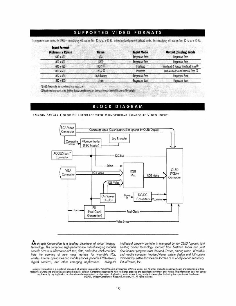
OLEDs will be compatible with night vision goggles, perhaps with assistance of a color filter to block emission in the red. Very importantly, OLEDs should work over the UI temperature range. Qualification of OLED technology for military specification is in progress. To evaluate this technology, we purchased a developer kit for an SVGA (800 × 600) OLED display. SVGA is overkill for UI: we purchased the unit because it is one of the few available at this time with a user interface. We operated the devices in the temperature chamber at –25 °F, room temperature, and at 140 °F (figure 3). For this simple experiment, we placed a charge-coupled device (CCD) camera in the temperature chamber along with the OLED. The OLED output was controlled by a computer. The display operated acceptably at all temperatures. Figure 4 shows the CCD camera output for three operating temperatures. This experiment was intended simply to verify operation of this new class of devices over temperature, and not to characterize the display temperature performance. The CCD camera has not been characterized over temperature, so we cannot separate the temperature effects of the camera from those of the display. However, we think the contrast of the OLED deteriorates as the temperature is decreased, but is acceptable. Documentation for the developer kit is attached in appendix B.

5
Interface
electronics
Computer,
framegrabber
Temperature Chamber
OLED
Display
CCD Camera
Figure 3. Setup for observing the OLED SVGA display at different temperatures.
Figure 4. Images of the SVGA OLED display output at temperatures of (a) –25 °F, (b) room temperature, and (c) 140 °F. A CCD camera was placed in the temperature chamber with the display. A framegrabber was used to record the CCD output. The CCD camera was not calibrated or compensated for temperature changes. We did not attempt to quantify the CCD temperature dependence from that of the OLED. The experiment simply verifies that the OLED functions satisfactorily over the range –25–140 °F. The waviness in the horizontal and vertical lines is software-induced after image acquisition.
a) b)
c)

6
Recently an OLED display (64 × 256 pixels, passive matrix, 1.5 in diagonal) has been incorporated into a commercial product, a cellular phone manufactured by Motorola. The display is made by Tohoku Pioneer Corporation of Japan and is used in the Motorola P8767 phone. We have procured a P8767 for observation of the display. The display is reported to consume significantly less than 5 mW. Currently, this is the only OLED display in a consumer electronics application. Pioneer developed their own driver chip for the OLED. Another driver chip, the SSD1301, has been developed through a Solomon Systech/RiTdisplay Corp. collaboration for 64 × 132 passive matrix OLEDs. We have requested the chip specifications from Solomon.
Mobile Display Systems, an annual publication of Stanford Resources, Inc., gives market research, technology assessment, strategic analysis, and market forecasts for mobile display technologies. The charts and data of figures 5–7 are taken from their 2001 annual report. Figure 5 shows the market forecast for displays with diagonal between 1 and 2 in. For reference, the UI LCD format has ~1 in diagonal dimension, and the SYDET LCD ~1.85 in diagonal. The 1- to 2-in size will be popular for the cell phone market, and we expect there will be a number of different size displays available within this range. The information density will be much greater than that of the UI or SYDET LCDs due to the increased resolution and programmability. Figure 6 breaks out the OLED market for the same size display by application. Cellular phones, particularly those with monochrome displays, are expected to drive OLED production. This chart, and the chart shown in figure 7, show the predicted OLED market for 1- to 2-in diagonal displays. The point is that OLEDs are predicted to command a significant market share and should be a reliable source of display technology through 2007. Specific forecasts beyond 2007 have not been found. The cost of a mass-produced COTS display should be comparable to the SYDET segmented LCD.
2.3 Graphic LCD Displays
As seen in figure 5, the mobile display market will be dominated by super twisted nematic (STN) LCD technologies. These voltage-controlled devices will be available in many formats such as the 64 × 256 OLED discussed. It appears that most of the LCD displays will be emissive, achieved through backlighting; however, reflective graphic LCD display will also be available. To date, no graphic LCDs have been found that will operate at UI cold temperature limit of –25 °F.

7
Figure 5. Total forecast market value for OLED and LCD mobile displays with 1 in ≤ diagonal dimension ≥ 2 in. Market will be dominated by LCD displays, which are not expected to operate satisfactorily at low temperatures. Data from Stanford Resources.
Figure 6. Forecast of market value of OLED displays with 1 in ≤ diagonal dimension ≥ 2 in, active and passive matrix devices. Forecast shows, for example, a $220 million market for monochrome OLEDs of this size in 2004. Data from Stanford Resources.

8
Figure 7. Forecast of market value of OLED displays of all formats. Forecast component values in $ millions. Data from Stanford Resources.
2.4 Display Summary
We see OLED and TN LCD as the candidate technologies for UI. We do not emphasize STN LCD devices because none are known to function at low temperature, but the technology should be monitored until system design begins. The commercial viabilities of other mobile display technologies are not clear (or promising).
We see two critical trades or issues: the information density vs. size and power dissipation trade and the emissive vs. reflective trade.
Both display types, LCD and OLED, will be night vision compatible in that they can be operated at short visible wavelengths not detectable by night vision goggles. The UI could be programmed so that a simple input sequence would shut off an emissive display in an emergency. We are not aware of any real disadvantages of an emissive display, and think that visibility of emissive displays may be better than reflective displays in many environments.
Feedback from use of the emulation program for the UI TN LCD and experience with SYDET as development and use progress should provide input as to whether a “reasonably sized” TN LCD provides sufficient data and cues for UI user programming. We would define a reasonably sized device as one no larger than the SYDET LCD (~1.9 in diagonal). In general, if the SYDET or UI LCD display format are deemed adequate, a TN LCD should be first choice for UI because of low power dissipation, simplicity of the electronic interface, and history of TN LCDs in other military applications. If future changes in the UI ORD call for more functionality, or
9
simultaneous functions, etc., this will exacerbate the information density problem with TN LCD. If information density of TN LCD is not adequate, OLED devices may be used, assuming that devices of appropriate format will be available. We think a 64 × 132 dot matrix format would be adequate for UI. However, we have not developed coding techniques for implementing SYDET functionality with a dot matrix display. We suspect that, for the user, information density for SYDET marginally acceptable at best, that the proposed UI display format is not adequate, and that future additional requirements for UI may complicate the programming, pushing the display choice to OLED technology.
Finally, we comment that an external setting device would eliminate the UI display altogether, saving power and volume, and would result in a more user-friendly user interface.
3. RF Receiver Size Reduction Background
The remotely activated munitions system (RAMS) B RF functionality is shown in figure 8a. In the CY2000 report, we identified a number of large passive components for possible replacement with smaller parts, among them a large inductor in the quadrature detector of the demodulator. This discriminator coil, along with a parallel chip capacitor, presents a 90 phase shift at the final IF frequency (100 kHz for RAMS B) for the quadrature detector. Because the RAMS B Motorola MC3372 FM receiver chip was designed for use in cordless phones, there are off-the-shelf ceramic resonators available for use with the chip. The Murata D455C16 is one such resonator. The Murata resonator is significantly smaller then the coil (~1/4th the volume), but it operates at 455 kHz rather than 100 kHz. The change in the final IF frequency required that we replace the 10.6-MHz crystal for the second local oscillator (LO) with one designed to operate at 10.245 MHz, as well as a few other minor circuit changes. One additional problem with using the Murata resonator is the fact that it is not rated for the full temperature range required for RAMS B. With this in mind, we set up an experiment to compare the sensitivity of three different modifications of the RAMS RF board. Each of the boards uses a different quadrature device. The boards used an air coil, a coil with a ferrite slug core (for tuning, RAMS B), and a ceramic resonator (board #’s 1, 2, and 3 respectively). Thus, boards 1 and 2 implement the schematic of figure 8a, while board 3 implements that of figure 8b.

10
F1BP
Mix1
RF_In
25.5 MHz
LO_1
14.8 MHz
F2BP
10.7 MHzMix2
LO_2
10.6 MHz
Demod
Quad Detector with Inductor: 100 kHz
To MC
a)
F1BP
Mix1
RF_In
25.5 MHz
LO_1
14.8 MHz
F2BP
10.7 MHzMix2
LO_2
10.6 MHz
Demod
Quad Detector with Inductor: 100 kHz
To MCF1BP
Mix1
RF_In
25.5 MHz
LO_1
14.8 MHz
LO_1
14.8 MHz
F2BP
10.7 MHzMix2
LO_2
10.6 MHz
LO_2
10.6 MHz
Demod
Quad Detector with Inductor: 100 kHz
To MC
a)
F1BP
Mix1
RF_In
25.5 MHz
LO_1
14.8 MHz
F2BP
10.7 MHzMix2
LO_2
10.25 MHz
Demod
Quad Detector with ceramic resonator: 455 kHz
To MC
b)
F1BP
Mix1
RF_In
25.5 MHz
LO_1
14.8 MHz
F2BP
10.7 MHzMix2
LO_2
10.25 MHz
Demod
Quad Detector with ceramic resonator: 455 kHz
To MCF1BP
Mix1
RF_In
25.5 MHz
LO_1
14.8 MHz
LO_1
14.8 MHz
F2BP
10.7 MHzMix2
LO_2
10.25 MHz
LO_2
10.25 MHz
Demod
Quad Detector with ceramic resonator: 455 kHz
To MC
b)
Figure 8. RF Block Diagram for (a) RAMS B and (b) experimental configuration using ceramic resonator at 455 kHz.
3.1 Experiment
The experiment is designed to compare the sensitivity of the three different boards vs. temperature. Figure 9 shows a block diagram of the experimental setup. The RF boards are placed in an environmental chamber so the temperature can be controlled. A signal generator (Marconi Model 2022) provides the FM-modulated signal at 25.5 MHz. The Marconi signal generator is externally modulated by a 220-Hz clock (220 Hz is the RAMS B data rate). The spectrum analyzer monitors the RF power input to the board under test, and the counter gives the mean recovered clock rate. The counter can average the clock frequency over 100 or 1000 acquisitions. The 1000-count average is used at the low input power levels where the recovered clock frequencies vary more. This set of measurements gives a relative measure of the sensitivity of the boards.
3.2 Results
Figures 10–12 show the results of the measurements of boards 1, 2, and 3 at various temperatures. The x-axis shows the input power as indicated on the signal generator, and the y-axis shows the mean frequency of the recovered clock signal as measured by the counter. The various curves show the measurements at different temperatures (e.g., red is 80 °C and black is –40 °C).

11
MarconniSignal Generator
Model 2022
RAMSRF board
RFIN
CODEOUT
Wavetek FunctionGenerator
Model KJ-99
Spectrum AnalyzerAdvantest R3271
Universal Counter
HP5335A
IN
RFOUT
OUT
External FM MODULATION
220HzSquare Wave
25.5MHz
Environmental Chamber
Figure 9. Block diagram of the experimental setup.
110 105 100 95 90 85 80 75 70200
250
300
350
400
450
500
806040200-20-40
Board #1
Signal Power (dBm)
Mea
n F
req. (H
z)
Figure 10. Plot of mean frequency vs. input signal power for different
temperatures, board 1 (air coil).

12
110 105 100 95 90 85 80 75 70200
250
300
350
400
450
500
806040200-20-40
Board #2
Signal Power (dBm)
Mea
n F
req
. (H
z)
Figure 11. Plot of mean output frequency vs. input signal power for different temperatures, board 2 (iron powder core).
Because input clock frequency is 220 Hz, deviation of the curves from 220 is a good indication that the receiver sensitivity is not sufficient and data recovery errors are occurring. The breakpoint sensitivity (sensitivity value where the waveforms begin to deviate from 220 Hz) is ~ –100, –97, and –82 dBm for boards 1, 2, and 3, respectively. In addition, the amount of spread of the data curves in the breakpoint area of each plot is a good indication of the temperature sensitivity. The temperature sensitivity of the boards is 3, 5, and 7 dB for boards 1 (air core), 2 (ferrite core), and 3 (ceramic resonator), respectively.

13
110 105 100 95 90 85 80 75 70200
250
300
350
400
450
500
6040200-20-40
Signal Power (dBm)
Mea
n F
req. (H
z)
Board 3
Figure 12. Plot of mean output frequency vs. input signal power for different temperatures, board 3 (ceramic resonator).
3.3 RF Experiment Conclusions
As expected, the sensitivity is best with the air core coil (board 1), followed by the ferrite core coil (board 2), and the ceramic resonator (board 3). To give an idea of the effect of the reduced sensitivity on range, we can use the formula for the free space loss ratio (SLR).
SLR λ
..4 π R
2, (1)
which is the power lost over the distance R for wavelength λ. Taking the ratio of sensitivities (P1 and P2) gives
P1P2
R2R1
2
. (2)
We can then use the sensitivities quoted in the previous paragraph to calculate the theoretical relative ranges of the receiver boards (relative to board 1). The ranges are 1, 0.708, and 0.126 for boards 1, 2, and 3, respectively. Similarly, the air core coil is the least temperature sensitive, and the ceramic resonator shows the most variation with temperature. For practical reasons, the configuration of board 2 is used in RAMS B field hardware. Comparing theoretical ranges of

14
boards 2 and 3, we see that the resonator configuration will have ~18% of the range of the current RAMS B field hardware. In addition to the problems of less sensitivity and more temperature dependence, the ceramic resonator was off-frequency slightly. When we initially tested the ceramic resonator with the fixed 10.245-MHz crystal, the sensitivity was even lower than that depicted in figure 12 (–74 dB as opposed to –84 dB). For this reason, we decided to use an external oscillator so we could tune the circuit for optimum sensitivity. For reference, RAMS B hardware is also hand-tweaked for maximum sensitivity. The measurements shown in figure 12 were made at optimum local oscillator tuning (fLO = 10.2362 MHz). This would necessitate hand picking the correct resonator out of a large sample of resonators to get reasonable performance. For this reason and the reduced range, as previously mentioned, we would not recommend using the ceramic resonator.
4. CY2001 Research Summary
We have conducted market research in the area of display devices and have made a qualitative comparison of the leading candidate technologies and discussed general trades. We obtained a sample display made with an emerging technology (OLED) and verified performance over temperature, and provided a market forecast for this technology. We developed a straw-man design for a miniature segmented TN LCD display and wrote a graphical emulation program of a programming sequence.
For miniaturization of the current RAMS B RF receiver section, we conducted research, a market survey, and laboratory tests related to replacement of a large inductor with a much smaller ceramic resonator. We redesigned a section of the RF circuit to accommodate the resonator according to manufacturer’s specifications, and conducted sensitivity measurements over temperature for three different designs. Results for the three designs were compared for range sensitivity, and a recommendation was made to retain the RAMS B inductor design, mainly because of greater sensitivity.
In a related task that will be delivered separately, we have designed and constructed a working functional prototype of a unit that contains RAMS and SYDET capability.

15
Appendix A. UI TN LCD Flow Chart
Select the TIME DELAY (T) or SYDET (S)
options in the Operations Mode (OP) using the
SELECT key.
[SYDET option must be selected]
SET CURRENT TIME
(CT)
(Goto Time Entry
Subroutine)
Select the RELATIVE (R) or ABSOLUTE (A)
options in the Time Reference Mode (TR)
using the SELECT key.
[ABSOLUTE option must be selected]
SET ACTIVATION
TIME
(AT)
(Goto Time Entry
Subroutine)
SET FUNCTION TIME
(FT)
(Goto Time Entry
Subroutine)
Select the AIR (A), SURF (S), and WATER
(H2) options in the SET ENVIRONMENT
Mode (E) using the SELECT key.
[AIR option must be selected]
Select the FIELD (F), SNOW (S), JUNGLE (J),
and URBAN (U) options in the SET LOCALE
Mode (LO) using the SELECT key.
•Turn ON
SELECT
NEXT
SELECT
NEXT
VERIFY
SELECT
NEXT
A
Set YEAR (Y)
5 Min Safe Separation
A
VERIFY
VERIFY
Set Month (MO)
Set Day (D)
Set Hour (H)
Set Minute (MI)
<Time Entry Subroutine>
VERIFY
VERIFY
VERIFY
VERIFY
VERIFY
SELECT
NEXT
Select the TIME DELAY (T) or SYDET (S)
options in the Operations Mode (OP) using the
SELECT key.
[SYDET option must be selected]
SET CURRENT TIME
(CT)
(Goto Time Entry
Subroutine)
Select the RELATIVE (R) or ABSOLUTE (A)
options in the Time Reference Mode (TR)
using the SELECT key.
[ABSOLUTE option must be selected]
SET ACTIVATION
TIME
(AT)
(Goto Time Entry
Subroutine)
SET FUNCTION TIME
(FT)
(Goto Time Entry
Subroutine)
Select the AIR (A), SURF (S), and WATER
(H2) options in the SET ENVIRONMENT
Mode (E) using the SELECT key.
[AIR option must be selected]
Select the FIELD (F), SNOW (S), JUNGLE (J),
and URBAN (U) options in the SET LOCALE
Mode (LO) using the SELECT key.
•Turn ON
SELECT
NEXT
SELECT
NEXT
VERIFY
SELECT
NEXT
A
Set YEAR (Y)
5 Min Safe Separation
A
VERIFY
VERIFY
Set Month (MO)
Set Day (D)
Set Hour (H)
Set Minute (MI)
<Time Entry Subroutine>
VERIFY
VERIFY
VERIFY
VERIFY
Set Month (MO)
Set Day (D)
Set Hour (H)
Set Minute (MI)
<Time Entry Subroutine>
VERIFY
VERIFY
VERIFY
VERIFY
VERIFY
SELECT
NEXT

16
INTENTIONALLY LEFT BLANK.

17
Appendix B. Organic Light Emitting Diode (OLED)

18
19

20
INTENTIONALLY LEFT BLANK.

21
Distribution
Admnstr Defns Techl Info Ctr ATTN DTIC-OCP (Electronic copy) 8725 John J Kingman Rd Ste 0944 FT Belvoir VA 22060-6218 US Army Rsrch Lab ATTN AMSRD-ARL-CI-IS Mail & Records Mgmt ATTN AMSRD-ARL-CI-OK-T Techl Pub (2 copies) ATTN AMSRD-ARL-CI-OK-TL Techl Lib (2 copies) ATTN AMSRD-ARL-D J M Miller ATTN AMSRD-ARL-SE-EE B Lawler (10 copies) ATTN AMSRD-ARL-SE-RE D Judy Adelphi MD 20783-1197