size reduction and performance improvement of a microstrip
TRANSCRIPT
1
Vol.:(0123456789)
Scientific Reports | (2021) 11:7773 | https://doi.org/10.1038/s41598-021-87477-4
www.nature.com/scientificreports
Size reduction and performance improvement of a microstrip Wilkinson power divider using a hybrid design techniqueMohammad Behdad Jamshidi1,2, Saeed Roshani3, Jakub Talla1,2, Sobhan Roshani3* & Zdenek Peroutka1,2
In the design of a microstrip power divider, there are some important factors, including harmonic suppression, insertion loss, and size reduction, which affect the quality of the final product. Thus improving each of these factors contributes to a more efficient design. In this respect, a hybrid technique to reduce the size and improve the performance of a Wilkinson power divider (WPD) is introduced in this paper. The proposed method includes a typical series LC circuit, a miniaturizing inductor, and two transmission lines, which make an LC branch. Accordingly, two quarter-wavelength branches of the conventional WPD are replaced by two proposed LC branches. Not only does this modification lead to a 100% size reduction, an infinite number of harmonics suppression, and high-frequency selectivity theoretically, but it also results in a noticeable performance improvement practically compared to using quarter-wavelength branches in the conventional microstrip power dividers. The main important contributions of this technique are extreme size reduction and harmonic suppression for the implementation of a filtering power divider (FPD). Furthermore, by tuning the LC circuit, the arbitrary numbers of unwanted harmonics are blocked while the operating frequency, the stopband bandwidth, and the operating bandwidth are chosen optionally. The experimental result verifies the theoretical and simulated results of the proposed technique and demonstrates its potential for improving the performance and reducing the size of other similar microstrip components.
As modern communication systems have grown rapidly, the demands for microwave components with low energy loss, compact size, and filtering response have increased significantly. In this regard, wireless components should be integrated for the multiple function ability in embedded systems. For example, integrating a filter with a power divider will result in a compact size and low energy loss in the microwave components. Power dividers and couplers are two important microstrip passive components that can benefit from such modifications. Accord-ingly, they can have more appropriate harmonic suppression and higher performance than the conventional ones, leading to higher efficiency in aspects of the performance and energy1,2.
Power dividers play an important role in modern wireless communication systems3. Wilkinson power divider (WPD) is one of the most popular types of dividers. In fact, the WPD was first proposed by Ernest J. Wilkinson in 19604. Since then it has widely used in modern communication systems, such as Doherty power amplifiers5, balanced power amplifiers6,7, push–pull power amplifiers8, antenna feed networks9, phase shifters10, and RF/microwave frontend systems11.
One of the disadvantages of the typical WPD is that the spurious harmonics can easily pass through the power divider paths and decrease its performance. Another disadvantage of the WPD is its large size, which is about approximately 0.0156 λ2. Recently, several approaches have been proposed and performed to solve these problems. For example, coupled lines12, open-ended stubs13, T-shaped and Π-shaped resonators14, and embed-ded filters15.
Open-ended stubs are usually used in the main quarter wavelength branches of the divider as studied in13,16 to reduce the size and suppress a few harmonics. Open-ended stubs can also be used at the input port to improve the
OPEN
1Research and Innovation Centre for Electrical Engineering (RICE), University of West Bohemia, Pilsen, Czech Republic. 2Department of Power Electronics and Machines (KEV), University of West Bohemia, Pilsen, Czech Republic. 3Department of Electrical Engineering, Kermanshah Branch, Islamic Azad University, Kermanshah, Iran. *email: [email protected]

2
Vol:.(1234567890)
Scientific Reports | (2021) 11:7773 | https://doi.org/10.1038/s41598-021-87477-4
www.nature.com/scientificreports/
input return loss parameter17–19. Applying open-ended stubs technique causes to provide desirable transmission zeros at the frequency response, which can suppress the desired harmonics and reduce the size20. However, the drawback of this method is to provide a single transmission zero. Hence, for obtaining a wide stopband several open-ended stubs should be applied13. Nevertheless, increasing the numbers of such stubs may contribute to the overall size and make the design more complicated.
Another technique, which has been used in several pieces of research, is the use of coupled lines21,22. Applying coupled lines in the divider structure can produce several transmission zeros and increase the operating band-width of the divider. Wang et al. utilized coupled lines in a WPD to obtain wideband and harmonic suppression21. However, the WPD designed in21 had a rather large size compared to the conventional divider. Furthermore, parallel-coupled lines to present a filtering power divider (FPD) with a filtering response were used in22. The frequency response of this divider was wideband with a filtering shape, but the size reduction was not achieved. Moreover, stepped impedance resonators to improve the performances of the dividers were applied23,24 and a dual-band filtering divider was introduced in23. In the presented divider in21, the stepped impedance resonators were applied to provide filtering response in operating frequencies, but the overall size of the divider was qui-etly large. In addition, the stepped impedance resonators for harmonic suppression in WPD were utilized in24. However, the obtained suppressing bandwidth was narrow and the designed WPD had a large size.
In fact, microstrip filters can suppress the desired frequency band; therefore, they can be embedded in the divider to make a filtering divider25. In this respect, substrate integrated waveguide (SIW) with embedded filters to design a filtering power divider were used in15, and multiple isolation resistors technique was also presented in15 in order to improve the divider isolation. Nonetheless, the overall size of the divider was very larger than the conventional divider.
Moreover, Chao and Li introduced a new technique to design an FPD, in which a resistor-inductor-capacitor isolation network was employed 26. While using lumped elements to design the suggested network in 26 was con-sidered analytically, no lumped elements, such as inductors or capacitors were applied practically. Indeed, only microstrip lines were utilized in the fabrication stage. Disregarding the implementation of the introduced FDP in 26, the parallel inductor and capacitor were placed between output ports to achieve filtering response, but the suppression bandwidth was not wide enough and only the second harmonic was suppressed. Due to inserting the parallel inductor and capacitor between output ports, the high suppression band was not achieved in 26. In other words, this mechanism could only improve the isolation between the output ports (S32) and was not able to amend the filtering response (S21) effectively. Although it was claimed that “a miniaturized divider is obtained” in 26, the divider size is even larger than the first WPD made by E.J Wilkinson in 1960.
In another work27, A. Chen et al. added two capacitors in parallel with the transmission lines in a WPD to provide a new zero-reflection frequency, which resulted in a wider bandwidth compared to the conventional WPD. Although they designed a tunable WPD with a broad operating band, neither remarkable size reduction nor noteworthy harmonics suppression was achieved using the capacitors, which were added to the proposed WPD in27. According to the results of27, only the second harmonic was suppressed, which is not a desirable performance compared to some pieces of research13,14,16,19,21–23, and more importantly, size reduction was only around 23% that is not impressive for a WPD. Besides, the length of the long quarter wavelength branches, in the designed divider in27, was not reduced, but these branches were bent to achieve a limited size reduction.
On the other hand, combinations of different structures have been used in order to improve the characteristics of WPDs in some methods23,28,29. For instance, in28 the stepped impedance and open-ended stubs were combined, whereas stepped impedance, open-ended stubs, and coupled lines were employed to design a filtering divider in29. In addition, lumped elements, coupled lines, and open-ended stubs techniques were gathered to design a harmonic suppressed divider with a wide operating band in29.
As reviewed above, limited improvement in harmonic suppression and some restrictions in reducing the size should be taken into account as two important issues in the design of WPDs in all of the aforementioned methods. In the present paper, a novel hybrid method is proposed using LC branches in both paths of the divider to improve the performance of the WPD. In this regard, an infinite number of harmonics suppression and 100% size reduction can be achieved theoretically. Although, in practice, it is impossible to reach 100% size reduction and the infinite number of harmonics suppression, the extreme size reduction and large numbers of harmonic suppression are obtained, which has not been achieved in any divider so far. Most importantly, an analytical and flexible design method is offered, in which all of the key specifications of the WPDs can be chosen arbitrarily by the designers or manufacturers based on consumer tastes. These specifications include size reduction percentage, the number of harmonics suppression, operating frequency, and operating bandwidth.
The paper organization is demonstrated as follows. In “Typical structure of a microstrip Wilkinson power divider”, the conventional WPD and its fundamentals are described. In “Proposed WPD structure”, it is explained that how the proposed LC branches structure is applied in a typical WPD. The analytical equations of the introduced divider are then illustrated in “Analyses of the proposed WPD”. In “Design Examples at 2.4 GHz” and “Design examples at 0.8 GHz”, two design examples at 2.4 GHz and two design examples at 0.8 GHz are presented to verify the performance of the proposed structure in different frequencies and different dimensions. In “Measurement results”, the analytical and simulation results of the proposed structure are verified using experimental results. Finally, in the last “Conclusions”, the summary of the proposed method, its potentials, and conclusions are described.
Typical structure of a microstrip Wilkinson power dividerIn this section, the fundamentals and basics of a typical WPD are described. In such components, quarter-wave-length branches are responsible to suppress the unwanted harmonics and passing the main frequency. Figure 1 illustrates a classic WPD with two quarter-wavelength branches and a resistor between output ports. One of

3
Vol.:(0123456789)
Scientific Reports | (2021) 11:7773 | https://doi.org/10.1038/s41598-021-87477-4
www.nature.com/scientificreports/
the most challenging drawbacks with such structures is to have a large size due to utilizing the large quarter-wavelength branches, which are not favorable in modern wireless systems. Another important disadvantage, which can be mentioned for this type of design, is to suffer from the existence of spurious harmonics because the typical quarter-wavelength branches cannot provide a suppression band for the divider. Nevertheless, the WPD layout structure plays an important role in determining the overall size of WPDs. Generally, two common forms of the WPD have been utilized in the design of WPDs, namely squared-shape and circular-shaped, which are depicted in Fig. 2a and b, respectively. As you can see in Fig. 2a, the overall size of the square-shaped WPD, is 0.125 λ × 0.125 λ, which is equal to 0.0156 λ2 while the overall size for circular one is 0.0198 λ2, indicating this point that the circular type of the WPD is typically larger than the square-shaped one. It should be noted that in both square-shaped and circular-shaped WPDs, the size of the resistor is neglected in calculation of the total size theoretically. Regardless of this difference, the size of WPD and many other microstrip components significantly depend on their quarter-wavelength branches, such as branch-line couplers, rat-race couplers, and several types of discrete power amplifiers. The proposed structure will be discussed in the next section.
Proposed WPD structureAs is mentioned, the typical WPD suffers from large size and spurious harmonics existence. Therefore, by modi-fying the transmission lines used in the WPD that are more responsible in increasing the size, not only will the size of components made by this technology be far more compact, but it can also lead to increasing the efficiency. Overall, to reach these objectives, some important parameters like selectivity and suppressing the unwanted harmonics should be considered. In this regard, a novel hybrid solution to improve the size and performance of a WPD has been presented here. In addition, the proposed method can be used in a wide range of microstrip components using transmission lines.
Proposed LC branch lines. The proposed method includes replacing long quarter wave length transmis-sion lines, which are used in WPDs or any other microwave components, such as filters, diplexers, matching networks, couplers, and power amplifiers, with the proposed compact LC branches. Figure 3 demonstrates the proposed hybrid approach using microstrip lines and LC branches in a microwave component. As is observed in Fig. 3, microstrip branch lines of the conventional WPD are replaced by the proposed LC branch lines. The LC branch lines include a resonance capacitor (C0), a resonance inductor (L0), a miniaturizing inductor (Lm), and two transmission lines (Z1, θ1). The resonance capacitor and inductor, which form a series LC circuit, should be tuned at the desired operating frequency (f0). The series LC circuit is shorted at f0 while it is opened at other frequencies, resulting in the bandpass response of the divider. Therefore, the LC branch structure can be used to reduce the desired harmonics.
Figure 1. The arrangement of microstrip transmission lines to design a typical WPD.
Figure 2. The arrangements of microstrip transmission lines in classic WPD layout; (a) square-shaped WPD layout; (b) circular-shaped WPD layout.

4
Vol:.(1234567890)
Scientific Reports | (2021) 11:7773 | https://doi.org/10.1038/s41598-021-87477-4
www.nature.com/scientificreports/
Furthermore, the size of each microstrip branch line significantly decreases from a large size to a very small size that will be discussed in the next sections. In fact, the miniaturizing inductor results in reducing the LC branch length. The inductances of L0 and Lm are in series and can be considered as the inductance of L in practice. After applying the proposed LC branches, a new structure will be obtained for the WPD. The proposed structure of the WPD with the presented LC branches is shown in Fig. 4.
Analyses of the proposed WPDThe structure of the proposed WPD is analyzed using the ABCD matrix. The ABCD matrix of the proposed LC branch has to be equaled to the ABCD matrix of a conventional quarter wavelength (QWL) branch. Therefore, the obtained equation is written in Eq. (1)
where, in M1, MLCB, and MQWL are ABCD matrices of the transmission line (Z1, θ1), LC branch (LCB), and quarter wavelength line (
√2 Z0, λ/4), respectively. In addition, the values of M1, MLCB, and MQWL matrices are
defined in Eq. (2).
As mentioned before, the series L0C0 is tuned at the main frequency (f0), which is shorted at the main fre-quency. Hence, if it is assumed to perform the analyses in the main frequency, the LC branch matrix can be simplified as written in Eq. (3).
(1)M1× MLCB× M1= MQWL
(2)
M1 =[
cos (θ1) jZ1 sin (θ1)jY1 sin (θ1) cos (θ1)
]
,
MLCB =[
1 jLmω + jL0ω − j/(C0ω)0 1
]
,
MQWL =[
0 j√2Z0
j/√2Z0 0
]
Figure 3. The main idea of replacing the microstrip lines with the proposed LC branches.
Figure 4. The proposed structure of the WPD with the presented LC branches.

5
Vol.:(0123456789)
Scientific Reports | (2021) 11:7773 | https://doi.org/10.1038/s41598-021-87477-4
www.nature.com/scientificreports/
By solving Eq. (1), three independent equations are obtained as follows
By comparing Eqs. (5) and (6), the following equation is achieved.
By solving Eq. (7), which is a second-order equation, the normalized value of Z1 can be calculated as written in Eq. (8).
Figure 5 demonstrates the proposed approach, including the prototype of a microstrip WPD and the sug-gested method to solve the equations in order to obtain circuit parameters. As it can be seen in this figure, in the first stage, the prototype of the understudied component is indicated. In the second stage, the values of the key parameters for the component, such as the amount of size reduction (SR%), operating frequency (f), and operating bandwidth are arbitrarily determined. Next, θ1 is computed based on the selected SR% in the previous stage. In the third stage, Z1 is calculated using Eq. (8). The calculated circuit values in the third stage are listed in Table 1 at the operating frequency of 2.4 GHz and 0.8 GHz. In the fourth stage, the value of Lm is obtained by using Eq. (4). As is observed, the value of Z1 is independent of the operating frequency, while the value of Lm depends on the operating frequency. By adding L0 and Lm, the total value of L is achievable in the fifth stage. The values of L0 and C0 are achieved based on values of Q (quality factor) being available in Tables 2 and 3 at the operating frequency of 2.4 GHz and 0.8 GHz. Besides, the value of Q is obtained through bandwidth, which will be more discussed at the next Sections. Finally, the new proposed divider with desirable parameters based on (θ1, Z1, C0, and L) can be achieved.
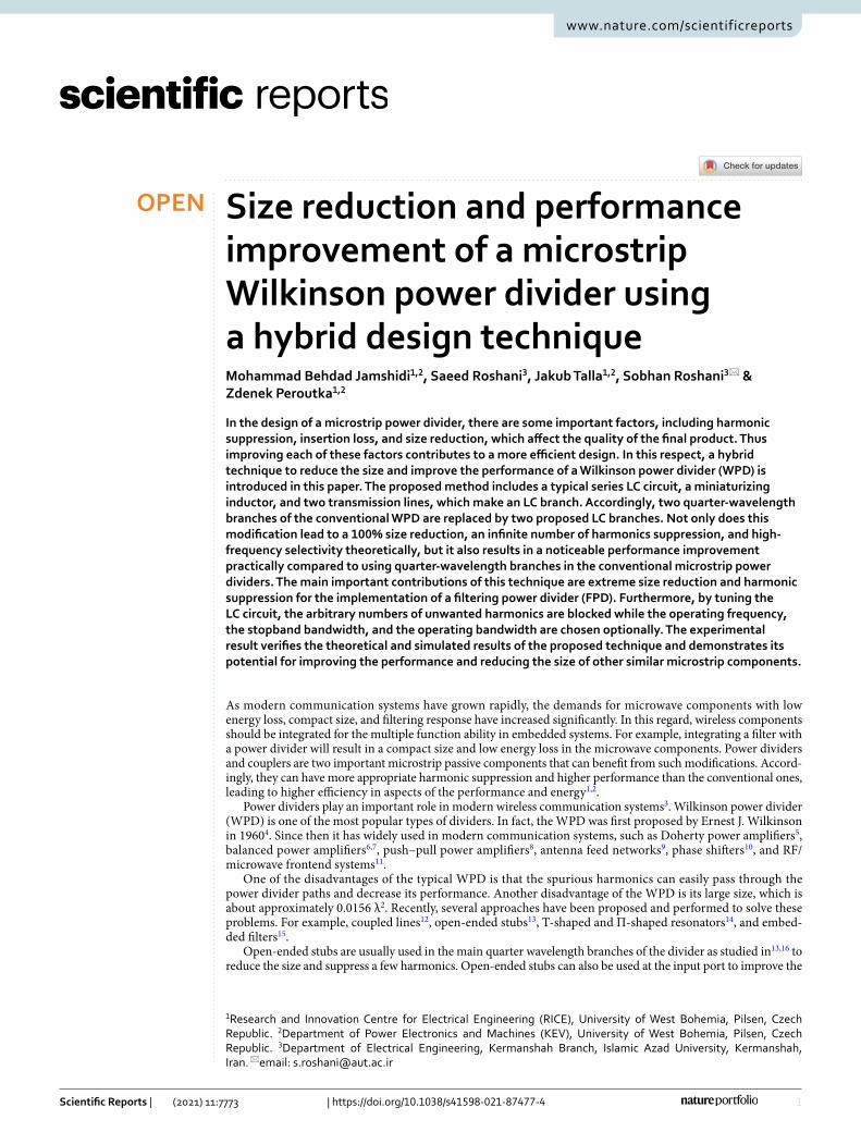
The design process of the proposed technique is described in Fig. 5. In addition, some design examples for circuit parameters values are calculated and shown in Table. 1. Moreover, the relation between calculated circuit parameters from the analysis is shown in Fig. 6 for more clarification. The calculated values of divider maximum size reduction versus total electrical length of the branch and versus the value of Z1 (Ω) are demonstrated in Fig. 6a and b. The word "maximum" is used for maximum size reduction because the L and C component ele-ments occupy a small size practically, which is not considered in the theory design. As mentioned above, the main branch line length of the conventional WPD is λ/4, while the proposed LC branch length is considered 2θ1. Therefore, the maximum size reduction is calculated according to the ratio of the size of the square shape WPD with the proposed LC branches to the size of the conventional square shape WPD with typical λ/4 branches. Figure 6b illustrates the lower size of the divider which is corresponding with the lower value of Z1, leading to a wider transmission line. Moreover, the calculated values of Z1 (Ω) versus the total electrical length of the branch are depicted in Fig. 6c. As can be seen in Fig. 6c, the lower size of the divider is corresponding with the wider transmission line. Besides that, Fig. 6d shows the calculated inductance Lm values versus maximum size reduction at different frequencies. According to this figure, the higher values of Lm are needed for higher size reduction and lower operating frequencies. Therefore, the values of Z1 are independent of the operating frequency, while the value of Lm depends the on operating frequency. Additionally, from both analyses and Fig. 6, it can be con-cluded that any value of maximum size reduction can be theoretically achieved using the proposed LC branches.
In the final design, in addition to Lm, resonant inductor (L0) and capacitor (C0) will be applied to form the LC branch. The series LC circuit should be tuned at the desired operating frequency. For a better explanation of the design procedures, four design examples are introduced, two of them are at 2.4 GHz and two others are at 0.8 GHz. These design examples are comprehensively described in the next section.
Design examples at 2.4 GHzTo verify the analytical results, two design examples at the operating frequency of 2.4 GHz are introduced in this section.
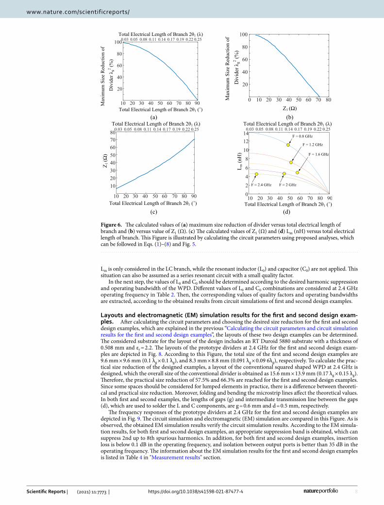
Calculating the circuit parameters and circuit simulation results for the first and second design examples. Some examples for circuit parameter values with different size reductions are calculated and shown in Table. 1. The size reduction values of 55.5% and 69.1% are chosen for the first and second design examples, respectively, both at 2.4 GHz. The circuit parameters for the first and second design examples can be determined according to the assumed values of size reduction and operating frequency. From Table 1, the width
(3)MLCB =[
1 jLmω0 1
]
(4)2Z1 = Lmω0 tan (2θ1)
(5)√2 =
Z1
Z0sin (2θ1)+
Lmω0
2Z0+
Lmω0
2Z0cos (2θ1)
(6)1√2=
Z0
Z1sin (2θ1)−
Z0Lmω0
2Z21
+Z0Lmω0
2Z21
cos (2θ1)
(7)2−Z21
Z20
=
√2Lmω0
Z0
(8)Z1
Z0=
−√2+
√
2+ tan (2θ1)2
tan (2θ)

6
Vol:.(1234567890)
Scientific Reports | (2021) 11:7773 | https://doi.org/10.1038/s41598-021-87477-4
www.nature.com/scientificreports/
Figure 5. The process of design and solving the equations of a WPD based on the proposed technique. First, the conventional WPD with 0% size reduction, no harmonic suppression and no bandwidth tuning ability is considered. The desired values of SR%, operating frequency, and bandwidth are then assumed arbitrarily. Next, with the use of the proposed analyses, the equations are solved and the desired circuit parameters (θ1, Z1, C0, and L) are achieved. By applying these circuit parameters, and the proposed structure to the typical WPD, the new compact divider with desirable SR%, extreme harmonic suppression, and desirable operating bandwidth is obtained.

7
Vol.:(0123456789)
Scientific Reports | (2021) 11:7773 | https://doi.org/10.1038/s41598-021-87477-4
www.nature.com/scientificreports/
(Z1) and length (θ1) dimensions of LC branches transmission lines are 40.8 Ω and 30˚ for 55.5% size reduction, while they are 33 Ω and 25° for 69.1% size reduction, respectively. The values of Lm are calculated equal to 3.1 nH and 3.7 nH for 55.5% and 69.1% size reduction values, respectively. In the next step, the series L0C0 circuit should be tuned at the operating frequency. However, the quality factor (Q) of the series L0C0 circuit can be tuned by changing the L0 and C0 values. The results of the circuit simulations for the first and second design examples at 2.4 GHz are illustrated in Fig. 7. Accordingly, the effects of the series L0C0 circuit with different quality factors on the simulated frequency responses of the presented design examples are shown in this figure. As can be seen in Fig. 7, by increasing the quality factor, the bandwidth decreases, whereas the stopband increases. In other words, by increasing the quality factor more harmonic suppression can be achieved. Therefore, the arbitrary bandwidth can be achieved by tuning the quality factor in LC branches. In the case indicated with “only Lm” in Fig. 7, the
Table 1. The calculated circuit values of the divider for the desired values of the size reduction in two operating frequencies of 2.4 GHz and 0.8 GHz.
Total electrical length of branch 2θ1 (°) θ1 (°) Z1 (Ω)Lm (nH)@2.4 GHz
Lm (nH)@0.8 GHz
Maximum size (λg2) reduction of
divider (%)
90° (0.25 λ) 45° (0.12 λ) 70.7 0 0 0
80° (0.22 λ) 40˚ (0.11 λ) 59.3 1.4 4.2 21
70˚ (0.19 λ 35° (0.10 λ) 49.5 2.4 7.2 39.5
60° (0.17 λ) 30° (0.08 λ) 40.8 3.1 9.4 55.5
50° (0.14 λ) 25° (0.07 λ) 33.0 3.7 11 69.1
40° (0.11 λ) 20˚ (0.05 λ) 25.7 4.0 12.2 80.2
30° (0.08 λ) 15°° (0.04 λ) 18.9 4.3 13 88.9
20° (0.05 λ) 10° (0.03 λ) 12.4 4.5 13.6 95
10° (0.03 λ) 5° (0.01 λ) 6.2 4.6 14 98.7
Table 2. Values of L0, C0, quality factor (Q), and operating bandwidth (BW) at 2.4 GHz operation frequency for the first and second design examples.
C0 (pF)55.5% SR
L0 (nH)55.5% SR
Lm (nH)55.5% SR
L (nH)55.5% SR
BW (MHz)55.5% SR
Q55.5% SR
0.2 22 3.1 25.1 600 4
0.5 8.8 3.1 11.9 1280 1.9
0.8 5.5 3.1 8.6 1830 1.3
1 4.4 3.1 7.5 2130 1.1
C0 (pF)69.1% SR
L0 (nH)69.1% SR
Lm (nH)69.1% SR
L (nH)69.1% SR
BW (MHz)69.1% SR
Q69.1% SR
0.2 22 3.7 25.7 500 4.8
0.5 8.8 3.7 12.5 1200 2
0.8 5.5 3.7 9.2 1650 1.4
1 4.4 3.7 8.1 1950 1.2
Table 3. Values of L0, C0, quality factor (Q) and operating bandwidth (BW) at 0.8 GHz operation frequency for the third and fourth design examples.
C0 (pF)69.1% SR
L0 (nH)69.1% SR
Lm (nH)69.1% SR
L (nH)69.1% SR
BW (MHz)69.1% SR
Q69.1% SR
0.2 198 11 209 75 10.7
0.5 79.2 11 90.2 150 5.3
0.8 49.5 11 60.5 230 3.5
1 39.6 11 50.6 300 2.7
C0 (pF)80.2% SR
L0 (nH)80.2% SR
Lm (nH)80.2% SR
L (nH)80.2% SR
BW (MHz)80.2% SR
Q80.2% SR
0.2 198 12.2 210.2 70 11.4
0.5 79.2 12.2 91.4 140 5.7
0.8 49.5 12.2 61.7 200 4
1 39.6 12.2 51.8 260 3
8
Vol:.(1234567890)
Scientific Reports | (2021) 11:7773 | https://doi.org/10.1038/s41598-021-87477-4
www.nature.com/scientificreports/
Lm is only considered in the LC branch, while the resonant inductor (L0) and capacitor (C0) are not applied. This situation can also be assumed as a series resonant circuit with a small quality factor.
In the next step, the values of L0 and C0 should be determined according to the desired harmonic suppression and operating bandwidth of the WPD. Different values of L0 and C0 combinations are considered at 2.4 GHz operating frequency in Table 2. Then, the corresponding values of quality factors and operating bandwidths are extracted, according to the obtained results from circuit simulations of first and second design examples.
Layouts and electromagnetic (EM) simulation results for the first and second design exam-ples. After calculating the circuit parameters and choosing the desired size reduction for the first and second design examples, which are explained in the previous “Calculating the circuit parameters and circuit simulation results for the first and second design examples”, the layouts of these two design examples can be determined. The considered substrate for the layout of the design includes an RT Duroid 5880 substrate with a thickness of 0.508 mm and εr = 2.2. The layouts of the prototype dividers at 2.4 GHz for the first and second design exam-ples are depicted in Fig. 8. According to this Figure, the total size of the first and second design examples are 9.6 mm × 9.6 mm (0.1 λg × 0.1 λg), and 8.3 mm × 8.8 mm (0.091 λg × 0.09 6λg), respectively. To calculate the prac-tical size reduction of the designed examples, a layout of the conventional squared shaped WPD at 2.4 GHz is designed, which the overall size of the conventional divider is obtained as 15.6 mm × 13.9 mm (0.17 λg × 0.15 λg). Therefore, the practical size reduction of 57.5% and 66.3% are reached for the first and second design examples. Since some spaces should be considered for lumped elements in practice, there is a difference between theoreti-cal and practical size reduction. Moreover, folding and bending the microstrip lines affect the theoretical values. In both first and second examples, the lengths of gaps (g) and intermediate transmission line between the gaps (d), which are used to solder the L and C components, are g = 0.6 mm and d = 0.5 mm, respectively.
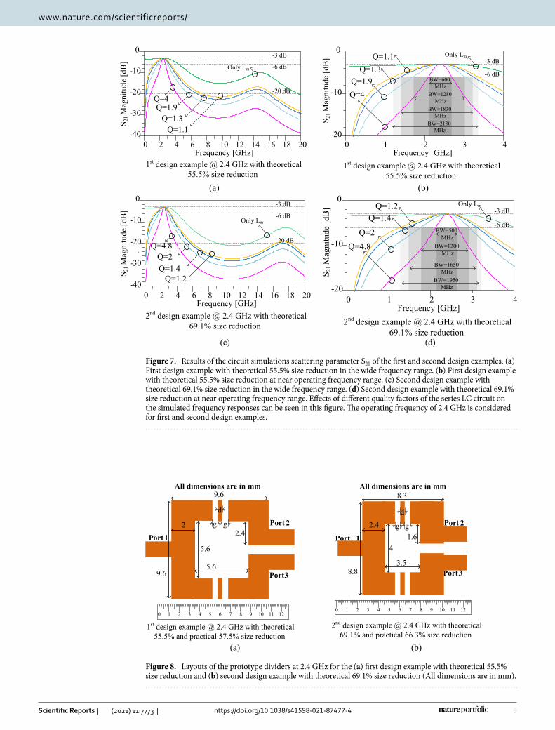
The frequency responses of the prototype dividers at 2.4 GHz for the first and second design examples are depicted in Fig. 9. The circuit simulation and electromagnetic (EM) simulation are compared in this Figure. As is observed, the obtained EM simulation results verify the circuit simulation results. According to the EM simula-tion results, for both first and second design examples, an appropriate suppression band is obtained, which can suppress 2nd up to 8th spurious harmonics. In addition, for both first and second design examples, insertion loss is below 0.1 dB in the operating frequency, and isolation between output ports is better than 35 dB in the operating frequency. The information about the EM simulation results for the first and second design examples is listed in Table 4 in "Measurement results" section.
Figure 6. The calculated values of (a) maximum size reduction of divider versus total electrical length of branch and (b) versus value of Z1 (Ω). (c) The calculated values of Z1 (Ω) and (d) Lm (nH) versus total electrical length of branch. This Figure is illustrated by calculating the circuit parameters using proposed analyses, which can be followed in Eqs. (1)–(8) and Fig. 5.
9
Vol.:(0123456789)
Scientific Reports | (2021) 11:7773 | https://doi.org/10.1038/s41598-021-87477-4
www.nature.com/scientificreports/
Figure 7. Results of the circuit simulations scattering parameter S21 of the first and second design examples. (a) First design example with theoretical 55.5% size reduction in the wide frequency range. (b) First design example with theoretical 55.5% size reduction at near operating frequency range. (c) Second design example with theoretical 69.1% size reduction in the wide frequency range. (d) Second design example with theoretical 69.1% size reduction at near operating frequency range. Effects of different quality factors of the series LC circuit on the simulated frequency responses can be seen in this figure. The operating frequency of 2.4 GHz is considered for first and second design examples.
Figure 8. Layouts of the prototype dividers at 2.4 GHz for the (a) first design example with theoretical 55.5% size reduction and (b) second design example with theoretical 69.1% size reduction (All dimensions are in mm).
10
Vol:.(1234567890)
Scientific Reports | (2021) 11:7773 | https://doi.org/10.1038/s41598-021-87477-4
www.nature.com/scientificreports/
Design examples at 0.8 GHzTwo design examples at the operating frequency of 0.8 GHz (third and fourth design examples) are introduced in this section to verify the analytical results at different frequencies.
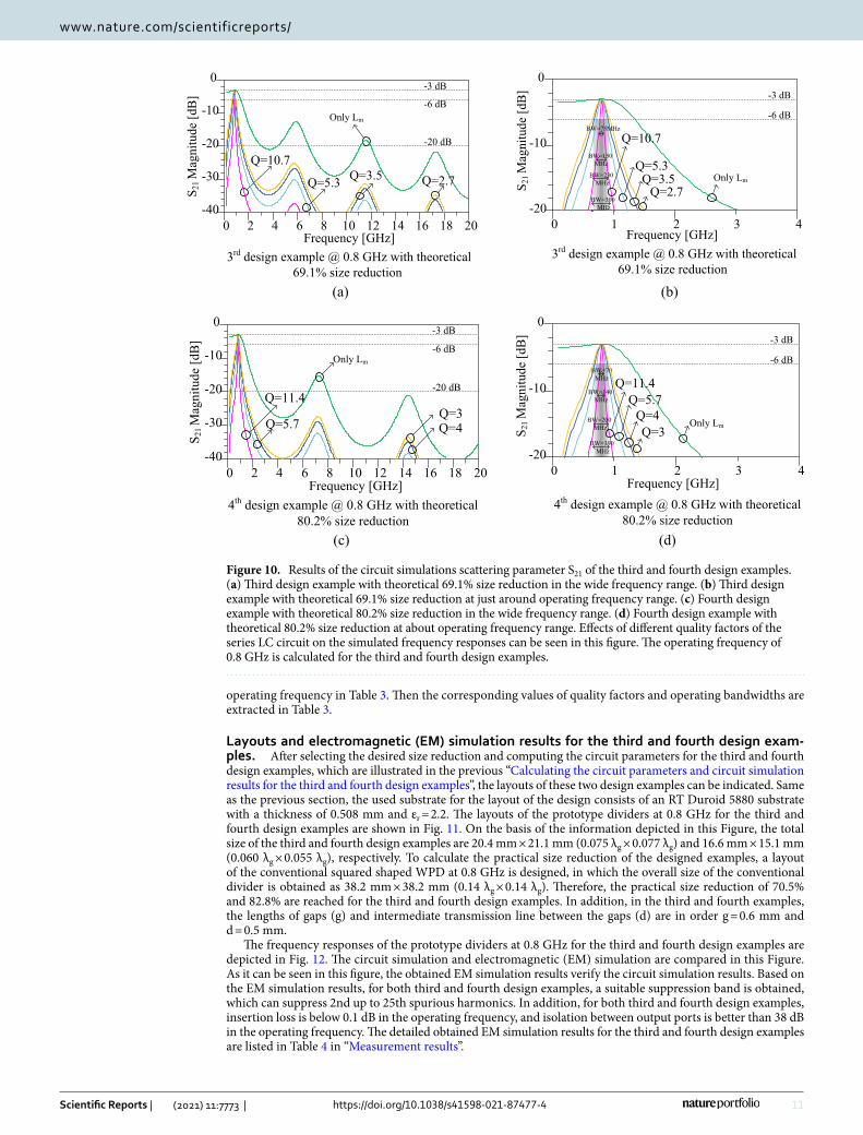
Calculating the circuit parameters and circuit simulation results for the third and fourth design examples. According to Table1, the size reduction values of 69.1% and 80.2% are chosen for the third and fourth design examples, respectively both at 0.8 GHz. The circuit parameters for the third and fourth design examples can be determined with the use of the assumed values of size reduction and operating frequency. As information is given in Table 1, the values of Lm should be equal to 8.8 nH and 9.8 nH for 69.1% and 80.2% size reduction values, respectively. The next steps of the design procedures are done similarly to the first and second design examples, which are explained in “Calculating the circuit parameters and circuit simulation results for the first and second design examples”. The results of the circuit simulations for the third and fourth design exam-ples at 0.8 GHz are illustrated in Fig. 10. In addition, the effects of the series L0C0 circuit with different quality factors on the simulated frequency responses of the presented design examples are demonstrated in this figure. Hence, by increasing the quality factor, the bandwidth decreases while the stopband increases. In other words, by increasing the quality factor more harmonics can be suppressed.
In the next step, the values of L0 and C0 should be determined based on the desired harmonic suppression and operating bandwidth of the WPD. Different values of L0 and C0 combinations are considered for 0.8 GHz
Figure 9. Frequency responses of the prototype dividers at 2.4 GHz for the (a) first design example with theoretical 55.5% size reduction and (b) second design example with theoretical 69.1% size reduction.
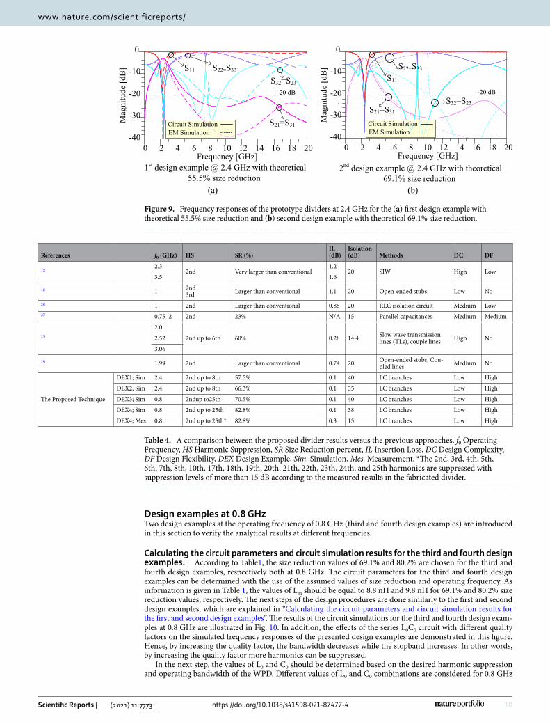
Table 4. A comparison between the proposed divider results versus the previous approaches. f0 Operating Frequency, HS Harmonic Suppression, SR Size Reduction percent, IL Insertion Loss, DC Design Complexity, DF Design Flexibility, DEX Design Example, Sim. Simulation, Mes. Measurement. *The 2nd, 3rd, 4th, 5th, 6th, 7th, 8th, 10th, 17th, 18th, 19th, 20th, 21th, 22th, 23th, 24th, and 25th harmonics are suppressed with suppression levels of more than 15 dB according to the measured results in the fabricated divider.
References f0 (GHz) HS SR (%)IL (dB)
Isolation (dB) Methods DC DF
152.3
2nd Very larger than conventional1.2
20 SIW High Low3.5 1.6
16 1 2nd3rd Larger than conventional 1.1 20 Open-ended stubs Low No
26 1 2nd Larger than conventional 0.85 20 RLC isolation circuit Medium Low27 0.75–2 2nd 23% N/A 15 Parallel capacitances Medium Medium
23
2.0
2nd up to 6th 60% 0.28 14.4 Slow wave transmission lines (TLs), couple lines High No2.52
3.06
29 1.99 2nd Larger than conventional 0.74 20 Open-ended stubs, Cou-pled lines Medium No
The Proposed Technique
DEX1; Sim 2.4 2nd up to 8th 57.5% 0.1 40 LC branches Low High
DEX2; Sim 2.4 2nd up to 8th 66.3% 0.1 35 LC branches Low High
DEX3; Sim 0.8 2ndup to25th 70.5% 0.1 40 LC branches Low High
DEX4; Sim 0.8 2nd up to 25th 82.8% 0.1 38 LC branches Low High
DEX4; Mes 0.8 2nd up to 25th* 82.8% 0.3 15 LC branches Low High
11
Vol.:(0123456789)
Scientific Reports | (2021) 11:7773 | https://doi.org/10.1038/s41598-021-87477-4
www.nature.com/scientificreports/
operating frequency in Table 3. Then the corresponding values of quality factors and operating bandwidths are extracted in Table 3.
Layouts and electromagnetic (EM) simulation results for the third and fourth design exam-ples. After selecting the desired size reduction and computing the circuit parameters for the third and fourth design examples, which are illustrated in the previous “Calculating the circuit parameters and circuit simulation results for the third and fourth design examples”, the layouts of these two design examples can be indicated. Same as the previous section, the used substrate for the layout of the design consists of an RT Duroid 5880 substrate with a thickness of 0.508 mm and εr = 2.2. The layouts of the prototype dividers at 0.8 GHz for the third and fourth design examples are shown in Fig. 11. On the basis of the information depicted in this Figure, the total size of the third and fourth design examples are 20.4 mm × 21.1 mm (0.075 λg × 0.077 λg) and 16.6 mm × 15.1 mm (0.060 λg × 0.055 λg), respectively. To calculate the practical size reduction of the designed examples, a layout of the conventional squared shaped WPD at 0.8 GHz is designed, in which the overall size of the conventional divider is obtained as 38.2 mm × 38.2 mm (0.14 λg × 0.14 λg). Therefore, the practical size reduction of 70.5% and 82.8% are reached for the third and fourth design examples. In addition, in the third and fourth examples, the lengths of gaps (g) and intermediate transmission line between the gaps (d) are in order g = 0.6 mm and d = 0.5 mm.
The frequency responses of the prototype dividers at 0.8 GHz for the third and fourth design examples are depicted in Fig. 12. The circuit simulation and electromagnetic (EM) simulation are compared in this Figure. As it can be seen in this figure, the obtained EM simulation results verify the circuit simulation results. Based on the EM simulation results, for both third and fourth design examples, a suitable suppression band is obtained, which can suppress 2nd up to 25th spurious harmonics. In addition, for both third and fourth design examples, insertion loss is below 0.1 dB in the operating frequency, and isolation between output ports is better than 38 dB in the operating frequency. The detailed obtained EM simulation results for the third and fourth design examples are listed in Table 4 in “Measurement results”.
Figure 10. Results of the circuit simulations scattering parameter S21 of the third and fourth design examples. (a) Third design example with theoretical 69.1% size reduction in the wide frequency range. (b) Third design example with theoretical 69.1% size reduction at just around operating frequency range. (c) Fourth design example with theoretical 80.2% size reduction in the wide frequency range. (d) Fourth design example with theoretical 80.2% size reduction at about operating frequency range. Effects of different quality factors of the series LC circuit on the simulated frequency responses can be seen in this figure. The operating frequency of 0.8 GHz is calculated for the third and fourth design examples.

12
Vol:.(1234567890)
Scientific Reports | (2021) 11:7773 | https://doi.org/10.1038/s41598-021-87477-4
www.nature.com/scientificreports/
Measurement resultsTo verify the simulation and analyses results, the fourth design example with theoretical 80.2% and practical 82.8% size reduction at the operating frequency of 0.8 GHz is implemented on the high-frequency substrate with the specifications of RT Duroid 5880 with a thickness of 0.508 mm (20 mil) and εr = 2.2. Figure 13 com-pares experimental results with the EM simulation results. The fabricated divider is measured using Agilent E8362B Network Analyzer. The measurement is set up to 20 GHz frequency to clarify the harmonic suppression performance.
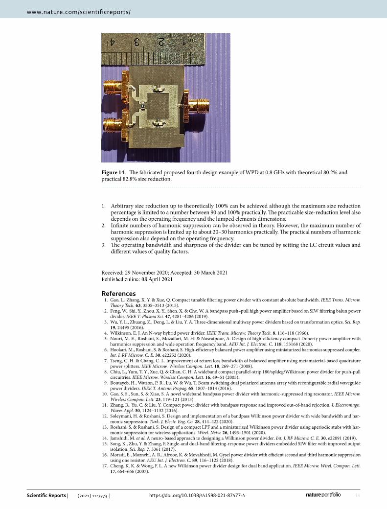
The measured results show that the proposed divider can practically operate at 0.7 GHz up to 0.95 GHz, which indicates 250 MHz operating bandwidth. The minimum insertion loss is 0.3 dB at this bandwidth. As is observed, the proposed divider can work properly at 0.8 GHz frequency with desirable specifications. Moreover, according to the measured results, the isolation between the output ports, input return loss, and output return loss is 15 dB, 14 dB and 22 dB, respectively. A proper suppression band is obtained for the proposed divider with a suppression level of more than 20 dB. The 2nd, 3rd, 4th, 5th, 6th, 7th, 8th, 10th, 17th, 18th, 19th, 20th, 21th, 22th, 23th, 24th, and 25th harmonics are suppressed with suppression levels of more than 15 dB, according to the measured results. The fabricated proposed WPD is shown in Fig. 14.
Table 4 provides information about the proposed divider results compared to the previous filtering dividers. Design Flexibility (DF) in this table means that the main parameters of the divider, such as size reduction, har-monic suppression, and bandwidth can be changed to the desired values. According to the information provided in Table 4, the proposed hybrid method is capable of designing a WPD with high design flexibility, low design complexity (DC), compact size, and high levels of harmonic suppression. Therefore, this innovative modification can contribute to considerable improvements in the design of the next generation of microwave components.
Figure 11. Layouts of the prototype dividers at 0.8 GHz for the (a) third design example with theoretical 69.1% size reduction and (b) fourth design example with theoretical 80.2% size reduction (All dimensions are in mm).
Figure 12. Frequency responses of the prototype WPDs at 0.8 GHz for the (a) third design example with theoretical 69.1% size reduction and (b) fourth design example with theoretical 80.2% size reduction.

13
Vol.:(0123456789)
Scientific Reports | (2021) 11:7773 | https://doi.org/10.1038/s41598-021-87477-4
www.nature.com/scientificreports/
ConclusionsAn innovative hybrid technique for size reduction and performance improvement of a microstrip WPD has been conducted and demonstrated in this paper. In this method, microstrip lines in the WPD are replaced by the proposed LC branches. This replacement leads to extreme size reduction, filtering response, and improving performance. To assess the effectiveness of the proposed approach, four WPDs have been designed and simulated by amending their branch lines. This alteration in branches breeds an enormous size reduction and harmonic suppression in the dividers. In order to survey the practical performance of the designed WPDs, one of them was fabricated and its excremental results were measured. The results demonstrated the capability and efficiency of the introduced method to improve such components. Accordingly, 100% size reduction and an infinite number of harmonics suppression are reached theoretically. However, due to lumped element lengths, the theoretical size reduction can be mildly affected in practice, especially in high frequencies. In addition, folding and bend-ing the microstrip lines may have slight effects on the theoretical values. Consequently, the proposed technique dramatically improves the efficiency and size of such components and provides new fields in the development of many other microstrip components, such as microstrip resonators, filters, diplexers, matching networks, couplers, power amplifiers, and the other types of dividers.
The following results can be concluded from the proposed method.
Figure 13. Frequency responses of the fabricated fourth design example at 0.8 GHz with theoretical 80.2% and practical 82.8% size reduction. (a) The S21 and S11 scattering parameters in the wide frequency range. (b) The S32 and S22 scattering parameters in the wide frequency range. (c) The S21 scattering parameter at about operating frequency range.
14
Vol:.(1234567890)
Scientific Reports | (2021) 11:7773 | https://doi.org/10.1038/s41598-021-87477-4
www.nature.com/scientificreports/
1. Arbitrary size reduction up to theoretically 100% can be achieved although the maximum size reduction percentage is limited to a number between 90 and 100% practically. The practicable size-reduction level also depends on the operating frequency and the lumped elements dimensions.
2. Infinite numbers of harmonic suppression can be observed in theory. However, the maximum number of harmonic suppression is limited up to about 20–30 harmonics practically. The practical numbers of harmonic suppression also depend on the operating frequency.
3. The operating bandwidth and sharpness of the divider can be tuned by setting the LC circuit values and different values of quality factors.
Received: 29 November 2020; Accepted: 30 March 2021
References 1. Gao, L., Zhang, X. Y. & Xue, Q. Compact tunable filtering power divider with constant absolute bandwidth. IEEE Trans. Microw.
Theory Tech. 63, 3505–3513 (2015). 2. Feng, W., Shi, Y., Zhou, X. Y., Shen, X. & Che, W. A bandpass push–pull high power amplifier based on SIW filtering balun power
divider. IEEE T. Plasma Sci. 47, 4281–4286 (2019). 3. Wu, Y. L., Zhuang, Z., Deng, L. & Liu, Y. A. Three-dimensional multiway power dividers based on transformation optics. Sci. Rep.
19, 24495 (2016). 4. Wilkinson, E. J. An N-way hybrid power divider. IEEE Trans. Microw. Theory Tech. 8, 116–118 (1960). 5. Nouri, M. E., Roshani, S., Mozaffari, M. H. & Nosratpour, A. Design of high-efficiency compact Doherty power amplifier with
harmonics suppression and wide operation frequency band. AEU Int. J. Electron. C. 118, 153168 (2020). 6. Hookari, M., Roshani, S. & Roshani, S. High-efficiency balanced power amplifier using miniaturized harmonics suppressed coupler.
Int. J. RF Microw. C. E. 30, e22252 (2020). 7. Tseng, C. H. & Chang, C. L. Improvement of return loss bandwidth of balanced amplifier using metamaterial-based quadrature
power splitters. IEEE Microw. Wireless Compon. Lett. 18, 269–271 (2008). 8. Chiu, L., Yum, T. Y., Xue, Q. & Chan, C. H. A wideband compact parallel-strip 180/spldeg/Wilkinson power divider for push-pull
circuitries. IEEE Microw. Wireless Compon. Lett. 16, 49–51 (2005). 9. Boutayeb, H., Watson, P. R., Lu, W. & Wu, T. Beam switching dual polarized antenna array with reconfigurable radial waveguide
power dividers. IEEE T. Antenn Propag. 65, 1807–1814 (2016). 10. Gao, S. S., Sun, S. & Xiao, S. A novel wideband bandpass power divider with harmonic-suppressed ring resonator. IEEE Microw.
Wireless Compon. Lett. 23, 119–121 (2013). 11. Zhang, B., Yu, C. & Liu, Y. Compact power divider with bandpass response and improved out-of-band rejection. J. Electromagn.
Waves Appl. 30, 1124–1132 (2016). 12. Soleymani, H. & Roshani, S. Design and implementation of a bandpass Wilkinson power divider with wide bandwidth and har-
monic suppression. Turk. J. Electr. Eng. Co. 28, 414–422 (2020). 13. Roshani, S. & Roshani, S. Design of a compact LPF and a miniaturized Wilkinson power divider using aperiodic stubs with har-
monic suppression for wireless applications. Wirel. Netw. 26, 1493–1501 (2020). 14. Jamshidi, M. et al. A neuro-based approach to designing a Wilkinson power divider. Int. J. RF Microw. C. E. 30, e22091 (2019). 15. Song, K., Zhu, Y. & Zhang, F. Single-and dual-band filtering-response power dividers embedded SIW filter with improved output
isolation. Sci. Rep. 7, 3361 (2017). 16. Moradi, E., Moznebi, A. R., Afrooz, K. & Movahhedi, M. Gysel power divider with efficient second and third harmonic suppression
using one resistor. AEU Int. J. Electron. C. 89, 116–1122 (2018). 17. Cheng, K. K. & Wong, F. L. A new Wilkinson power divider design for dual band application. IEEE Microw. Wirel. Compon. Lett.
17, 664–666 (2007).
Figure 14. The fabricated proposed fourth design example of WPD at 0.8 GHz with theoretical 80.2% and practical 82.8% size reduction.

15
Vol.:(0123456789)
Scientific Reports | (2021) 11:7773 | https://doi.org/10.1038/s41598-021-87477-4
www.nature.com/scientificreports/
18. Cheng, K. K. & Law, C. A novel approach to the design and implementation of dual-band power divider. IEEE Trans. Microw. Theory Tech. 56, 487–492 (2008).
19. Cheng, K. K. & Ip, W. C. A novel power divider design with enhanced spurious suppression and simple structure. IEEE Trans. Microw. Theory Tech. 58, 3903–3908 (2010).
20. Amin, M., Ramzan, R. & Siddiqui, O. Slow wave applications of electromagnetically induced transparency in microstrip resonator. Sci. Rep. 8, 2357 (2018).
21. Wang, Y., Zhang, X. Y., Liu, F. X. & Lee, J. C. A compact bandpass Wilkinson power divider with ultra-wide band harmonic sup-pression. IEEE Microw. Wirel. Compon. Lett. 27, 888–890 (2017).
22. Chen, M. T. & Tang, C. W. Design of the filtering power divider with a wide passband and stopband. IEEE Microw. Wirel. Compon. Lett. 28, 570–572 (2018).
23. Song, K., Hu, S., Zhang, F., Zhu, Y. & Fan, Y. Compact dual-band filtering-response power divider with high in-band frequency selectivity. Microelectron. J. 69, 73–76 (2017).
24. Barakat, R., Nerguizian, V., Hammou, D. & Tatu, S. O. Modified ring power divider using stepped-impedance resonator. J. Microw. Optoelectron. Electromagn. Appl. 19, 26–38 (2020).
25. Jamshidi, M. B., Lalbakhsh, A., Mohamadzade, B., Siahkamari, H. & Mousavi, S. M. A novel neural-based approach for design of microstrip filters. AEU Int. J. Electron. C. 110, 152847 (2019).
26. Chao, S. F. & Li, Y. R. Miniature filtering power divider with increased isolation bandwidth. Electron. Lett. 50, 608–610 (2014). 27. Chen, A., Zhuang, Y., Zhou, J., Huang, Y. & Xing, L. Design of a broadband Wilkinson power divider with wide range tunable
bandwidths by adding a pair of capacitors. IEEE Trans. Circuits Syst. II(66), 567–571 (2018). 28. Wang, Y., Xiao, F., Cao, Y., Zhang, Y. & Tang, X. Novel wideband microstrip filtering power divider using multiple resistors for
port isolation. IEEE Access. 7, 61868–61873 (2019). 29. Liu, F. X., Wang, Y., Zhang, X. Y., Quan, C. H. & Lee, J. C. A size-reduced tri-band Gysel power divider with ultra-wideband
harmonics suppression performance. IEEE Access. 6, 34198–34205 (2018).
AcknowledgementThis research has been supported by the Ministry of Education, Youth and Sports of the Czech Republic under the project OP VVV Electrical Engineering Technologies with High-Level of Embedded Intelligence CZ.02.1.01/0.0/0.0/18_069/0009855. This paper is dedicated to the memory of our dear friend and colleague Dr. Arash Zarinitabar from Islamic Azad University, Kermanshah, Iran, who passed away on February 21, 2021.
Author contributionsSO.R. contributed to the conception of the idea. M.B.J., SA.R., and SO.R. developed the main idea for useable applications and designed the different structures. M.B.J., SA.R. and SO.R. performed the simulations. M.B.J., J.T., and Z.P. performed the device fabrication, measurements, and wrote the article with support from SA.R. and SO.R. The team was directed and led by Z.P. All authors reviewed the manuscript.
Competing interests The authors declare no competing interests.
Additional informationCorrespondence and requests for materials should be addressed to S.R.
Reprints and permissions information is available at www.nature.com/reprints.
Publisher’s note Springer Nature remains neutral with regard to jurisdictional claims in published maps and institutional affiliations.
Open Access This article is licensed under a Creative Commons Attribution 4.0 International License, which permits use, sharing, adaptation, distribution and reproduction in any medium or
format, as long as you give appropriate credit to the original author(s) and the source, provide a link to the Creative Commons licence, and indicate if changes were made. The images or other third party material in this article are included in the article’s Creative Commons licence, unless indicated otherwise in a credit line to the material. If material is not included in the article’s Creative Commons licence and your intended use is not permitted by statutory regulation or exceeds the permitted use, you will need to obtain permission directly from the copyright holder. To view a copy of this licence, visit http:// creat iveco mmons. org/ licen ses/ by/4. 0/.
© The Author(s) 2021