sir c.r.reddy college of engineering eluru …sir c r reddy college of engineering 6 department of...
TRANSCRIPT

Sir C R Reddy College of Engineering Department of ECE 1
SIR C.R.REDDY COLLEGE OF ENGINEERING
ELURU-534 007
Department of Electronics and Communications
MICROWAVE AND ANTENNAS Lab Manual (EC-425)
For IV / IV B.E (ECE), II - Semester
SIR C.R.REDDY COLLEGE OF ENGINEERING
ELURU-534 007

Sir C R Reddy College of Engineering Department of ECE 2
SIR C.R.REDDY COLLEGE OF ENGINEERING
ELURU-534007
Dept. of ECE
MICROWAVE AND ANTENNAS LAB
LIST OF EXPERIMENTS (PRESCRIBED)
1. STUDY OF GUNN DIODE CHARACTERISTICS
2. STUDY OF REFLEX KLYSTRON CHARACTERISTICS
3. SETUP OF OPTICAL FIBER ANALOG LINK
4. SETTING UP A FIBRE OPTIC DIGITAL LINK
5. STUDY OF LOSSES IN OPTICAL FIBER
6. RADIATION PATTERN OF THREE ELEMENT YAGI-UDA ANTENNA.
7. RADIATION PATTERN OF A DIPOLE ANTENNA.
8. STUDY OF LOG-PERIODIC ANTENNA
9. SPECTRUM ANALYZER : HORMONICS OF SINE WAVE
10.SPECTRUM ANALYZER : HORMONICS OF SQUARE WAVE
11. MICRO STRIP DIRECTIONAL COUPLER

Sir C R Reddy College of Engineering Department of ECE 3
1. STUDY OF GUNN DIODE CHARACTERISTICS AIM: To study the V-I Characteristics and Frequency Vs Power Characteristics of the Gunn Diode. EQUIPMENT REQUIRED:
1. Gunn power supply 2. Gunn diode mount 3. PIN modulator 4. Isolator with matched load 5. variable attenuator 6. Detector Mount 7. Power Meter.
THEORY:
Transferred electron devices are two terminal semi conductor devices which have wide applications as sources of Continues Wave and pulsed power at microwave frequencies because of their bulk negative resistance behavior, these devices are ideally suited for use in low noise sources such as local oscillators. PROCEDURE:
1. Assemble the test bench as shown in figure. 2. Switch on the Gunn power supply, check the voltage knob is in zero position,
connect the Gunn diode bias supply and PIN modulator supply. 3. Slowly increase the Gunn bias supply in steps of 0.5 Volts and for each increment
observe the Gunn current and plot the V-I characteristics. 4. Set the Gunn Bias voltage to 9.0 Volts, by changing Micrometer measure the power
using power meter and find the corresponding frequency for each micrometer reading. 5. Plot the graph frequency Vs power for different modes.

Sir C R Reddy College of Engineering Department of ECE 4
PRECAUTIONS: 1. Do not apply the Gunn bias voltage greater than 12.0 Volts. 2. Keep the connections without gaps. RESULT: The Threshold voltage of the Gunn Diode found as ……………….

Sir C R Reddy College of Engineering Department of ECE 5
VIVA QUESTIONS;
1. Why transfer electronic devices are called Bulk effect devices? 2. Why GaAs is preferred for the construction of TEDs? 3. What is Gunn effect 4. Why Gunn diodes are called TEDs 5. What is negative resistance property? 6. What are the different modes of operations in Gunn Diodes? 7. What is two-valley model theory? 8. What is the significance of RWH theory in Gunn Diodes? 9. What is LSA Diode? 10. What is the Significance of Frequency length (nl) product? 11. What are the applications of Gunn Diode? 12. What is PIN modulator?

Sir C R Reddy College of Engineering Department of ECE 6
2. STUDY OF REFLEX KLYSTRON CHARACTERISTICS AIM:- To study the dependence of microwave power output and frequency on the Repeller voltage. EQUIPMENTS REQUIRED:- Klystron power supply 5. Variable attenuator Klystron mounts 6. Frequency meter Reflex klystron 7. Detector mount Isolator 8. VSWR Meter and C.R.O THEORY: Reflex Klystron is a single cavity Resonator Klystron; it is a low power source delivering 10 to 100 mW output in the frequency range of 1 to 30GHz with an efficiency of 30%. PROCEDURE:-
1. Assemble the test bench as shown in the figure. 2. Beam voltage knob should be at min position. 3. Adjust the Repeller voltage to 70 to 100 volts and beam voltage to 270 volts and beam
current should be around 5 to 30mA, modulation is set to AM. 4. Energize the Klystron to get maximum power on the VSWR meter. 5. Observe the perfect square wave on the CRO. 6. Measure the output power (VSWR meter reading) and frequency (by tuning the
frequency meter) for different values of Repeller voltage (Multimeter reading) from 30V to 160V.
7. Plot Repeller voltage Vs power and Repeller Voltage Vs frequency. TABULAR FORM:-
Repeller voltage Volts
Power in dB (VSWR Meter)
Frequency GHz (frequency meter)
MODEL GRAPH (MODE DIAGRAM):

Sir C R Reddy College of Engineering Department of ECE 7
PRECAUTIONS:-
1. Do not look into the transmitting horn. 2. Keep the cooling fan towards the Klystron tube. 3. Never keep the Repeller Voltage to zero volts.
RESULT:- The Mode Diagram of Repeller Klystron i.e, frequency Vs Repeller voltage and power Vs Repeller voltage were plotted. Viva Questions:
1. What is Bunching? 2. Where the Bunching occurs in Klystrons? 3. What is the operation principal of Reflex Klystron? 4. What is the Density modulation? 5. Klystron type tubes can operate at high frequencies the triodes. Why? 6. What is the effect of increasing number of cavities in Klystron? 7. What is linier Frequency modulation in Klystrons? 8. What is beam loading? 9. What is beam-coupling co-efficient? 10. What is the optimum value of Bunching parameter? 11. What is the relation between Anode voltage and Repeller voltage? 12. Why Repeller electrode is maintained at high negative potential? 13. Draw the equivalent circuit of Reflex Klystron? 14. What is the efficiency of Reflex Klystron? 15. Why square wave modulation of the source is preferred?

Sir C R Reddy College of Engineering Department of ECE 8
3. SETUP OF OPTICAL FIBER ANALOG LINK AIM: The objective of this experiment is to study 950nm Fiber Optic Analog Link. In this experiment you will study the relationship between the input signal and the received signal. THEORY: Fiber optic links can be used for transmission of digital and analog signal. Basically a Fiber optic link contains three main elements, a transmitter, an Optical Fiber and a Receiver. The transmitter module takes the input signal in electrical form and transforms it into Optical (light) energy containing the same information. The Optical fiber is the medium, which carries this energy to the receiver. At the receiver, the light is converted back into electrical form with the same pattern as originally fed to the transmitter. EQUIPMENTS: Power supply Kit-1 and Kit-2 20 MHz Dual channel Oscilloscope 1 Meter Fiber Cable PROCEDURE:
1. Refer the fig and make the following connections. 2. Slightly unscrew the cap of IR LED SFH 450V (950nm) from Kit-1. Do not remove the
cap from the connector. Once the connecter is lessened, insert the fiber into the cap and assure that the fiber is properly fixed. Now tighten the cap by screwing it back.
3. Connect the power supply cables with proper polarities to Kit-1 and Kit-2. While connecting this, ensure that the power supply is OFF.
4. Connect the 1 KHz on board sine wave to the AMP I/P posts in Kit-1 to feed the Analog signal to the Amplifier.
5. Keep the signal generator in sine wave mode and select the frequency of 1 KHz with amplitude of 1V p-p.
6. Switch on the power supply. 7. Check the output of the Amplifier at the post AMP O/P in KIT-1. 8. Now rotate the Optical fiber control pot P1 located below power supply connecter in
Kit1 in Anti-Clock wise direction. This ensures minimum current flow through LED. 9. Short the following posts in Kit-1. With the links provided.
+9V and +9V – This ensures supply to the transmitter. AMP O/P and transmitter input.
10. Connect the other end of the fiber to detector SFH 250V (Analog Detector) in Kin-2 very carefully as per the instructions in step-1.
11. Ensure the jumper located just above IC UI in Kit-2 is shorted to Pins 2 and 3. Shorting of the jumper allows the connection of PIN Diode to trans-impedance amplifier stage.
12. Observe the output signal from the detector at detector output post on CRO by adjusting the Optical Power control Pot P1 in Kit-1 and you should get the reproduction of the original transmitted signal.

Sir C R Reddy College of Engineering Department of ECE 9
NOTE: Same output signal is available at post AC O/P in Kit-2 with out any DC component.
13. To measure the Analog Band Width of the Link, Keep the same connections and vary the Frequency of the input signal from 100 Hz onwards. Measure the Amplitude of the Received signal for each frequency reading.
14. Plot a graph of Gain/ Frequency. Measure the frequency range for witch the response is
flat. MODEL GRAPH:

Sir C R Reddy College of Engineering Department of ECE 10
RESULT: studied the relationship between the input signal and the received signal. VIVA QUESTIONS:
1. What are the advantages of Optical Fibers over Copper Medium? 2. How the light wave will propagate through the Optical Fiber. 3. Define Refractive Index. 4. Define Brewster’s angle. 5. Explain about analog link Setup using OFC. 6. Explain the Principle of Photo Diode. 7. Explain the Principle of Photo Detector. 8. What are the different types of fibers?

Sir C R Reddy College of Engineering Department of ECE 11
4. SETTING UP A FIBER OPTIC DIGITAL LINK AIM: The Objective of this experiment is to study 950 nm fiber optic digital link. Here you will study how digital signal can be transmitted over fiber cable and reproduce at the receiver end. THEORY: In the experiment no.1, we have seen how analog signal can be transmitted and received using LED, fiber and detector. The same LED, fiber and detector can be configured for the digital applications to transmit binary data over fiber. Thus basic elements of the link remain same even for digital applications. Transmitter: LED, digital, DC coupled transmitters are one of the most popular variety due to their ease of fabrication. We have used a standard TTL gate to drive a NPN-transistor, Which modulates the LED SFH 40V Source (turns it ON or OFF). Receiver: There are various methods to configure detectors to extract digital data. Usually detectors are of linear nature. We have used a photo detector having TTL type output. Usually it consists of PIN photodiode, trans-impedance amplifier and level shifter.
EQUIPMENT:
Power Supply. 20 MHz dual trace oscilloscope 1MHZ function generator 1m fiber cable.
PROCEDURE:
1. Refer fig. And make the following connections. 2. Slightly unscrew the cap of IR LED SFH450V. Do not remove the cap from the
connector. Once the cap is loosened, insert the fiber into the cap. A fiber is properly fixed if you get light click. Now tighten the cap by screwing it back.
3. Connect the power chord to the kit and switch on the power supply. 4. Fed the TTL signal of about 1 KHz from the function generator between BUFFER
INPUT and GND posts. Observe the signal at BUFFER OUTPUT POST; it should be same as that of input signal.
5. Short BUFFER OUTPUT and TRANSMITTER INPUT posts with the help of shorting link is provided.
6. Connect the other end of the fiber to detector SFH551V vary carefully as per the instructions in step1.
7. Observe the received signal on CRO at TTL OUTPUT post (tp8). The transmitted signal and received signal are same except of a slight delay in the received signal.
8. Vary the frequency of the input signal and observe the output response. Observe the variation in the duty cycle of the signal and determine the maximum bit rate that can be transmitted on the digital link.

Sir C R Reddy College of Engineering Department of ECE 12
RESULT: Maximum bit rate possible through the given fiber is found as ………………..

Sir C R Reddy College of Engineering Department of ECE 13
5. STUDY OF LOSSES IN OPTICAL FIBER AIM: The objective of this experiment is to measure propagation loss in plastic fiber provided with the lab for different wavelengths of radiation as 950nm,660nm and also to measure the bending loss. EQUIPMENTS: Kit 1, kit2, kit3 and kit4 1 MHz function generator 20MHz dual trace oscilloscope 1&3 meter fiber cable PROCEDURE:
1. Slightly unscrew the cap of IR LEDSFH 450V from kit1. Do not remove the cap from the connector. Once the cap is loosened, insert the fiber into the cap and assure that the fiber is properly fixed. Now tighten the cap by screwing it back.
2. Connect the power supply cable with proper polarity to kit1 and kit2. While connecting this ,ensure that the power supply is OFF.
3. Connect the signal generator between the AMP I/P and GND ports in kit1 to feed the anlog signal to the pre-amplifier.
4. Keep the signal generator in sine wave mode and select the frequency =1KHzwith amplitude=2Vp-p (Max input level is 4Vp-p)
5. Switch on the supply is OFF. 6. Check the output signal of the pre-amplifier at the post AMP O/P in kit 1. 7. Now rotate optical power control pot P1 located below power supply connector in kit1 in
anticlock wise direction . this ensures minimum current flow through LED. 8. Short the following posts in kit1 with the links provided.
+9V and +9V – this ensures supply to the transmitter. Amp o/p and transmitter i/p.
9. Connect the other end of the fiber to the detector SFH 250V in kit2 very carefully as per the instruction in step1.
10. Ensure that the jumper located just above IC U1 in kit2 is shorted to pins2 and 3.shorting of the jumper allows connection of PIN photo diode to the transimpedance amplifier input.
11. Observe the output signal from the detector at AC OUTPUT post in kit 2 on CRO. Adjust optical power control pot P1 in kit1.you should get the reproduction of the original transmitted signal. Also adjust the amplitude of received signal as that of the transmitted one. Mark this amplitude level as V1.
12. Now replace 1 meter fiber by 3 meter fiber without disturbing any of the previous setting in kit1&kit2. Measure the amplitude level at the receiver side again. You will notice that it is less than the previous one. Mark this as V2.
13. If α is the attenuation of the fiber then we have
P1/P2 = V1/V2=
Where i. α = nepers/meter.
ii. L1= fiber length for V1.
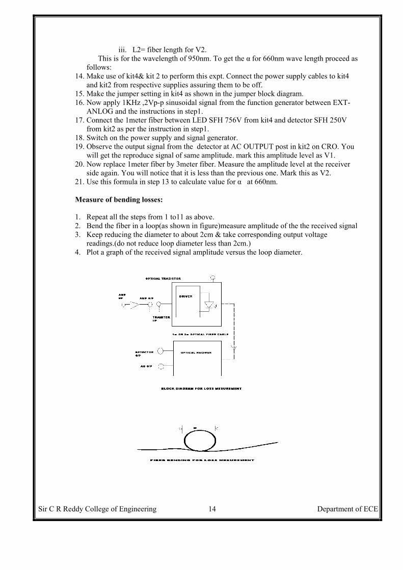
Sir C R Reddy College of Engineering Department of ECE 14
iii. L2= fiber length for V2. This is for the wavelength of 950nm. To get the α for 660nm wave length proceed as
follows: 14. Make use of kit4& kit 2 to perform this expt. Connect the power supply cables to kit4
and kit2 from respective supplies assuring them to be off. 15. Make the jumper setting in kit4 as shown in the jumper block diagram. 16. Now apply 1KHz ,2Vp-p sinusoidal signal from the function generator between EXT-
ANLOG and the instructions in step1. 17. Connect the 1meter fiber between LED SFH 756V from kit4 and detector SFH 250V
from kit2 as per the instruction in step1. 18. Switch on the power supply and signal generator. 19. Observe the output signal from the detector at AC OUTPUT post in kit2 on CRO. You
will get the reproduce signal of same amplitude. mark this amplitude level as V1. 20. Now replace 1meter fiber by 3meter fiber. Measure the amplitude level at the receiver
side again. You will notice that it is less than the previous one. Mark this as V2. 21. Use this formula in step 13 to calculate value for α at 660nm. Measure of bending losses:
1. Repeat all the steps from 1 to11 as above. 2. Bend the fiber in a loop(as shown in figure)measure amplitude of the the received signal 3. Keep reducing the diameter to about 2cm & take corresponding output voltage
readings.(do not reduce loop diameter less than 2cm.) 4. Plot a graph of the received signal amplitude versus the loop diameter.

Sir C R Reddy College of Engineering Department of ECE 15
RESULT: Bending losses of the given fiber studied.

Sir C R Reddy College of Engineering Department of ECE 16
6. RADIATION PATTERN OF THREE ELEMENT YAGI-UDA ANTENNA. AIM: To plot the polar plot for three element Yagi-Uda antenna. APPARATUS: S9990 microstrip antenna trainer polar positioner & fixed clamp two Yagi-Uda antennas S1189 transmitter/receiver THEORY: Receiver: The Receiver is used for the measurement of RF signal level with a high accuracy and repeatability. Facility is provided for obtaining the Polar Diagram of the Antennas. Frequency from 850 MHz to 1300 MHz can be measured. For obtaining the Polar Diagram, the Receiving Antenna is rotated by 5 degrees and the readings are stored in the memory of the unit. SPECIFICATIONS: Frequency Range: 850 MHz to 1300MHz freq range Input Impedance: 50ohms nominal Level Resolution: .1dB resolution Level Range: >65 dB measurement range. Level Accuracy: +-3dB typ accy at 50ohms Level Array: Array of 72 points is provided for storing Polar dBuV readings. Display: LCD Display 16 Character x 2 Line Power: 230V AC rms + 10%, 50Hz TRANSMITTER GENERATOR: Transmitting source to drive the transmitting antenna. 850 MHz to 1300 MHz variable source with a nominal output of >105 dBuV at 50ohms, to obtain the Polar Plot of the antenna under test. 5 digit LED display of Frequency counter displays Frequency of Output. Acc. 100 PPM.

Sir C R Reddy College of Engineering Department of ECE 17
BLOCK DIAGRAM: PROCEDURE: connect the S-1189 as shown in the fig. above Mount the transmitter antenna on the stand connect it to the S-9990 transmitter O/P as shown. Mount the receiver antenna on the positioner and connect it to the S-9990 receiver to the I/P as shown. Set the transmitter frequency to 900 MHz. keep the antenna in the horizontal direction. Rotate the antenna in the steps of 5o manually. Note down the readings in table given below upto 360o. Plot the polar plot based on the values obtained. TABLE: RESULT:
Radiation pattern of the Yagi-Uda antenna is plotted.
S. No Angle in degrees Power level in dB µV

Sir C R Reddy College of Engineering Department of ECE 18
7. RADIATION PATTERN OF A DIPOLE ANTENNA. AIM: To plot the radiation pattern of the Dipole antenna. APPARATUS: S1189 transmitter/receiver S 9990 antenna trainer Two Dipole antennas THEORY: Receiver: The Receiver is used for the measurement of RF signal level with a high accuracy and repeatability. Facility is provided for obtaining the Polar Diagram of the Antennas. Frequency from 850 MHz to 1300 MHz can be measured. For obtaining the Polar Diagram, the Receiving Antenna is rotated by 5 degrees and the readings are stored in the memory of the unit. SPECIFICATIONS: Frequency Range: 850 MHz to 1300MHz freq range Input Impedance: 50ohms nominal Level Resolution: .1dB resolution Level Range: >65 dB measurement range. Level Accuracy: +-3dB typ accy at 50ohms Level Array: Array of 72 points is provided for storing Polar dBuV readings. Display: LCD Display 16 Character x 2 Line Power: 230V AC rms + 10%, 50Hz TRANSMITTER GENERATOR: Transmitting source to drive the transmitting antenna. 850 MHz to 1300 MHz variable source with a nominal output of >105 dBuV at 50ohms, to obtain the Polar Plot of the antenna under test. 5 digit LED display of Frequency counter displays Frequency of Output. Acc. 100 PPM.

Sir C R Reddy College of Engineering Department of ECE 19
BLOCK DIAGRAM: PROCEDURE: connect the S-1189 as shown in the fig. above Mount the transmitter antenna on the stand connect it to the S-9990 transmitter O/P as shown. Mount the receiver antenna on the positioner and connect it to the S-9990 receiver to the I / P as shown. Set the transmitter frequency to 900 MHz. keep the antenna in the horizontal direction. Rotate the antenna in the steps of 5o manually. Note down the readings in table given below upto 360o. Plot the polar plot based on the values obtained. RESULT: Radiation pattern of the Dipole antenna is plotted.

Sir C R Reddy College of Engineering Department of ECE 20
8. STUDY OF LOG-PERIODIC ANTENNA
AIM:
a) To plot the radiation pattern of Log-periodic antenna in E &H planes on Log & linear scales on polar and Cartesian plots.
b) To measure the beam width (-3db) front to back ratio, side lobe level and its angular position, plane of polarization, directivity & gain of the log-periodic antenna.
c) To study antenna resonance and measure VSWR, impedance and impedance bandwidth using RLB and adjust the antenna dimensions for resonance. EQUIPMENT REQUIRED:
1. Antenna transmitter, receiver and stepper motor controller. 2. Dipole antenna, Log-periodic antenna. 3. Antenna Tripod and stepper pod with connecting cables, Polarization connector.
PROCEDURE: Radiation pattern of Log-periodic antenna in E &H planes:
1. Connect the dipole antenna to the input and set the transmitter frequency to 600 MHZ. Keep the antenna in horizontal direction. Adjust the dipole for resonance at 600 MHZ.
2. Now connect the Log-periodic antenna to the stepper tripod and set the receiver to 600 MHZ.
3. Adjust Log-periodic elements as per figure given below, 4. Set the distance between antennas to be around 1m. 5. Take the level reading of receiver and see the reading is not more than 70dB after which
attenuators need to be pressed. 6. Now rotate the Log- periodic antenna around its axis in steps of 5 degrees using stepper
motor controller. Take the level readings of each step and note down. 7. Plot the readings on polar or Cartesian plane with log/linear scales on the graph papers
provided at the back of the manual. 8. This plot with dipole & Log-periodic in horizontal plane shall form an E-plane plot. 9. Now without disturbing the setup – rotate the dipole antenna at receiver from horizontal
to vertical plane by using a polarization connector. 10. Similarly turn the Log-periodic to vertical plane. Now rotate the Log-periodic antenna
around its axis in steps of degrees using stepper motor controller. Take the level readings of receiver at each step and note down.
11. This plot shall constitute the H-plane plot of the Log-periodic antenna Beam width (-3db) front to back ratio, side lobe level and its angular position, plane of polarization, directivity & gain.
1. From the E –plane radiation patterns have drawn in experiment A find the following. 2. From the plot measure the angle where the 0dB reference is there. This shall also be the
direction of main lobe or bore sight direction. 3. Measure the angle when this reading is -3dB on its either side. 4. The difference between the angular position and level can be inferred from the plot.

Sir C R Reddy College of Engineering Department of ECE 21
5. Side lobe’s angular position and level can be inferred from the plot. 6. The front to back can be inferred from difference in levels in dB from bore sight
direction and direction diametrically opposite to it. 7. Find the plane of polarization of the Log-periodic by comparing to dipole. 8. The directivity can be found by measuring E-plane and H-plane beam-widths using the
relation as explained earlier. 9. The gain of Log-periodic antenna in dB can be found by subtracting the Log-periodic
antenna bore sight receiver reading with a dipole antenna connected in place. But ensure that dipole is replaced in same polarization plane and has been tuned at that frequency.
Antenna resonance and VSWR, impedance and impedance bandwidth
1. Connect the return loss bridge to the transmitter tripod through the TX connector. 2. Connect the Log-periodic antenna to the RLB at the ANT connector. 3. Connect the receiver to the RLB at the RX connector. 4. Store frequencies to 750 MHz to 10 MHz intervals. 5. Repeat the same with receiver and store all the frequencies. 6. Now bring the transmitter and receiver to 450 MHz and take the reading in receiver. 7. Press an attenuator, if reading is more than 70dB. 8. Take readings at 10 MHz. 9. There will be a distinct dip in level due to bridge null where antenna resonates. 10. The greater the null closer the antenna impedance is to 75 ohms. 11. The impedance and impedance bandwidth can be measured as explained earlier. 12. Observe if the antenna has a broadband performance.

Sir C R Reddy College of Engineering Department of ECE 22
RESULT: The radiation Pattern of the Log-Periodic Antenna is Plotted on the Polar Plot and the beam width is ………………Degrees. VIVA QUESTIONS: 1. Explain the basic principal of Log-Periodic Antenna. 2. Discuses about Frequency Dependence of Log-Periodic Antenna 3. Explain about different regions in Log-Periodic Antenna 4. Differences between Log-Periodic Antenna and Yagi-Uda Antenna 5. Discuss about the construction of Log-Periodic Antenna 6. Explain about Front –to- Back Ratio of Log-Periodic Antenna 7. Which type of Feed is used in Log-Periodic Antenna? 8. What are the applications of Log-Periodic Antenna?

Sir C R Reddy College of Engineering Department of ECE 23
9. SPECTRUM ANALYZER: HORMONICS OF SINE WAVE
AIM: To measure Harmonics of Sine wave by using Spectrum Analyzer. EQUIPMENT USED: Spectrum Analyzer Signal source BNC – BNC cable THEORY: A spectrum analyzer or spectral analyzer is a device used to examine the spectral composition of some electrical, acoustic, or optical waveform. It may also measure the power spectrum. There are analog and digital spectrum analyzers: An analog spectrum analyzer uses either a variable band-pass filter whose mid-frequency is automatically tuned (shifted, swept) through the range of frequencies of which the spectrum is to be measured or a super heterodyne receiver where the local oscillator is swept through a range of frequencies.
A digital spectrum analyzer computes the discrete Fourier transform (DFT), a mathematical process that transforms a waveform into the components of its frequency spectrum.
Some spectrum analyzers (such as "real-time spectrum analyzers") use a hybrid technique where the incoming signal is first down-converted to a lower frequency using super heterodyne techniques and then analyzed using fast Fourier transformation (FFT) techniques Typical functionality: Frequency range
Two key parameter for spectrum analysis are frequency and span. The frequency specifies the center of the display. Span specifies the range between the start and stop frequencies, the bandwidth of the analysis. Sometimes it is possible to specify the start and stop frequency rather than center and range. Marker/peak search
Controls the position and function of markers and indicates the value of power. Several spectrum analyzers have a "Marker Delta" function that can be used to measure Signal to Noise Ratio or Bandwidth. Bandwidth/average
Is a filter of resolution? The spectrum analyzer captures the measure on having displaced a filter of small bandwidth along the window of frequencies. Amplitude
The maximum value of a signal at a point is called amplitude. A spectrum analyzer that implements amplitude analysis is called a Pulse height analyzer.

Sir C R Reddy College of Engineering Department of ECE 24
View/trace Manages parameters of measurement. It stores the maximum values in each frequency
and a solved measurement to compare it. Uses:
Spectrum analyzers are widely used to measure the frequency response, noise and distortion characteristics of all kinds of RF circuitry, by comparing the input and output spectra. In telecommunications, spectrum analyzers are used to determine occupied bandwidth and track interference sources. Cell planners use this equipment to determine interference sources in the GSM/TETRA and UMTS technology. In EMC testing, spectrum analyzers may be used to characterize test signals and to measure the response of the equipment under test. PROCEDURE: 1) Switch on the Spectrum Analyzer and check if the instrument is meeting the Calibrated requirements else refer to the manual supplied along with the Instrument 2) Switch on the signal source and set as given below FUNCTION KNOBE : SINE WAVE FREQUENCY KNOBE: 1 M HZ FREQ. VARIABLE KNOB: MAX LEVEL KNOB: MIN ATTENUATION P.B SWITCHES: BOTH PRESSED 3) Set the Spectrum Analyzer as given bellow
CENTER FREQUENCY: 000.0 ATTENUATION: ALL DEPRESSED SCAN WIDTH 2MHZ / div 4) Connect Spectrum Analyzer and signal generator via, BNC – BNC cable as shown in the fig 1.1
A spectrum analyzer Fig 1.1 Typical spectrum analyzer display, showing power vs. frequency/wavelength a spectrum analyzer or spectral analyzer is a device used to examine the spectral components.

Sir C R Reddy College of Engineering Department of ECE 25
5) On connecting both the instruments you shall observe a spectral lines other than the Zero frequency line as shown in fig 1.2
Fig 1.2 6) Now switch on the MARKEB PUSH button. MK is lit and the display shows the Marker frequency. The marker is shown on the screen as a vertical needle. Now adjust the marker knob so as to align the needle with the highest spectral line. The Reading as obtained on the display in the fundamental frequency. 7) Now move on the marker to the adjacent spectral lines on RHS and note down the Display readings. These readings correspond to the harmonic frequencies. 8) Also note down the levels of each spectral line on the CRT display. 9) Repeat (7) and (8) till you can observe spectral lines and note down the readings OBSERVATIONS:
SL. NO Frequency on display Level in db

Sir C R Reddy College of Engineering Department of ECE 26
PRECAUTIONS: Never exceed the input to the Spectrum Analyzer beyond 10m Vrms with no attenuation and 1 Vrms with all attenuation switches pressed RESULT: Harmonics of Sine wave are measured using spectrum analyzer

Sir C R Reddy College of Engineering Department of ECE 27
10. SPECTRUM ANALYZER: HORMONICS OF SQUARE WAVE OBJECTIVE: To measure Harmonics of Square wave EQUIPMENT USED:
1. Spectrum Analyzer 2. Signal source 3. BNC – BNC cable
THEORY:
A spectrum analyzer or spectral analyzer is a device used to examine the pectoral composition of some electrical, acoustic, or optical waveform. It may also measure the power spectrum.
There are analog and digital spectrum analyzers: An analog spectrum analyzer uses either a variable band-pass filter whose mid-frequency is automatically tuned (shifted, swept) through the range of frequencies of which the spectrum is to be measured or a super heterodyne receiver where the local oscillator is swept through a range of frequencies. A digital spectrum analyzer computes the discrete Fourier transform (DFT), a mathematical process that transforms a waveform into the components of its frequency spectrum. Some spectrum analyzers (such as "real-time spectrum analyzers") use a hybrid technique where the incoming signal is first down-converted to a lower frequency using super heterodyne techniques and then analyzed using fast Fourier transformation (FFT) techniques Typical functionality Frequency range:
Two key parameter for spectrum analysis are frequency and span. The frequency specifies the center of the display. Span specifies the range between the start and stop frequencies, the bandwidth of the analysis. Sometimes it is possible to specify the start and stop frequency rather than center and range. Marker/peak search:
Controls the position and function of markers and indicates the value of power. Several spectrum analyzers have a "Marker Delta" function that can be used to measure Signal to Noise Ratio or Bandwidth. Bandwidth/average:
Is a filter of resolution. The spectrum analyzer captures the erasure on having displaced a filter of small bandwidth along the window of frequencies. Amplitude: The maximum value of a signal at a point is called amplitude. A spectrum analyzer that implements amplitude analysis is called a Pulse height analyzer.
View/trace: Manages parameters of measurement. It stores the maximum values in ach frequency and
a solved measurement to compare it.

Sir C R Reddy College of Engineering Department of ECE 28
PROCEDURE: 1) Switch on the Spectrum Analyzer and check if the instrument is meeting the Calibrated requirements else refer to the manual supplied along with the Instrument 2) Switch on the signal source and set as given below FUNCTION KNOBE: SQUARE WAVE FREQUENCY KNOBE: 1 M HZ FREQ. VARIABLE KNOB: MAX LEVEL KNOB: MIN ATTENUATION P.B SWITCHES: BOTH PRESSED 3) Set the Spectrum Analyzer as given bellow CENTER FREQUENCY: 000.0 ATTENUATION: ALL DEPRESSED SCAN WIDTH 2MHZ / div 4) Connect Spectrum Analyzer and signal generator via, BNC – BNC cable as Shown in the fig 1.1
A spectrum analyzer Fig 1.1 Typical spectrum analyzer display, showing power vs. frequency wavelength A spectrum analyzer or spectral analyzer is a device used to examine the spectral components 5) On connecting both the instruments you shall observe a spectral lines other than the Zero frequency line as shown in fig 1.2 Fig 1.2

Sir C R Reddy College of Engineering Department of ECE 29
Fig 1.2 6) Now switch on the MARKEB PUSH button. MK is lit and the display shows the Marker frequency. The marker is shown on the screen as a vertical needle. Now adjust the marker knob so as to align the needle with the highest spectral line. The Reading as obtained on the display in the fundamental frequency. 7) Now move on the marker to the adjacent spectral lines on RHS and note down the Display readings. These readings correspond to the harmonic frequencies. 8) Also note down the levels of each spectral line on the CRT display. 9) Repeat (7) and (8) till you can observe spectral lines and note down the readings OBSERVATIONS:
SL. NO Frequency on display Level in db
PRECAUTIONS: Never exceed the input to the Spectrum Analyzer beyond 10 mV rms with no attenuation and 1 Vrms with all attenuation switches pressed Result:
Harmonics of Square wave are measured using spectrum analyzer

Sir C R Reddy College of Engineering Department of ECE 30
11. MICRO STRIP DIRECTIONAL COUPLER AIM: To determine the Coupling and Isolation characteristics of a Micro strip Directional Coupler. APPARATUS:
1. S3663 micro strip component trainer 2. Directional Coupler. 3. SMA adaptor 4. Attenuator pad 5. 50 Ohms Termination
Set up and procedure for creating the reference: PROCEDURE: 1) Connect the S3663 as shown in the Fig. 2) Connect one cable to the output and the other is to be connected via the Attenuator pad to the input. Directly connect the input and output via the SMA adapter provided. 3) Take readings from 900 MHz to 1200 MHz every 10 MHz. i.e. 31 readings. 4) Tabulate the readings. 5) These readings are used for normalizing the readings obtained from setup of the micros tip component under test. Set up for determination of coupling characteristics:
S.No Frequency in MHz Power in db micro volts

Sir C R Reddy College of Engineering Department of ECE 31
PROCEDURE:
1. Connect the S3663 as shown in the Fig. 2. Connect one cable to the output and the other is to be connected via the Attenuator pad to
the input. 3. Connect the SMA Connectors of the cable to the Directional coupler and terminate the
open ports with the 50 Ohms terminations provided. 4. Now take the readings with the frequencies same as in the reference 5. Subtract the readings obtained from the reference and plot the dB values so obtained
with respective frequency. Setup for determination of isolation characteristics: PROCEDURE:
1. Connect the S3663 as shown in the Fig. 2. Connect the one cable to the output and the other is to be connected via the Attenuator
pad to the input. 3. Connect the SMA Connectors of the cable to the Directional coupler and terminate the
open ports with the 50 Ohms terminations provided. 4. Now take the readings with the frequencies same as in the reference. 5. Subtract the readings obtained from the reference and plot the dB values so obtained
with respective frequency. Isolated Characteristics
Sl No Freq in MHz
P1 db micro volts
P2----P3 in db micro
volts P3 In Db
P3----P2 in db micro
volts
P2 In Db
Result: The coupling and isolation characteristics of the Microstrip Directional coupler is Studied.
S. No
Freq in MHz
P1 db micro volts
P1----P3 in db micro volts
IN DB

Sir C R Reddy College of Engineering Department of ECE 32
12. DETERMINATION OF RESONANCE AND DIELECTRIC CONSTANT OF A MICROSTRIP RING RESONATOR
AIM: To determine the resonance and Dielectric constant of a Microstrip Ring Resonator. APPARATUS:
1. S3663 Microstrip Trainer. 2. Ring Resonator 3. SMA Adaptor
BLOCK DIAGRAM: PROCEDURE:
1. Connect the S3663 as shown in the photo. Connect one cable to the output and the other is to be connected via the Attenuator pad to the input. Connect the SMA connectors of the cable to the Ring Resonator.
2. Now adjust the Frequency to get the maximum output from the resonator. This is the Frequency of Resonance. In order to plot the graph you need to use the Frequency of Resonance as the center of the plot required and subtract and add frequency steps from that Frequency. You can save them in the array from the beginning Data location.
3. Now repeat the Reference Setup and take the readings for the reference using the same frequencies used for the Resonator.
4. Subtract the readings obtained from the Reference and plot the dB values so obtained w.r.t. Frequency.

Sir C R Reddy College of Engineering Department of ECE 33
Calculation of Dielectric constant The value of μr can be found from these formulas Here L = mean perimeter of the ring = 4x39.5 =158mm h = thickness of substrate = 1.6mm w = width of square ring = 1.5 mm Measured frequency f = 1.050 GHz We can solve closed form formulas by assuming
εr = 4.0 Using equation 1 εeff = 2.90 Using equation 2 ”L =0.94 Using equation 3 Leff =161.76 Using equation 5 f = 1.089 GHz Which is more than the measured value , so in the next trial we increase the value to
εr= 4.0 = 3.16 ”L=0.90 Leff =161.6 f= 1.054 GHz
Which is close to 1.050 GHz Hence the correct value of dielectric constant is approx. 4.4. Therefore we can calculate dielectric constant from the measured resonant frequency of a ring resonator. RESULT: Studied and determined the resonance and Dielectric constant of a Microstrip Ring Resonator