single-stage electronic ballast with class-e rectifier as power
TRANSCRIPT

IEEE TRANSACTIONS ON CIRCUITS AND SYSTEMS—I: REGULAR PAPERS, VOL. 53, NO. 1, JANUARY 2006 139
Single-Stage Electronic Ballast With Class-ERectifier as Power-Factor Corrector
Kamon Jirasereeamornkul, Marian K. Kazimierczuk, Fellow, IEEE, Itsda Boonyaroonate, andKosin Chamnongthai, Member, IEEE
Abstract—A single-stage high-power-factor electronic ballastwith a Class-E rectifier as a power-factor corrector is proposed. AClass-E rectifier is inserted between the front-end bridge rectifierand the bulk filter capacitor to increase the conduction angle ofthe bridge-rectifier diode current for obtaining low line-currentharmonics. The Class-E rectifier is driven by a high-frequencysinusoidal current source, which is obtained from the square-waveoutput voltage of the Class-D inverter through an LC series reso-nant circuit. A high-frequency transformer is used for impedancematching. The experimental results for a 32-W prototype ballastare given. The switching frequency was 61.3 kHz. At full power, thepower factor was 0.992 and the total ballast efficiency was 88.3%.The lamp-current crest factor was about 1.36. The simulated andexperimental results were in very good agreement.
Index Terms—Class-D ZVS inverter, Class-E ZVS rectifier, elec-tronic ballasts, fluorescent lamps, high efficiency, low-utility line-current harmonics, power-factor correction, soft switching.
I. INTRODUCTION
THE main functions of fluorescent lamp ballasts are to pro-duce a high voltage to ignite the lamp and to limit the
lamp current for steady-state operation due to the lamp nega-tive dynamic resistance [1]. The advantages of electronic bal-lasts are high-quality light due to elimination of flickering, highluminous efficacy of fluorescent lamps at high frequencies, longlamp life, high power factor and low harmonics in utility linecurrent, and reduced size and weight [1]. An attractive solutionfor reducing the component count is based on the integrationof two stages [1] into a single-stage electronic ballast [2]–[5],usually by sharing one or two switches with a power-factor cor-rector (PFC) and a resonant inverter. The purpose of this paper isto introduce a new topology of a single-stage high-power-factor
Manuscript received October 7, 2004; revised March 13, 2005. This work wassupported in part by the Ministry of University Affairs, Thailand. This paper wasrecommended by Associate Editor A. Ioinovici.
K. Jirasereeamornkul was with the Department of Electrical Engineering,Wright State University, Dayton, OH 45435 USA. He is now with the De-partment of Electronics and Telecommunication Engineering, King Mongkut’sUniversity of Technology Thonburi, Bangkok 10140, Thailand (e-mail: [email protected]).
M. K. Kazimierczuk is with the Department of Electrical Engineering, WrightState University, Dayton, OH 45435 USA (e-mail: [email protected]).
I. Boonyaroonate is with the Department of Electrical Engineering, KingMongkut’s University of Technology Thonburi, Bangkok 10140, Thailand(e-mail: [email protected]).
K. Chamnongthai is with the Department of Electronics and Telecommu-nication Engineering, King Mongkut’s University of Technology Thonburi,Bangkok 10140, Thailand (e-mail: [email protected]).
Digital Object Identifier 10.1109/TCSI.2005.855039
electronic ballast with a Class-E rectifier as a PFC, as well as topresent its analysis, simulation, and experimental results.
II. PRINCIPLE OF OPERATION
A. Circuit Description
Fig. 1 shows a circuit of the proposed single-stage elec-tronic ballast. It consists of an EMI filter - , a front-endbridge rectifier - - - , a high-frequency filter capac-itor connected in parallel with the output of the bridgerectifier, a Class-E current-driven low- rectifier [6],[7] for input-current shaping (ICS), and a Class-D inverterwith a series-resonant circuit - and a series-parallel loadresonant circuit - - - [1]. The leakage inductanceof the transformer can be absorbed into the inductance .In the extreme case, the inductance can be formed bythe transformer leakage inductance. The Class-E rectifier iscomposed of a high-frequency diode , a capacitor , abulk filter capacitor , and a high-frequency transformer
for isolation and impedance matching. The series-resonantcircuit - is fed by a square-wave output voltage of theClass-D inverter. This circuit (1) presents the inductive load forthe Class-D inverter to ensure zero-voltage-switching (ZVS)operation [8], [9] and (2) converts the square-wave voltagesource into a sinusoidal current source to drive the Class-Erectifier. If the fast diodes are used in the front-end bridgerectifier - - - , the diode and capacitor can beremoved. Thus, the power loss due to the diode voltage drop canbe eliminated. The diodes - - - should perform twofunctions. First, the diodes form the line-frequency front-endrectifier. Second, they are a part of the Class-E high-frequencyrectifier. Thus, the diodes are integrated into the bridge rectifierand the Class-E rectifier. The Class-D inverter consists of apair of bidirectional switches and with a duty cycle ofnearly 0.5. Each switch is comprised of a transistor and anantiparallel diode. The metal–oxide–semiconductor field-effecttransistors (MOSFETs) are preferred devices because theirbody diodes can be used as antiparallel diodes for operationabove resonance. A parallel-load resonant circuit is composedof an inductor , a capacitor , a coupling capacitor ,and load resistor that represents the lamp resistance. Thebulk capacitor supplies the Class-D inverter. The voltage
across this capacitor should be constant to obtain constantamplitudes of the lamp current and voltage. The bulk capacitor
is charged by the Class-E rectifier. In addition, a part of the
1057-7122/$20.00 © 2006 IEEE

140 IEEE TRANSACTIONS ON CIRCUITS AND SYSTEMS—I: REGULAR PAPERS, VOL. 53, NO. 1, JANUARY 2006
Fig. 1. Proposed electronic ballast with Class-E ZVS rectifier as the ICS stage.
Class-E rectifier performs the function of a pass device acrosswhich the voltage difference is dropped.
B. Circuit Operation
The principle of operation of the Class-E ZVS rectifier inthe ICS stage is explained by the equivalent circuit shown inFig. 2(a). If diodes - - - are fast diodes, the diodeis not required and can be replaced by a short circuit. The diode
represents two diodes and in the diagonal of the bridgerectifier during the positive half of the cycle of the line voltage
and and during the negative half ofthe cycle. The model of the line-voltage rectifier output is a rec-tified full-wave sinusoidal voltage source
. The shape of the current waveform through theseries-resonant circuit - and the primary of the transformer
depends on the loaded quality factor of this circuit. Thetypical value of is 5. At this or higher values of , thecurrent waveform of the resonant circuit that drives the Class-Erectifier is close to a sine wave . There-fore, the fundamental-frequency approximation can be used forthe analysis of the rectifier with adequate accuracy. The cur-rent that is forced by the series-resonant circuit - onthe primary side of the transformer is reflected to the sec-ondary side as by the turns ratio , as shownin Fig. 2(b). The inductance is the magnetizing inductanceof the transformer reflected to the secondary side. Assumingthat the switching frequency is much higher than the line fre-quency and the magnetizing inductance is sufficientlylarge, the current through is approximately constant overone switching cycle and is equal to . Fig. 2(c) shows an equiv-alent circuit of the Class-E rectifier when the diode is OFF andFig. 2(d) shows the equivalent circuit when the diode is ON. Ide-alized current and voltage waveforms in the Class-E rectifier aredepicted in Fig. 3. Since the current source is in parallel with
, the current through the diode and the capacitor is ashifted sinusoid , as shown in Fig. 3. This current flowsthrough the diode when the diode is ON and through capacitor
when the diode is OFF. The diode begins to turn off whenits current reaches zero. The current through the capacitorshapes the voltage across the diode in accordance with the equa-tion . Since is zero at turn-off, thediode turns off at . If the switching frequency ismuch higher than the line frequency , the output voltage ofthe bridge rectifier can be regarded as constant during oneswitching cycle. The capacitor voltage decreases graduallyfrom to . The voltage across the diode
decreases gradually when is negative,
Fig. 2. Class-E ZVS rectifier in the ICS stage. (a) Model. (b) Model withcurrent source reflected to the secondary side. (c) Model when diode is OFF.(d) Model when diode is ON.
reaches its minimum value when crosses zero, andrises when is positive. Once the capacitor voltage reachesthe rectified input voltage minus the diode’s thresholdvoltage, the diode turns on. Since the capacitor current at turn-onis limited by the series-resonant circuit and the transformer mag-netizing inductance , the diode turns on at a low ,thereby reducing turn-on switching loss and noise.
The derivation of the proposed ICS circuit is shown in Fig. 4.Because the dc voltage source , which is shown in Fig. 4(a),looks like a short circuit for the ac component, the capacitorcan be connected in parallel with the magnetizing inductance
and current source , as shown in Fig. 4(b). In this circuit,the voltage sources and are connected in series and canbe combined into one voltage source , as shown inFig. 4(c). Since the voltage source looks like a shortcircuit at the switching frequency , the capacitor can beconnected in parallel with the diode, as displayed in Fig. 4(d).This circuit is the classic Class-E rectifier [7]. The importantcharacteristic of the Class-E rectifier for the application in theICS is that the diode duty cycle is dependent upon the load[7]. If the load resistance of the Class-E rectifier is increasedwhile the amplitude of the driving-current source is constant,the dc output voltage of the Class-E rectifier increases and thediode duty cycle is reduced. In other words, if the dc voltage ofthe Class-E rectifier is forced to a higher voltage than the nom-inal value while the amplitude of the driving-current source iskept constant, the diode duty cycle of the Class-E rectifier isautomatically reduced, while the peak value of the diode cur-rent is approximately constant at low values of the dc voltage.Therefore, the average diode current automatically decreases as

JIRASEREEAMORNKUL et al.: SINGLE-STAGE ELECTRONIC BALLAST WITH CLASS-E RECTIFIER AS POWER-FACTOR CORRECTOR 141
Fig. 3. Idealized current and voltage waveforms in the Class-E rectifier ofFig. 2(a).
the dc voltage increases. The peak value of the diode current de-creases at high values of the dc voltage only.
Conceptual waveforms of the proposed ICS with the Class-Erectifier are shown in Fig. 5. Fig. 5(a) depicts a sinusoidal line-voltage waveform. Fig. 5(b) and (c) shows the rectified linevoltage and the combined voltage waveform ,respectively. If the instantaneous value of is positive and low,the voltage of the Class-E rectifier is high, and theduty cycle of the rectifier diode current is low. Therefore, theaverage value of the rectifier diode current over one switchingcycle is low. Conversely, if the instantaneous value of is pos-itive and high, the voltage of the Class-E rectifier islow, and the duty cycle of the rectifier diode is high. Thus, theaverage value of the rectifier diode current over one switchingcycle is high. For the half cycle with a negative line voltage, thebridge rectifier rectifies the negative values of to the positivevalues and causes the same effect on the diode duty cycle as thehalf cycle with the positive line voltage. The conduction angle
Fig. 4. Circuit derivation of the ICS with the Class-E rectifier. (a) Basicsimplified model of Fig. 2(a). (b) Equivalent circuit with capacitor C inparallel with inductanceL . (c) Equivalent circuit with two voltage sources Vand � combined into a single voltage source V � � . (d) Equivalentcircuit with capacitor C connected in parallel with diode, resulting in Class-Erectifier.
Fig. 5. Conceptual waveforms of proposed ICS. (a) Line voltage waveform� . (b) The rectified line voltage � . (c) Voltage V �� at the output ofClass-E rectifier causes the conduction-angle modulation of diode duty cycleD.(d) Input current waveform i is the filtered average diode current and followsthe shape of the line voltage � .
modulation of the rectifier diode over the line frequency andthe line-input current are shown in Fig. 5(d).
The principle operation of the Class-D ZVS inverter inthe proposed circuit is explained by the equivalent circuit inFig. 6(a). The input impedance of the Class-E rectifier is repre-sented by a series combination of the input resistor and the

142 IEEE TRANSACTIONS ON CIRCUITS AND SYSTEMS—I: REGULAR PAPERS, VOL. 53, NO. 1, JANUARY 2006
Fig. 6. Circuit of the Class-D resonant inverter. (a) Circuit with a Class-Erectifier and a parallel-resonant circuit. (b) Class-E rectifier is replaced by theequivalent circuit C -R . (c) Transformation of the R -C circuit into theR -C circuit and theC -R circuit into theC -R circuit. (d) Equivalentcircuit of the inverter.
input capacitor , as shown in Fig. 6(b). The - circuitis reflected to the primary side of the transformer as the
- circuit, and the capacitor and the lamp resistanceare converted to a series - circuit, as shown in
Fig. 6(c). The - circuit is replaced by an equivalent ca-pacitor . The MOSFETs are modeledby switches whose on-resistances are and . Theresistances and represent the equivalent resistancesof the inductors and , respectively. Fig. 6(d) shows asuccessive equivalent circuit of the Class-D inverter, which ismodeled by a square-wave voltage source with an equivalentresistor and is loaded by twoseries-resonant circuits - - - and - - - .The idealized voltage and current waveforms of the Class-Dinverter are shown in Fig. 7.
The proposed electronic ballast can be divided into two parts:an ICS semi-stage and an inverter semi-stage. Fig. 8(a) showsan equivalent circuit of the ICS semi-stage. A high-frequencysquare-wave voltage source and a series resonant circuit -are reflected from the primary side of the transformer to thesecondary side, as shown in Fig. 8(b). Fig. 8(c) shows a sim-plified circuit of the ICS Class-E rectifier. Fig. 8(d) shows an
Fig. 7. Idealized voltage and current waveforms of the Class-D ZVS inverterin Fig. 6(a).
equivalent circuit of the inverter semi-stage. From Fig. 8(a), theminimum load resistance of the Class-E rectifier is
(1)
where is the output voltage of the Class-Erectifier and is the load current flowing thoughvoltage source ; , , and vary withtime at frequency Hz. From [7], depends on
as follows:
(2)

JIRASEREEAMORNKUL et al.: SINGLE-STAGE ELECTRONIC BALLAST WITH CLASS-E RECTIFIER AS POWER-FACTOR CORRECTOR 143
Fig. 8. Equivalent circuits of electronic ballast. (a) ICS Class-E rectifier withequivalent sine-wave voltage source � . (b) Components from primary side ofthe transformer T reflected to secondary side. (c) Simplified equivalent circuitof (b). (d) Equivalent circuit of inverter semi-stage.
From (1), we have
(3)
where . The ratio was obtained fromsimulation of the Class-E rectifier at fixed value V,
kHz, and nF. For lower values of , andthe amplitude of were also reduced in accordance with theClass-E rectifier operation. Fig. 9 depicts as a functionof the maximum duty cycle of the Class-E rectifier diode .Table I gives the parameters of the Class-E rectifier derived in[7]. The only new column is , which is calculated from(1)–(3) and expressed as follows:
(4)
Fig. 9. V =V as a function of D .
III. DESIGN PROCEDURE
A. Design of ICS
To exemplify the design procedure of the proposed electronicballast, the 32-W electronic ballast will be designed for a linerms voltage of 120 V and the line frequency of 60 Hz.Assume that the total ballast efficiency is equal to 0.9 andthe ballast draws a sine-wave input current. The input poweris therefore obtained from W. Theamplitude of the ballast input current is calculated from
A. To design the ICS Class-Erectifier, the no-load condition at duty cycle and thefull-load condition at duty cycle are considered.If a low value of is used, a low THD of is achieved,but the main switches have high voltage stresses. If a high valueof is chosen, the main switches have low voltage stresses,but a high THD of occurs. The maximum duty cycle
was selected because it gives a good compromise betweena low distortion of and a reasonable value of the switchvoltage stress. Hence, from Table I, and thevoltage transfer function of the rectifier . Theamplitude of the line voltage V, the dcbus voltage V, and full-load resistance
are obtained. The switching fre-quency is 60 kHz, and, therefore, the angular frequency is
krad/s. Assume that the inverter efficiency isand the loaded-quality factor is at
. From Table I at , we have
nF let nF (5)
(6)
nF (7)

144 IEEE TRANSACTIONS ON CIRCUITS AND SYSTEMS—I: REGULAR PAPERS, VOL. 53, NO. 1, JANUARY 2006
TABLE IPARAMETERS OF CLASS-E RECTIFIER AS ICS
To simplify the design procedure, assume that the capacitanceis much higher than input capacitance . Therefore, the
total capacitance is approximatelyequal to . The magnitude of at the full load is determinedby [1]
A (8)
The magnitude of is given by
(9)
where the magnitude of the impedance of the series resonantcircuit is
(10)
At the zero-crossing of the line voltage , the output currentof the Class-E rectifier and the diode duty cycle must equal tozero, which is the no-load condition of the Class-E rectifier. Theinput resistance is equal to zero and the input capacitance
is equal to . The magnitude of the voltage acrossmust be equal to for obtaining a low line-current distortion.Otherwise, the line current cannot reach zero if the capacitorvoltage is too high and the line current shows a dead band if thecapacitor voltage is too low. The magnitude of at the no-loadcondition is determined by
A (11)
Therefore, the magnitude of the equivalent voltage source is
(12)
The values of and the inductance are obtainedby solving (9), (10), and (12). The resulting values are
V and mH. The relationship amongthe equivalent voltage source , the fundamental voltage
source , and the equivalent inductance are described bythe following formulas:
(13)
(14)
The amplitude of the fundamental component of the bottomMOSFET square-wave voltage is
V (15)
Assume that the capacitance is very large so that its re-actance is approximately zero at . Let us select .Thus, turn ratio , inductance , and magnetizing inductance
are determined as
(16)
H (17)
mH (18)
For a finite value of capacitance , an additional inductancecan be added to the inductance to compensate for the re-
actance of the capacitance . Assuming the capacitancenF, the value of the additional inductance is given by
H (19)
The total inductance is
H (20)
Since the high power-factor ICS draws an instantaneous powerfrom the ac line, the energy storage
component is necessary for stabilizing the bus voltage . Bystoring the excessive energy when the instantaneous power ishigher than the average power and then providing this en-ergy to the load when the instantaneous power is lower than ,the dc bus voltage can be kept nearly constant with an accept-able value of the ripple voltage. The bulk filter capacitor isused for energy storage and its capacitance can be obtained by
JIRASEREEAMORNKUL et al.: SINGLE-STAGE ELECTRONIC BALLAST WITH CLASS-E RECTIFIER AS POWER-FACTOR CORRECTOR 145
using the same formula as for the boost PFC circuit. The peakvalue of the ripple voltage across is
(21)
For less than 2% ripple voltage, the value of the bulk filter ca-pacitor is
F (22)
Therefore, a standard value of 56 F is selected for .
B. Ballast Design
The Class-D parallel resonant inverter shown in Fig. 8(d) isdesigned to drive an F32T8 fluorescent lamp by using the designprocedure given in [3]. For the steady-state lamp operation, therms value of the lamp voltage and current are Vand A. Hence, the lamp resistance is
, and the output power is 32 W. Assume thatthe corner frequency for full power and that capacitance
is very large. The relationship among loaded-quality factor, dc bus voltage , and rms lamp voltage is described
by [1]
(23)
The characteristic impedance is
(24)
The resonant inductor is
mH (25)
The resonant capacitor is
nF let nF (26)
IV. SIMULATION AND EXPERIMENTAL RESULTS
A. Simulation Results
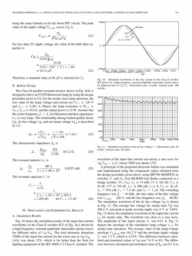
Fig. 10 shows the simulation results of the input line-currentwaveforms of the Class-E rectifier ICS of Fig. 4(c) driven bya high-frequency constant-amplitude sinusoidal current sourcefor different ratios of . The total harmonic distortion(THD) of the input line current for the worst case at
was about 12%, which is far better than the limit forlighting equipment of the IEC-6000-3-2 Class-C standard. The
Fig. 10. Simulated waveforms of the line current in the Class-E rectifierICS driven by a high-frequency constant-amplitude sinusoidal current sourcefor different ratio of V =V . Horizontal scale: 2 ms/div. Vertical scale: 100mA/div.
Fig. 11. Simulated waveform of the dc bus voltage V . Horizontal scale: 20ms/div. Vertical scale: 40 V/div.
waveform of the input line current was nearly a sine wave for, whose THD was about 3.5%.
A prototype of the proposed electronic ballast was simulatedand implemented using the component values obtained fromthe design procedure given above, using IRF740 MOSFETs asswitches and , four MUR460 fast diodes connected as abridge rectifier - , mH, nF,
nF, nF, H, , F,H, nF, and F. The switching
frequency was kHz, the rms value of the line voltagewas V, and the line frequency was Hz.The simulation waveform of the dc bus voltage is shownin Fig. 11. The average bus voltage for steady-state was208.4 V, and peak-to-peak envelop ripple was 8 V or 3.84%.Fig. 12 shows the simulation waveform of the input line current
for steady state. The waveform was close to a sine wave.The amplitude of line input current was 0.41 A. Fig. 13depicts the envelope of the simulation lamp voltage forsteady-state operation. The average value of the lamp-voltageenvelope was 161.2 V and the envelope ripple voltage
was 7.3 V, which is 4.53%. The difference between calcu-lated and simulated values of was 7.6 V or 4%. The differ-ence between calculated and simulated value of was 0.1 A or

146 IEEE TRANSACTIONS ON CIRCUITS AND SYSTEMS—I: REGULAR PAPERS, VOL. 53, NO. 1, JANUARY 2006
Fig. 12. Simulated waveform of the input line current i . Horizontal scale: 5ms/div. Vertical scale: 100 mA/div.
Fig. 13. Simulated envelope waveform of the lamp voltage � . Horizontalscale: 5 ms/div. Vertical scale: 40 V/div.
Fig. 14. Experimental waveforms of input line voltage � and current i .Horizontal scale: 5 ms/div. Vertical scale: 50 V/div. and 200 mA/div.
2.4%. The simulation showed that the lamp current crest factorwas 1.474, which is well below the maximum allowed value of1.7.
B. Experimental Results
The measured input line voltage and current waveforms areshown in Fig. 14. The THD of input line voltage and currentwere about 5.4 and 12.6%, respectively. The input power factorwas 0.992. A good sinusoidal line voltage waveform was un-available due to the isolation transformer in the laboratory facil-
Fig. 15. Experimental envelope waveform of lamp current i . Horizontalscale: 5 ms/div. Vertical scale: 100 mA/div.
Fig. 16. Measured waveforms of switch voltage of S and switch current ofS for Class-D inverter. Horizontal scale: 5 �s/div. Vertical scale: 50 V/div. and2 A/div.
Fig. 17. Measured waveforms of switch voltage of S and switch current ofS for Class-D inverter. Horizontal scale: 5 �s/div. Vertical scale: 50 V/div. and2 A/div.
ities. Fig. 15 shows the measured waveform of the lamp current.The peak value of lamp-current envelope was 283 mA and therms value of the lamp current was 208.5 mA. The lamp currentcrest factor was 1.36. The waveform of the switch voltage ofand the switch current of of the Class-D inverter are shownin Fig. 16. Fig. 17 shows the waveforms of the switch voltageand current of . It can be seen that the inverter was operatedabove resonance because the switch current was negative afterthe switch was turned on.
There was ringing in the switch current just after the switchwas turned on due to a step change in the antiparallel diodeand MOSFET current. This ringing can be attributed to theinductance of the loop required for the current probe and a

JIRASEREEAMORNKUL et al.: SINGLE-STAGE ELECTRONIC BALLAST WITH CLASS-E RECTIFIER AS POWER-FACTOR CORRECTOR 147
Fig. 18. Measured waveforms of diode current ofD and capacitor voltage ofC for the Class-E rectifier near the peak of line voltage. Horizontal scale: 10�s/div. Vertical scale: 1 A/div and 100 V/div.
Fig. 19. Measured waveforms of diode current ofD and capacitor voltage ofC for Class-E rectifier near the zero crossing of line voltage. Horizontal scale:10 �s/div. Vertical scale: 1 A/div and 100 V/div.
parasitic capacitance. Figs. 18 and 19 show the experimentalwaveforms of the diode current and the capacitor voltage
for the Class-E rectifier near the peak and the zero crossingof the line voltage, respectively. As expected, the duty cycle ofthe diode current decreased as the instantaneous line voltagedecreased. The duty cycle of the diode current at the peakof the line voltage was 0.54, whereas the calculated value ofthe duty cycle was 0.4. This difference can be attributed topower losses in the actual circuit. The measured dc bus voltagewas 183 V and its calculated value was 216 V. The totalmeasured efficiency of the ballast was 88.3%. The operatingswitching frequency was 61.3 kHz.
V. SIMPLIFIED CIRCUIT
The circuit of the proposed electronic ballast can be simpli-fied by combining two resonant circuits driving the Class-E rec-tifier and the lamp into one as shown in Fig. 20. A high-leakagecoupling transformer can be used. The advantages of the sim-plified circuit are: 1) the number of inductive components is re-duced; 2) the switch peak currents are reduced; and, thus, 3) theconduction losses in the main switches are reduced. The disad-vantage is a difficulty to design the circuit because the current inthe ICS semistage interacts with the current in the lamp resonantcircuit. When a low THD of the line current is achieved, thelamp current has the crest factor higher than the recommendedvalue of 1.7 from lamp manufacturers.
Fig. 20. Simplified ballast circuit by combining two resonant circuits drivingthe Class-E rectifier and the lamp into one.
VI. CONCLUSION
A single-stage high-power-factor electronic ballast with aClass-E rectifier as a PFC has been proposed in this paper.The Class-E rectifier is inserted between the front-end bridgerectifier and the bulk filter capacitor to increase the conductionangle of the bridge-rectifier diode current for obtaining lowline current harmonics. A high-frequency sinusoidal currentsource, which is used to drive the Class-E rectifier, is obtainedfrom the square-wave output voltage of the Class-D resonantinverter through an resonant circuit. A high-frequencytransformer is used for impedance matching. The experimentalresults for a 32-W prototype ballast are given. The switchingfrequency was 61.3 kHz. At full power, the power factor was0.992 and the total efficiency was 88.3%. The lamp-currentcrest factor was about 1.36, which is a very good result.The proposed PFC can be used in other applications. Theproposed ballast can be simplified by combining two resonantcircuits driving the Class-E rectifier and the lamp into oneresonant circuit at the expenses of the circuit performance, i.e.,line-current power factor or lamp-current crest factor. A studyof EMC performance of the proposed ballast is recommendedfor future research.
REFERENCES
[1] M. K. Kazimierczuk and W. Szaraniec, “Electronic ballast for fluores-cent lamps,” IEEE Trans. Power Electron., vol. 8, no. 4, pp. 386–395,Aug. 1993.
[2] J. Qian and F. C. Lee, “Charge pump power-factor-correction technolo-gies, part I: concept and principle,” IEEE Trans. Power Electron., vol.15, no. 1, pp. 121–129, Jan. 2000.
[3] , “Charge pump power-factor-correction technologies, part II:ballast applications,” IEEE Trans. Power Electron., vol. 15, no. 1, pp.130–139, Jan. 2000.
[4] M. A. Co, D. S. L. Simonetti, and J. L. F. Vieira, “High-power-factorelectronic ballast based on a single power processing stage,” IEEE Trans.Ind. Electron., vol. 47, no. 4, pp. 809–820, Aug. 2000.
[5] J. Calleja and J. M. Alonso et al., “Design and experimental results of aninput-current-shaper based electronic ballast,” IEEE Trans. Power Elec-tron., vol. 18, no. 2, pp. 547–557, Mar. 2003.
[6] M. K. Kazimierczuk, “Class E low d� =dt rectifier,” Proc. Inst. Elec.Eng., Pt. B, Electric Power Appl., vol. 136, pp. 257–262, Nov. 1989.
[7] , “Analysis of Class E zero-voltage-switching rectifier,” IEEETrans. Circuits Syst., vol. 37, no. 6, pp. 747–755, Jun. 1990.
[8] M. K. Kazimierczuk and W. Szaraniec, “Class D zero-voltage switchinginverter with only one shunt capacitor,” Proc. Inst. Elec. Eng., Pt. B,Electric Power Appl., vol. 139, pp. 449–459, Sep. 1992.
[9] M. K. Kazimierczuk and D. Czarkowski, Resonant Power Con-verters. New York: Wiley, 1995.

148 IEEE TRANSACTIONS ON CIRCUITS AND SYSTEMS—I: REGULAR PAPERS, VOL. 53, NO. 1, JANUARY 2006
Kamon Jirasereeamornkul was born in Phuket,Thailand, in 1975. He received the B.Eng. degreeand the M.Eng. degree in electrical engineering fromKing Mongkut’s University of Technology Thon-buri (KMUTT), Bangkok, Thailand, in 1997 and2001, respectively, where he is currently workingtoward the Ph.D. degree in electrical and computerengineering.
In 2003 and 2004, he was a Research Associatewith the Department of Electrical Engineering,Wright State University, Dayton, OH. His research
interests are high-frequency power converters and electronic ballasts.
Marian K. Kazimierczuk (M’91–SM’91–F’04)received the M.S., Ph.D., and D.Sci. degrees fromWarsaw University of Technology, Warsaw, Poland,in 1971, and 1978, and 1984, respectively, all inelectronics engineering.
He was a Teaching and Research Assistantfrom 1972 to 1978 and Assistant Professor from1978 to 1984 with the Department of Electronics,Institute of Radio Electronics, Warsaw Universityof Technology, Poland. In 1984, he was a ProjectEngineer for Design Automation, Inc., Lexington,
MA. In 1984 and 1985, he was a Visiting Professor with the Departmentof Electrical and Computer Engineering, Virginia Polytechnic Institute andState University, Blacksburg. Since 1985, he has been with the Department ofElectrical Engineering, Wright State University, Dayton, OH, where he is cur-rently a Professor. His research interests are in high-frequency high-efficiencyswitching-mode tuned power amplifiers, resonant and PWM dc/dc powerconverters, dc/ac inverters, high-frequency rectifiers, power-factor correction,modeling and control of power converters, high-frequency magnetic devices,power semiconductor devices, electronic ballasts, RF transmitters, sensors, andsuperconductivity. He is the coauthor of the books Resonant Power Converters(Wiley, 1995), Electronic Devices, A Design Approach (Prentice-Hall, 2004),and Lab Manual for Electronic Circuits (Prentice-Hall, 2004). He has publishedover 250 technical papers, 95 of which have appeared in IEEE publications. Healso holds eight patents.
Prof. Kazimierczuk was the recipient of the IEEE Harrell V. Noble Awardfor his contributions to the fields of aerospace, industrial, and power electronicsin 1991. He is also a recipient of the 1991 Presidential Award for Faculty Ex-cellence in Research, the 1993 and 2000 College of Engineering and ComputerScience Teaching Awards, the 1995 Presidential Award for Outstanding Fac-ulty Member, the 1996–2000 Brage Golding Distinguished University Professorof Research Award from Wright State University, the 1997 and 2002 CollegeProfessional Service Awards, and the 2004 Wright State University Board ofTrustees’ Award. He was an Associate Editor of the IEEE TRANSACTIONS ON
CIRCUITS AND SYSTEMS—I: REGULAR PAPERS (formerly IEEE TRANSACTIONS
ON CIRCUITS AND SYSTEMS—I: FUNDAMENTAL THEORY AND APPLICATIONS)in 1993–1995, 1997–2001, 2002–2003, and 2004–2005. He serves as an Asso-ciate Editor of the IEEE TRANSACTIONS OF INDUSTRIAL ELECTRONICS. He wasan Associate Editor of the Journal of Circuits, Systems, and Computers. He wasa member of the Superconductivity Committee of the IEEE Power ElectronicsSociety. He was and is a chair of the CAS Technical Committee of Power Sys-tems and Power Electronic Circuits in 2001–2002 and 2004–2005. He served asa Track Chair, Co-Chair, and Program Committee Member of the IEEE Inter-national Symposium on Circuits and Systems. He is a member of Tau Beta Pi.
Itsda Boonyaroonate was born in Nakornpathom,Thailand, in 1974. He received the B.Eng. degreein electronics and telecommunication engineeringfrom King Mongkut’s University of TechnologyThonburi (KMUTT), Bangkok, Thailand, in 1996,and the M.Eng. and Ph.D. degrees in electrical andelectronics engineering from the Nippon Instituteof Technology, Saitama, Japan, in 1999 and 2002,respectively.
He was with the Electronics and Telecommunica-tion Engineering Department, KMUTT, from 2002 to
2003, where he is currently an Assistant Professor with the Electrical Engi-neering Department. His research interests include high-frequency and high-efficiency switching power converters, ZVS and ZCS inverters, single-stagepower factor correctors for low-voltage/high-power density ac-dc converters,compact inverters for electroluminescent devices, and spread-spectrum tech-nique for ac drive.
Kosin Chamnongthai (S’88–M’90) was born inBangkok, Thailand, in 1960. He received the B.Eng.degree in applied electronic engineering from theUniversity of Electro-communication (UEC), Tokyo,Japan, in 1985, the M.Eng. degree in electrical engi-neering from Nippon Institute of Technology (NIT),Saitama, Japan, in 1987, and the D.Eng. degree inelectrical engineering from Keio University, Tokyo,Japan, in 1991.
He was with the Electronic and Telecommunica-tion Engineering Department, King Mongkut’s Uni-
versity of Technology Thonburi (KMUTT), Bangkok, Thailand, as a Lecturerin 1991 and an Assistant Professor in 1993, and he has been an Associate Pro-fessor there since 1996. His current research interests include image processing,computer vision, robot vision, and natural language processing.
Dr. Chanmongthai is a member of IPS, TRS, the Institute of Electrical, Infor-mation and Communication Engineers, Japan, and ECTI.