simulating the thermal response of thin … · the simulation tool is validated using known...
TRANSCRIPT
1 Copyright © 2012 by ASME
Proceedings of the 12th
International Conference on Nuclear Engineering IMECE12
November 12-15, 2012, Houston, TX, USA
IMECE2012-87674
SIMULATING THE THERMAL RESPONSE OF THIN FILMS DURING PHOTONIC CURING
Martin J. Guillot University of New Orleans
New Orleans, LA, USA
Steve. C. McCool Novacentrix, Inc. Austin, TX, USA
Kurt A. Schroder Novacentrix, Inc. Austin, TX USA
ABSTRACT A new technology utilizing short high-intensity pulsed xenon
flashlamps has been termed "photonic curing", and has become
an efficient method for thermally processing thin film metal
inks on inexpensive, low temperature substrates. For each
film/substrate combination there is an optimum set of pulse
conditions that will cure a given material stack most efficiently
without damaging the substrate. The temperature distribution in
the film stack is controlled by varying one or more of several
pulse parameters such as peak intensity, pulse length, and
frequency of pulse repetition. Given the large combination of
possible pulse parameters and candidate materials, it is critical
to be able to determine the set of pulse conditions that most
efficiently cure the various possible combinations of candidate
material stacks without damaging them. In this effort, a
modeling tool is developed to simulate photonic curing. The
model couples a transient 1-D heat conduction model to an
intuitive graphical user interface, and contains a comprehensive
materials database of temperature-dependent thermal and
material properties for a large number of candidate film
materials. The governing heat conduction equation is
discretized using the finite volume method, including an
algorithm to optimize mesh spacing and time stepping based on
spatial and temporal temperature gradients. The simulation tool
is validated using known analytical and semi-analytical
solutions based on Green's function solutions. It is then applied
to a typical film stack used in photonic curing.
INTRODUCTION
Flexible electronics has emerged in the past decade as
a rapidly growing technology that is continually finding new
applications in both the consumer and industrial marketplace.
Typical applications include RFID tags, photovoltaics, large
area displays, "electronic" paper and disposable sensors [1]. As
smaller, lightweight, mobile technology becomes more
prevalent in everyday usage, the demand for inexpensive,
rugged and flexible electronic circuits will continue to grow.
Flexible electronic circuits are manufactured from a
range of materials and processes, but one common method is to
use ink jet printers to deposit copper or silver nanoparticles
suspended in solvents and binders onto inexpensive flexible
substrates such as polyethylene terephthalate (PET) or
polyethylene naphthalate (PEN). The wet metal inks are dried
and then sintered to make them highly conductive. The ink jet
deposition allows for the creation of complex circuit patterns,
and the combination of ink jet deposition and flexible substrate
offers the possibility to develop web roll-to-roll processing,
substantially increasing throughput and lowering manufacturing
costs.
A bottleneck in the manufacturing of inexpensive
flexible electronic circuits has been the thermal processing of
the inks. This includes drying of the ink but may also include
higher temeprature processes, such as the sintering of deposited
nanoparticles on the substrate. Inexpensive substrates such as
PET have a working temperature of about 150 deg C, and begin
to warp and show damage even before reaching the melting
temperature, and so traditional sintering temperatures are
constrained by the melting temperatures of the substrate. Oven
heating has been one method used in the past, but this requires
films to be placed in stacks in ovens for extended periods.
Storing film stacks "offline" while they sinter in low
temperature ovens is incompatible with the goal of combining
ink jet printing technology and web roll-to-roll processing to
achieve high throughput and decreased manufacturing costs.
More recently, researchers have developed novel methods of
sintering silver nanoparticles in air without heating. For
example, Wakuda, et al, [2] sintered silver nanoparticle paste in
air by dipping into methanol. Perelaer and Schubert [3] give an
excellent discussion on various sintering methods for thin films
2 Copyright © 2012 by ASME
made from nanoparticle depositions. However, these sintering
processes took up to 2 hours, and so even though the need for
oven heating was eliminated, the processing time was still long
and incompatible with roll-to-roll manufacturing.
Heating with pulsed flashlamps has been termed
"photonic curing", and is a new method for thermally
processing thin film metal inks on inexpensive, low temperature
substrates. The process was developed by Novacentrix, Inc. in
Austin, TX is described by Schroder, et al. [4], [5]. It was born
out of the needs of the printed electronics industry to develop
higher volume, less expensive methods to manufacture products
that incorporate flexible electronic circuits. The process uses
high power, short duration pulses of light from specifically
designed xenon flashlamps to thermally process thin films
printed on low temperature substrates. If the pulse of light is
short enough, the thin film can be heated to a temperature far
beyond the normal maximum working temperature of the
substrate without damaging the substrate. This is exciting, since
it is now possible to thermally process films on plastic and
paper that previously required expensive, high temperature
substrates such as glass or ceramic. Typical processing times are
on the order of 1 millisecond, meaning that a photonic curing
system can cure near-instantly. This quality makes it compatible
with high-speed roll-to-roll processing. Initially, this process
was used to sinter printed metal nanoparticle inks such as silver
and copper to form electrical conductors. It is now being used
to sinter higher temperature materials such as ceramics and
semiconductors, and additional applications for photonic
processing are continually being found. Photonic systems are
now being used to dry films as well as anneal semiconductors,
and even modulate chemical reactions to make new types of
materials.
The high power, short pulses of light employed in
photonic curing heat thin films such as printed silver or copper
nanoparticles or flakes, to a high temperature for a brief
duration. The extremely short duration pulse allows this to be
done on low-temperature substrates, such as PET, even though
PET has a melting temperature of about 150 deg C. With this
technology, thin films can be processed beyond 1000 °C on the
surface of a PET substrate without damaging it, provided the
thin film is heated and then cooled down very quickly. This is
an adequate temperature to sinter many materials including
silver and copper. The pulse of light is so fast that the back side
of the substrate is not heated appreciably during the pulse. After
the pulse is over, the thermal mass of the substrate rapidly cools
the film via conduction. The pulse is usually less than a
millisecond in duration, and the time spent at elevated
temperature is only a few milliseconds. Although the substrate
at the interface with the thin film reaches a temperature far
beyond its maximum working temperature, there is not enough
time for its mechanical properties to be significantly changed.
This effect is highly desirable as the thin film has now been
processed at a temperature which would severely damage the
substrate if processed with an ordinary oven. It often allows the
replacement of high-temperature substrates with lower-
temperature (e.g. cheaper) alternatives. Since most thermal
processes are Arrhenius in nature, i.e., the curing rate is related
to the exponential of the temperature, this short process can, in
many cases, replace extended periods of processing in a 150 °C
oven. This further means that if the light is pulsed rapidly and
synchronized to a moving web, it can replace a large festooning
oven in a space of about 50 cm. In addition to curing materials
quickly, higher temperature materials such as semiconductors or
ceramics that cannot ordinarily be cured on a low-temperature
substrate can now be cured using this technology.
Another of the more remarkable aspects of this
technology is that materials can be cured with the economics
and uniformity of oven curing but also with the control of laser
processing. Photonic curing is completely maskless. Printed
thin-film traces are heated while the surrounding substrate is
not. This can happen because most inexpensive substrate
materials, such as PET, PE, PEN, PC, PI, or even paper, do not
readily absorb light. More specifically, the absorption depth for
most of the emission from our system is much larger for those
materials as compared to many of the materials suitable for
functional inks and thin films. Thus, the substrate does not get
as hot as the thin film. This effect allows one to cure a printed
thin film with pulsed radiation on a low-temperature substrate
without the need for registration. Of course, the substrate
underneath the film does get much hotter than its maximum
working temperature, but it does not become damaged.
For each film/substrate combination there is an
optimum set of pulse conditions that will cure a given material
stack most efficiently without damaging the substrate. The
temperature distribution in the film stack is controlled by
varying one or more of several pulse parameters such as peak
intensity, pulse length, and frequency of pulse repetition. The
resulting temperature distribution depends not only on the pulse
conditions, but also on the thermal properties of candidate
materials. Given the large combination of possible pulse
parameters and candidate materials, it is critical to be able to
determine the set of pulse conditions that most efficiently cure
the various possible combinations of candidate material stacks
without damaging them. This could be accomplished
experimentally for each set of candidate materials, but this
would be resource and time consuming, and would be neither
efficient nor cost effective. The ability to simulate photonic
curing with a fast, easy to use simulation tool has the potential
to greatly reduce the time and effort (and associated costs)
required by manufacturers using photonic curing in their
manufacturing processes.
SIMULATION TOOL DEVELOPMENT
The tool developed in this effort to simulate photonic
curing is called SimPulse, and couples a transient 1-D heat
conduction model to an intuitive graphical user interface. The
interface incorporates a large and extensible materials database
that contains temperature dependent thermal and material
properties for a large number of candidate film materials. The
3 Copyright © 2012 by ASME
governing heat conduction equation is discretized using the
finite volume method and the algorithm incorporates options for
mesh spacing and time stepping optimization based on spatial
and temporal temperature gradients. .
USER INTERFACE
The SimPulse interface was written to simulate the
PulseForge(R)
photonic curing system. Built into SimPulse is a
comprehensive database of material thermophysical properties
that users can access when setting thermophysical properties for
each layer The user interface consists of 3 main panels. The
SimPulse panel allows the user to open and close files, select
specific flash lamps, and visualize output from SimPulse
simulations. The Pulse Editor panel allows users to set pulse
waveform parameters including amplitude, duration, and total
number and frequency of pulses. The Film Editor panel allows
users to create layers within the film stack and set the
thermophysical properties within each layer. It also allows users
to set the convection boundary conditions at the upper and
lower surfaces. Clicking on the film stack opens the Film Layer
Parameter panel, which allows users to add materials from
SimPulse's material database, or to define custom materials. The
user interface is thoroughly described in the SimPulse User’s
Guide [6], and so the remainder of this work focuses on the heat
conduction model.
HEAT CONDUCTION MODEL
The in depth response of thin film stacks during
photonic curing is modeled with the transient 1-D conduction
equation subject to time dependent heat flux boundary
conditions and volumetric source heating. The equation is
written as
P
T Tc k S
t x xρ
∂ ∂ ∂ = +
∂ ∂ ∂ (1)
where ρ , P
c and k are the density, specific heat at constant
pressure and thermal conductivity, respectively, and S is a
volumetric source term. The total depth of the materials is L .
Depending on the material, the heat pulse is treated as
either a surface heat flux or as a volumetric source term based
on the absorptivity of the material. If the heat pulse as treated as
a surface flux, the boundary conditions at 0x = and x L= are
written, respectively as
( ) ( )( ) ( )
4
0 ,0 0 ,0 0
, ,
( )P
L L L L
q t q t h T T T
q t h T T
εσ∞ ∞
∞ ∞
′′ ′′= − − −
′′ = − (2)
Where ( )P
q t′′ is the pulse waveform, σ is the Stefan-Boltzman
constant, ε is the emmisivity, ,o
h∞ is the convective heat
transfer coefficient, 0
T is the surface temperature and ,0
T∞ is the
ambient surface temperature above the film stack. L refers to
the same quantities below the film stack. If the heat pulse is
treated as a volumetric source term, then ( )P
q t′′ is not included
in Eqn. (2) and the incident heat pulse flux is assumed to be
absorbed volumetrically through the film stack according Beer’s
law as
0/ lq q e α−′′ ′′ = (3)
where 0
q′′ is the incident heat flux, q′′ is the flux transmitted
through a planar volume of depth l , andα is the absorption
coefficient. Beer’s law is used to compute the fraction of the
surface heating pulse ( )P
q t′′ absorbed within each cell.
The initial temperature distribution ( ) ( )init,0T x T x=
is computed from the steady state solution assuming convection
boundary conditions at the top and bottom surfaces.
FINITE VOLUME DISCRETIZATION
Equation (1) is discretized using an implicit finite
volume method. The film stack, including substrate, is divided
into a number of finite volumes (cells) and Eqn. (1) is
integrated over each volume with temperatures defined at the
cell centers. The finite volume method offers flexibility in
domain discretization, as well as in imposing heat flux
boundary conditions.
The model implementation can handle film stacks
made from an arbitrary number of materials. Each material
constitutes a layer in the model, and for a given film stack the
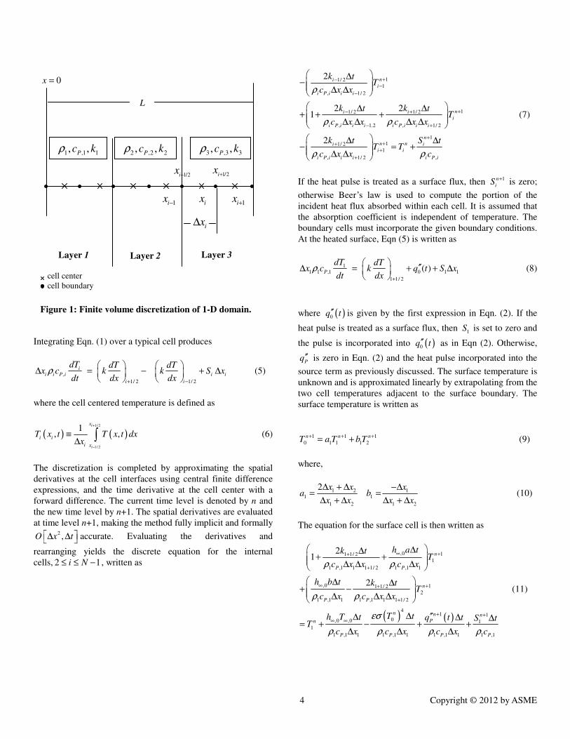
total number of layers is denoted by J. A three layer model is
showing nomenclature shown in Figure 1. Each layer is
discretized into a finite number of cells. The total number of
cells is denoted as N . The cell center is located at i
x , and the
cell boundaries are located at 1/ 2i
x ± . The grid spacing is defined
by:
( ) ( )1/ 2 1/ 2 1/ 2 1/ 2 1/ 2 1/ 2 1/ 2, i i i i i i
x x x x x x+ − ± + ± − ±∆ = − ∆ = − (4)
The properties are defined as functions of temperature within
each layer. The value of a given property is assigned to each
cell within a layer based on the cell’s current temperature.
4 Copyright © 2012 by ASME
Integrating Eqn. (1) over a typical cell produces
,
1/ 2 1/ 2
i
i i P i i i
i i
dT dT dTx c k k S x
dt dx dxρ
+ −
∆ = − + ∆
(5)
where the cell centered temperature is defined as
( ) ( )1/ 2
1/ 2
1, ,
i
i
x
i i
i x
T x t T x t dxx
+
−
≡∆ ∫ (6)
The discretization is completed by approximating the spatial
derivatives at the cell interfaces using central finite difference
expressions, and the time derivative at the cell center with a
forward difference. The current time level is denoted by n and
the new time level by n+1. The spatial derivatives are evaluated
at time level n+1, making the method fully implicit and formally 2,O x t ∆ ∆ accurate. Evaluating the derivatives and
rearranging yields the discrete equation for the internal
cells, 2 1i N≤ ≤ − , written as
11/ 2
1
, 1/ 2
11/ 2 1/ 2
, 1.2 , 1/ 2
1
11/ 2
1
, 1/ 2 ,
2
2 21
2
ni
i
i P i i i
ni i
i
i P i i i i P i i i
n
n ni i
i i
i P i i i i P i
k tT
c x x
k t k tT
c x x c x x
k t S tT T
c x x c
ρ
ρ ρ
ρ ρ
+−−
−
+− +
− +
+++
+
+
∆− ∆ ∆
∆ ∆+ + + ∆ ∆ ∆ ∆
∆ ∆− = + ∆ ∆
(7)
If the heat pulse is treated as a surface flux, then 1n
iS + is zero;
otherwise Beer’s law is used to compute the portion of the
incident heat flux absorbed within each cell. It is assumed that
the absorption coefficient is independent of temperature. The
boundary cells must incorporate the given boundary conditions.
At the heated surface, Eqn (5) is written as
1
1 1 ,1 0 1 1
1 1/ 2
( )P
dT dTx c k q t S x
dt dxρ
+
′′∆ = + + ∆
(8)
where ( )0q t′′ is given by the first expression in Eqn. (2). If the
heat pulse is treated as a surface flux, then 1
S is set to zero and
the pulse is incorporated into ( )0q t′′ as in Eqn (2). Otherwise,
Pq′′ is zero in Eqn. (2) and the heat pulse incorporated into the
source term as previously discussed. The surface temperature is
unknown and is approximated linearly by extrapolating from the
two cell temperatures adjacent to the surface boundary. The
surface temperature is written as
1 1 1
0 1 1 1 2
n n nT a T b T+ + += + (9)
where,
1 2 1
1 1
1 2 1 2
2 x x xa b
x x x x
∆ + ∆ −∆= =
∆ + ∆ ∆ + ∆ (10)
The equation for the surface cell is then written as
( ) ( )
,0 11 1/ 2
1
1 ,1 1 1 1/ 2 1 ,1 1
,0 11 1/ 2
2
1 ,1 1 1 ,1 1 1 1/ 2
41 1
0,0 ,0 1
1
1 ,1 1 1 ,1 1 1 ,1 1 1 ,1
21
2
n
P P
n
P P
n n nPn
P P P P
h a tk tT
c x x c x
h b t k tT
c x c x x
T th T t q t t S tT
c x c x c x c
ρ ρ
ρ ρ
εσ
ρ ρ ρ ρ
∞ ++
+
∞ ++
+
+ +∞ ∞
∆∆+ + ∆ ∆ ∆
∆ ∆+ − ∆ ∆ ∆
∆ ′′∆ ∆ ∆= + − + +
∆ ∆ ∆
(11)
Figure 1: Finite volume discretization of 1-D domain.
1 ,1 1, ,P
c kρ 2 ,2 2, ,P
c kρ 3 ,3 3, ,P
c kρ
ix
1/2ix
+
1/2ix
−
1ix + 1ix −
ix∆
L
Layer 1 Layer 2 Layer 3
0x =
cell center
cell boundary
5 Copyright © 2012 by ASME
where only one of the last two terms on the RHS is retained,
depending on how the heat pulse is treated. The radiation heat
flux term is linearized by evaluating it at the known time level,
n. Similarly, the bottom surface is discretized as
, 11/ 2
1
, , 1/ 2
, 11/ 2
, 1/ 2 ,
1, , 1
, ,
2
21
L N nN
N
N P N N N P N N N
L N nN
N
N P N N N N P N N
nL Ln
N
N P N N N P N
h b t k tT
c x c x x
h a tk tT
c x x c x
h T t S tT
c x c
ρ ρ
ρ ρ
ρ ρ
∞ +−−
−
∞ +−
−
+∞ ∞
∆ ∆− ∆ ∆ ∆
∆∆+ + + ∆ ∆ ∆
∆ ∆= + +
∆
(12)
Linear extrapolation is used to compute the bottom surface
temperature similarly as in done with top surface temperature,
and N
a and N
b are defined analogously to Eqn. (10). The
previous comments about the source term apply to Eqn. (12) as
well. Eqns. (7), (11) and (12) form a tridiagonal system of
equations that are solved at each time step to compute the
temporal evolution of the temperature distribution within the
film stack from a given initial distribution ( )0,T x .
MODEL VALIDATION
The implementation of the numerical model is
validated using a sequence of test cases with known analytical
or approximate analytical solutions. The cases and results are
described below.
CASE 1: This case is a slab of finite thickness, L , with
a uniform initial temperature distribution is i
T at 0t = , and the
temperature on the left boundary is suddenly raised to o
T for
0t > . The right boundary is adiabatic. Defining non-
dimensional variables ( ) ( )0/
i iT T T Tθ = − − , ( )2
/ L tτ α= ,
/x Lξ = , and ( )1/ 2n
nλ π= + , the analytical solution is
written as
( ) ( )0
, 1 2 sinn
n
n n
ex t
λ τ
θ λ ξλ
−∞
=
= − ∑ (13)
The constant temperature boundary condition is imposed
weakly by specifying a convection boundary condition with
heat transfer coefficient, 1010T
h = and setting the ambient
temperature to the desired surface temperature. SimPulse was
run for 5.46x10⁻⁶
seconds for a 10 micron layer of copper with
thermal diffusivity, 41.165x10α −= m2/s. The results were non-
dimensionalized with the above scales to compare to the
analytical solution.
SimPulse was run with a highly refined mesh (1000
cells) and small time step (2000 time steps) to ensure converged
solutions so that comparison with analytical solution could be
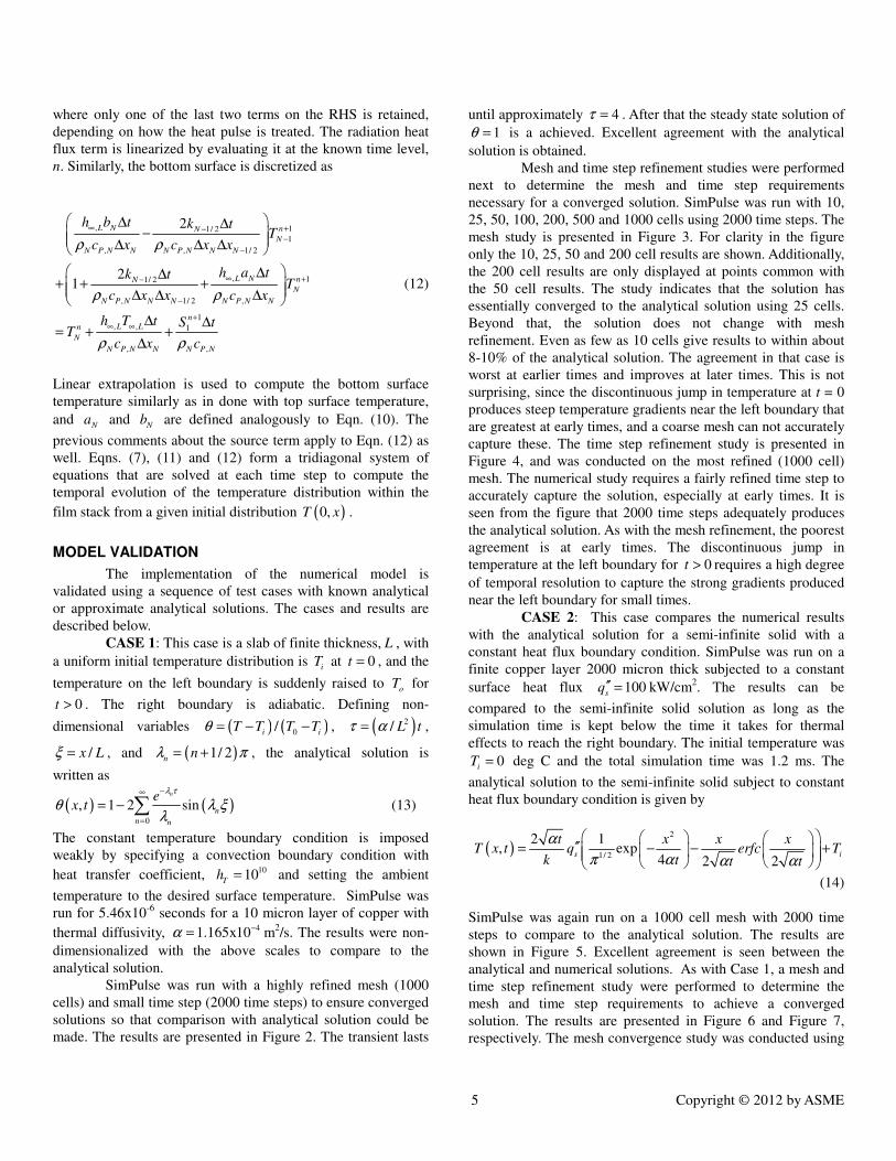
made. The results are presented in Figure 2. The transient lasts
until approximately 4τ = . After that the steady state solution of
1θ = is a achieved. Excellent agreement with the analytical
solution is obtained.
Mesh and time step refinement studies were performed
next to determine the mesh and time step requirements
necessary for a converged solution. SimPulse was run with 10,
25, 50, 100, 200, 500 and 1000 cells using 2000 time steps. The
mesh study is presented in Figure 3. For clarity in the figure
only the 10, 25, 50 and 200 cell results are shown. Additionally,
the 200 cell results are only displayed at points common with
the 50 cell results. The study indicates that the solution has
essentially converged to the analytical solution using 25 cells.
Beyond that, the solution does not change with mesh
refinement. Even as few as 10 cells give results to within about
8-10% of the analytical solution. The agreement in that case is
worst at earlier times and improves at later times. This is not
surprising, since the discontinuous jump in temperature at t = 0
produces steep temperature gradients near the left boundary that
are greatest at early times, and a coarse mesh can not accurately
capture these. The time step refinement study is presented in
Figure 4, and was conducted on the most refined (1000 cell)
mesh. The numerical study requires a fairly refined time step to
accurately capture the solution, especially at early times. It is
seen from the figure that 2000 time steps adequately produces
the analytical solution. As with the mesh refinement, the poorest
agreement is at early times. The discontinuous jump in
temperature at the left boundary for 0t > requires a high degree
of temporal resolution to capture the strong gradients produced
near the left boundary for small times.
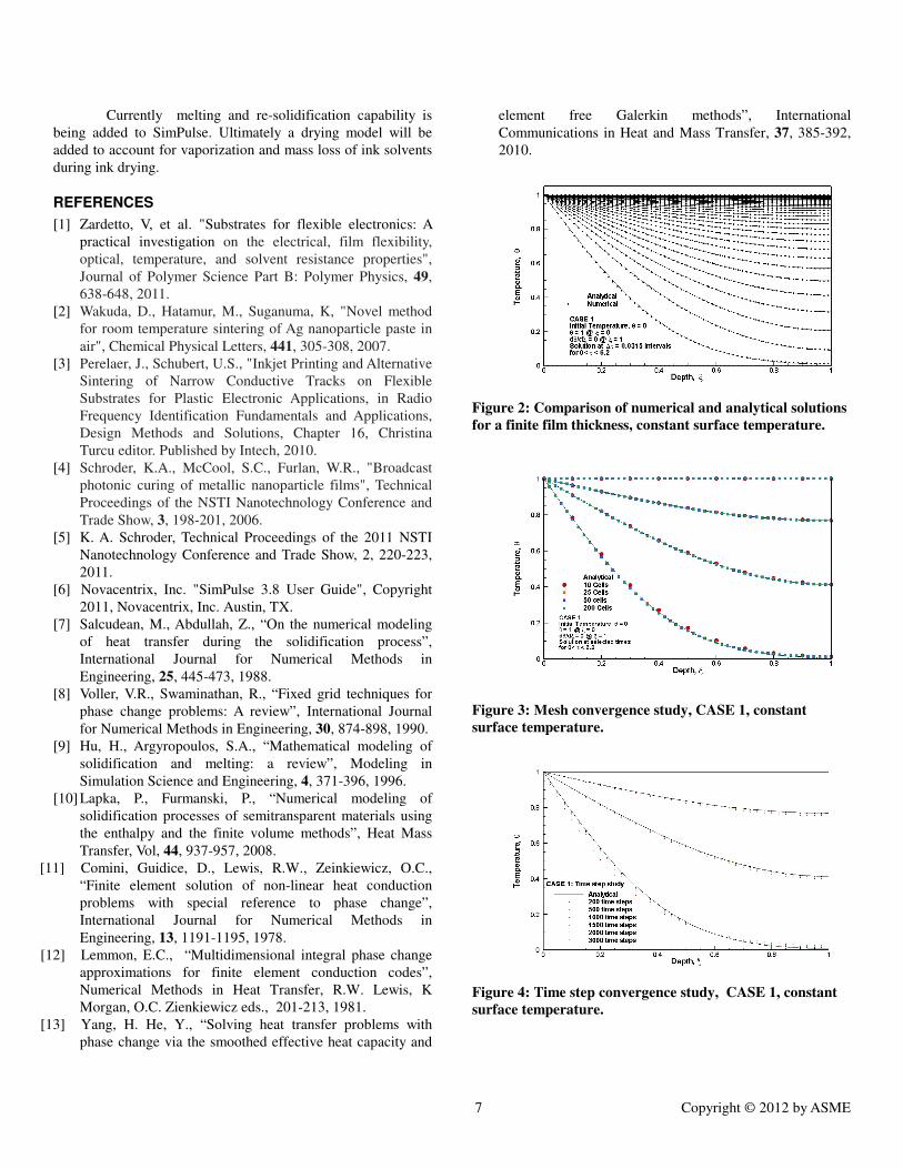
CASE 2: This case compares the numerical results
with the analytical solution for a semi-infinite solid with a
constant heat flux boundary condition. SimPulse was run on a
finite copper layer 2000 micron thick subjected to a constant
surface heat flux 100s
q′′ = kW/cm2. The results can be
compared to the semi-infinite solid solution as long as the
simulation time is kept below the time it takes for thermal
effects to reach the right boundary. The initial temperature was
0i
T = deg C and the total simulation time was 1.2 ms. The
analytical solution to the semi-infinite solid subject to constant
heat flux boundary condition is given by
( )2
1/ 2
2 1, exp
4 2 2s i
t x x xT x t q erfc T
k t t t
α
απ α α
′′= − − +
(14)
SimPulse was again run on a 1000 cell mesh with 2000 time
steps to compare to the analytical solution. The results are
shown in Figure 5. Excellent agreement is seen between the
analytical and numerical solutions. As with Case 1, a mesh and
time step refinement study were performed to determine the
mesh and time step requirements to achieve a converged
solution. The results are presented in Figure 6 and Figure 7,
respectively. The mesh convergence study was conducted using

6 Copyright © 2012 by ASME
2000 time steps. As Figure 6 shows, the numerical solution is
converged using 50 cells. Further mesh refinement does not
change the solution. The constant wall heat flux (case 2)
requires a more refined mesh compared with the constant wall
temperature (case 1). This is because the constant wall heat flux
produces a persistently strong temperature gradient near the left
boundary that requires greater mesh refinement to accurately
capture. The time step convergence study, shown in Figure 7,
was conducted on a 1000 cell mesh. The figure indicates that
the solution is converged using as few as 50 time steps. This is
many fewer time steps than required for a converged solution
for the constant wall temperature case. This is not surprising,
since the constant wall temperature case has a discontinuous
jump in temperature at t = 0, and this requires very small time
steps to adequately capture the discontinuity.
CASE 3: Case 3 is a three pulse case that is more
representative of real conditions experienced during photonic
curing. The case consists of periods of pulsed heating followed
by periods of adiabatic diffusion. Although the adiabatic periods
are not technically “cooling”, but rather a redistribution of
temperature due to diffusion, we will, however, refer to these
periods as cooling because the surface temperature cools during
those times. While there is no purely analytical solution for this
case, semi-analytical solutions for semi-infinite solids can be
found using Green’s function solutions. Linearity of the heat
conduction equation allows the solution to be found as a
superposition of two problems. During heating cycles, the
problem can be separated into problems involving a constant
heat flux boundary condition with uniform initial conditions,
whose solution is denoted by ( , )q
T x t , and an adiabatic
evolution of temperature from an initial non-uniform
temperature distribution, whose solution is denoted by ( , )c
T x t .
During cooling cycles, the problem is strictly an evolution of
temperature from an initial non-uniform temperature
distribution. During the heating cycles, the solution to the heat
flux problem, ( , )q
T x t , is purely analytical and is given by Eqn
(14), and during the cooling cycles ( , ) 0q
T x t = . The solution to
the evolution of the temperature, ( , )c
T x t , from non-uniform
initial conditions, ( ),o o
T x t , at time o
t is given by the Green’s
function solution and is written a
( )( ) ( )
2 2
0
( , )
1, exp exp
4 44
c
L
o
T x t
x x x xT x t dx
t tt α ααπ
′ ′− − − + ′ = +
∫
(15)
This equation can be integrated numerically using Gaussian
quadrature. In this effort, ( , )c
T x t is found by integrating
forward using initial conditions at the beginning of each new
heating cycle. Note that during the first heating cycle,
( , ) 0c
T x t = because the problem begins from uniform initial
conditions, and so the “semi” analytical solution is purely
analytical and given by Eqn. (14).
The pulse length for this simulation was 500
microseconds with a pulse repetition frequency of 500 Hz. The
simulation was performed on a 5000 micron copper layer with a
pulse intensity of 210s
q′′ = kW/cm2 and total simulation time of
9000 microseconds. The surface temperature history is shown
in Figure 8, and the temperature distributions throughout the
layer at the midpoints of the pulses and cooling periods are
shown in Figure 9 for both the semi-analytical and numerical
solutions. The pulse waveform is given in the inset in Figure 8.
The numerical solutions were obtained on a 1000 cell mesh
using 2000 time steps. In both figures, excellent agreement
between the numerical and semi-analytical solutions is seen. In
Figure 9, P/C 1, 2, 3 refer to pulse and cooling periods 1, 2, and
3, respectively. The times corresponding to the midpoints of the
periods can be deduced from Figure 8.
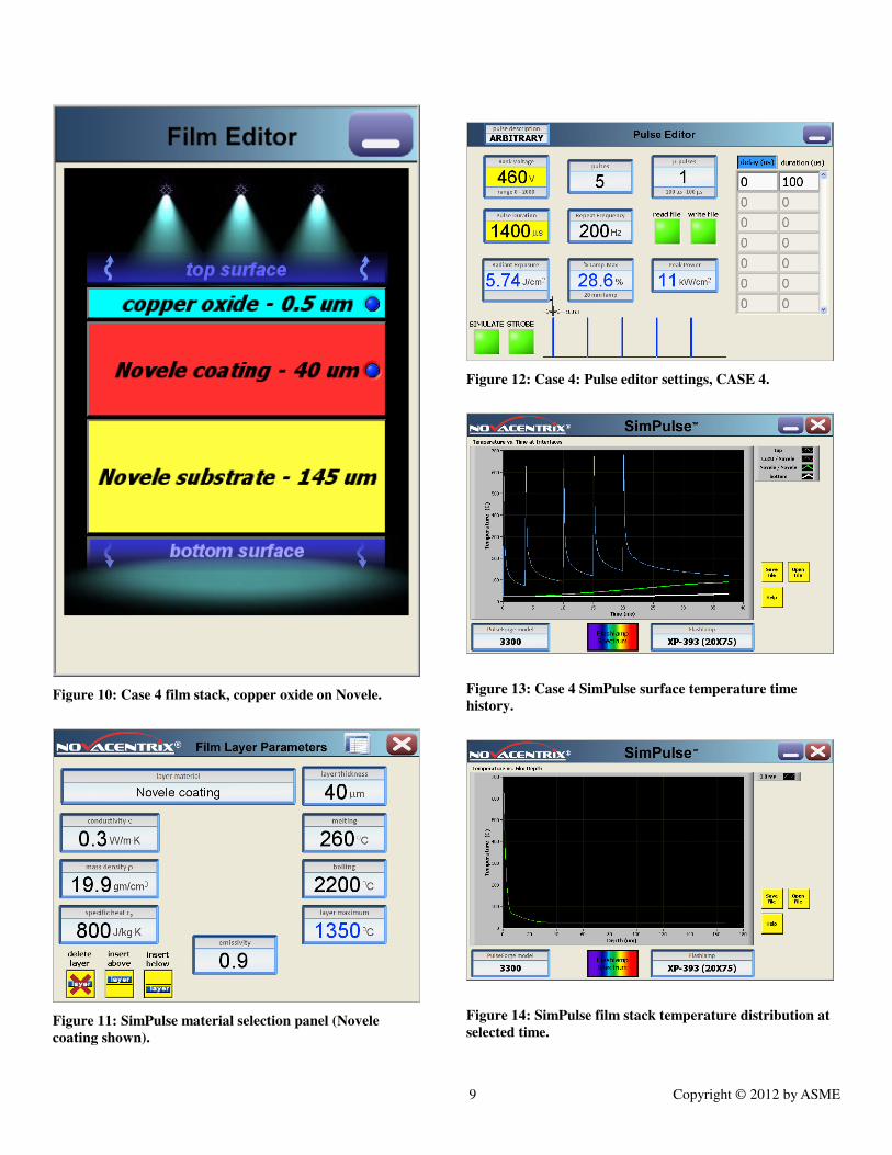
CASE 4: The final case is based on an realistic
Pulseforge application. The case is a 0.5 micron copper oxide
film on a 40 micron coating and 145 micron substrate. The
input and ouptut for this case are presented using the SimPulse
GUI to give the reader a visual sense of the SimPulse interface.
The film stack is shown in Figure 10. The Film Editor allows
the user to add/delete materials, set material properties, or use
material properties in a user database, set convective boundary
conditions at the upper and lower surface, and to specify
whether the heating is treated as a surface heat flux or
volumetric source term. Clicking on a material in the film stack
opens the Film Layer Parameters editor. The material properties
for Novele shown in Figure 11. The pulse parameters and
simulation time are set in the Pulse Editor. Since SimPulse is
designed to simulate the Pulseforge process, the user sets the
same parameters as would be set in an actual Pulseforge
application. The user sets bank voltage, pulse duration, and
number and frequency of pulses. Case 4 sets bank voltage at
460V, pulse duration of 1400 microseconds, pulse frequency
500 Hz and 5 total pulses. The quantites shown in blue are
computed by SimPulse from the user input. These settings
provide a total radiant energy exposure of 5.74 J/cm2 and an
average power of 11 kW/cm2. The surface temperature time
history is shown in the SimPules Panel (Figure 13), along with
the temperature time history at each material interface and at the
bottom of the film stack. Clicking on any selected time in the
SimPulse panel displays the temperature distribution through
the film stack at that time. The temperature distribution at 3.9
ms is shown in Figure 14.
CONCLUSIONS AND FUTURE WORK
A simulation tool to simulate the photonic curing
process has been developed and validated in this effort. The
model results agree well with known analytical and semi-
analytical solutions. Mesh and time step independence studies
indicate that the computed numerical solution converges to the
analytical solution under mesh and time step refinement.
7 Copyright © 2012 by ASME
Currently melting and re-solidification capability is
being added to SimPulse. Ultimately a drying model will be
added to account for vaporization and mass loss of ink solvents
during ink drying.
REFERENCES
[1] Zardetto, V, et al. "Substrates for flexible electronics: A
practical investigation on the electrical, film flexibility,
optical, temperature, and solvent resistance properties",
Journal of Polymer Science Part B: Polymer Physics, 49,
638-648, 2011.
[2] Wakuda, D., Hatamur, M., Suganuma, K, "Novel method
for room temperature sintering of Ag nanoparticle paste in
air", Chemical Physical Letters, 441, 305-308, 2007.
[3] Perelaer, J., Schubert, U.S., "Inkjet Printing and Alternative
Sintering of Narrow Conductive Tracks on Flexible
Substrates for Plastic Electronic Applications, in Radio
Frequency Identification Fundamentals and Applications,
Design Methods and Solutions, Chapter 16, Christina
Turcu editor. Published by Intech, 2010.
[4] Schroder, K.A., McCool, S.C., Furlan, W.R., "Broadcast
photonic curing of metallic nanoparticle films", Technical
Proceedings of the NSTI Nanotechnology Conference and
Trade Show, 3, 198-201, 2006.
[5] K. A. Schroder, Technical Proceedings of the 2011 NSTI
Nanotechnology Conference and Trade Show, 2, 220-223,
2011.
[6] Novacentrix, Inc. "SimPulse 3.8 User Guide", Copyright
2011, Novacentrix, Inc. Austin, TX.
[7] Salcudean, M., Abdullah, Z., “On the numerical modeling
of heat transfer during the solidification process”,
International Journal for Numerical Methods in
Engineering, 25, 445-473, 1988.
[8] Voller, V.R., Swaminathan, R., “Fixed grid techniques for
phase change problems: A review”, International Journal
for Numerical Methods in Engineering, 30, 874-898, 1990.
[9] Hu, H., Argyropoulos, S.A., “Mathematical modeling of
solidification and melting: a review”, Modeling in
Simulation Science and Engineering, 4, 371-396, 1996.
[10] Lapka, P., Furmanski, P., “Numerical modeling of
solidification processes of semitransparent materials using
the enthalpy and the finite volume methods”, Heat Mass
Transfer, Vol, 44, 937-957, 2008.
[11] Comini, Guidice, D., Lewis, R.W., Zeinkiewicz, O.C.,
“Finite element solution of non-linear heat conduction
problems with special reference to phase change”,
International Journal for Numerical Methods in
Engineering, 13, 1191-1195, 1978.
[12] Lemmon, E.C., “Multidimensional integral phase change
approximations for finite element conduction codes”,
Numerical Methods in Heat Transfer, R.W. Lewis, K
Morgan, O.C. Zienkiewicz eds., 201-213, 1981.
[13] Yang, H. He, Y., “Solving heat transfer problems with
phase change via the smoothed effective heat capacity and
element free Galerkin methods”, International
Communications in Heat and Mass Transfer, 37, 385-392,
2010.
Figure 2: Comparison of numerical and analytical solutions
for a finite film thickness, constant surface temperature.
Figure 3: Mesh convergence study, CASE 1, constant
surface temperature.
Figure 4: Time step convergence study, CASE 1, constant
surface temperature.
8 Copyright © 2012 by ASME
Figure 5: Numerical and semi-infinite solid analytical
solution, CASE 2, constant surface heat flux.
Figure 6: Mesh convergence study, CASE 2, constant
surface heat flux.
Figure 7: Time step convergence study, CASE 2, constant
surface heat flux.
Figure 8: Surface temperature history, CASE 3.
Figure 9: In depth temperature distribution at midpoints of
heating and cooling cycles, CASE 3.
9 Copyright © 2012 by ASME
Figure 10: Case 4 film stack, copper oxide on Novele.
Figure 11: SimPulse material selection panel (Novele
coating shown).
Figure 12: Case 4: Pulse editor settings, CASE 4.
Figure 13: Case 4 SimPulse surface temperature time
history.
Figure 14: SimPulse film stack temperature distribution at
selected time.