simple fabrication and pattern transfer of … · · 2015-04-10simple fabrication and pattern...
TRANSCRIPT
SIMPLE FABRICATION AND PATTERN TRANSFER OF ANODIZED ALUMINUM OXIDE MEMBRANES FOR NANOIMPRINTING
TEMPLATES X. Wang1, B.C. Barry1, S.W. Anderson2, and X. Zhang1*
1Boston University, USA, and 2Boston University Medical Center, USA
ABSTRACT This paper reports a simple, effective fabrication method for highly uniform, nanoporous anodized
aluminum oxide (AAO) membranes grown directly on silicon/quartz substrates. When combined with the subsequent pattern transfer techniques demonstrated herein, which may be achieved on a wafer level, nanoimprinting templates may be readily fabricated to enable scalable nanomanufacturing of polymeric nanorods for biomedical applications. KEYWORDS: Nanoimprint, Anodized aluminum oxide, Reactive ion etching, Polymeric nanorods INTRODUCTION
AAO represents a self-ordered nanoporous material, which is obtained from the electrochemical oxidation of aluminum films, and has been widely utilized for myriad applications [1] such as biological/chemical sensors, nano-electronic/optoelectronic devices, and medical scaffolds for tissue engineering, etc. In general, annealed and subsequently electrochemically polished aluminum foils (thick-Al) on the order of hundreds of microns, or electron beam or thermally evaporated aluminum thin films (thin-Al) on the order of several microns (or less), are used as starting materials. However, thick-Al films are brittle and difficult to handle after anodization, requiring additional steps to transfer the pattern onto other substrates. Thin-Al films, on the other hand, are mainly limited by their lack of uniformity compared to thick-Al, as well as the necessity to remove the barrier layer formed between the AAO and the substrate [2].
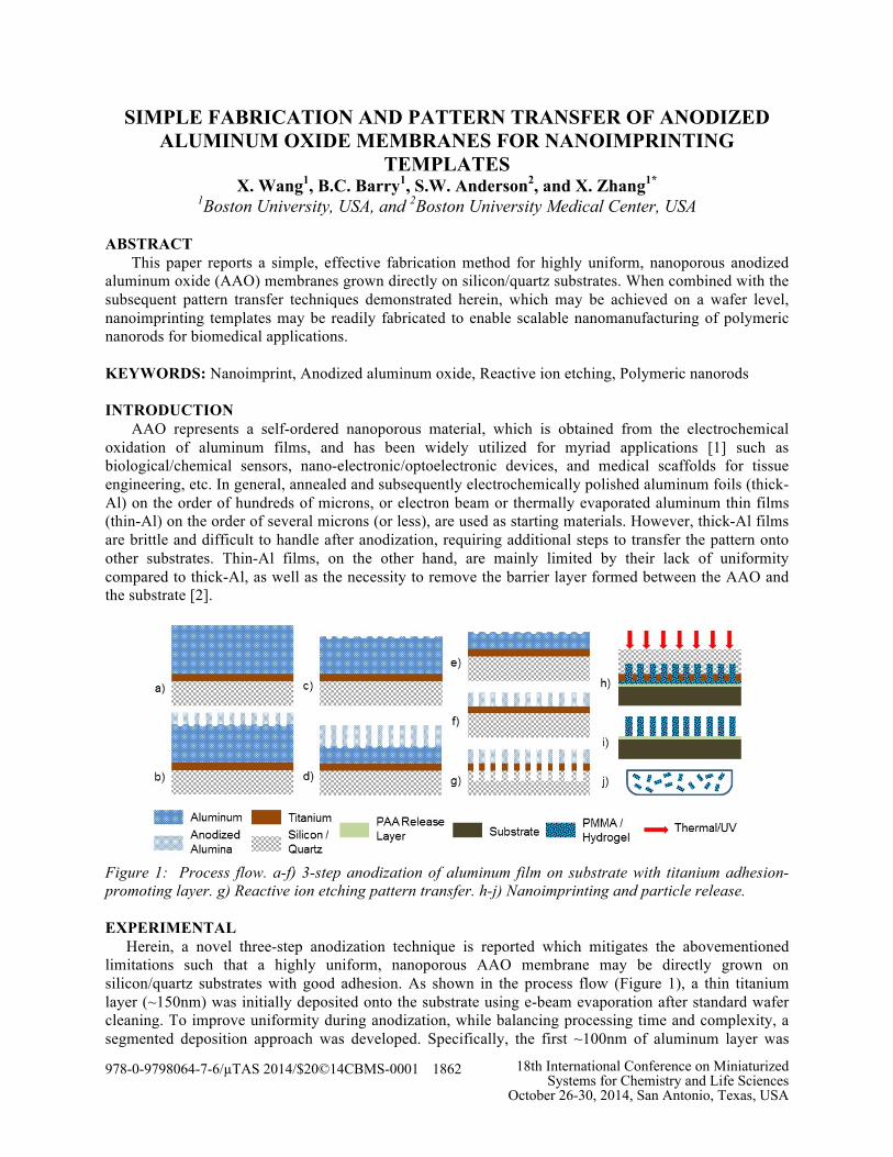
Figure 1: Process flow. a-f) 3-step anodization of aluminum film on substrate with titanium adhesion-promoting layer. g) Reactive ion etching pattern transfer. h-j) Nanoimprinting and particle release. EXPERIMENTAL
Herein, a novel three-step anodization technique is reported which mitigates the abovementioned limitations such that a highly uniform, nanoporous AAO membrane may be directly grown on silicon/quartz substrates with good adhesion. As shown in the process flow (Figure 1), a thin titanium layer (~150nm) was initially deposited onto the substrate using e-beam evaporation after standard wafer cleaning. To improve uniformity during anodization, while balancing processing time and complexity, a segmented deposition approach was developed. Specifically, the first ~100nm of aluminum layer was
978-0-9798064-7-6/µTAS 2014/$20©14CBMS-0001 1862 18th International Conference on MiniaturizedSystems for Chemistry and Life Sciences
October 26-30, 2014, San Antonio, Texas, USA

deposited at a low deposition rate (~1Å/s), followed by a ~3.8µm layer deposited at ~15Å/s, and a final ~100nm layer deposited at ~1Å/s. This approach ensures good adhesion between titanium and aluminum, as well as high initial film quality for aluminum, while achieving relatively thick aluminum layers within a reasonable processing time.
Figure 2: (A) Cross-section of aluminum layer after first anodization, showing gradually more organized pore formation downwards, with uniform divots formed at the AAO-aluminum interface. (B, C) Photos of uniform AAO membrane fabricated on both silicon (B) and quartz (C) substrate.
Anodization was then carried out in 0.3M oxalic acid solution at 1°C, with 40V applied between the
aluminum thin film anode and a stainless steel rod cathode. Under these conditions, the aluminum film was thinning at a rate of 20~30nm/min. The first anodization continued for 100 minutes (Figure 2 A) before removing the alumina layer in 5wt.% phosphoric acid (H3PO4) at 30°C for one hour. Under these same conditions, a second anodization step, followed by AAO removal, and a third, final anodization step were performed for 40 minutes, 1 hour, and 30 minutes, respectively. The final H3PO4 etching was performed for only 30 minutes to widen the pores to the desired diameter without removing the final AAO layer. Wafer-level uniform AAO membranes were successfully fabricated on both silicon and quartz substrates with excellent adhesion (Figure 2 B, C). Reactive ion etching was used to remove the barrier layer, as well as transfer the nanoporous pattern to the silicon/quartz substrate using a gas mixture of Cl2, H2 and Ar. The remaining AAO layer was subsequently removed using 1M sodium hydroxide (NaOH) solution to achieve the hybrid mold that is capable of both UV and/or thermal nanoimprinting.
Figure 3: (A, B) SEM images of AAO membrane after 3-step anodization showing homogeneous pore distribution (~90nm Ø, ~10:1 aspect ratio) and large area of uniformity from both (A) top view and (B) cross-section view with the barrier layer clearly visible. (C) Top view of titanium layer on silicon substrate after reactive ion etching followed by AAO removal in NaOH solution, demonstrating homogeneous pattern transfer results. Inset: Cross-section view of the same sample showing layered structure of the hybrid mold. *Note: Size difference of pores in substrate can be attributed to the cutting angle of the cross section.
1863
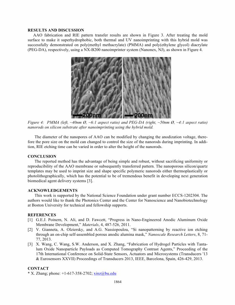
RESULTS AND DISCUSSION AAO fabrication and RIE pattern transfer results are shown in Figure 3. After treating the mold
surface to make it superhydrophobic, both thermal and UV nanoimprinting with this hybrid mold was successfully demonstrated on poly(methyl methacrylate) (PMMA) and poly(ethylene glycol) diacrylate (PEG-DA), respectively, using a NX-B200 nanoimprinter system (Nanonex, NJ), as shown in Figure 4.
Figure 4: PMMA (left, ~40nm Ø, ~6:1 aspect ratio) and PEG-DA (right, ~50nm Ø, ~4:1 aspect ratio) nanorods on silicon substrate after nanoimprinting using the hybrid mold.
The diameter of the nanopores of AAO can be modified by changing the anodization voltage, there-
fore the pore size on the mold can changed to control the size of the nanorods during imprinting. In addi-tion, RIE etching time can be varied in order to alter the height of the nanorods.
CONCLUSION
The reported method has the advantage of being simple and robust, without sacrificing uniformity or reproducibility of the AAO membrane or subsequently transferred pattern. The nanoporous silicon/quartz templates may be used to imprint size and shape specific polymeric nanorods either thermoplastically or photolithographically, which has the potential to be of tremendous benefit in developing next generation biomedical agent delivery systems [3].
ACKNOWLEDGEMENTS
This work is supported by the National Science Foundation under grant number ECCS-1202304. The authors would like to thank the Photonics Center and the Center for Nanoscience and Nanobiotechnology at Boston University for technical and fellowship supports.
REFERENCES [1] G.E.J. Poinern, N. Ali, and D. Fawcett, “Progress in Nano-Engineered Anodic Aluminum Oxide
Membrane Development,” Materials, 4, 487-526, 2011. [2] V. Gianneta, A. Olziersky, and A.G. Nassiopoulou, “Si nanopatterning by reactive ion etching
through an on-chip self-assembled porous anodic alumina mask,” Nanoscale Research Letters, 8, 71-77, 2013.
[3] X. Wang, C. Wang, S.W. Anderson, and X. Zhang, “Fabrication of Hydrogel Particles with Tanta-lum Oxide Nanoparticle Payloads as Computed Tomography Contrast Agents,” Proceeding of the 17th International Conference on Solid-State Sensors, Actuators and Microsystems (Transducers '13 & Eurosensors XXVII) Proceedings of Transducers 2013, IEEE, Barcelona, Spain, 426-429, 2013.
CONTACT * X. Zhang; phone: +1-617-358-2702; [email protected]
1864