silicon carbide bipolar junction transistors for high ... · silicon carbide bipolar junction...
TRANSCRIPT

Silicon Carbide Bipolar Junction Transistors for HighTemperature Sensing Applications
Nuo Zhang
Electrical Engineering and Computer SciencesUniversity of California at Berkeley
Technical Report No. UCB/EECS-2016-170http://www2.eecs.berkeley.edu/Pubs/TechRpts/2016/EECS-2016-170.html
December 1, 2016

Copyright © 2016, by the author(s).All rights reserved.
Permission to make digital or hard copies of all or part of this work forpersonal or classroom use is granted without fee provided that copies arenot made or distributed for profit or commercial advantage and that copiesbear this notice and the full citation on the first page. To copy otherwise, torepublish, to post on servers or to redistribute to lists, requires priorspecific permission.

Silicon Carbide Bipolar Junction Transistors for High Temperature Sensing Applications
by
Nuo Zhang
A dissertation submitted in partial satisfaction of the
requirements for the degree of
Doctor of Philosophy
in
Engineering – Electrical Engineering & Computer Sciences
in the
Graduate Division
of the
University of California, Berkeley
Committee in charge:
Professor Albert P. Pisano, Chair Professor Tsu-Jae King Liu
Professor Liwei Lin
Spring 2014

Silicon Carbide Bipolar Junction Transistors for High Temperature Sensing Applications
Copyright © 2014
by
Nuo Zhang

1
Abstract
Silicon Carbide Bipolar Junction Transistors for High Temperature Sensing Applications
by
Nuo Zhang
Doctor of Philosophy in Electrical Engineering & Computer Sciences
University of California, Berkeley
Professor Albert P. Pisano, Chair
An integrated sensing module capable of operating at high temperatures would be beneficial to a number of industrial applications, such as automotive industries, aerospace systems, industrial turbines and deep-well drilling telemetric systems. Consider industrial turbines as an example. It is important to monitor a variety of physical parameters within the hot sections of the turbines in order to increase turbine efficiency, reliability and to reduce pollution. In addition, real-time monitoring can help to detect and predict the failures of critical components in a timely fashion to reduce the maintenance costs of the systems. A high temperature integrated circuit is an important part of such systems, because it provides power management function for the energy scavenger, builds the electrical interface with MEMS-based harsh environment sensors, and amplifies the sensing signals. Therefore, it is essential to have transistors, the building blocks of integrated circuits, which can operate at high temperatures. Silicon carbide (SiC) is a promising semiconductor for high temperature applications due to its excellent electrical and physical properties. The wide bandgap energy (3.2 eV for 4H-SiC) and low intrinsic carrier concentration allow SiC semiconductor devices to function at much higher temperatures. Moreover, high breakdown electric field (3-5 MV/cm), high-saturated electron velocity (2×107 cm/s) combined with high thermal conductivity (3-5 W/cm·°C) enable SiC devices to work under extreme conditions. There are growing interests on developing high temperature integrated circuits using SiC bipolar junction transistors (BJTs) because SiC BJTs are not as strongly affected by oxide quality as SiC metal-oxide-semiconductor field effect transistors (MOSFETs). In addition, SiC BJTs are normally-off devices and have higher transconductance compared with SiC junction field effect transistors (JFETs). This dissertation presents comprehensive analytical and experimental results on 4H-SiC NPN BJTs capable of operating at high temperatures up to 400 °C. Comprehensive characterization including current gain, early voltage, output resistance, and intrinsic voltage gain was performed. At room temperature, the device has a current gain of 14.5 and an intrinsic voltage gain of 3300. At elevated temperatures, the intrinsic voltage gain increases to 5900 at 400 °C, although the current gain of the device is reduced to 6.7.
2
This suggests that 4H-SiC BJT has the potential to be used as a voltage amplifier at extremely high temperatures. High temperature effects of 4H-SiC are theoretically studied. The incomplete ionization effect and the temperature dependence of minority carrier lifetime are the two main competing mechanisms for the change of device performance with rising temperature. To further enhance the current gain, fabrication process can be improved for reduction of interface traps residing between SiC and the passivation oxide layer. This dissertation also presents the design, fabrication and characterization of a high-performance temperature sensor based on 4H-SiC pn diode. The device shows stable operation from room temperature up to 600 °C. Under forward bias condition, the temperature sensitivity of the sensor changes from 2.3 mV/°C at a forward current density of 0.44 A/cm2, to 3.5 mV/°C at a forward current of 0.44 mA/cm2. Higher sensitivity can be achieved at a lower forward current level. The experimental results indicate a good agreement with theoretical analysis. These results show that the device has the potential to be integrated with supporting circuitries to build a sensing module for high temperature applications.

i
To my parents and my husband
ii
TABLE OF CONTENTS
List of Figures ............................................................................................................. iv
List of Tables .............................................................................................................. vi
List of Abbreviations ................................................................................................. vii
Acknowledgments ...................................................................................................... xi
Chapter 1 Introduction ............................................................................................... 1
1.1 High Temperature Sensing Applications ........................................................ 1 1.2 Material Properties of Silicon Carbide ........................................................... 4
1.2.1 Crystal Structure ................................................................................... 4 1.2.2 Material Properties ............................................................................... 6
1.3 High Temperature SiC Electronics ................................................................. 6 1.4 Fundamentals of Bipolar Junction Transistors ............................................... 8 1.5 Thesis Organization ........................................................................................ 9
Chapter 2 Physical Models ........................................................................................ 11
2.1 Band Structure ................................................................................................ 11 2.1.1 Energy Bandgap and Temperature Dependence .................................. 11 2.1.2 Bandgap Narrowing .............................................................................. 12 2.1.3 Effective Masses and Effective Density of States ................................ 13
2.2 Mobility .......................................................................................................... 14 2.3 Incomplete Ionization ..................................................................................... 15 2.4 Generation-Recombination ............................................................................. 16
2.4.1 Shockley-Read-Hall Recombination .................................................... 16 2.4.2 Surface SRH Recombination ................................................................ 17 2.4.3 Auger Recombination ........................................................................... 17
Chapter 3 Microfabrication Technology of SiC Bipolar Junction Transistors .......... 19
3.1 Fabrication Process Flow of SiC Bipolar Junction Transistors ...................... 19 3.2 Fabrication Challenges ................................................................................... 22
3.2.1 Etching of Silicon Carbide ................................................................... 22 3.2.2 Metallization ......................................................................................... 25 3.2.3 Surface Passivation ............................................................................... 29
3.3 Conclusions ..................................................................................................... 30
Chapter 4 Simulation and Characterization Results of 4H-SiC Bipolar Junction Transistors ................................................................................................. 32
4.1 Device Structure ............................................................................................. 32

iii
4.2 Room Temperature Characterization of the 4H-SiC BJT ............................... 36 4.3 High Temperature Effects in 4H-SiC ............................................................. 36
4.3.1 Temperature Dependence of Carrier Concentration ............................. 36 4.3.2 Temperature Dependence of Carrier Lifetime ...................................... 40
4.4 High Temperature Characterization of 4H-SiC BJTs ..................................... 40 4.5 Effects of SiC/SiO2 Interface Traps ................................................................ 44 4.6 Conclusions ..................................................................................................... 46
Chapter 5 Fabrication and Characterization of SiC PN Diode for High Temperature Sensing Applications ........................................................... 47
5.1 Fundamentals of PN Junction Diode .............................................................. 47 5.1.1 PN Junction Electrostatics Under Equilibrium ..................................... 48 5.1.2 Current Conduction Mechanisms ......................................................... 49
5.2 Temperature Sensing Mechanism ................................................................... 50 5.3 Sensor Structure .............................................................................................. 51 5.3 Fabrication Process Flow of the Temperature Sensor .................................... 52 5.4 Characterization Results ................................................................................. 53
5.4.1 I-V Measurements at Different Temperatures ...................................... 53 5.4.2 Evaluation of the Temperature Sensor ................................................. 54
5.5 Conclusions ..................................................................................................... 56
Chapter 6 Conclusions and Future Research Directions ............................................ 57
6.1 Summary ......................................................................................................... 57 6.2 Future Research Directions ............................................................................. 59
Bibliography ................................................................................................................ 60

iv
LIST OF FIGURES
Figure 1-1. Tetrahedrally bonded Si-C cluster [1], [13]. ............................................. 4
Figure 1-2. Hexagonal close packing positions of Si-C bilayers [1], [15]. ................. 5
Figure 1-3. Stacking sequences of Si-C bilayers along c-axis for 3C-, 4H-, and 6H-SiC [15]. ............................................................................................. 5
Figure 1-4. Schematic of a NPN BJT biased at forward active region [34]. ............... 8
Figure 3-1. Cross-sectional process flow of the SiC BJT. ........................................... 20
Figure 3-2. Schematic of TCP etching system (Lam Research) [63]. ......................... 22
Figure 3-3. Scanning electron microscopy (SEM) image of the etching profile showing the trench effect. ......................................................................... 23
Figure 3-4. SEM image of the etching profile without trench effect. .......................... 24
Figure 3-5. Schematic of a transfer length method test structure and a plot of total resistance (RT) vs. contact spacing (d) [72]. .............................................. 26
Figure 3-7. TLM measurement results for Ni/Ti/Al and p-type SiC contacts. ............ 28
Figure 3-6. TLM measurement results for Ni and n-type SiC contacts under different annealing conditions. ................................................................. 28
Figure 4-1. (a) Cross-sectional schematic and (b) schematic top view of the 4H-SiC BJT. The red line in (b) indicates the position of the cross-section in (a). ......................................................................................................... 33
Figure 4-2. SEM image of the cross-section view showing the thickness of each epitaxial layer. ........................................................................................... 35
Figure 4-3. SEM image of the fabricated 4H-SiC BJT. ............................................... 35
Figure 4-4. Measured forward output characteristics (IC-VCE) with IB from 0 µA to 200 µA at room temperature (20 °C). ....................................................... 37
Figure 4-5. Measured SiC BJT base and collector current (IB and IC) and current gain (β) vs. base-emitter bias (VBE) at room temperature. ........................ 37
Figure 4-6. Simulated carrier concentration vs. temperature in the base and the emitter regions. ......................................................................................... 39
v
Figure 4-7. Simulated minority carrier lifetime vs. temperature in the base and the emitter regions. ......................................................................................... 39
Figure 4-8. High temperature probe station made by Signatone. ................................ 40
Figure 4-9. Measured forward output characteristics at different temperatures. ......... 41
Figure 4-10. Measured SiC BJT current gain vs. collector current at different temperatures (up to 400 °C). .................................................................. 42
Figure 4-11. Measured SiC BJT early voltage (VEA) and output resistance (ro) vs. temperature; the inset illustrates the base width (WB) widening effect at elevated temperatures. ........................................................................ 42
Figure 4-12. Measured SiC BJT voltage gain (Av) vs. temperature. ............................ 44
Figure 4-13. Schematic cross-sectional view of the 4H-SiC BJT presenting where the interface traps physically reside in the device. ................................. 44
Figure 4-14. TCAD simulation results of SiC BJT current gain vs. collector current with different trap concentrations. ............................................. 45
Figure 5-1. Conceptual pn junction and equilibrium energy band diagram. ............... 49
Figure 5-2. Cross-sectional schematic of the temperature sensor based on 4H-SiC pn diode. ................................................................................................... 51
Figure 5-3. SEM image of the fabricated temperature sensor based on 4H-SiC pn diode. ........................................................................................................ 52
Figure 5-4. Cross-sectional process flow of the temperature sensor. .......................... 53
Figure 5-5. I-V measurement of the 4H-SiC pn diode based temperature sensor at different temperatures (20 – 600 °C). ....................................................... 54
Figure 5-6. Measured forward voltage vs. temperature at different forward current densities. ................................................................................................... 55
Figure 5-7. Measured and modeled sensitivity vs. forward current density of the 4H-SiC pn diode temperature sensor. The extracted ideality factor and carrier lifetime are indicated on the graph. ............................................... 55

vi
LIST OF TABLES
Table 1-1. High temperature electronic applications [10]. BS stands for bulk silicon technology, SOI stands for silicon on insulator technology, WBG stands for wide bandgap semiconductor technology and NA stands for not presently available. ............................................................... 3
Table 1-2. Material properties of Si, GaAs and SiC [14]. ⊥ indicates perpendicular to c-axis, and || indicates parallel to c-axis. ................................................. 6
Table 2-1. Parameters for bandgap narrowing model of 4H-SiC in Equation (2.6)-(2.9) [38]. .................................................................................................... 13
Table 3-1. Summary of the etching recipes of crystalline 4H-SiC. ............................. 25
Table 3-2. Summary of interface state densities for SiO2/SiC interfaces. ................... 29

vii
LIST OF ABBREVIATIONS
Al Aluminum
Al2O3 Aluminum oxide Ar Argon
Av Intrinsic voltage gain α Common-base current gain
αT Base transport factor B Boron
BJT Bipolar junction transistor β Common-emitter current gain
C Carbon CF4 Tetrafluoromethane
CHF3 Trifluoromethane Cl2 Chlorine
CMOS Complementary metal-oxide-semiconductor CO Carbon monoxide CVD Chemical vapor deposition
DC Direct current DN Diffusion coefficient of electrons
DP Diffusion coefficient of holes ECR Electron cyclotron resonance
Eg Energy bandgap EA Acceptor ionization energy
ED Donor ionization energy EFn Quasi-Fermi level for n-type semiconductor
EFp Quasi-Fermi level for p-type semiconductor ε0 Vacuum permittivity
εs Relative permittivity GaAs Gallium arsenide
Gm Transconductance

viii
HBr Hydrogen Bromide HF Hydrogen Fluoride
HMDS Hexamethyldisilazane IC Integrated Circuit
ICP Inductively coupled plasma IB Base current
IC Collector current IE Emitter current
JFET Junction field effect transistor k Boltzmann constant
LN Diffusion length of electrons LP Diffusion length of holes
MESFET Metal-semiconductor field effect transistor MOSFET Metal-oxide-semiconductor field effect transistor
NB Doping concentration in the base region NC Doping concentration in the collector region
NE Doping concentration in the emitter region NA Doping concentration of p-type semiconductor
NA- Concentration of ionized acceptors
ND Doping concentration of n-type semiconductor
ND+ Concentration of ionized donors
Nc Effective density of conduction band states Nv Effective density of valance band states
Ni Nickel NO Nitric oxide
N2O Nitrous oxide n Electron concentration/Ideality factor of PN junctions
ni Intrinsic carrier concentration O2 Oxygen
PECVD Plasma enhanced chemical vapor deposition p Hole concentration

ix
ρc Specific contact resistance q Electric charge
RIE Reactive ion etching RTD Resistance temperature detector
RTA Rapid thermal annealing Rc Contact resistance
Rsh Sheet resistance ro Output resistance
γE Emitter injection efficiency factor δ Recombination factor
SEM Scanning electron microscopy Si Silicon
SiC Silicon carbide Si3N4 Silicon nitride
SiO2 Silicon dioxide SOI Silicon-on-insulator
T Temperature TCP Transformer coupled plasma
TLM Transfer length method Ti Titanium
τe Effective carrier lifetime τn Carrier lifetime of electrons
τp Carrier lifetime of holes µn Electron mobility
µp Hole mobility V Voltage
VA Early voltage VBC Base-collector voltage
VBE Base-emitter voltage VCE Collector-emitter voltage
Vbi Built-in potential

x
WB Base width Wdep Depletion width

xi
ACKNOWLEDGEMENTS
First and foremost, I would like to express my sincere gratitude to my advisor, Professor Albert P. Pisano, for his guidance and support. His contagious enthusiasm, intense dedication, and limitless patience, have set an example that I will strive to follow. I would like to thank him for all the valuable discussion, which consolidates my knowledge and also inspires me to pursue novel research directions. I am truly grateful to have had the opportunity to work and learn under his mentorship.
I would like to thank Prof. Tsu-Jae King Liu and Prof. Liwei Lin for reviewing my dissertation and giving me invaluable feedback. I would also like to thank Prof. Tsu-Jae King Liu, Prof. Liwei Lin and Prof. Ali Javey for serving on the committee of my qualifying exam. They have given me much critical and constructive feedback that helped shape this thesis.
During my tenure as a graduate student at Berkeley, I had the opportunity to work with some of the most talented people. I would like to thank all my group members and colleagues for their support. In particular I would like to thank Dr. Debbie G. Senesky, Dr. Yi Rao, Dr. Jim C. Cheng, Dr. Chih-Ming Lin, Dr. Nuo Xu, Dr. Clinton G. Warren, and Dr. Ting-Ta Yen for the valuable discussion, and their generous help and training on the fabrication and characterization tools.
I am also thankful to the Marvell Nanofabrication Laboratory staff for their help and assistance. Special thanks go to Dr. Xiaofan Meng, who helped with the deposition of different metal layers. I would also like to thank Joe Donnelly, Ryan Rivers and Jay Morford for their help and assistance on the fabrication process. At the same time, I want to thank Zeying Ren for giving me helpful suggestions and tool assistance.
Last but not least, I would like to show my deepest gratitude to my parents, for their unconditional love and support. Many thanks to my beloved husband Wenchao for being supportive all the time, and cheering me up when I am down. I am truly grateful that we worked alongside each other during this Ph.D. journey.

1
Chapter 1 Introduction
There is a rising demand for harsh-environment integrated circuits and sensors for a wide variety of applications, ranging from structure health monitoring and process control to space navigation. The ability to continually obtain information in situ in high temperature environment such as a jet engine or a deep oil well can potentially save millions of dollars and even human lives. It also opens doors to space missions to locations with extreme conditions such as Venus, where devices would be required to operate around 500 °C. Wide bandgap materials are well suited for these applications due to their superior electrical and mechanical properties compared to the silicon incumbents. 4H-SiC, a polytype of silicon carbide (SiC), for instance, has a bandgap (3.2 eV) that is almost 3 times of that of silicon (1.12 eV) [1]. The wider bandgap results in a much lower intrinsic carrier concentration compared to that of silicon [1], which makes it an ideal candidate for high temperature (> 300°C) applications. These high temperature capabilities will be the main subject of investigation in this thesis. The overarching objective of the thesis is to develop 4H-SiC technologies for both transistor and sensor devices. Specifically, we investigate and develop the design, simulation, fabrication and characterization of 4H-SiC bipolar junction transistor (BJT) that is capable of operating at elevated temperatures up to 400°C. In addition, a high-performance temperature sensor based on 4H-SiC pn diode which can stably operate in a temperature range from 20°C to 600°C is demonstrated. This type of temperature sensor can be integrated with supporting circuitries to create a sensing module that is capable of working at extremely high temperatures.
1.1 High Temperature Sensing Applications
Harsh environment conditions are typically characterized by prolonged operation at high temperatures, exposure to intense radiation and exposure to corrosion and erosion. These conditions are common to combustion engines, chemical plants, oil wells, and space missions. Electronic and sensor components that can withstand such harsh environments can be highly beneficial to these applications. The ability to place sensing units at crucial
2
hot spots can be the key enabler for a multitude of innovations that are not possible with traditional silicon-based devices. For instance, in-cylinder monitoring of a combustion engine not only provides a means to gather accurate information about the status of the engine but also enables closed-loop control that can improve combustion efficiency. In this section, we first highlight some of these applications and describe in particular their high temperature requirements. We then review current available device technologies and discuss their limitations under these requirements.
Combustion Monitoring
The continual demand for increasing fuel efficiency and reducing environmental footprints require advances in combustion controls for automotive engines and gas turbines [2]. Optimizing an engine for these objectives require precise control of temperature, pressure, air-to-fuel ratio, and timing [3]. Traditional sensing mechanisms are based on indirect measurements, which limits the scope of control methods. In-cylinder sensing, on the other hand, holds the promise that it can provide accurate and timely information about combustion events, which in turn can be utilized to develop advanced closed-loop control systems for the engines to achieve the aforementioned objectives [4]. The temperature requirements in these environments can be quite stringent. A typical engine (gasoline or diesel) has an in-cylinder temperature ranging from 200 °C to 450 °C [5]. The temperature inside a gas turbine can reach as high as 650 °C [5]. Therefore, it is crucial to develop integrated sensing modules (sensors and electronic components) that can operate reliably over an extended period of time at high temperatures, in order to unleash the full potential of these advanced control systems.
Process Control
In production environments such as an oil refinery or a chemical plant, it is important to have proper process control to maintain quality, reduce operational cost and minimize waste. Current methods for performing process control rely on periodic data interrogation that lags behind the actual process, due to inability to directly gather information in harsh environments such as a deep oil well or a reactor plant. This leads to waste of resources and inferior products. Similar to combustion monitoring, a sensing module directly placed in these environments can enable real-time monitoring of process parameters, thus allows improved process control and detects hazardous scenarios in a timely manner [6]. The peak temperature requirements can range from 300°C in an oil or gas drill to 600°C in a geothermal extraction site [10].
Space Navigation
An important sensing module that is common to these navigation systems is the inertial measurement unit (IMU) [7]. A typical IMU contains a gyroscope, an accelerometer and the necessary electronic circuits, which together are used to harvest information on a

3
craft’s velocity and orientation. However, traditional silicon devices are incapable of handling the stringent conditions often encountered by these navigation systems without extensive cooling, packaging and radiation shielding. These additional items would add volume and weight, thus placing a severe burden on the overall cost of the mission. NASA’s Venus exploration mission, for instance, would require devices to operate around 500°C.
Structural Health Monitoring
Continual monitoring in environments such as a nuclear energy production plant or a steam generator tube and pressure vessel is crucial for ensuring operation inside the safety margins. It also reduces downtime for inspection and repair that may incur expensive labor cost and disrupt the services of these plants. Hence, measuring structural changes, also known as structural health monitoring, in the critical areas, can bring significant benefits to these applications [8]. An ideal sensing module for these applications would consist of sensors such as piezoelectric or piezoresistive sensors as well as integrated electronic components with wireless capabilities. The operating conditions of these applications such as inside a nuclear energy or a high-power processing plant, however, would also require the sensing module to work at high temperatures (> 300°C) over a long period of time. This thesis explores the development of high temperature transistors and sensors based on silicon carbide that can serve as the
Table 1-1. High temperature electronic applications [10]. BS stands for bulk silicon technology, SOI stands for silicon on insulator technology, WBG stands for wide bandgap semiconductor technology and NA stands for not presently available.
High Temperature Electronic Applications
Peak Ambient (°C)
Current Technology
Future Technology
Automotive Engine Control Electronics On-cylinder & Exhaust Pipe Electric Suspension & Breaks Electric/Hybrid Vehicle PMAD
150 600 250 150
BS & SOI
NA BS BS
BS & SOI
WBG WBG WBG
Turbine Engine Sensors, Telemetry, Control Electric Actuation
300 600 150 600
BS & SOI
NA BS & SOI
BS
SOI & WBG
WBG WBG WBG
Spacecraft Power Management Venus & Mercury Exploration
150 300 550
BS & SOI
NA NA
WBG WBG WBG
Industrial High Temperature Processing
300 600
SOI NA
SOI
WBG Deep-Well Drilling Telemetry Oil and Gas Geothermal
300 600
SOI NA
SOI & WBG
WBG

4
building blocks of these integrated sensing modules. Table 1-1 categorizes these applications and lists the peak temperature requirement for each of them. Silicon (Si) based devices cannot survive at high temperatures (> 300 °C) mainly due to the high intrinsic carrier concentration which exceeds the intentional doping, and high leakage currents. Silicon-on-insulator (SOI) technology enables silicon devices to approach their theoretical limits by cutting off leakage paths. At temperatures higher than 300 °C, wide bandgap semiconductors provide solutions capable of exceeding the limits of Si. They are listed as future technologies in Table 1-1.
1.2 Material Properties of Silicon Carbide
SiC-based semiconductor electronic devices and circuits are being developed for working under extreme conditions, such as high temperature, high power, and high radiation, thanks to its superior material properties compared to Si and other semiconductors. This section briefly surveys the basic properties and advantages of SiC material.
1.2.1 Crystal Structure
SiC is a group IV-IV compound semiconductor. Each silicon (Si) atom is tetrahedrally bonded with four carbon (C) atoms, and vice versa. The approximate distance between Si-C atoms is 1.89 Å, and the distance between Si-Si or C-C atoms is 3.08 Å. The tetrahedrally bonded Si-C cluster is shown in Figure 1-1 [1], [13].
SiC exists in many different crystal structures with the same chemical composition, called polytypes [1], [13]-[15]. There are over 100 known polytypes of SiC, and the most common polytypes of SiC that have been developed for electronic applications are 3C-
Figure 1-1. Tetrahedrally bonded Si-C cluster [1], [13].
5
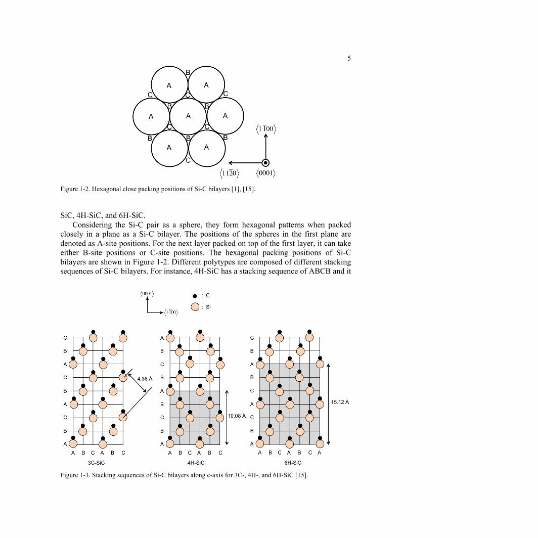
SiC, 4H-SiC, and 6H-SiC. Considering the Si-C pair as a sphere, they form hexagonal patterns when packed
closely in a plane as a Si-C bilayer. The positions of the spheres in the first plane are denoted as A-site positions. For the next layer packed on top of the first layer, it can take either B-site positions or C-site positions. The hexagonal packing positions of Si-C bilayers are shown in Figure 1-2. Different polytypes are composed of different stacking sequences of Si-C bilayers. For instance, 4H-SiC has a stacking sequence of ABCB and it
Figure 1-2. Hexagonal close packing positions of Si-C bilayers [1], [15].
Figure 1-3. Stacking sequences of Si-C bilayers along c-axis for 3C-, 4H-, and 6H-SiC [15].

6
repeats every four layers throughout the crystal. Similarly, 6H-SiC has a stacking sequence of ABCACB. Both 4H-SiC and 6H-SiC have hexagonal crystal structures. 3C-SiC, sometimes referred to as β-SiC, has a stacking sequence of ABC and it is the only form of SiC with a cubic crystal structure. The schematic structures of common polytypes of SiC are shown in Figure 1-3.
1.2.2 Material Properties
SiC is a promising semiconductor for harsh environment sensing applications due to its excellent electrical and physical properties [1]-[15]. The wide bandgap energy and low intrinsic carrier concentration allow SiC based semiconductor devices to be functional at much higher temperatures. Moreover, high breakdown field, high-saturated electron velocity, and high thermal conductivity enable SiC devices to work under extreme conditions. The basic material properties of three SiC polytypes are summarized in Table 1-2 [14]. The critical field and mobility of SiC are anisotropic, and they strongly depend on crystallographic directions of applied electric field and current flow. For comparison, the properties of Si and gallium arsenide (GaAs) are also included in Table 1-2. 4H-SiC is used in this work since it has the widest energy bandgap.
1.3 High Temperature SiC Electronics
Si semiconductor devices are usually confined to operate at temperatures < 300 °C. The intrinsic carrier concentration increases exponentially with temperature, and these free carriers could exceed the intentional doping concentration and govern the device operation in Si devices. Furthermore, the undesired junction reverse-bias leakage currents are closely related to the intrinsic carrier concentration. As the temperature increases, the
Table 1-2. Material properties of Si, GaAs and SiC [14]. ⊥ indicates perpendicular to c-axis, and || indicates parallel to c-axis.
Property Si GaAs 3C-SiC 6H-SiC 4H-SiC
Energy Bandgap [eV] 1.12 1.42 2.3 3.0 3.2 Critical Field at ND = 1017 cm-3 [MV/cm] 0.6 0.6 1.8 || 3.2
⊥ >1 || 3.0 ⊥ 2.5
Thermal Conductivity [W/cmK] 1.5 0.5 3-5 3-5 3-5
Saturated Electron Drift Velocity [107 cm/s] 1.0 1.2 2.5 2.0 2.0
Electron Mobility at ND = 1016 cm-3 [cm2/Vs] 1200 6500 750 || 60
⊥ 400 || 800 ⊥ 800
Hole Mobility at NA = 1016 cm-3 [cm2/Vs] 420 320 40 90 115
Relative Dielectric Constant 11.9 13.1 9.7 9.7 9.7

7
undesired leakage current will grow unacceptably large. SiC semiconductor devices can function at much higher temperatures than Si mainly due to the wide bandgap energy and low intrinsic carrier concentration of SiC. High temperature operation of SiC-based devices and ICs has been reported for several technologies.
The gate-insulator reliability is a critical issue for high temperature operation of SiC metal-oxide-semiconductor field effect transistors (MOSFETs), which limits the highest operating temperatures under 350 °C for SiC MOSFETs. The first high temperature depletion-mode n-channel MOSFET was fabricated and characterized by Palmour et al. from North Carolina State University in 1987. Later, Brown et al. [16][17] from General Electric (GE) reported the development of the first SiC analog IC, a monolithic MOSFET operational amplifier, based on a 6H-SiC depletion-mode n-channel MOSFET technology. In that research, stable device operation was demonstrated up to 300 °C. However, circuit drift instabilities occurred at 350 °C. Complimentary metal-oxide-semiconductor (CMOS) technologies for SiC based devices have also been investigated. Recently, Clark et al. from Raytheon UK demonstrated SiC CMOS technologies that operate at elevated temperatures up to 350 °C with low gate leakage [18].
6H-SiC junction field effect transistors (JFETs) have been also investigated notably by NASA Glenn Research and Case Western Reserve University [19]-[21]. Prolonged stable operation of 6H-SiC JFETs for thousands of hours at 500 °C has been demonstrated. The devices have also been tested at low temperatures down to -125 °C. SiC JFET differential amplifier circuits capable of operating at up to 600 °C were demonstrated by Case Western Reserve University [22]. Subsequently, basic logic gates based on 6H-SiC JFETs were reported to work at temperatures up to 550 °C [23].
6H-SiC metal-semiconductor field effect transistors (MESFETs) have also been demonstrated for high temperature operation up to 500 °C [24]. However, they suffer from significant leakage currents at the Schottky gate electrodes at higher temperatures, which limits the duration of high temperature operation.
The research on 4H-SiC bipolar junction transistors (BJTs) originally focused on high power applications. The first high voltage NPN BJT in 4H-SiC was demonstrated by Ryu et al. from Cree, Inc. in 2001 [25]. Subsequently, many efforts have been made to develop SiC power BJTs from Purdue University, Rutgers University, and Royal Institute of Technology [26]-[30]. Recently, there are growing interests on developing high temperature integrated circuits using 4H-SiC BJTs. SiC BJTs are not as strongly affected by oxide quality as SiC MOSFETs. In addition, SiC BJTs are normally-off devices and have higher transconductance compared with SiC JFETs. 4H-SiC is used due to the fact that it has the widest energy bandgap compared with other SiC polytypes, which is preferred for high temperature applications. BJTs on semi-insulating 4H-SiC was demonstrated to operate up to 355 °C by Singh et al. in 2011 [31], [32]. In this dissertation, 4H-SiC NPN BJTs for low voltage applications are presented. The devices are capable of stable operation up to 400 °C [33].
8
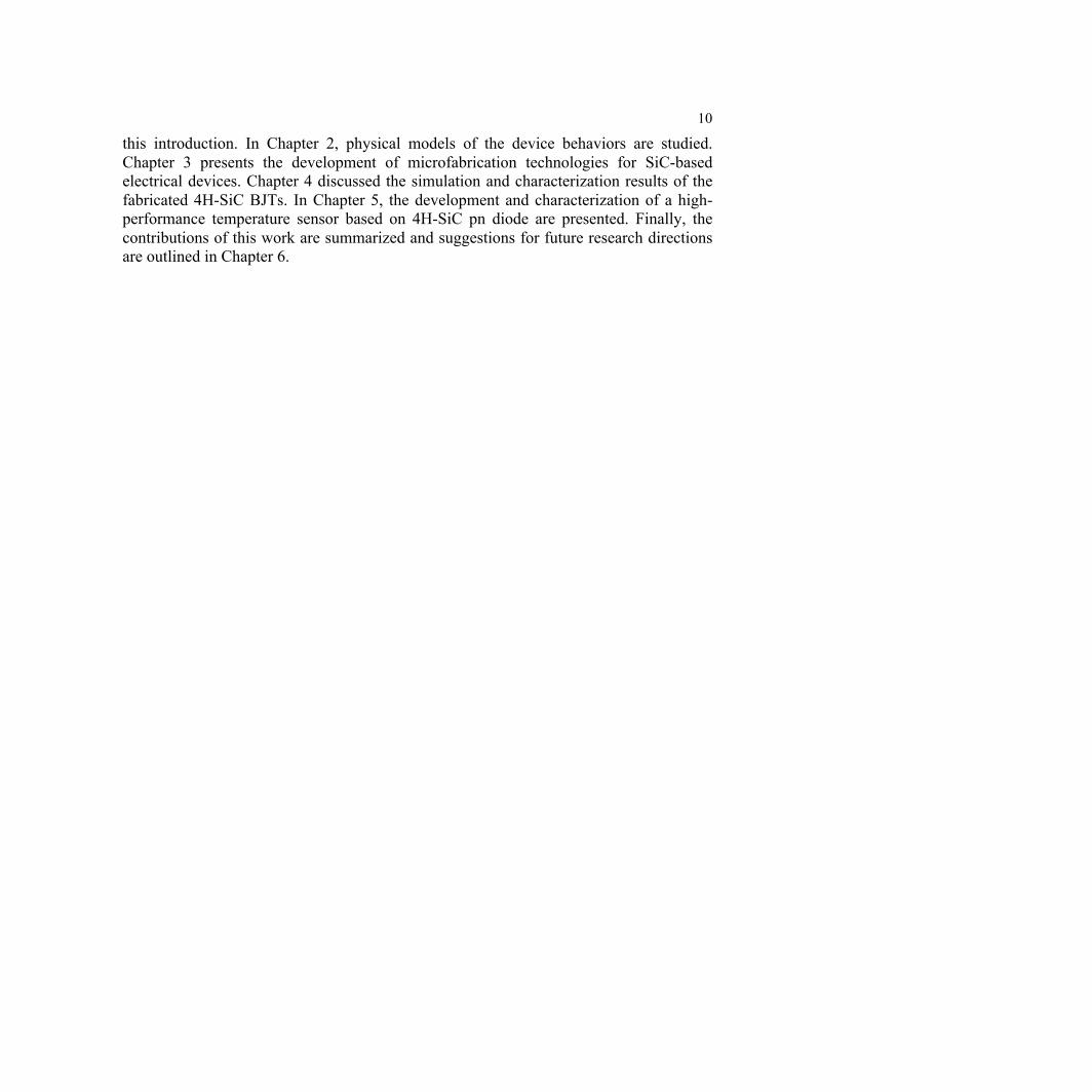
1.4 Fundamentals of Bipolar Junction Transistors
A bipolar junction transistor is a three-terminal semiconductor device [34]. The middle region is referred to as the base and it is very narrow compared with the minority carrier diffusion length in this region. The other two regions are known as the emitter and the collector. Due to the fact that electron mobility is usually higher than hole mobility, NPN BJTs are more widely used than PNP BJTs. The schematic of a NPN BJT biased in the forward active mode with carrier flux components is shown in Figure 1-4 [34]. The two junctions are referred to as the emitter-base (E-B) junction and the collector-base (C-B) junction respectively.
As pictured in Figure 1-4, the E-B junction is forward biased and the C-B junction is reverse biased in the forward active mode. The E-B junction is an n+-p one-sided junction. Therefore, more electrons are injected from the emitter to the base than holes injected from the base to the emitter. Since the quasineutral base width is much smaller than the minority carrier diffusion length, the vast majority of injected electrons that diffuses through the base can reach the depletion region of the reverse biased C-B junction. The electrons are then swept to the collector by the accelerating electrical field. The electrons injected from the emitter to the base constitute the current InE, and the holes injected from the base to the emitter give rise to the current IpE. For the one-sided n+-p junction, IpE << InE. Some electrons are lost through recombination with holes in the base (IRB). The current InC is associated with the injected electrons successfully cross the base and reach the collector. IC0 is the current of the minority carrier holes in the collector that are swept into the base in the reversed biased C-B junction. Since IC0 is a reverse biased current, IC0 << InC. The recombination-generation current associated with the depletion region of the
Figure 1-4. Schematic of a NPN BJT biased at forward active region [34].
IB
IE IC
N+ N P
InE InC
IpE IC0
IRB
Emitter Base Collector
IR

9
E-B junction is identified as IR. The total currents of the emitter, base and collector regions are given by
IE = InE + I pE + IR, (1.1) IB = I pE + IRB + IR ! IC0, (1.2) IC = InE ! IRB + IC0. (1.3)
The three currents can be related by
IE = IB + IC. (1.4)
In the common-base mode, the emitter current (IE) is the input variable while the
collector current (IC) is the output variable. α is the common base current gain, which is defined as the ration of IC/IE. It can be calculated as
! = "E!T# =InE
InE + I pE
!
"##
$
%&&InCInE
!
"#
$
%&
InE + I pEInE + IR + I pE
!
"##
$
%&&. (1.5)
In Equation (1.5), γE is the emitter injection efficiency factor, αT is the base transport factor, and δ is the recombination factor [35]. The emitter injection efficiency factor is a measure of the ability of the emitter to inject electrons into the base. The base transport factor illustrates the capability of the injected electrons to diffuse through the base without recombination. The recombination factor takes into account the recombination-generation current in the forward biased B-E junction.
In the common-emitter mode, the base current (IB) is the input variable and the collector current (IC) is the output variable. The common-emitter current gain β is defined as the ratio of IC/IB, which can be calculated as
! ="1!"
. (1.6)
The common-emitter mode is the most widely used circuit configuration. Therefore, current gain is often referred to as the common-emitter current gain β.
1.5 Thesis Organization
This work focuses on the development and characterization of 4H-SiC NPN BJTs for high temperature sensing applications. This dissertation consists of six chapters including
10
this introduction. In Chapter 2, physical models of the device behaviors are studied. Chapter 3 presents the development of microfabrication technologies for SiC-based electrical devices. Chapter 4 discussed the simulation and characterization results of the fabricated 4H-SiC BJTs. In Chapter 5, the development and characterization of a high-performance temperature sensor based on 4H-SiC pn diode are presented. Finally, the contributions of this work are summarized and suggestions for future research directions are outlined in Chapter 6.
11
Chapter 2 Physical Models
Numerical device simulators are powerful tools to investigate electrical behaviors of semiconductor devices. They can provide information of internal physical parameters that are difficult or impossible to measure. Therefore, numerical device simulators are widely used to predict and explain device performance. A real semiconductor device is represented in the simulator as a non-uniform two-dimensional (2D) or three-dimensional (3D) grid of nodes. Physical properties of the real device are discretized onto the grid. By iteratively solving a set of coupled nonlinear partial differential equations, the transport of carriers through the structure under external fields can be described. The governing equations are Poisson equation, carrier continuity equations and drift-diffusion equations. In order to obtain accurate simulation results, it is essential to utilize appropriate physical models with proper material properties. In this chapter, important physical models applied in the device simulation are introduced and discussed. Temperature dependences of the models are investigated.
2.1 Band Structure
Energy band structure is the most fundamental property of a semiconductor. Realistic band structures are complicated. For device simulation, the band structure is described by energy bandgap, effective masses and effective density of states.
2.1.1 Energy Bandgap and Temperature Dependence
Energy bandgap is the difference between the lowest energy in the conduction band and the highest energy in the valance band. As we have discussed in Chapter 1, SiC has a wider bandgap compared with Si. The bandgap of 4H-SiC is 3.23 eV at 300 K. It is not a constant value when temperature varies, and the temperature dependence of the 4H-SiC bandgap can be modeled by Equation (2.1) from [36]:

12
Eg(T ) = Eg(0)! 6.5"10!4 "T 2
T +1300 eV, (2.1)
where Eg(0) is the bandgap at 0 K, and T is the temperature in Kelvin.
2.1.2 Bandgap Narrowing
It has been reported that the bandgap of a semiconductor material shrinks when the impurity concentration is particularly high. This effect is called the bandgap narrowing effect. In a device containing adjacent regions with different doping concentrations, the displacements of band edges induced by the doping concentrations may heavily influence the device behavior. This is because the shifts of the band edges change the potential barriers in the device, which alters the carrier transport behavior across the junctions. In BJTs, the emitters are heavily doped, and therefore the bandgap narrowing effect in the emitters have to be considered in the device simulation.
Considering the bandgap narrowing effect, the effective bandgap Eg,eff can be written as
Eg,eff = Eg0 !"Ebng, (2.2)
where Eg0 is the bandgap at a low doping concentration, and ΔEbng is the shift of the bandgap due to the bandgap narrowing effect.
The intrinsic carrier concentration ni for a lightly doped semiconductor is given by Equation (2.3)
ni2 = NcNv exp
!Eg0
kT"
#$
%
&', (2.3)
where Nc and Nv are the effective density of conduction and valence band states, k is Boltzmann constant, and T is the temperature in Kelvin [37]. For BJTs, the emitter is heavily doped. The effect of bandgap narrowing on the intrinsic carrier concentration in the emitter region is given by
ni,eff2 = ni
2 exp!Ebng
kT"
#$
%
&', (2.4)
which changes exponentially with ΔEbng. For a NPN BJT, the minority carrier concentration pE0 in the emitter region can be written as
pE0 =ni,eff2
NE
=ni2
NE
exp!Ebng
kT"
#$
%
&', (2.5)

13
where NE is the doping concentration in the emitter region. Equation (2.5) shows that the bandgap narrowing effect increases the minority carrier concentration in the emitter region, which leads to a reduction of the emitter injection efficiency.
The doping-induced bandgap displacements and the bandgap narrowing effect in 4H-SiC have been modeled by Lindefelt [38]. The model is based on the theory of Jain and Roulston and is made applicable to 4H-SiC by considering the three electron effective mass components associated with hexagonal lattices. The band edge displacements for n-type and p-type semiconductors can be expressed as
!Enc = AncND
+
1018"
#$
%
&'
1/3
+BncND
+
1018"
#$
%
&'
1/2
, (2.6)
!Env = AnvND
+
1018"
#$
%
&'
1/4
+BnvND
+
1018"
#$
%
&'
1/2
, (2.7)
!Epc = ApcNA
"
1018#
$%
&
'(
1/4
+BpcNA
"
1018#
$%
&
'(
1/2
, (2.8)
!Epv = ApvNA
"
1018#
$%
&
'(
1/3
+BpvNA
"
1018#
$%
&
'(
1/2
. (2.9)
The coefficients Anc, Bnc, Anv, Bnv, Apc, Bpc, Apv, and Bpv are listed in Table 2-1, with the band edge displacements given in eV.
2.1.3 Effective Masses and Effective Density of States
For 4H-SiC, the effective density of states in the conduction band Nc can be calculated from
Table 2-1. Parameters for bandgap narrowing model of 4H-SiC in Equation (2.6)-(2.9) [38].
Anc Bnc Anv Bnv
n-type -1.50×10⁻² -2.93×10⁻³ 1.90×10⁻² 8.74×10⁻³
Apc Bpc Apv Bpv
p-type -1.57×10⁻² -6.64×10⁻⁴ 1.30×10⁻² 1.14×10⁻³
14
Nc = 4.82!1015 !M !mc
m0
"
#$
%
&'
3/2
!T 3/2 = 3.25!1015 !T 3/2 cm(3, (2.10)
where M = 3 is the number of equivalent valleys in the conduction band, and mc = 0.37m0 is the effective mass of the density of states in one valley of conduction band [36]. The effective density of states in the valance band is given by
Nv = 4.85!1015 !T 3/2 cm"3. (2.11)
2.2 Mobility
The carrier mobilities are basic inputs for expressing currents in semiconductor devices. They are dependent on doping concentration and temperature. Using the empirical relation suggested by Caughey and Thomas [39], the electron mobility µn and hole mobility µp at low electric field can be modeled as
µn,p = µn,pmin +
µn,pdelta
1+ NA + ND
Nn,pµ
!
"##
$
%&&
!n,p
T300!
"#
$
%&"n,p
, (2.12)
where NA and ND are local impurity concentrations, and the parameters are listed as below:
µnmin = 0 cm2 /V !S, µp
min =15.9 cm2 /V !S,
µndelta = 947 cm2 /V !S, µp
delta =108.1 cm2 /V !S,
Nnµ =1.94"1017 cm#3, N p
µ =1.76"1019 cm#3,!n = 0.61, ! p = 0.34,"n = #2.15, " p = #2.15.
The parameters for the doping and temperature dependences of 4H-SiC mobilities are from the work of Schaffer et al. [40].

15
2.3 Incomplete Ionization
In Si, most impurity levels are shallow enough so that the dopants can be considered fully ionized at room temperature. However, this is not the case in SiC because the donor level (ED) for nitrogen (N) and acceptor level (EA) for aluminum (Al) in SiC are relatively deep compared to the thermal energy kT. Therefore, the incomplete ionization of the impurities in SiC has to be considered even at high temperatures.
The concentration of the ionized impurity atoms is given by
ND+ =
ND
1+ gD expEFn !ED
kT"
#$
%
&', (2.14)
NA! =
NA
1+ gA expEA !EFp
kT"
#$
%
&'
, (2.15)
where ND
+ and NA- are the ionized donor and acceptor concentrations, ND and NA are the
(active) donor and acceptor concentrations, gD = 2 and gA = 4 are the degeneracy factors for the donor and acceptor levels, ED and EA are the donor and acceptor ionization energies, and EFn and EFp are the quasi-Fermi levels [41].
Impurity atoms in SiC can substitute on either the silicon or carbon sublattice. Nitrogen atoms substitute on the carbon sites, while aluminum atoms occupy the silicon sites [42]. Due to the long unit cells, inequivalent lattice sites exist in many SiC polytypes, such as 4H-, 6H- and 15R-SiC. These inequivalent lattice sites are divided into two kinds: one is hexagonal-like atomic configuration (h) and the other one is cubic-like atomic configuration (k).
For nitrogen doped n-type 4H-SiC, two inequivalent lattice sites of nitrogen (h, k) have been identified by Hall-effect and IR absorption measurements with ground state 1s(A1) binding energies of ED(h) = 52.1 meV and ED(k) = 91.8 meV [43]. The number of k-type donor sites is the same as h-type donor sites. It is worth noting that a simplification of a single donor level, ED = 65 meV below the conduction band edge, is assumed in Equation (2.14), which can be obtained by [44]
ND_ 4H!SiC+ =
0.5ND
1+ gD exp EFn !ED (h)kT
"
#$
%
&'+
0.5ND
1+ gD exp EFn !ED (k)kT
"
#$
%
&'
= ND
1+ gD exp EFn !ED
kT"
#$
%
&'.
(2.16)

16
For aluminum-doped p-type 4H-SiC, two inequivalent lattice sites should generate two energy levels in theory. However, the difference between the two acceptor levels are too small to be readily detected. Therefore, only one acceptor energy level EA = 191 meV is assumed in the calculation [45].
2.4 Generation-Recombination
Generation-recombination processes are processes that create and eliminate mobile carriers (electrons and holes). They are very important to the operation of many semiconductor devices, especially for bipolar devices. There are several mechanisms that are crucial in SiC BJTs.
2.4.1 Shockley-Read-Hall Recombination
In the indirect-bandgap semiconductors, such as Si and SiC, indirect recombination process through localized states or recombination centers is dominant. This recombination process was originally modeled by Shockley and Read [47] and later by Hall [48], and the process is commonly called Shockley-Read-Hall (SRH) recombination. The rate of SRH recombination is given by
RSRH =np! ni,eff
2
! p n+ n1( )+! n p+ p1( ), (2.17)
with n1 and p1 defined by
n1 = ni,eff expEtrap
kT!
"#
$
%&, (2.18)
p1 = ni,eff exp!Etrap
kT"
#$
%
&', (2.19)
where n and p are the electron and hole concentrations, ni,eff is the effective intrinsic carrier concentration, τn and τp are the lifetimes of electrons and holes, and Etrap is the energy difference between the defect level and the intrinsic level.
The lifetimes τn and τp depend on doping level and temperature. The doping dependence of the carrier lifetimes is described by the Scharfetter relation, and the temperature dependence is modeled by the power law.

17
! n,p =! n,pmax
1+ NA + ND
Nn,pref
!
"##
$
%&&
"n,p
T300!
"#
$
%&#n,p
, (2.20)
where τmax
n,p is the carrier lifetime in the material without impurities at 300 K, and the other parameters are listed as follows,
Nnref = 3!1017 cm"3, N p
ref = 3!1017 cm"3,!n = 0.3, ! p = 0.3,"n =1.72, " p =1.72.
The parameters for the doping dependences of 4H-SiC career lifetimes are reported in [41] and [49], and the parameters for temperature dependence are taken from [41] and [50]. Since very limited studies on the doping dependence of carrier lifetimes in 4H-SiC have been reported, it is assumed that the parameters Nref and γn,p from Si can be applied to 4H-SiC.
2.4.2 Surface SRH Recombination
At surfaces or interfaces, an additional equation is used to describe the surface SRH recombination rate, which is structurally equivalent to expression of the bulk SRH recombination rate:
RSRHsurface =
np! ni,eff2
n+ n1( ) / sp + p+ p1( ) / sn, (2.21)
where sn and sp are the surface recombination velocities for electrons and holes, n1 and p1 are defined in Equation (2.18) and Equation (2.19).
Surface recombination rate has strong impact on the current gain of SiC BJTs. It depends on the quality of the interface between silicon dioxide (SiO2) and SiC. Some methods have been reported to reduce the interface state density at the SiO2/SiC interface, which will be discussed in detail in Chapter 3.
2.4.3 Auger Recombination
In the Auger recombination process, the transition of an electron from the conduction band to the valance band is by transferring the energy to another free electron or hole by collision. Therefore, Auger recombination is a process in which three particles are involved: the recombining electron and hole, and the carrier by which the energy is absorbed. The highly energetic carrier, which gained the energy during the collision, then loses the energy in small steps through heat-producing collisions with the semiconductor

18
lattice. Auger recombination is typically important when the carrier densities are very high. Therefore, it is only likely to occur in highly doped semiconductor material or under high injection condition. The rate of Auger recombination can be modeled by [46]
RAuger = Cnn+Cpp( ) np! ni,eff2( ), (2.22)
where Cn = 5×10-31 cm-6s-1 and Cp = 2×10-31 cm-6s-1 [36].

19
Chapter 3 Microfabrication Technology of SiC Bipolar Junction Transistors
SiC single crystal material growth was first developed by Acheson process as byproducts for manufacturing industrial abrasives [51]. In 1955, Lely presented a sublimation method for SiC single crystal growth with higher quality [52]. However, Acheson process and Lely process can only produce small (~ 1 cm2) and irregular shaped SiC crystal pieces. In the late 1970s, Tairov and Tzvetkov developed a modified seeded sublimation process for growth of single crystal 6H-SiC [53], [54]. This method is also known as modified Lely method. It was a big breakthrough in the SiC industry because it made mass-production of single crystalline SiC wafers possible. After years of development of the SiC crystal growth technology, Cree, Inc. became the first company to sell 2.5 cm diameter 6H-SiC wafers in 1989, and majority of the development of SiC semiconductor electronics took place afterwards. One of the main advantages of SiC fabrication technology is that many Si process techniques can be applied to SiC process. This chapter presents an overview of the microfabrication process technology of SiC BJT devices. A baseline six-mask fabrication process is described to manufacture the proposed devices. Some issues with SiC dry etching, metallization and surface passivation are addressed. It is worth noting that some fabrication limitations described here are due to the technological limits of the semiconductor fabrication tools used in the microfabrication process. Advanced tools would allow better fabrication process in the future.
3.1 Fabrication Process Flow of SiC Bipolar Junction Transistors
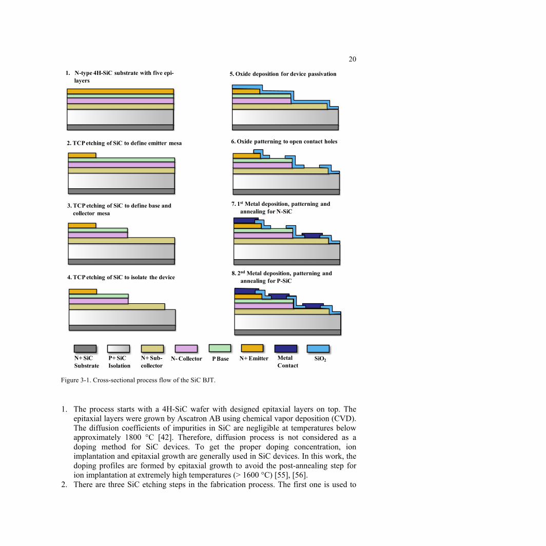
The devices were fabricated on 4° off-axis Si-face n-type 4H-SiC wafer purchased from SiCrystal AG. The fabrication process for manufacturing the SiC BJTs is based on surface micromachining techniques, and a baseline six-mask fabrication process is described as follows. The cross-sectional process flow is shown in Figure 3-1.
20
1. The process starts with a 4H-SiC wafer with designed epitaxial layers on top. The epitaxial layers were grown by Ascatron AB using chemical vapor deposition (CVD). The diffusion coefficients of impurities in SiC are negligible at temperatures below approximately 1800 °C [42]. Therefore, diffusion process is not considered as a doping method for SiC devices. To get the proper doping concentration, ion implantation and epitaxial growth are generally used in SiC devices. In this work, the doping profiles are formed by epitaxial growth to avoid the post-annealing step for ion implantation at extremely high temperatures (> 1600 °C) [55], [56].
2. There are three SiC etching steps in the fabrication process. The first one is used to
Figure 3-1. Cross-sectional process flow of the SiC BJT.
1. N-type 4H-SiC substrate with five epi-layers
3. TCP etching of SiC to define base andcollector mesa
5. Oxide deposition for device passivation
6. Oxide patterning to open contact holes
7. 1st Metal deposition, patterning andannealing for N-SiC
8. 2nd Metal deposition, patterning andannealing for P-SiC
2. TCP etching of SiC to define emitter mesa
4. TCP etching of SiC to isolate the device
P+ SiCIsolation
N+ Sub-collector
N- Collector P Base N+ Emitter MetalContact
SiO2N+ SiCSubstrate

21
define the emitter mesa. First, a 1-µm-thick oxide layer was deposited by plasma enhanced chemical vapor deposition (PECVD) method. Next, the oxide layer was patterned using standard photolithography step and etched by reactive ion etching (RIE) method. A positive photoresist OiR 10i (I-Line) was used. Before spin casting the photoresist, wafers were dried and treated with hexamethyldisilazane (HMDS) vapor coating to promote adhesion of the photoresist. A Karl Suss MA6 Mask Aligner was used for the photolithography step. The patterned oxide layer acted as a hard mask for the following SiC etching step. Then, the first dry etching step of SiC was performed by a transformer coupled plasma (TCP) etcher using hydrogen bromide (HBr) and chlorine (Cl2) as process gases. This step is to pattern the first N+ SiC epitaxial layer, which forms the emitter regions of SiC BJTs. The standard etch rate of SiC is around 90 nm/minute and the selectivity of SiC over oxide is about 3:1. Finally, the oxide mask was removed by 5:1 buffered hydrogen fluoride (HF) solution. It is worth noting that no etch stop layers exist in between different epitaxial 4H-SiC layers. Therefore, the etching thickness is controlled by doing a timed etch.
3. The second TCP etching of SiC is similar to step 2. It is used to etch through the second and the third SiC epitaxial layers to form the base and collector mesa for the SiC BJT.
4. The third TCP etching of SiC is also similar to step 2. It is used to etch through the
fourth SiC epitaxial layer to isolate the devices. 5. A 50-nm-thick oxide layer was deposited using PECVD method. The process gases
were nitrous oxide (N2O), silane (SiH4) and argon (Ar). This thin oxide layer is used to passivate the device. It has been shown that the interface traps existing between SiC patterns and the oxide layer have a large impact on the device performance. The trap density can be reduced if dry oxidation is used or a high temperature annealing step is performed after the oxide deposition. PECVD oxide is used in this work due to limitations of the equipment in our lab.
6. The passivation oxide layer was then patterned. First, photoresist was spin casted onto
the wafer and standard photolithography step was used to pattern the photoresist. Then the oxide layer was etched by RIE using tetrafluoromethane (CF4) and trifluoromethane (CHF3). The standard etch rate of the oxide is about 300 nm/minute and the selectivity of oxide over photoresist is around 5:1.
7. The first metallization step is used to form good ohmic contacts for n-type SiC. A
100-nm-thick nickel (Ni) layer was deposited using E-beam evaporation. Then it was patterned by photolithography and lift-off processes. To obtain good ohmic contacts with low resistivity, a rapid thermal annealing (RTA) step was performed for 1 minute in Ar ambient at 1000 °C.
8. The second metallization step is used to form good ohmic contacts for p-type SiC. A
nickel/titanium/aluminum metal stack was deposited using E-beam evaporation. Then
22
it was patterned by photolithography and lift-off processes. To obtain good ohmic contacts with low resistivity, a RTA step was performed for 1 minute in Ar ambient at 800 °C.
3.2 Fabrication Challenges
There are three main challenging steps in the fabrication process. It is important to overcome these challenges for enhancing device functionality and performance. These steps are dry etching of SiC, metallization and surface passivation. In this section, these fabrication challenges are first introduced and then addressed.
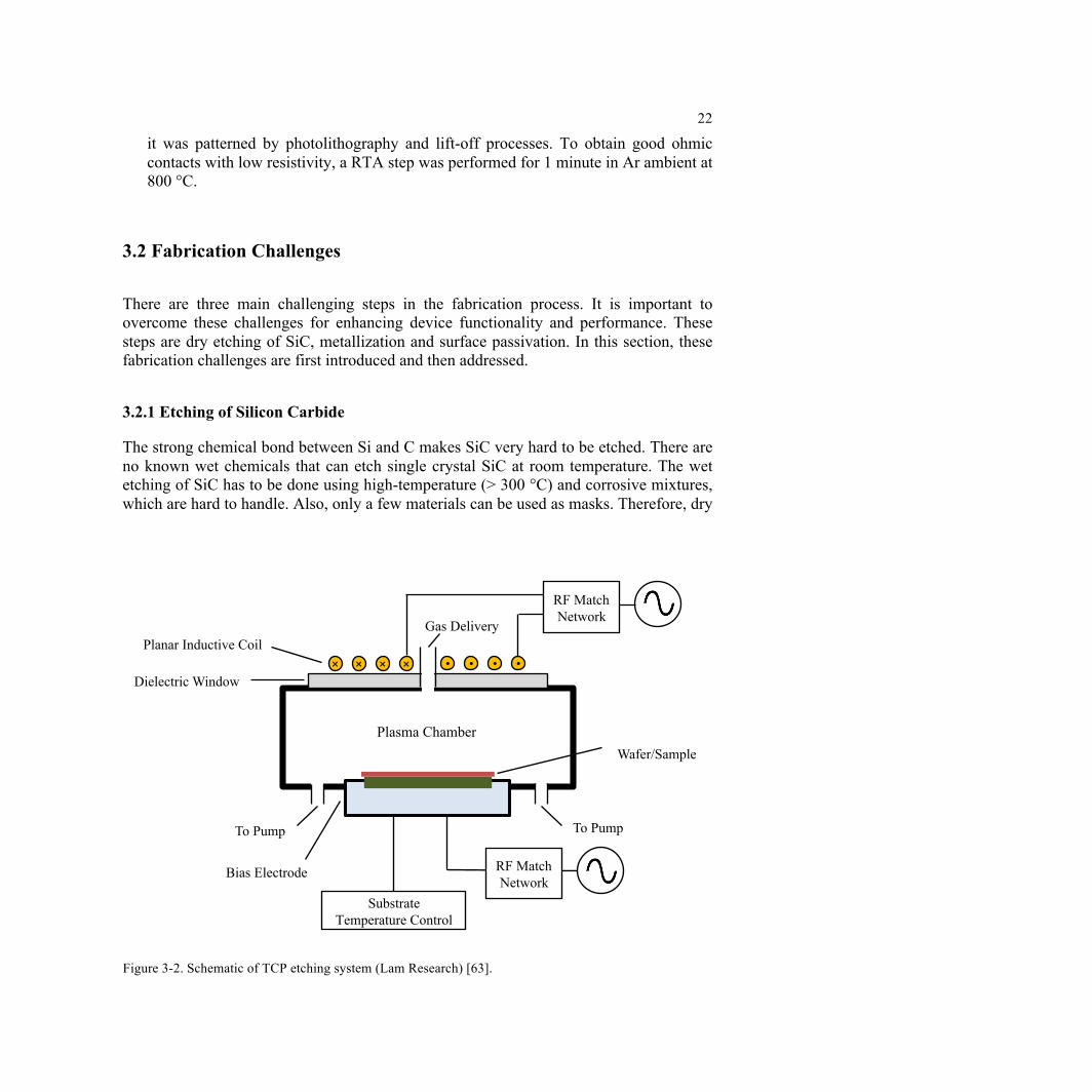
3.2.1 Etching of Silicon Carbide
The strong chemical bond between Si and C makes SiC very hard to be etched. There are no known wet chemicals that can etch single crystal SiC at room temperature. The wet etching of SiC has to be done using high-temperature (> 300 °C) and corrosive mixtures, which are hard to handle. Also, only a few materials can be used as masks. Therefore, dry
Figure 3-2. Schematic of TCP etching system (Lam Research) [63].
Planar Inductive Coil
Dielectric Window
Bias Electrode
Wafer/Sample
Substrate Temperature Control
RF Match Network
! • ! ! ! • • •
RF Match Network
Plasma Chamber
Gas Delivery
To Pump To Pump
23
etching is the commonly used method to pattern SiC to fabricate SiC electronic devices. In the early years, reactive ion etching (RIE) was commonly used to etch SiC using
fluorinated plasmas [57], [58]. However, rough surfaces were often observed due to the high dc self-bias. With the advent of high-density plasma etching systems, such as electron cyclotron resonance (ECR) etcher, and transformer/inductively coupled plasma (TCP/ICP) etcher, significant improvements of the etching rate and the etching profile of SiC materials were obtained [59]-[62]. The key advantage of these high-density plasma systems is the decoupling of ion density and ion energy. In a TCP/ICP etcher, the high-density plasmas are generated by an inductive coil where RF power is applied. For TCP etchers, the inductive coils are mounted on the top of the plasma chamber. Whereas for ICP etchers, the inductive coils are mounted on the outside of the chamber. The ion energy is controlled by a separate RF power source that is connected to the wafer platen. Therefore, high-density and low-energy ion flux can be obtained, which is expected to achieve high etch rates and low surface damage at the same time. In this work, a TCP etcher from Lam Research is used. A schematic of the TCP etching system is shown in Figure 3-2.
Conventional mask materials for dry etching, such as hard-baked photoresist, SiO2 and silicon nitride (Si3N4), are usually etched at higher rates than SiC in fluorine-based plasma chemistries. This is the reason why metal mask was used in some SiC etching processes. However, the residual metal leads to contamination in the subsequent process steps. As a result, etching process using a metal mask is not allowed in most laboratories. In addition, it has also been observed that due to sputtering of metal material onto the surface of SiC sample, grass-like structures are formed during the etching process. This is known as the micromasking phenomenon. Hence, it is of great importance to develop a
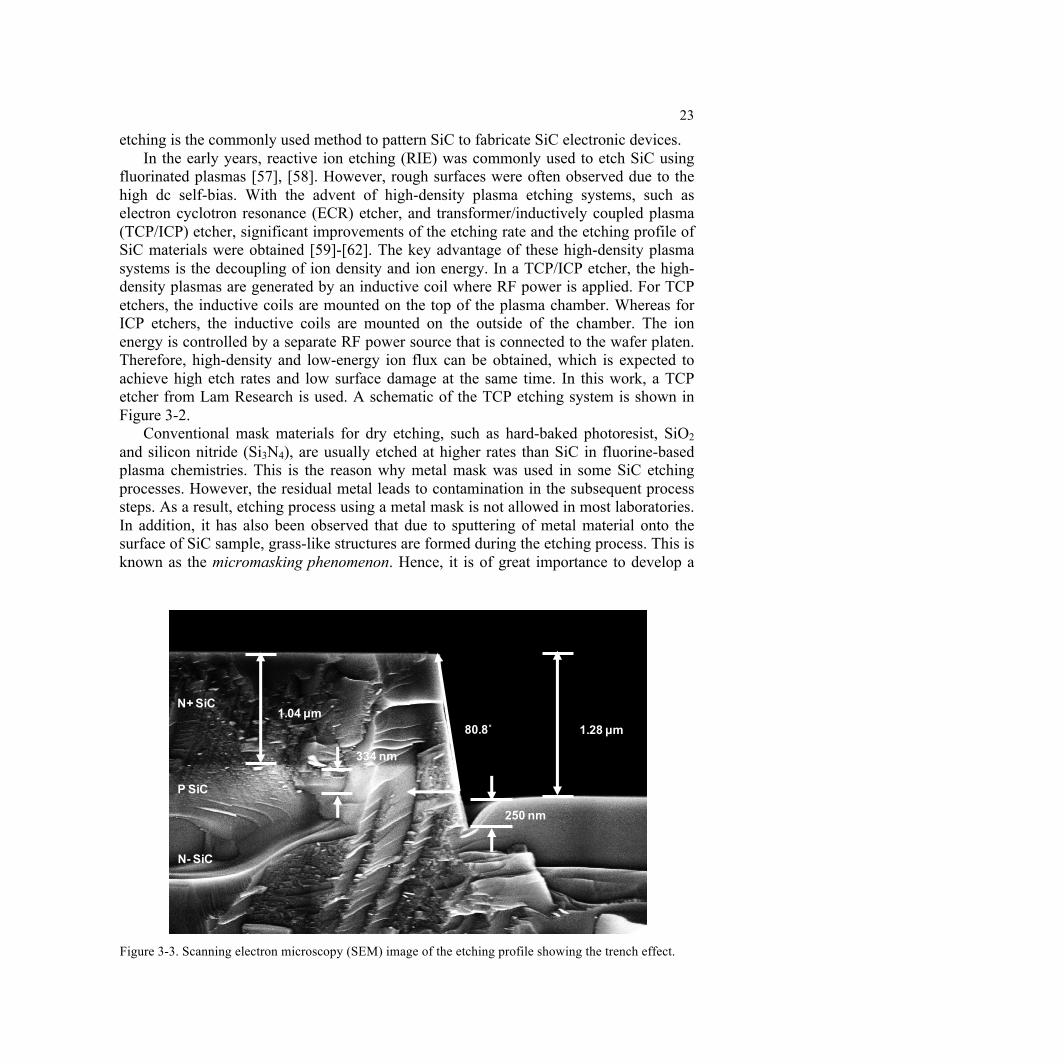
Figure 3-3. Scanning electron microscopy (SEM) image of the etching profile showing the trench effect.
80.8˚ 1.28 µm1.04 µm
334 nm
250 nm
N+ SiC
P SiC
N- SiC

24
dry etching process with high selectivity and nonmetallic mask. Hydrogen bromide (HBr) and chlorine (Cl2) based dry etching chemistry has been widely used to etch Si material with high etch rate and high selectivity to SiO2. Therefore, HBr and Cl2 based chemistry is studied to etch SiC using SiO2 as the mask material in this work. By changing the percentage of Cl2 in the gas mixture, different etch rate, selectivity and etch profile can be obtained. Based on the previous study of dry etching of polycrystalline 3C-SiC by Gao et al. [61], [62], two etching recipes for crystalline 4H-SiC have been developed and tested. One common problem of TCP etching of SiC material is the so-called trench effect, which occurs at the bottom of the etched features along the sidewalls. The scanning electron microscopy (SEM) image of the etching profile in Recipe 1 is shown in Figure 3-3. Though a considerably high etch rate of about 120 nm/minute, a high selectivity of 2.3:1 and a profile angle of 80.8° have been achieved, the trench effect cannot be ignored. As shown in Figure 3-3, a trench of 250 nm in depth is observed after the crystalline SiC material has been etched for 1.28 µm. This recipe is preferred in many MEMS process due to the high etch rate and steep profile angle, but the deep trenches will cause many problems in electronic devices. Recipe 2 is then developed for fabricating SiC electronic devices. In Recipe 2, the gas flow of Cl2 is reduced to 0, which completely removes the trenches. The SEM image of the etching profile using Recipe 2 is shown in Figure 3-4. An etch rate of around 90 nm/minute, a high selectivity of 3:1 and a profile angle of 72° have been achieved using Recipe 2. The two etching recipes are summarized in Table 3-1. As mentioned in the previous section, no etch stop layers exist in between different epitaxial 4H-SiC layers. The etching thickness is controlled by doing a timed etch. Therefore, an etch rate of about 90nm/minutes is preferred though a higher etch rate can be obtained by using a higher bias power.
Figure 3-4. SEM image of the etching profile without trench effect.
72.0˚ 1.18 µmN+ SiC
P SiC
N- SiC
N+ SiC

25
3.2.2 Metallization
For SiC-based devices, one of the critical challenges is to develop chemically and electrically stable ohmic contacts with low electrical resistance. Some important factors need to be taken into consideration, such as surface preparation, choice of metal and annealing temperature. The quality of ohmic contacts is very important for the performance and operation of the devices at high temperature.
Surface preparation is required because the metal needs to be intimately in contact with the semiconductor. Therefore, the sample surface needs to be free of photoresist residue and native oxide. A descum process using oxygen (O2) plasma was performed after developing exposed photoresist to eliminate any residual scum. Then the sample was dipped in buffered hydrogen fluoride solution for 30 seconds right before it was sent into the chamber for metal deposition. There are different techniques for depositing metal layers. E-beam evaporation is used in this work, which provides high deposition rate, precise control of film thickness and low as-deposited sheet resistance. Sputtering is an alternative option that has better step coverage and good adhesion of the metal to the substrate, but it is hard to precisely control the deposited film thickness. Lift-off process was used to pattern the metal contact. High temperature annealing process was performed at temperatures around 700 – 1050 °C in an oxygen-free ambient for reaction between metal and SiC to form silicides. The choices of metal and high temperature annealing condition are both critical for obtaining good ohmic contacts with low resistivity. For n-type SiC, Ni based metal stacks are commonly used and the typical specific contact resistance is in the range of 10-4 – 10-5 Ωcm2 [64]-[69]. For p-type SiC, the specific contact resistance is usually higher than that of n-type. Al based metal stacks are commonly used for p-type SiC and the typical specific contact resistance is in the range of 10-3 – 10-4 Ωcm2 [67]-[71].
Table 3-1. Summary of the etching recipes of crystalline 4H-SiC.
Recipe 1 Recipe 2
Chamber Pressure [mtorr] 12 12
TCP Source Power [W] 300 300
Bias Power [W] 150 150 Bottom Electrode Temperature [°C] 40 40 HBr Gas Flow Rate [sccm] 125 200
Cl2 Gas Flow Rate [sccm] 75 0
Etch Rate [nm/minute] ~ 120 ~ 90
Selectivity of SiC/SiO2 ~ 2.3:1 ~ 3:1
Profile Angle 81 72

26
Transfer Length Method (TLM)
For an ohmic contact with a total contact resistance of Rc, it is usually characterized by specific contact resistance ρc given by
!c = RcA, (3.1) where A is the contact area. The benefit of using ρc instead of Rc is the capability of evaluating contacts with different contact area.
Transfer length method (TLM) is widely used for the characterization of ohmic contacts. A typical TLM test structure consists of several contacts with unequal spacing between them. The total resistances between adjacent contacts are measured and have a linear dependence on the contact spacing. A schematic of a TLM test structure and a plot of total resistance as a function of contact spacing are shown in Figure 3-5 [72]. TLM test structures are fabricated on the same die together with SiC BJT devices.
For contacts with L ≥ 1.5LT, the total resistance RT between any two contacts can be expressed as
RT =RshdZ
+ 2Rc !RshZ
d + 2LT( ), (3.2)
where Rsh is the sheet resistance of the semiconductor, Z is the width of contacts, d is the spacing between any two adjacent contacts and LT is the transfer length that can be determined as the intercept value with x-axis in Figure 3-5. Rc can also be determined from the TLM measurement as the intercept value with y-axis:
Figure 3-5. Schematic of a transfer length method test structure and a plot of total resistance (RT) vs. contact spacing (d) [72].
MEASUREMENT TECHNIQUES 147
d4d3d2d1L
Z W
!
0 d
RT
2Rc
2LT
Slope = Rsh/Z
Fig. 3.22 A transfer length method test structure and a plot of total resistance as a function ofcontact spacing, d. Typical values might be: L = 50 µm, W = 100 µm, Z-W = 5 µm (should beas small as possible), d ! 5 to 50 µm.
The total resistance is measured for various contact spacings and plotted versus d asillustrated in Fig. 3.22. Three parameters can be extracted from such a plot. The slope!(RT )/!(d) = Rsh/Z leads to the sheet resistance with the contact width Z indepen-dently measured. The intercept at d = 0 is RT = 2Rc giving the contact resistance. Theintercept at RT = 0 gives "d = 2LT , which leads to the specific contact resistivity withRsh known from the slope of the plot. The transfer length method gives a complete char-acterization of the contact by providing the sheet resistance, the contact resistance, andthe specific contact resistivity.
The transfer length method is commonly used, but it has its own problems. Theintercept at RT = 0 giving LT is sometimes not very distinct, leading to incorrect "c
values. Perhaps a more serious problem is the uncertainty of the sheet resistance underthe contacts. Eq. (3.33) assumes the sheet resistance to be identical under the contactsand between contacts. But the sheet resistance under the contacts may differ from thesheet resistance between contacts due to the effects of contact formation. This would betrue for alloyed and silicided contacts where the region under the contact is modifiedduring contact fabrication, leading to the modified expression for the front contact andtotal resistance,66
Rcf = "c
LT kZcoth (L/LT k) (3.34)
and
RT = Rshd
Z+ 2Rc ! Rshd
Z+ 2RskLT k
Z= Rsh
Z[d + 2(Rsk/Rsh)LT k] (3.35)
where Rsk is the sheet resistance under the contact and LT k = ("c/Rsk)1/2. The slope of
the RT versus d plot still gives Rsh/Z and the intercept at d = 0 gives 2Rc. However, theintercept at RT = 0 now yields 2LT k(Rsk/Rsh) and it is no longer possible to determine "c
since Rsk is unknown. Nevertheless, by determining Rcf from the transfer length methodand Rce from the end resistance method, where
Rce =#
Rsk"c
Z sinh(L/LT k)= "c
ZLT k sinh(L/LT k);Rce
Rcf
= 1cosh(L/LT k)
(3.36)
27
RT (d = 0) = 2Rc = 2RshZLT . (3.3)
The sheet resistance can be obtained by solving Equation (3.3):
Rsh =RcZLT. (3.4)
The potential distribution under the contact is such that the voltage is the highest near the contact edge and drops nearly exponentially with distance. The transfer length LT is defined as the “1/e” distance of the voltage curve:
LT = !c / Rsh . (3.5) Thus, the specific contact resistance ρc can also be obtained by TLM:
!c = LT2 Rsh. (3.6)
Characterization Results for Ohmic Contacts
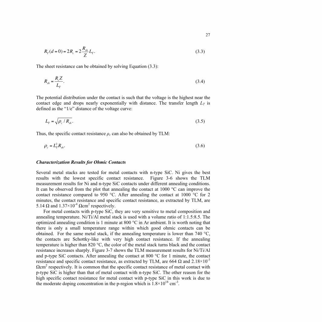
Several metal stacks are tested for metal contacts with n-type SiC. Ni gives the best results with the lowest specific contact resistance. Figure 3-6 shows the TLM measurement results for Ni and n-type SiC contacts under different annealing conditions. It can be observed from the plot that annealing the contact at 1000 °C can improve the contact resistance compared to 950 °C. After annealing the contact at 1000 °C for 2 minutes, the contact resistance and specific contact resistance, as extracted by TLM, are 5.14 Ω and 1.37×10⁻⁴ Ωcm2 respectively.
For metal contacts with p-type SiC, they are very sensitive to metal composition and annealing temperature. Ni/Ti/Al metal stack is used with a volume ratio of 1:1.5:8.5. The optimized annealing condition is 1 minute at 800 °C in Ar ambient. It is worth noting that there is only a small temperature range within which good ohmic contacts can be obtained. For the same metal stack, if the annealing temperature is lower than 740 °C, the contacts are Schottky-like with very high contact resistance. If the annealing temperature is higher than 820 °C, the color of the metal stack turns black and the contact resistance increases sharply. Figure 3-7 shows the TLM measurement results for Ni/Ti/Al and p-type SiC contacts. After annealing the contact at 800 °C for 1 minute, the contact resistance and specific contact resistance, as extracted by TLM, are 664 Ω and 2.18×10⁻³ Ωcm2 respectively. It is common that the specific contact resistance of metal contact with p-type SiC is higher than that of metal contact with n-type SiC. The other reason for the high specific contact resistance for metal contact with p-type SiC in this work is due to the moderate doping concentration in the p-region which is 1.8×1018 cm-3.

28
Figure 3-7. TLM measurement results for Ni/Ti/Al and p-type SiC contacts.
Figure 3-6. TLM measurement results for Ni and n-type SiC contacts under different annealing conditions.
Rc=664ΩSpecific Rc=2.18×10⁻³Ωcm2
Sheet Resistance=20.2kΩ/☐
Rc=7.60ΩSpecific Rc=2.84×10⁻⁴Ωcm2
Sheet Resistance=20.34Ω/☐
Rc=5.14ΩSpecific Rc=1.37×10⁻⁴Ωcm2
Sheet Resistance=19.22Ω/☐
29
3.2.3 Surface Passivation
Dielectrics are needed for surface passivation of SiC devices as well as for gate dielectric layers of metal-oxide-semiconductor field effect transistors (MOSFETs). SiO2 is an attractive dielectric for SiC devices due to the fact that it can be formed simply by thermal oxidation of SiC. However, improving the quality of the dielectric is still a challenging issue despite of significant progress in recent years.
Two possible chemical reactions are proposed for thermal oxidation of SiC at the interface [1]:
SiC + 32
O2 ! SiO2 + CO, (3.1)
SiC + O2 ! SiO2 + C. (3.2)
The thermal oxidation of SiC shows lower oxidation rate and needs higher temperature compared with Si due to the strong bond between Si and C. The oxidation rate is higher for C face compared with Si face [73]. But the oxide grown on the Si face is usually better in terms of electrical quality. Therefore, Si face is preferred for building devices. Unlike Si, one of the concerns of the thermal oxidation of SiC is the excess carbon. Though most of the carbon is removed during the oxidation process as CO gas, carbon clusters could still form at the SiO2/SiC interface, which seriously degrade the quality of the dielectric layer [74]. This problem is more noticeable in 4H-SiC than in 6H-SiC [75], [76], [81].
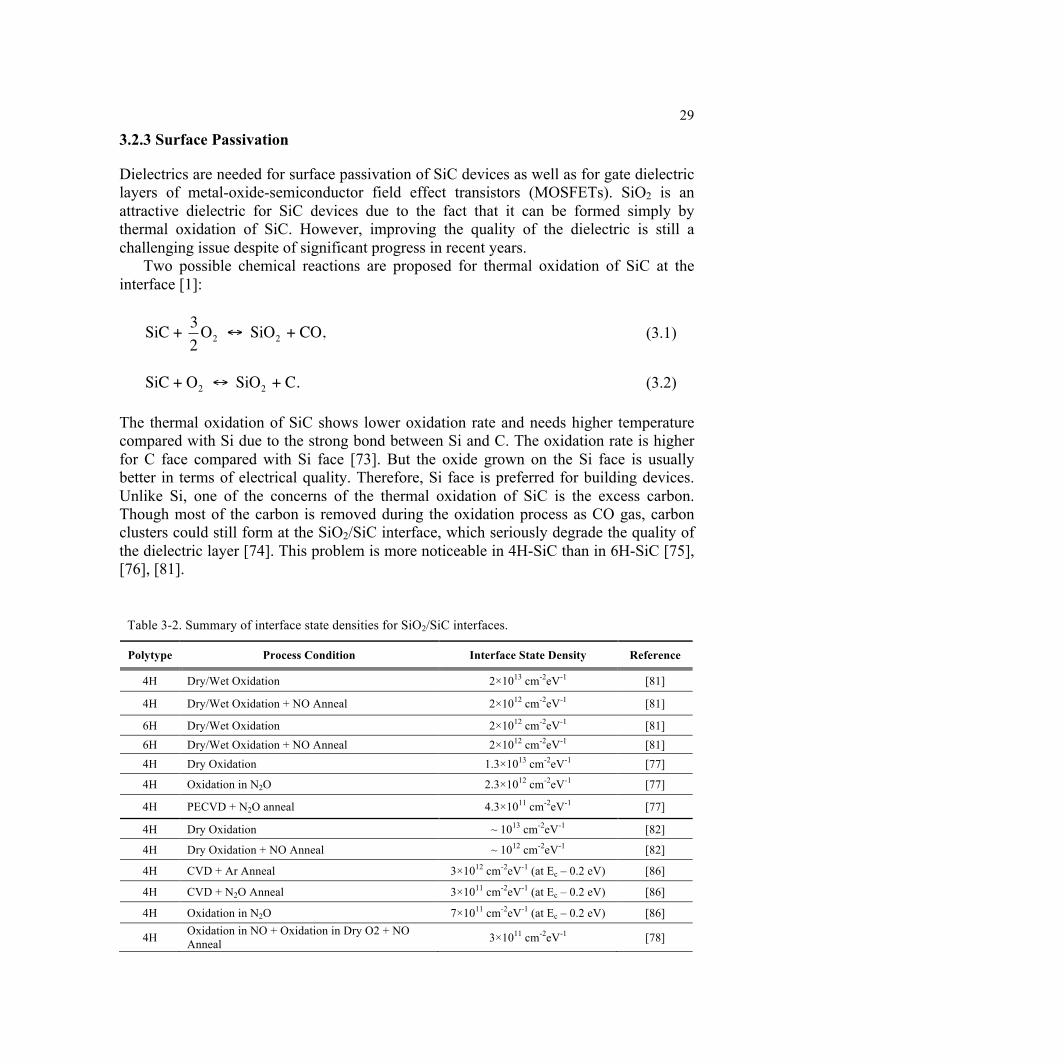
Table 3-2. Summary of interface state densities for SiO2/SiC interfaces.
Polytype Process Condition Interface State Density Reference
4H Dry/Wet Oxidation 2×1013 cm-2eV-1 [81]
4H Dry/Wet Oxidation + NO Anneal 2×1012 cm-2eV-1 [81]
6H Dry/Wet Oxidation 2×1012 cm-2eV-1 [81] 6H Dry/Wet Oxidation + NO Anneal 2×1012 cm-2eV-1 [81] 4H Dry Oxidation 1.3×1013 cm-2eV-1 [77]
4H Oxidation in N2O 2.3×1012 cm-2eV-1 [77]
4H PECVD + N2O anneal 4.3×1011 cm-2eV-1 [77]
4H Dry Oxidation ~ 1013 cm-2eV-1 [82]
4H Dry Oxidation + NO Anneal ~ 1012 cm-2eV-1 [82]
4H CVD + Ar Anneal 3×1012 cm-2eV-1 (at Ec – 0.2 eV) [86]
4H CVD + N2O Anneal 3×1011 cm-2eV-1 (at Ec – 0.2 eV) [86]
4H Oxidation in N2O 7×1011 cm-2eV-1 (at Ec – 0.2 eV) [86]
4H Oxidation in NO + Oxidation in Dry O2 + NO Anneal 3×1011 cm-2eV-1 [78]
30
Many efforts have been made to improve the quality of the SiO2/SiC interface. One promising method to reduce the density of interface states is nitridation of the oxide. This can be done by thermally growing the oxide in nitric oxide (NO) or nitrous oxide (N2O) [77]-[79], annealing the thermally grown oxide in NO or N2O [77], [81]-[85], or annealing the deposited oxide in NO or N2O [77], [86], [87]. According to the work by Jamet et al., nitridation process can provide critical improvements on the quality of SiO2/SiC interface because: 1) NO and N2O are able to passivate the dangling Si bonds and replace the strained bonds with S≡N bonds, and 2) NO and N2O can help to remove the excess carbon and associated silicon-oxycarbon bonds from the interface [88]. The interface state density of the SiO2/SiC interface has been studied and characterized by many research groups, and the results are summarized in Table 3-2. The numerical and experimental characterization shows that the profile of interface state density usually exponentially increases at the conduction band edge and the valence band edge [89], [90]. The typical interface state density in SiC devices ranges from 1011 to 1013 cm-2eV-1. The number is much higher compared with Si devices, which is on the order of 1010 cm-2eV-1. More investigation into improving the interface quality is still urgently needed for SiC devices.
For SiC BJTs, the quality of the interface between SiC and the surface passivation layer has a significant impact on the device performance, especially on current gain. This is because the recombination current caused by interface traps at the extrinsic base surface and along the base-emitter junction sidewall can be a main component of the base current. By reducing the density of interface traps, the recombination current caused by interface traps is reduced. Therefore, the base transport factor αT is increased and higher current gain can be achieved. Due to the limitation of the highest temperature allowed in the furnaces, PECVD oxide without high temperature annealing is used in this work. The impact of the interface traps on the current gain is discussed in Chapter 4.
3.3 Conclusions
In this chapter, the baseline six-mask microfabrication process for SiC BJTs is presented. Several key steps in the fabrication process flow are discussed. For the etching process of SiC, TCP etching was employed using SiO2 as the mask material. In order to avoid the trenching effect, HBr and Cl2 based etching chemistry was studied. Good sidewall profile and high selectivity were obtained by using the optimized recipe. Metallization process was also studied because the quality of ohmic contacts is very important for the performance and operation of the devices. Ni was used for n-type SiC contacts and Ni/Ti/Al metal stack was used for p-type SiC contacts. High temperature annealing process was optimized for getting good ohmic contacts. The contacts were characterized using transfer length method. Some issues with the surface passivation method were addressed and discussed. Carbon clusters could form at the SiO2/SiC interface during the oxidation process, which severely degrade the quality of the dielectric layer. Though nitridation of the oxide has been proved to be effective in reducing the interface state

31
density, more investigations into improving the interface quality are needed. These fabrication processes are employed to manufacture the SiC BJTs presented in Chapter 4.

32
Chapter 4 Simulation and Characterization Results of 4H-SiC Bipolar Junction Transistors
There are growing interests on developing high temperature integrated circuit using SiC BJTs. This is because the superior material properties of SiC allow SiC based semiconductor devices to be functional at extremely high temperatures. Also, SiC BJTs are not as strongly affected by oxide quality as SiC MOSFETs. Additionally, SiC BJTs are normally-off devices and have higher transconductance compared with SiC JFETs. In this chapter, design, characterization and simulation results of 4H-SiC BJTs are discussed. The device was first characterized at room temperature. Then high temperature characterization was performed. Comprehensive characterization including current gain, early voltage and intrinsic voltage gain are described. It has been found that the current gain of the device is reduced at elevated temperature. On the other hand, the output resistance increases when temperature rises. The intrinsic voltage gain is higher at 400 °C compared with at room temperature, suggesting 4H-SiC BJT has the potential to be used as a voltage amplifier at extremely high temperatures. The high temperature effects in 4H-SiC are studied to explain the high temperature performance of the device. The effects of SiC/SiO2 interface traps on the electrical characteristics of SiC BJTs are also discussed.
4.1 Device Structure
The schematic cross-sectional illustration of the 4H-SiC BJT is shown in Figure 4-1 (a). The structure has 5 epitaxial layers grown on a 4° off-axis Si-face n-type 4H-SiC wafer. The emitter region is formed by a 1-µm-thick N+ 4H-SiC epitaxial layer doped at 1019 cm-3, the base region is formed by a 0.3-µm-thick P-type epitaxial layer doped at 1.8×1018 cm-3, and the collector region is formed by a 1-µm-thick N- epitaxial layer doped at 1016 cm-3. The highly doped N+ epitaxial layer under the N- collector is the sub-collector region, which is used to form the collector contact on the topside of the structure. Finally, the P+ region grown on the 4H-SiC substrate enables junction isolation for
(b)

33
separate BJT devices. Figure 4-1 (b) shows the schematic top view of the device. By having all the metallic contacts at the top of the structure, the proposed BJT can be easily integrated into large-scale circuits for sensing applications. It is also worth noticing that the device has two base contact regions. As discussed in Chapter 3, the metal contact with p-type SiC has higher contact resistance compared with the metal contact with n-type SiC. By having double base contacts, the contact resistance can be reduced.
The thickness and doping concentration of the epitaxial layers are designed to have high current gain β and high output resistance ro. This is because the devices developed in this work are used for high temperature sensing applications that usually require low voltage, analog integrated circuits.
Figure 4-1. (a) Cross-sectional schematic and (b) schematic top view of the 4H-SiC BJT. The red line in (b) indicates the position of the cross-section in (a).
P+ Isolation Layer
1.0 µm N+ Sub-collector
1.0 µm N- Collector 0.3 µm P Base 1.0 µm N+ Emitter
Emitter Contact Base Contact
Collector Contact
Passivation Layer
WE WB WC
N+ 4H-SiC Substrate
EmitterContact
Base Contact
CollectorContact
(a)
(b)

34
As we have discussed in Chapter 1, the operating mechanism of bipolar junction transistors is quite complicated. In order to get a simplified expression for the current gain β, several assumptions have to be made: 1) the epitaxial layers are nondegenerate and uniformly doped; 2) the transistor is under steady-state condition; 3) low-level injection prevails in the quasineutral regions; 4) there is no photogeneration in the semiconductor regions; 5) thermal generation and recombination can be ignored in the depletion regions; 6) the quasineutral widths of the emitter and collector are greater than the minority carrier diffusion lengths in these regions; 7) WB/LB << 1. The current gain β of a NPN BJT can be derived as
! =1
DE
DB
NB
NE
WB
LE+12WB
LB
!
"#
$
%&
2 , (4.1)
where DB is the diffusion coefficient of electrons in the base region and DE is the diffusion coefficient of holes in the emitter region, NB and NE are the effective doping concentrations in the base and emitter regions, LB is the diffusion length of electrons in the base region and LE is the diffusion lengths of holes in the emitter region, WB is the width of the base region. For the emitter region, a heavily doped emitter with the emitter width greater than the diffusion length of the minority carrier is desired. Combined with fabrication considerations, the emitter doping concentration is set at 1019 cm-3, and the emitter width is chosen to be 1 µm. Also, a lightly doped base region with thin base width is preferred for improving the current gain.
The base width WB changes with the applied voltages. This phenomenon is known as base width modulation effect or early effect. The output resistance ro can be calculated by
ro = VA +VCE( ) / IC, (4.2)
where VA is the early voltage, VCE is the applied voltage between the collector and the emitter, and IC is the current flowing through the collector under DC bias. In order to get high output resistance, low collector doping and high base doping are required. Also, the width of the collector region should be greater than the diffusion length of the minority carriers, while the base width should be as wide as possible. In this work, the collector doping concentration is 1016 cm-3, and the collector width is 1 µm. It is worth noting that there are trade-offs for the design of the base region. A base doping of 1.8×1018 cm-3 was used to get a high output resistance. Additionally, this doping concentration allows good ohmic contact to the base layer without an ion implantation process. A thin base of 0.3 µm was utilized for a higher current gain. Figure 4-2 is a scanning electron microscopy (SEM) image of the cross-sectional view showing the thickness of each epitaxial layer. Figure 4-3 shows the SEM image of the fabricated device. The dimension of the emitter region is 60 µm × 100 µm.

35
Figure 4-2. SEM image of the cross-section view showing the thickness of each epitaxial layer.
Figure 4-3. SEM image of the fabricated 4H-SiC BJT.
1.04 µm334 nm
N+ Emitter
P Base
N- Collector
N+ Sub-collector
P+ Isolation
1.02 µm
1.07 µm
1 µm4H-SiC
100 μm
EmitterPad
Emitter
BaseCollector
BasePad
CollectorPad
36
4.2 Room Temperature Characterization of the 4H-SiC BJT
The fabricated 4H-SiC BJT was first characterized at room temperature. Figure 4-4 shows the forward output characteristics of the device at 20 °C. While taking this measurement, the emitter is grounded. Different base currents from 0 µA to 200 µA with a 50 µA step were applied. At each base current, the collector voltage is swept from 0 V to 15 V. The dark cyan line in Figure 4-4 shows the collector current (IC) vs. collector-emitter voltage (VCE) curve at IB = 0 µA. A high transconductance (Gm) of 56 mS was reached at IC = 1.4 mA, and the output resistance ro was extracted to be 50 kΩ. The intrinsic voltage gain (Av), which is the product of Gm and ro, is 2800 under room temperature at IC = 1.4 mA and IB = 200 µA.
Figure 4-5 depicts the Gummel plot and the current gain (β) vs. base-emitter voltage (VBE) curve under room temperature. The emitter was grounded when this measurement was taken. Also, the base voltage and collector voltage simultaneously increased from 0 to 20 volts. The base-collector junction is zero biased for all the measurements, i.e. VCB = 0 V. The current gain increases with VBE, and the maximum value of the current gain is 12.4 at room temperature.
4.3 High Temperature Effects in 4H-SiC
To understand the device behavior at elevated temperatures, the high temperature effects on basic semiconductor physical properties need to be studied. As discussed in Chapter 2, nearly all the properties of semiconductors can change with temperature. For 4H-SiC BJTs, there are two effects that have the greatest impacts on the device performance. One is the incomplete ionization effect, which determines the carrier concentration in the semiconductor. The other one is the temperature dependence of the carrier lifetime.
4.3.1 Temperature Dependence of Carrier Concentration
For an extrinsic semiconductor (doped semiconductor), the carrier concentrations in the semiconductor are mainly controlled by the ionized impurity concentration and the intrinsic carrier concentration. In Si, most impurity levels, like Boron (B) and Phosphorus (P), are shallow enough so that the dopants can be considered fully ionized at room temperature. As discussed in Chapter 2, the donor level (ED) for nitrogen (N) and acceptor level (EA) for aluminum (Al) in SiC are relatively deep compared to the thermal energy kT. For 4H-SiC, a single donor level, ED = 65 meV below the conduction band edge is assumed after simplification, and an acceptor energy level is EA = 191 meV above the valence band edge. Therefore, the dopants cannot be considered fully ionized at room temperature and the concentration of the ionized dopants increases with rising temperature.
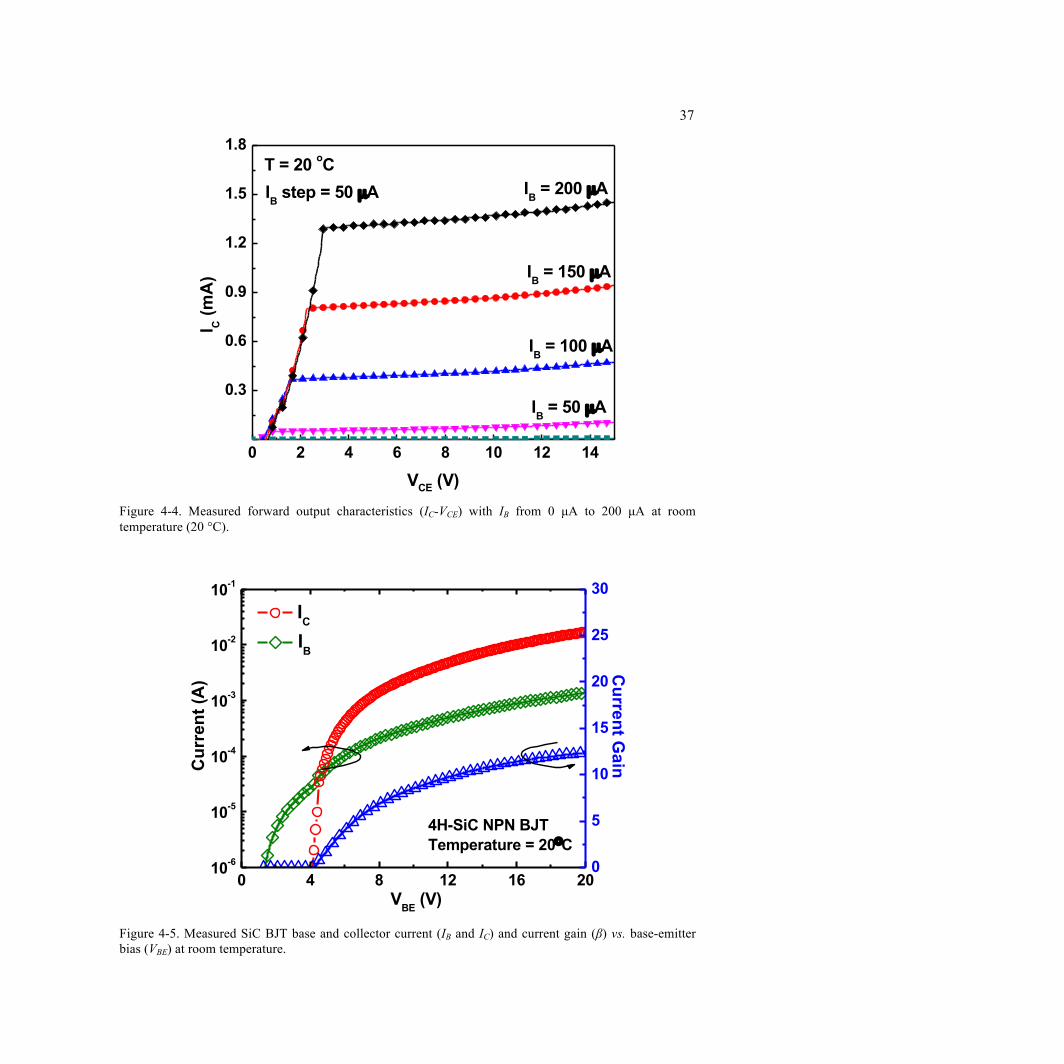
37
Figure 4-4. Measured forward output characteristics (IC-VCE) with IB from 0 µA to 200 µA at room temperature (20 °C).
Figure 4-5. Measured SiC BJT base and collector current (IB and IC) and current gain (β) vs. base-emitter bias (VBE) at room temperature.
0 2 4 6 8 10 12 140.0
0.3
0.6
0.9
1.2
1.5
1.8
IB = 50 µA
IB = 100 µA
IB = 150 µA
IB = 200 µAIB step = 50 µAT = 20 oC
I C (m
A)
VCE (V)
0 4 8 12 16 2010-6
10-5
10-4
10-3
10-2
10-1
IC IB
VBE (V)
Cur
rent
(A)
4H-SiC NPN BJTTemperature = 20°C
0
5
10
15
20
25
30
Current G
ain
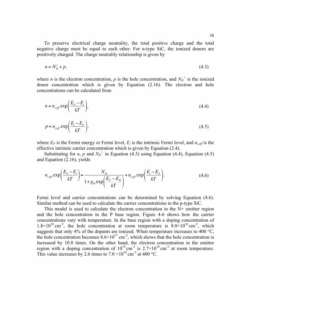
38
To preserve electrical charge neutrality, the total positive charge and the total negative charge must be equal to each other. For n-type SiC, the ionized donors are positively charged. The charge neutrality relationship is given by
n = ND
+ + p, (4.3) where n is the electron concentration, p is the hole concentration, and ND
+ is the ionized donor concentration which is given by Equation (2.16). The electron and hole concentrations can be calculated from
n = ni,eff expEF !Ei
kT"
#$
%
&', (4.4)
p = ni,eff expEi !EF
kT"
#$
%
&', (4.5)
where EF is the Fermi energy or Fermi level, Ei is the intrinsic Fermi level, and ni,eff is the effective intrinsic carrier concentration which is given by Equation (2.4).
Substituting for n, p and ND+ in Equation (4.3) using Equation (4.4), Equation (4.5)
and Equation (2.16), yields
ni,eff expEF !Ei
kT"
#$
%
&'=
ND
1+ gD expEF !ED
kT"
#$
%
&'+ ni,eff exp
Ei !EF
kT"
#$
%
&'. (4.6)
Fermi level and carrier concentrations can be determined by solving Equation (4.6). Similar method can be used to calculate the carrier concentrations in the p-type SiC.
This model is used to calculate the electron concentration in the N+ emitter region and the hole concentration in the P base region. Figure 4-6 shows how the carrier concentrations vary with temperature. In the base region with a doping concentration of 1.8×1018 cm-3, the hole concentration at room temperature is 8.0×1016 cm-3, which suggests that only 4% of the dopants are ionized. When temperature increases to 400 °C, the hole concentration becomes 8.6×1017 cm-3, which shows that the hole concentration is increased by 10.8 times. On the other hand, the electron concentration in the emitter region with a doping concentration of 1019 cm-3 is 2.7×1018 cm-3 at room temperature. This value increases by 2.6 times to 7.0 ×1018 cm-3 at 400 °C.
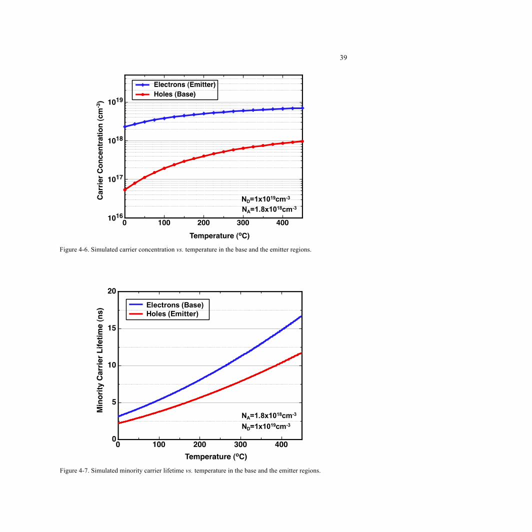
39
Figure 4-6. Simulated carrier concentration vs. temperature in the base and the emitter regions.
Figure 4-7. Simulated minority carrier lifetime vs. temperature in the base and the emitter regions.
NA=1.8x1018cm-3ND=1x1019cm-3
NA=1.8x1018cm-3
ND=1x1019cm-3
Electrons (Base)Holes (Emitter)

40
4.3.2 Temperature Dependence of Carrier Lifetime
The minority carrier lifetimes in 4H-SiC depend on temperature and doping level, which can be modeled by Equation (2.20). The carrier lifetimes increase exponentially with rising temperature. The mechanism is still unknown and there is limited study on this topic. The parameters for the temperature dependence are taken from [41] and [50]. Figure 4-7 shows the simulation results on the temperature dependence of the minority carrier lifetimes in the base and emitter regions when τmax
n,p = 10 ns. In the base region, the minority carrier lifetime (electron lifetime) increases from 3.5 ns at room temperature to 14.8 ns at 400 °C. In the emitter region the minority carrier lifetime (hole lifetime) increases from 2.5 ns at room temperature to 10.4 ns at 400 °C. At a given temperature, the electron lifetime in the emitter region is lower than the hole lifetime in the base region due to higher doping concentration in the N+ emitter.
4.4 High Temperature Characterization of 4H-SiC BJTs
The fabricated device was characterized at elevated temperatures using a high temperature probe station made by Signatone together with an Agilent B2912A Precision Source/Measurement Unit. The high temperature probe station is shown in Figure 4-8. It consists of a ceramic hot chuck, a temperature controller and a water cooler. Figure 4-9 shows the forward output characteristics of the 4H-SiC BJT with IB from 0 µA to 600 µA
Figure 4-8. High temperature probe station made by Signatone.
High Temperature Probe Station
Temperature Controller
Water Cooler
Ceramic Hot Chuck
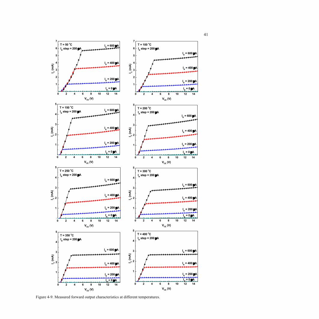
41
Figure 4-9. Measured forward output characteristics at different temperatures.
0 2 4 6 8 10 12 140
1
2
3
4
5
6
7
IB = 0 µA
IB = 200 µA
IB = 400 µA
IB = 600 µAIB step = 200 µAT = 50 oC
I C (m
A)
VCE (V)0 2 4 6 8 10 12 14
0
1
2
3
4
5
6
7
IB = 0 µA
IB = 200 µA
IB = 400 µA
IB = 600 µAIB step = 200 µAT = 100 oC
I C (m
A)
VCE (V)
0 2 4 6 8 10 12 140
1
2
3
4
5
IB = 0 µA
IB = 200 µA
IB = 400 µA
IB = 600 µAIB step = 200 µAT = 150 oC
I C (m
A)
VCE (V)0 2 4 6 8 10 12 14
0
1
2
3
4
5
IB = 0 µA
IB = 200 µA
IB = 400 µA
IB = 600 µAIB step = 200 µAT = 200 oC
I C (m
A)
VCE (V)
0 2 4 6 8 10 12 140
1
2
3
4
5
IB = 0 µA
IB = 200 µA
IB = 400 µA
IB = 600 µAIB step = 200 µAT = 250 oC
I C (m
A)
VCE (V)0 2 4 6 8 10 12 14
0
1
2
3
4
5
IB = 0 µA
IB = 200 µA
IB = 400 µA
IB = 600 µA
IB step = 200 µAT = 300 oC
I C (m
A)
VCE (V)
0 2 4 6 8 10 12 140
1
2
3
4
5
IB = 0 µA
IB = 200 µA
IB = 400 µA
IB = 600 µA
IB step = 200 µAT = 350 oC
I C (m
A)
VCE (V)
0 2 4 6 8 10 12 140
1
2
3
4
5
IB = 0 µA
IB = 200 µA
IB = 400 µA
IB = 600 µA
IB step = 200 µAT = 400 oC
I C (m
A)
VCE (V)

42
Figure 4-10. Measured SiC BJT current gain vs. collector current at different temperatures (up to 400 °C).
Figure 4-11. Measured SiC BJT early voltage (VEA) and output resistance (ro) vs. temperature; the inset illustrates the base width (WB) widening effect at elevated temperatures.
10-5 10-4 10-3 10-2 10-10
3
6
9
12
15
18
6.7
Cur
rent
Gai
n
IC (A)
20 50 100 150 200 250 300 350 400
Temperature (°C) 14.5
VBC = 0V
0 100 200 300 4000
50
100
150
200
250
300
350
Temperature (°C)
10
100
1k
WB as T
VCE = 15V
Early
Vol
tage
(V)
Output R
esistance (KΩ
)

43
with a 200 µA step over a temperature range from 50 °C to 400 °C. The device shows stable operation over the entire temperature range. At the same base current, the collector current decreases with increasing temperature, which corresponds to lower current gain at elevated temperatures. In addition, the slopes of the collector current curves in the saturation region decrease with rising temperature, which corresponds to higher output resistance at elevated temperatures.
The plot of current gain (β) vs. collector current (IC) at different temperatures is shown in Figure 4-11. The maximum β degrades from 14.5 at 20 °C to 6.7 at 400 °C. The two high temperature effects discussed in Section 4.3 have the greatest impacts on the high temperature performance of the device. They compete with each other for the change of the current gain with rising temperature. One effect is the temperature dependence of carrier concentration. Due to the incomplete ionization effect, the impurities are only partially ionized at relatively low temperatures. Thus, the carrier concentration increases with increasing temperature as more dopants are ionized. As calculated in Section 4.3.1, only 4% of the acceptors are ionized under room temperature in the base region, and the hole concentration is increased by 10.8 times at 400 °C. On the other hand, the electron concentration in the emitter region increases by only 2.6 times at 400 °C compared with the value at room temperature. From Equation (4.1), it can be seen that higher NB/NE value at high temperature will end up with lower β. The other effect is the temperature dependence of carrier lifetime. The minority carrier lifetimes in the base and emitter regions increase exponentially with rising temperature. Since the diffusion length L is proportional to !, LE and LB increase when temperature goes up. Thus, β increases with increasing temperature as indicated in Equation (4.1). Since the degradation of current gain with increasing temperature up to 400 °C was observed in the measurement results, the incomplete ionization effect is believed to play a more important role at high temperatures.
To comprehensively evaluate the device’s performance for high temperature sensing applications, more characterization was performed. Figure 4-11 illustrates that the early voltage and output resistance of the device increase with rising temperature. This is because both the equivalent base doping concentration and base width increase with temperature. The intrinsic voltage gain (Av) vs. temperature is plotted in Figure 4-12. Av is calculated when IB = 200 µA at all the temperatures. Av first decreases from 3300 at 20 °C to 837 at 250 °C due to transconductance (Gm) degradation, then it increases rapidly to 5900 at 400 °C due to the enhancement in output resistance (ro). The result shows that the device has even higher intrinsic voltage gains at high temperatures, which demonstrates the potential of 4H-SiC BJTs to be used as voltage amplifiers at extremely high temperatures.

44
4.5 Effects of SiC/SiO2 Interface Traps
As discussed in Section 3.2.3, the quality of the interface between SiC and the surface passivation layer has a significant impact on the device performance of 4H-SiC BJTs, especially on the current gain. This is because the recombination current caused by
Figure 4-12. Measured SiC BJT voltage gain (Av) vs. temperature.
Figure 4-13. Schematic cross-sectional view of the 4H-SiC BJT presenting where the interface traps physically reside in the device.
0 100 200 300 400
103
104
VEA(ro) enhancement
5900
3300
VCE = 15V
Temperature (°C)
Volta
ge G
ain
(Av)
Gm degradation
Base
Emitter
Emitter Contact
Base Contact
Interface Traps
P Base N+ Emitter Metal Contact
SiO2
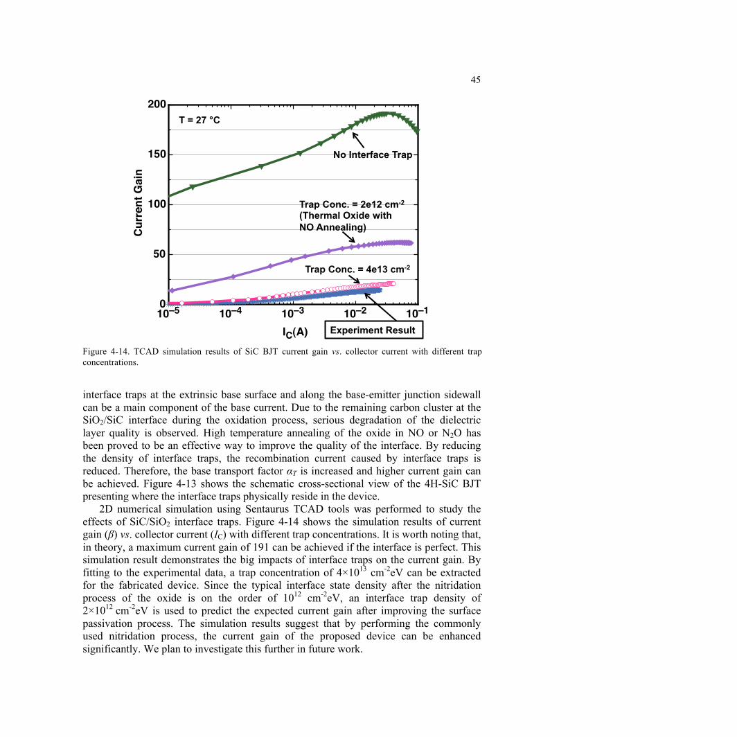
45
interface traps at the extrinsic base surface and along the base-emitter junction sidewall can be a main component of the base current. Due to the remaining carbon cluster at the SiO2/SiC interface during the oxidation process, serious degradation of the dielectric layer quality is observed. High temperature annealing of the oxide in NO or N2O has been proved to be an effective way to improve the quality of the interface. By reducing the density of interface traps, the recombination current caused by interface traps is reduced. Therefore, the base transport factor αT is increased and higher current gain can be achieved. Figure 4-13 shows the schematic cross-sectional view of the 4H-SiC BJT presenting where the interface traps physically reside in the device.
2D numerical simulation using Sentaurus TCAD tools was performed to study the effects of SiC/SiO2 interface traps. Figure 4-14 shows the simulation results of current gain (β) vs. collector current (IC) with different trap concentrations. It is worth noting that, in theory, a maximum current gain of 191 can be achieved if the interface is perfect. This simulation result demonstrates the big impacts of interface traps on the current gain. By fitting to the experimental data, a trap concentration of 4×1013 cm-2eV can be extracted for the fabricated device. Since the typical interface state density after the nitridation process of the oxide is on the order of 1012 cm-2eV, an interface trap density of 2×1012 cm-2eV is used to predict the expected current gain after improving the surface passivation process. The simulation results suggest that by performing the commonly used nitridation process, the current gain of the proposed device can be enhanced significantly. We plan to investigate this further in future work.
Figure 4-14. TCAD simulation results of SiC BJT current gain vs. collector current with different trap concentrations.
10–5 10–4 10–3 10–2 10–10
50
100
150
200
IC(A)
Cur
rent
Gai
nNo Interface Trap
Trap Conc. = 2e12 cm-2
(Thermal Oxide with NO Annealing)
Trap Conc. = 4e13 cm-2
Experiment Result
T = 27 °C
46
4.6 Conclusions
In this chapter, theoretical analysis, design and characterization of 4H-SiC NPN BJTs are presented. The device shows stable operation at high temperatures up to 400 °C. Comprehensive characterization including current gain, early voltage, and intrinsic voltage gain was performed. At elevated temperatures, although the current gain of the device is reduced, the output resistance increases. At 400 °C, an intrinsic voltage gain of 5900 is achieved, which is even higher than 3300 at room temperature. This phenomenon suggests that 4H-SiC BJT has the potential to be used as a voltage amplifier at extremely high temperatures. The high temperature effects of 4H-SiC are also studied. Higher current gain could be obtained if the surface passivation process is improved. This work shows that 4H-SiC BJT is a promising technology for harsh environment sensing applications.

47
Chapter 5 Fabrication and Characterization of SiC PN Diode for High Temperature Sensing Applications
Temperature sensing under extreme environments is important to various industrial applications. Among different types of temperature sensors, semiconductor diode sensors have the advantages of high sensitivity and compatibility with integrated circuits. Thanks to the superior material properties of SiC, semiconductor diodes made by SiC have been investigated as high temperature sensors. SiC Schottky diodes have been previously demonstrated as viable temperature sensors that can work up to 400°C [91]-[93]. However, SiC Schottky diode suffers from reliability issues of the Schottky contact as well as high leakage current at elevated temperatures. On the other hand, SiC pn junction is very stable and theoretically permits device operation at junction temperatures exceeding 800°C [14]. Hence, the temperature sensor based on SiC pn diode is a perfect candidate for operation at elevated temperatures [94]. In this chapter, a high-performance temperature sensor based on 4H-SiC pn diode is demonstrated. The device is capable of stable operation in a temperature range from 20 °C up to 600 °C. In forward biased region, the forward voltage of the 4H-SiC pn diode shows linear dependence on temperature at a constant current. This dependence is utilized to sense temperature variations and the proposed device achieves a sensitivity of 3.5 mV/°C. This type of temperature sensor can be integrated with supporting circuitries to build a sensing module that is capable of working at extremely high temperatures.
5.1 Fundamentals of PN Junction Diode
A pn junction is formed between two regions in a single crystal of semiconductor material with different doping concentrations. PN junctions are of great importance in modern electronics. They are the basic building blocks of most semiconductor devices. It is essential to know the fundamentals of pn junction diode in order to understand the

48
sensing mechanism of the temperature sensor. In this section, the electrostatics under equilibrium is first discussed. The subsequent segments are then devoted to current conduction mechanisms and current-voltage characteristics.
5.1.1 PN Junction Electrostatics Under Equilibrium
Suppose that the p- and n- regions are initially separated. Then a structurally perfect connection is made between these two regions. Since there are more holes in the p-region than in the n-region, the holes tend to diffuse into the n-side. As holes diffuse, they leave behind ionized acceptors, which are immobile (fixed within semiconductor lattice sites). Likewise, electrons from the n-region near the metallurgical junction begin to diffuse into the p-region, leaving fixed ionized donors in the n-region. Consequently, the near-vicinity of the metallurgical junction loses their neutrality and holds a significant non-zero charge, forming the space charge region or depletion region. The diffusion process generates more space charge, whereas the drift current associated with the electric field generated by the space charge counteracts the diffusion. The build-up of charge continues until the carrier diffusion and drift components balance each other out. Then the equilibrium condition is established. A conceptual pn junction and the energy band diagram under equilibrium are illustrated in Figure 5-1. The voltage drop across the depletion region under equilibrium conditions is called built-in potential (Vbi) [96].
Vbi =kTqln NAND
ni2
!
"#
$
%&, (5.1)
where q is the electric charge, k is Boltzmann constant, T is the temperature in Kelvin, ND and NA are the doping concentrations in n- and p-region , ni is the intrinsic carrier concentration.
The total width of the space-charge or depletion region, also known simply as the depletion width, is given by
Wdep =2!s!0q
NA + ND
NAND
!
"#
$
%&Vbi
'
()
*
+,
1/2
, (5.2)
where εs is the relative permittivity of the semiconductor material, and the ε0 is the vacuum permittivity.
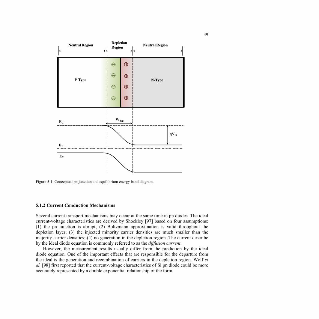
49
5.1.2 Current Conduction Mechanisms
Several current transport mechanisms may occur at the same time in pn diodes. The ideal current-voltage characteristics are derived by Shockley [97] based on four assumptions: (1) the pn junction is abrupt; (2) Boltzmann approximation is valid throughout the depletion layer; (3) the injected minority carrier densities are much smaller than the majority carrier densities; (4) no generation in the depletion region. The current describe by the ideal diode equation is commonly referred to as the diffusion current.
However, the measurement results usually differ from the prediction by the ideal diode equation. One of the important effects that are responsible for the departure from the ideal is the generation and recombination of carriers in the depletion region. Wolf et al. [98] first reported that the current-voltage characteristics of Si pn diode could be more accurately represented by a double exponential relationship of the form
Figure 5-1. Conceptual pn junction and equilibrium energy band diagram.
Neutral Region Neutral RegionDepletion Region
P-Type N-Type
EC
EF
EV
qVbi
Wdep

50
Jtotal = J0,diff expqVDn1kT
!
"#
$
%&'1
(
)*
+
,-+ J0,rec exp
qVDn2kT
!
"#
$
%&'1
(
)*
+
,-, (5.3)
where Jtotal is the total current density, J0,diff is the saturation current density for diffusion, J0,rec is the saturation current density for recombination in the depletion region, n1 and n2 are the ideality factors. n1 = 1 for the case of ideal diffusion current. The value of n2 depends on the location of the recombination centers within the bandgap. Typically, the expected n2 is close to 2.
Despite of the generation and recombination current in the depletion region, there are other non-ideal effects: (1) the surface effect; (2) the tunneling current via multiple defect sites; (3) the high-level injection effect (the injected minority carrier density is comparable to the majority carrier concentration); (4) the series resistance. The relative strength of the different current mechanisms depends on the properties of semiconductor materials, dopants, and the defects.
5.2 Temperature Sensing Mechanism
The diffusion current and the recombination current are the most important two current mechanisms in the temperature sensor based on 4H-SiC pn diode. At forward bias (qVF >> kT), a general form of the current density JF of the pn diode at a given applied bias-voltage VF can be then expressed using the following equation [94]-[96]:
JF = J0eqVFnkT , (5.4)
where q is the electric charge, k is Boltzmann constant, n is the ideality factor and has a value between 1 and 2.
When the diffusion current dominates, n = 1 and
J0 = qNCNVDN
LNNA
+DP
LPND
!
"#
$
%&e
'EgkT , (5.5)
where NC and NV are the effective density of conduction and valence band states, DN and DP are the diffusion coefficients of electrons and holes, LN and LP are the diffusion lengths of electrons and holes, ND and NA are the doping concentration in N-SiC and P-SiC, Eg is the bandgap energy.
When the recombination current dominates, n = 2 and
J0 =qniWdep
2! e, (5.6)
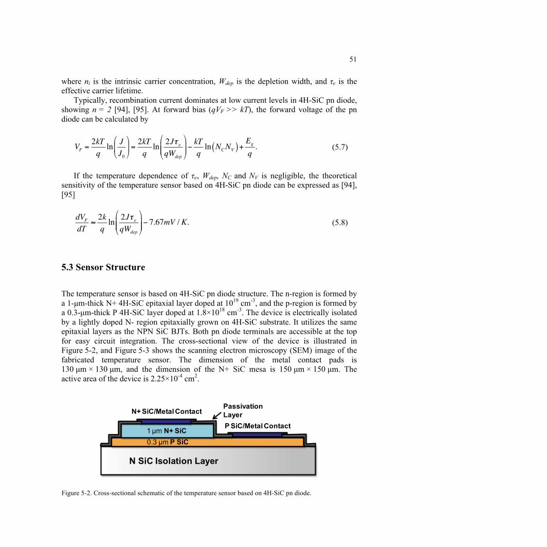
51
where ni is the intrinsic carrier concentration, Wdep is the depletion width, and τe is the effective carrier lifetime.
Typically, recombination current dominates at low current levels in 4H-SiC pn diode, showing n = 2 [94], [95]. At forward bias (qVF >> kT), the forward voltage of the pn diode can be calculated by
VF =2kTqln J
J0
!
"#
$
%&=2kTqln 2J! e
qWdep
!
"##
$
%&&'
kTqln NCNV( )+
Eg
q. (5.7)
If the temperature dependence of τe, Wdep, NC and NV is negligible, the theoretical
sensitivity of the temperature sensor based on 4H-SiC pn diode can be expressed as [94], [95]
dVFdT
!2kqln 2J! e
qWdep
"
#$$
%
&''( 7.67mV /K. (5.8)
5.3 Sensor Structure
The temperature sensor is based on 4H-SiC pn diode structure. The n-region is formed by a 1-µm-thick N+ 4H-SiC epitaxial layer doped at 1019 cm-3, and the p-region is formed by a 0.3-µm-thick P 4H-SiC layer doped at 1.8×1018 cm-3. The device is electrically isolated by a lightly doped N- region epitaxially grown on 4H-SiC substrate. It utilizes the same epitaxial layers as the NPN SiC BJTs. Both pn diode terminals are accessible at the top for easy circuit integration. The cross-sectional view of the device is illustrated in Figure 5-2, and Figure 5-3 shows the scanning electron microscopy (SEM) image of the fabricated temperature sensor. The dimension of the metal contact pads is 130 µm × 130 µm, and the dimension of the N+ SiC mesa is 150 µm × 150 µm. The active area of the device is 2.25×10⁻⁴ cm2.
Figure 5-2. Cross-sectional schematic of the temperature sensor based on 4H-SiC pn diode.
N SiC Isolation Layer
0.3 µm P SiC1 µm N+ SiC
PassivationLayerN+ SiC/Metal Contact
P SiC/Metal Contact
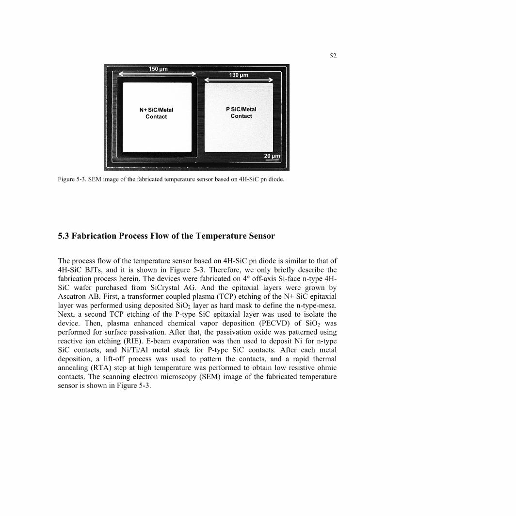
52
5.3 Fabrication Process Flow of the Temperature Sensor
The process flow of the temperature sensor based on 4H-SiC pn diode is similar to that of 4H-SiC BJTs, and it is shown in Figure 5-3. Therefore, we only briefly describe the fabrication process herein. The devices were fabricated on 4° off-axis Si-face n-type 4H-SiC wafer purchased from SiCrystal AG. And the epitaxial layers were grown by Ascatron AB. First, a transformer coupled plasma (TCP) etching of the N+ SiC epitaxial layer was performed using deposited SiO2 layer as hard mask to define the n-type-mesa. Next, a second TCP etching of the P-type SiC epitaxial layer was used to isolate the device. Then, plasma enhanced chemical vapor deposition (PECVD) of SiO2 was performed for surface passivation. After that, the passivation oxide was patterned using reactive ion etching (RIE). E-beam evaporation was then used to deposit Ni for n-type SiC contacts, and Ni/Ti/Al metal stack for P-type SiC contacts. After each metal deposition, a lift-off process was used to pattern the contacts, and a rapid thermal annealing (RTA) step at high temperature was performed to obtain low resistive ohmic contacts. The scanning electron microscopy (SEM) image of the fabricated temperature sensor is shown in Figure 5-3.
Figure 5-3. SEM image of the fabricated temperature sensor based on 4H-SiC pn diode.
20 µm
N+ SiC/Metal Contact
P SiC/Metal Contact
130 µm150 µm

53
5.4 Characterization Results
In this section, the characterization results of the fabricated temperature sensor based on 4H-SiC pn diode are going to be discussed. First, the current-voltage (I-V) characteristics at different temperatures are investigated. Then the device performance as a temperature sensor is evaluated.
5.4.1 I-V Measurements at Different Temperatures
The fabricated device was characterized at different temperatures. Figure 5-5 presents the I-V measurement results of the device from room temperature up to 600°C. The peak temperature was not limited by the device, but by the high temperature probe station. The figure shows that, by taking advantages of SiC material properties, stable device performance can be achieved at extremely high temperatures. From Figure 5-5, the ideality factor n of the fabricated device at low current levels was extracted to be 2.08 at room temperature and has a small variation of around 15% over the temperature range.
Figure 5-4. Cross-sectional process flow of the temperature sensor.
2. TCP etching of SiC to define N-type mesa
3. TCP etching of SiC to isolate the device
4. Oxide deposition for device passivation
5. Pattern oxide to open contact holes
6. 1st Metal deposition, patterning and annealing for N-SiC
7. 2nd Metal deposition, patterning and annealing for P-SiC
N-type SiC Isolation
N+ SiC Region
P SiC Region
MetalContact
SiO2
1. SiC carbide substrate with epi-layers

54
The extracted ideality factors and leakage currents at 20°C, 50°C and 100°C are indicated on the graph. For a given forward current level, the voltage decreases with increasing temperature.
5.4.2 Evaluation of the Temperature Sensor
Figure 5-6 illustrates the forward voltage versus temperature of the fabricated device at different forward current densities, respectively. The graph shows that the forward voltage of the device has a linear temperature dependence at all forward current levels, and it decreases with increasing temperature. By calculating the slopes of these linear relationships, temperature sensitivities can be obtained. At a forward current density of 0.44 A/cm2, a sensitivity of 2.3 mV/°C is achieved. At a lower current density of 0.44 mA/cm2, the sensitivity increases to 3.5 mV/°C. From Equation (5.8), it can be observed that the absolute value of dVF/dT, which is the sensitivity, is higher at lower current level.
Figure 5-7 shows the sensitivity versus forward current density relationship. A linear relationship is observed, and n = 2.0 can be extracted from the slope of the fitted curve showing that recombination current dominates the current flowing in the 4H-SiC pn diode in the measured current range. The results show a good agreement with the model described in Equation (5.8). Given the doping concentrations of the N+ and P regions, the corresponding depletion width is 0.047 µm. The carrier lifetime τe = 0.167 ns can also be
Figure 5-5. I-V measurement of the 4H-SiC pn diode based temperature sensor at different temperatures (20 – 600 °C).
n = 2.08I0 = 1.19 × 10⁻²⁴ mA
n = 2.11I0 = 1.19 × 10⁻²³ mA
n = 2.13I0 = 3.75 × 10⁻²² mA

55
Figure 5-7. Measured and modeled sensitivity vs. forward current density of the 4H-SiC pn diode temperature sensor. The extracted ideality factor and carrier lifetime are indicated on the graph.
Figure 5-6. Measured forward voltage vs. temperature at different forward current densities.
Measured SensitivityModeled Sensitivity
Extracted Ideality Factor n = 2.0Extracted Carrier Lifetime τe = 0.167 ns
Sensitivity = 3.5 mV/°C
Sensitivity = 2.3 mV/°C
56
extracted from the sensitivity versus forward current density relationship. The low carrier lifetime is mainly caused by the high density of interface traps at the SiO2/SiC interface.
In addition, the experimental results indicate that the proposed 4H-SiC pn diode achieves better sensitivities and higher operation temperatures in comparison with previously reported devices based on SiC Schottky diodes structures [91]-[93]. The sensitivity of the proposed device is also higher than the reported 4H-SiC pn diode betavoltaic cell [95] mainly due to the smaller depletion width and less impact of shunt resistance. The forward bias sensing mode can be used in the entire range from 20°C to 600°C and the forward voltage can be converted into a measurable variable by using a sensing circuit [91].
5.5 Conclusions
In this chapter, theoretical analysis and experimental results for a high-performance temperature sensor based on 4H-SiC pn diode are demonstrated. Thanks to the superior material properties of SiC, the temperature shows stable operation from room temperature up to 600 °C. Under forward bias condition, the temperature sensitivity of the sensor changes from 2.3 mV/°C at a forward current density of 0.44 A/cm2, to 3.5 mV/°C at a forward current density of 0.44 mA/cm2. Higher sensitivity can be achieved at a lower forward current level. The experimental results indicate a good agreement with the theoretical analysis. These results show that the device has the potential to be integrated with supporting circuitries to build a sensing module for high temperature applications.
57
Chapter 6 Conclusions and Future Research Directions
There are increasing interests on developing an integrated sensing module capable of operating at high temperatures. Such systems are beneficial to a number of industrial applications. A high temperature integrated circuit is an important part of such systems, because it can provide power management function for the energy scavenger, build the electrical interface with MEMS-based harsh environment sensors, and amplify the sensing signals. Therefore, it is essential to have transistors, the building blocks of integrated circuits, which can operate at high temperatures. This dissertation presents potential solutions for the above problems. This chapter concludes the research efforts on developing 4H-SiC BJTs, which are capable of operating at extremely high temperatures. A high temperature sensor based on 4H-SiC pn diode is also demonstrated. Finally, suggestions on possible future research directions are made.
6.1 Summary
The main outcomes of this work are 1) the study of physical models for describing the electrical behaviors of SiC devices, 2) the development of fabrication process for SiC based electrical devices, 3) the design and development of 4H-SiC NPN BJTs that are capable of stable operation up to 400 °C, 4) the design and development of temperature sensor based on 4H-SiC pn diode which shows stable operation in a temperature range from 20 °C to 600 °C, 5) the device characterization at room temperature and at elevated temperatures.
Physical models are studied to describe the device behaviors. Especially, the temperature dependences of material electrical properties are essential to understand the device performance at elevated temperatures. Numerical device simulators are used to design the devices and investigate the device behaviors. Appropriate physical models with proper material properties are necessary to obtain accurate simulation results. Physical models of band structure, mobility, incomplete ionization and generation-
58
recombination are discussed. Special emphasis goes to the temperature dependence of carrier concentration and carrier lifetime. The understanding of the current device will work as guidelines for optimization of the device performance in the future.
Fabrication process for SiC based electrical devices was developed. Though some of the Si processing technologies can be applied to SiC, there are still differences from standard Si process due to the chemical inertness and the thermal stability of SiC. For the etching process, there is no known chemical that can wet etch single crystal SiC at room temperature. TCP/ICP etching is commonly used instead. To avoid the trenching effect, which usually happens during the plasma etching process, HBr and Cl2 based etching chemistry was studied. Good sidewall profile and high selectivity were obtained by using the optimized recipe. Metallization process is also important for getting good devices. The quality of ohmic contacts could affect the operation and performance of the devices. Different metal layers and metal stacks are tested, with various high temperature annealing conditions. Ni was chosen for n-type SiC contacts, and optimized annealing condition is 2 minutes at 1000 °C. The contact resistance and specific contact resistance are 5.14 Ω and 1.37×10⁻⁴ Ωcm2 respectively. For the p-type SiC contacts, Ni/Ti/Al metal stack is utilized. After annealing the contact at 800 °C for 1 minutes, the contact resistance and specific contact resistance are 664 Ω and 2.18×10⁻³ Ωcm2 respectively. Some issues with the surface passivation method were addressed and discussed. Due to the remaining carbon cluster at the SiO2/SiC interface during the oxidation process, serious degradation of the dielectric layer quality is observed. Nitridation of the oxide has been shown to be an effective way to improve the quality of the interface. The device performance could be improved if this process can be applied in the future.
4H-SiC NPN BJTs were designed for high temperature sensing applications that usually require low voltage, analog integrated circuits. The thickness and doping concentration of the epitaxial layers were designed to have high current gain β and high output resistance ro. The proposed device was fabricated and comprehensively characterized at room temperature and at elevated temperatures. The device showed stable operation up to 400 °C. At high temperatures, although the current gain of the device is reduced, the output resistance increases. The intrinsic voltage gain of 5900 is achieved at 400 °C, which is higher than 3300 at room temperature. The results show that 4H-SiC BJT has the potential to be used as a voltage amplifier at extremely high temperatures.
Finally, a high-performance temperature sensor based on 4H-SiC pn diode is demonstrated. The device showed stable operation from room temperature up to 600 °C. The operating mechanism of the temperature sensor was discussed based on pn junction diode physics. In forward biased region, the forward voltage of the 4H-SiC pn diode shows linear dependence on temperature at a constant current. This dependence is utilized to sense temperature variations and the proposed device achieves a high sensitivity of 3.5 mV/°C. This type of temperature sensor has the advantages of high sensitivity and compatibility with integrated circuits. The successful demonstration of the temperature sensor based on 4H-SiC pn diode opens the possibility to the integration with supporting circuitries to build a sensing module that is capable of working at extremely high temperatures.
59
6.2 Future Research Directions
Future work for this project is needed for the optimization of the device performance, and for the development of complementary circuit elements for high performance ICs that can reliably operate at extremely high temperatures. • Improvement of fabrication process
The surface passivation process needs to be improved to reduce the interface trap density. The quality of the interface between SiC and the surface passivation layer has a strong effect on the current gain of SiC BJTs. High temperature annealing of thermally grown or deposited SiO2 in NO or N2O should be studied. Substituting SiO2 with other dielectric, such as AlN or aluminum oxide (Al2O3), could also be investigated.
Metallization process also needs further investigation. In this work, Ni is used for N-type SiC contacts and Ni/Ti/Al metal stack is used for P-type SiC contacts. Though both contacts showed stable operation up to 600 °C, long-term stability test should be performed to study the electrical behaviors of the contacts. To further extend the operating temperature of the device, more metals need to be explored, especially for P-type SiC contacts. TiW is a strong candidate since it is very stable at high temperatures and can work for both N-type and P-type SiC.
• Development of high performance 4H-SiC NPN BJTs
A further analysis on the influences of design parameters, such as geometry parameters, doping concentrations and thicknesses of the epitaxial layers, should be developed for achieving better current gain and output resistance. To further increase the current gain, poly-SiC emitter instead of all-crystalline emitter could be used. Poly-emitter structure can improved the emitter injection efficiency, and thus is widely used in Si BJTs to improve the current gain. TCAD simulation results show that a 15% increase of the maximum current gain can be obtained by using a poly-emitter SiC BJT.
• Development of complementary circuit elements By carefully designing the epitaxial layers, complementary circuit elements, such as PNP BJTs, can be fabricated together with NPN BJTs in the same fabrication run. In addition, other types of transistors can be fabricated as well with minimum additional process steps. JFETs have the advantage of high input impedance, which is a desirable feature for sensing circuitry. However, they are normally-on devices with low transconductance and high forward voltage drop, which make them less appealing. By redesigning the epitaxial layers, it is possible to have JFETs fabricated together with NPN BJTs. The capability of having multiple types of transistors on the same chip gives circuit designers more flexibility.
60
Bibliography
1. C.-M. Zetterling, Process technology for silicon carbide devices, London: IEE, 2002.
2. K. Hamada, “Present Status and Future Prospects for Electronics in EVs/HEVs and Expectations for Wide Bandgap Semiconductor Devices,” Materials Science Forum, vol. 600- 603, pp. 889-893, 2009.
3. Toyota Motor Sales, USA Inc. Emissions #1 - Combustion Chemistry. http://www.autoshop101.com/forms/h55.pdf.
4. M. Yoon, K. Lee, M. Sunwoo, “A Method for Combustion Phasing Control Using Cylinder Pressure Measurement in a CRDI Diesel Engine,” Mechatronics, vol. 17, pp. 469-479, 2007.
5. G. H. Koretz, M. H. Eickhoff, H. Moeller, “Silicon Compatible Materials for Harsh Environment Sensors,” Sensors and Actuators, vol. 74, pp. 182-189, 1999.
6. G. A. Baum, “Manufacturing Process Control for Industry of the Future,” National Academy Press, Washington, D.C. Publication NMAB-487-2, 1998.
7. K. C. Schadow, “MEMS Aerospace Applications,” NATO Research and Technology Organization, RTO-EN-AVT-105, 2004.
8. C. R. Farrar, K. Worden. “An Introduction to Structural Health Monitoring,” Philosophical Transactions of Royal Society A, vol. 365, pp. 303-315, 2007.
9. M. B. J. Wijesundara and R.G. Azevedo, Silicon Carbide Microsystems for Harsh Environments, New York: Springer, 2011.
10. P. G. Neudeck, R. S. Okojie, and L.-Y. Chen, “High-temperature electronics - a role for wide bandgap semiconductors,” Proceedings of IEEE, vol. 90, pp. 1065-1076, Jun. 2002.
11. D. G. Senesky, B. Jamshidi, K. B. Cheng, and A. P. Pisano, “Harsh environment silicon carbide sensors for health and performance monitoring of aerospace systems: a review,” IEEE Sensors Journal, vol. 9, pp. 1472-1478, Nov. 2009.
12. X. Gong, L. An, and C. Xu, “Wireless passive sensor development for harsh environment applications,” 2012 IEEE International Workshop on Antenna Technology (iWAT), pp. 140-143, Mar. 2012.
13. H.-S. Lee, Fabrication and Characterization of Silicon Carbide Power Bipolar Junction Transistors, Doctorial Thesis, Department of Microelectronics and Applied Physics (MAP), KTH, Royal Institute of Technology, Stockholm, Sweden, 2008.
61
14. K. H. J. Bushchow, R. W. Cahn, M. C. Flemings, B. Ilschner, E. J. Kramer, S. Mahajan, and P. Veyssiere Eds., Encyclopedia of Materials: Science and Technology, New York: Elsevier, 2001.
15. H. Miyake, Interface Control of AlGaN/SiC Heterojunction and Development of High-Current-Gain SiC-Based Bipolar Transistors, Ph.D. dissertation, Electronic Science and Engineering, Kyoto University, Japan, 2012.
16. D. M. Brown, M. Ghezzo, J. Kretchmer, V. Krishnamurthy, G. Michon, and G. Gati, “High temperature silicon carbide planar IC technology and first monolithic SiC operational amplifier IC,” In Transaction 2nd International High Temperature Electronics Conference, Charlotte NC, p. XI, 1994.
17. D. M. Brown, E. Downey, M. Ghezzo, J. Kretchmer, V. Krishnamurthy, W. Hennessy, and G. Michon, “Silicon Carbide MOSFET Integrated Circuit Technology,” Physica status solidi (a), vol. 162, pp. 459-479, 1997.
18. D. T. Clark, E. P. Ramsay, A. E. Murphy, D. A. Smith, R. F. Thompson, R. A. R.Young, J. D. Cormack, C. Zhu, S. Finney, and J. Fletcher, “High temperature silicon carbide CMOS integrated circuits,” Materials Science Forum, vol. 679-680, pp.726-729, 2011.
19. D. J. Spry, P. G. Neudeck, L.-Y. Chen, G. M. Beheim, R. S. Okojie, C. W. Chang, R. D. Meredith, T. L. Ferrier, and L. J. Evans, “Fabrication and testing of 6H-SiC JFETs for prolonged 500 °C operation in air ambient,” Materials Science Forum, vol. 600-603, pp.1079-1082, 2009.
20. P. G. Neudeck, D. J. Spry, L.-Y. Chen, G. M. Beheim, R. S. Okojie, C. W. Chang, R. D. Meredith, T. L. Ferrier, L. J. Evans, M. J. Krasowski, and N. F. Prokop, “Stable electrical operation of 6H-SiC JFETs and ICs for thousands of hours at 500 °C,” IEEE Electron Device Letters, vol. 29, pp. 456-459, 2008.
21. P. G. Neudeck, L.-Y. Chen, M. J. Krasowski, and N. F. Prokop, “Characterization of 6H-SiC JFET integrated circuits over a broad temperature range from -150 °C to +500 °C,” Materials Science Forum, vol. 645-648, pp. 1135-1138, 2010.
22. A. C. Patil, F. Xiao-An, M. Mehregany, and S. L. Garverick, “Fully-monolithic, 600 °C differential amplifiers in 6H-SiC JFET IC technology,” Custom Integrated Circuits Conference, IEEE, pp. 73-76, 2009.
23. C.-W. Soong, A. C. Patil, S. L. Garverick, F. Xiaoan Fu, and M. Mehregany, “550 °C integrated logic circuits using 6H-SiC JFETs,” Electron Device Letters, IEEE, vol. 33, pp. 1369-1371, 2012.
24. P. G. Neudeck, D. J. Spry, L.-Y. Chen, R. S. Okojie, G. M. Beheim, R. Meredith, and T. Ferrier, “SiC field effect transistor technology demonstrating prolonged stable operation at 500 °C,” Materials Science Forum, vol. 556-557, pp. 831-834, 2007.

62
25. S.-H. Ryu, A. K. Agarwal, R. Singh, and J. W. Palmour, “1800 V NPN bipolar junction transistors in 4H-SiC,” IEEE Electron Device Letters, vol. 22, pp.124-126, 2001.
26. C.-F. Huang, and J. A. Cooper, Jr., “High current gain 4H-SiC npn bipolar junction transistors,” IEEE Electron Device Letters, vol. 24, pp. 396-398, 2003.
27. J. Zhang, Y. Luo, P. Alexandrov, L. Fursin, J. H. Zhao, “A high current gain 4H-SiC NPN power bipolar junction transistor,” IEEE Electron Device Letters, vol. 24, pp. 327-329, 2003.
28. J. Zhang, X. Li, P. Alexandrov, L. Fursin, X. Wang, J. H. Zhao, “Fabrication and characterization of high-current-gain 4H-SiC bipolar junction transistors,” IEEE Transactions on Electron Devices, vol. 55, pp. 1899-1906, 2008.
29. H.-S. Lee, M. Domeij, C.-M. Zetterling, M. Ostling, F. Allerstam, and E. O. Sveinbjornsson, “1200-V 5.2-mΩ·cm2 4H-SiC BJTs with a high common-emitter current gain,” IEEE Electron Device Letters, vol. 28, pp. 1007-1009, 2007.
30. R. Ghandi, H.-S. Lee, M. Domeij, B. Buono, C.-M. Zetterling, and M. Ostling, “Fabrication of 2700-V 12 mΩ·cm2 non ion-implanted 4H-SiC BJTs with common-emitter current gain of 50,” IEEE Electron Device Letters, vol.29, pp. 1135-1137, 2008.
31. S. Singh, and J. A. Cooper, “Bipolar integrated circuits in 4H-SiC,” IEEE Transactions on Electron Devices, vol. 58, pp. 1084-1090, 2011.
32. S. Singh, High-performance TTL bipolar integrated circuits in 4H-SiC, Ph.D. dissertation, Purdue University, USA, 2010.
33. N. Zhang, Y. Rao, N. Xu, A. Maralani, and A. P. Pisano, “Characterization of 4H-SiC bipolar junction transistor at high temperatures,” Material Science Forum, vol. 778-780, pp. 1013-1016, 2014.
34. R. F. Pierret, Semiconductor Device Fundamentals, New York: Wiley, 1996. 35. D. A. Neamen, Semiconductor Physics and Devices: Basic Principles, 3rd Edition,
New York: McGraw-Hill, 2003. 36. M. E. Levinshtein, S. L. Rumyantsev, and M. S. Shur, Ed., Properties of Advanced
Semiconductor Materials: GaN, AlN, InN, BN, SiC, SiGe, New York: Wiley, 2001. 37. D. A. Neamen, An Introduction to Semiconductor Devices, New York: McGraw-Hill,
2006, pp. 501-502. 38. U. Lindefelt, “Doping-induced band edge displacements and band gap narrowing in
3C-, 4H-, 6H-SiC and Si,” Journal of Applied Physics, vol. 84, pp. 2628–2637, Sept. 1998.
39. D. M. Caughey and R. E. Thomas, “Carrier mobilities in silicon empirically related to doping and field,” Proceedings of the IEEE, vol. 55, pp. 2192–2193, Dec. 1967.

63
40. W. J. Schaffer, G. H. Negley, K. G. Irvine and J. W. Palmour, “Conductivity anisotropy in eptaxial 6H and 4H SiC,” MRS Proceedings, vol. 339, pp. 595–600, 1994.
41. X. Li, Y. Luo, L. Fursin, J. H. Zhao, M. Pan, P. Alexandrov, and M. Weiner, “On the temperature coefficient of 4H-SiC BJT current gain,” Solid-State Electronics, vol. 47, pp. 233-239, Feb. 2003.
42. G. L. Harris, Ed., Properties of Silicon Carbide, London: INSPEC, The Insititution of Electrical Engineers, 1995, pp. 87-91.
43. W. Götz, A. Schöner, and G. Pensl, “Nitrogen donors in 4H-silicon carbide,” Jounal of Applied Physics, vol. 73, pp. 3332-3338, Apr. 1993.
44. M. Bakowski, and U. Gustafsson, and U. Lindefelt, “Simulation of SiC high power devices,” Physica Status Solidi (A), vol. 162, pp. 421-440, Jul. 1997.
45. M. Ikeda, H. Matsunami, and T. Tanaka, “Site effect on the impurity levels in 4H, 6H, and 15R SiC,” Physical Review B, vol. 22, pp. 2842-2854, Sept. 1980.
46. R. S. Muller and T. I. Kamins, Device Electronics for Integrated Circuits, 3rd Edition, New York: Wiley, 2003.
47. W. Shockley and W. T. Read, “Statistics of the recombinations of the holes and electrons,” Physical Review, vol. 87, pp. 835 - 842, Sept. 1952.
48. R. N. Hall, “Electron-hole recombination in germanium,” Physical Review, vol. 87, pp. 387, Jul. 1952.
49. M. Ruff, H. Mitlehner, and R. Helbig “SiC devices: physics and numerical simulation,” IEEE Transactions on Electron Devices, vol. 41, pp. 1040-1054, Jun. 1994.
50. O. Kordina and J. P. Bergman, “The minority carrier lifetime of n-type 4H- and 6H-SiC epitaxial layers,” Applied Physics Letters, vol. 69, pp. 679-681, Jul. 1996.
51. A. G. Acheson, England Patent 17911, 1892. 52. J. A. Lely, “Darstellung von Einkristallen von Silicium carbid und Beherrschung
von Art und Menge der eingebautem Verunreingungen,” Berichte der Deutschen Keramischen Gesellschaft, vol. 32, pp. 229, 1955.
53. Y. M. Tairov, and V. F. Tsvetkov, “Investigation of growth processes of ingots of silicon carbide single crystals,” Journal of Crystal Growth, vol. 43, pp. 209, 1978.
54. Y. M. Tairov, and V. F. Tsvetkov, “General principles of growing large-size single crystals of various silicon carbide polytypes,” Journal of Crystal Growth, vol. 52, pp. 146, 1981.
55. G. Brauer, W.Anwand, W. Skorupa, S. Brandstetter, C. Teichert, “Characterization of 6H-SiC surfaces after ion implantation and annealing using positron annihilation spectroscopy and atomic force microscopy,” Journal of Applied Physics, vol. 99, pp. 023523, 2006.

64
56. L. Ruppalt, S. Stafford, D. Yuan, R. Vispute, T. Venkatesan, R. Sharma, K. Jones, M. Ervin, K. Kirchner, T. Zheleva, M. Wood, B. Geil, E. W. Forsythe, “Using a PLD BN/AlN composite as an annealing cap for ion implanted SiC,” 2001 International Semiconductor Device Research Symposium, pp. 529-530, 2001.
57. P. H. Yih, V. Saxena, and A. J. Steckl, “A review of SiC reactive ion etching in fluorinated plasmas,” Physica Status Solidi (B), vol. 202, pp. 605-642, 1997.
58. S. Tanaka, K. Rajanna, T. Abe, and M. Esashi, “Deep reactive ion etching of silicon carbide,” Journal of Vacuum Science & Technology B, vol. 19, pp. 2173-2176, 2001.
59. F. A. Khan and I. Adesida, “High rate etching of SiC using inductive coupled plasma reactive ion etching in SF6-based gas mixtures,” Applied Physics Letters, vol. 75, pp. 2268, 1999.
60. N. O. V. Plank, M. A. Blauw, E. W. J. M. van der Drift and R. Cheung, “The etching of silicon carbide in inductively coupled SF6/O2 plasma,” Journal of Physics D: Applied Physics, vol. 36 pp.482-487, 2003.
61. D. Gao, R. T. Howe, and R. Maboudian, “High-selectivity etching of polycrystalline 3C-SiC films using HBr-based transformer coupled plasma,” Applied Physics Letters, vol. 82, pp. 1742, 2003.
62. D. Gao, M. B. J. Wijesundara, C. Carraro, R. T. Howe, and R. Maboudian, “Recent progress toward a manufacturable polycrystalline SiC surface micromachining technology,” IEEE Sensors Journal, vol. 4, pp. 441-448, 2004.
63. Electronic Materials Research Laboratory, <http://www.emrl.de/r_m_6.html>.
64. N. Lundberg and M. Östling, “CoSi2 ohmic contacts to n-type 6H-SiC,” Solid-State Electronics, vol. 38, pp. 2023-2028, 1995.
65. R. S. Okojie, D. Lukco, Y. L. Chen, and D. J. Spry, “Reliability assessment of Ti/TaSi2/Pt ohmic contacts on SiC after 1000 h at 600 °C,” Journal of Applied Physics, vol. 91, pp. 6553-6559, 2002.
66. H.-S. Lee, M. Domeij, C.-M. Zetterling, M. Östling and J. Lu, “Investigation of TiW contacts to 4H-SiC bipolar junction devices,” Material Science Forum, vol. 527-529, pp. 887-890, 2006.
67. S. Tanimoto, N. Kiritani, M. Hoshi, and H. Okushi, “Ohmic contact structure and fabrication process applicable to practical SiC devices,” Material Science Forum, vol.389-393, pp. 879-884, 2001.
68. S.-K. Lee, C.-M. Zetterling, M. Östling, J.-P. Palmquist, H. Hoberg, and U. Jansson, “Low resistivity ohmic titanium carbide contacts to n- and p-type 4H-silicon carbide,” Solid-State Electronics, vol. 44, pp. 1179-1186, 2000.
69. L. G. Fursin, J. H. Zhao, and M. Weiner, “Nickel ohmic contacts to p and n-type 4H-SiC,” Electronics Letters, vol. 37, pp. 1092, 2001.
70. N. A. Papanicolaou, A. Edwards, M. V. Rao, and W. T. Anderson, “Si/Pt Ohmic contacts to p-type 4H-SiC,” Applied Physics Letters, vol. 73, pp. 2009, 1998.

65
71. Lin, J.Y., Mohney, S.E., Smalley, M., Crofton, J., Williams, J.R., and Isaacs-Smith, T., “Engineering the Al-Ti/p-SiC ohmic contact for improved performance,” Materials Research Society Symposium Proceedings, vol. 640, pp. H7.3.1, 2001.
72. D. K. Schroder, Semiconductor Material and Device Characterization, 3rd Edition, New York: Wiley, 2006.
73. Y. Song, S. Dhar, and L. C. Feldman, “Modified Deal Grove model for the thermal oxidation of silicon carbide,” Journal of Applied Physics, vol. 75, pp. 4953, 2004.
74. V. V. Afanasev, M. Bassler, G. Pensl, and M. Schulz, “Intrinsic SiC/SiO2 interface states,” Physica Status Solidi (A), vol. 162, pp. 321-337, 1997.
75. R. Schömer, P. Friedrichs, D. Peters, and D. Stephani, “Significantly improved performance of MOSFETs on silicon carbide using the 15R-SiC polytype,” IEEE Electron Device Letters, vol. 20, pp. 241-244, 1999.
76. N. S. Saks, S. S. Mani, and A. K. Agarwal, “Interface trap profile near the band edges at the 4H-SiC/SiO2 interface,” Applied Physics Letters, vol. 76, pp. 2250, 2000.
77. R. Ghandi, B. Buono, M. Domeij, R. Esteve. A. Schöner, J. Han, S. Dimitrijev, S. A. Reshanov, C.-M. Zetterling, M. Östling, “Surface-passivation effects on the performance of 4H-SiC BJTs,” IEEE Transactions on Electron Devices, vol. 58, pp. 259-265, 2011.
78. R. Schömer, P. Friedrichs, D. Peters, D. Stephani, S. Dimitrijev, and P. Jamet, “Enhanced channel mobility of 4H-SiC metal-oxide-semiconductor transistors fabricated with standard polycrystalline silicon technology and gate-oxide nitridation” Applied Physics Letters, vol. 80, pp. 4253, 2002.
79. H.-S. Lee, M. Domeij, C.-M. Zetterling, M. Östling, F. Allerstam, and E. Ö. Sveinbjörnesson, “Surface passivation oxide effects on the current gain of 4H-SiC bipolar junction transistors,” Applied Physics Letters, vol. 92, pp. 082113, 2008.
80. H.-S. Lee, M. Domeij, C.-M. Zetterling, M. Östling, F. Allerstam, and E. Ö. Sveinbjörnesson, “1200-V 5.2-mΩ·cm2 4H-SiC BJTs With a High Common-Emitter Current Gain,” IEEE Electron Device Letters, vol. 28, pp. 1007-1009, 2007.
81. G. Y. Chung, C. C. Tin, J. R. Williams, K. McDonald, R. K. Chanana, R. A. Weller, S. T. Pantelides, L. C. Feldman, O. W. Holland, and M. K. Das, and J. W. Palmour, “Improved inversion channel mobility for 4H-SiC MOSFETs following high temperature anneals in nitric oxide,” IEEE Electron Device Letters, vol. 22, pp. 176-178, 2001.
82. S. Dhar, Y. W. Song, L. C. Feldman, T. Isaacs-Smith, C. C. Tin, J. R. Williams, G. Chung, T. Nishimura, D. Starodub, T. Gustafsson, and E. Garfunkel, “Effect of nitric oxide annealing on the interface trap density near the conduction bandedge of 4H-SiC at the oxide/(1120) 4H-SiC interface,” Applied Physics Letters, vol. 84, pp. 1498, 2004.

66
83. K. Fujihira, Y. Tarui, K. Ohtsuka, M. Imaizumi, and T. Takami, “Effect of N2O anneal on channel mobility of 4H-SiC MOSFET and gate oxide reliability,” Materials Science Forum, vol. 483-485, pp. 697-700, 2005.
84. T. Kimoto, Y. Kanzaki, M. Noborio, H. Kawano, and H. Matsunami, “Interface properties of metal-oxide-semiconductor structures on 4H-SiC (0001) and (1120) formed by N2O oxidation,” Japanese Journal of Applied Physics, vol. 44, pp. 1213-1218, 2005.
85. Y. Nanen, M. Kato, J. Suda, and T. Kimoto, “Effects of nitridation on 4H-SiC MOSFETs fabricated on various crystal faces,” IEEE Transactions on Electron Devices, vol. 60, pp.1260-1262, 2013.
86. T. Kimoto, H. Kawano, M. Noborio, J. Suda, and H. Matsunami, “Improved dielectric and interface properties of 4H-SiC MOS structures processed by oxide deposition and N2O annealing,” Materials Science Forum, vol. 527-529, pp. 987-990, 2006.
87. H. Miyake, T. Kimoto, and J. Suda, “Improvement of current gain in 4H-SiC BJTs by surface passivation with deposited oxides nitrided in N2O or NO,” IEEE Electron Device Letters, vol. 32, pp. 285-287, 2011.
88. P. Jamet, S. Dimitrijev, and P. Tanner, “Effects of nitridation in gate oxides grown on 4H-SiC,” Journal of Applied Physics, vol. 90, pp. 5058, 2001.
89. S. Potbhare, N. Goldsman, G. Pennington, A. Lelis, and J. M. McGarrity, “Numerical and experimental characterization of 4H-silicon carbide lateral metal-oxide-semiconductor field-effect transistor,” Journal of Applied Physics, vol. 100, pp. 044515, 2006.
90. S. Potbhare, N. Goldsman, G. Pennington, J. M. McGarrity, and A. Lelis, “Characterization of 4H-SiC MOSFET Interface Trap Charge Density Using a First Principles Coulomb Scattering Mobility Model and Device Simulation,” 2005 International Conference on Simulation of Semiconductor Processes and Devices, pp. 95-98, 2005.
91. F. Draghici, M. Badila, G. Brezeanu, I. Rusu, F. Craciunoiu, I. Enache, “An industrial temperature probe based on SiC diodes,” 2010 International Semiconductor Conference (CAS), vol. 2, pp. 409-412, 2010.
92. I. Josan, C. Boianceanu, G. Brezeanu, V. Obreja, M. Avram, D. Puscasu, A. Ioncea, “Extreme environment temperature sensor based on silicon carbide Schottky diode,” 2009 International Semiconductor Conference (CAS), vol. 2, pp. 525-528, 2009.
93. R. Pascu, F. Draghici, M. Badila, F. Craciunoiu, G. Brezeanu, A. Dinescu, I. Rusu, “High temperature sensor based on SiC Schottky diodes with undoped oxide ramp termination,” 2011 International Semiconductor Conference (CAS), vol. 2, pp. 379-382, 2011.
67
94. N. Zhang, C. -M. Lin, D. G. Senesky, and A. P. Pisano, “Temperature sensor based on 4H-silicon carbide pn diode operational from 25°C to 600°C,” Applied Physics Letters, vol. 104, 073504, Feb. 2014.
95. M. V. S. Chandrashekhar, R. Duggirala, M. G. Spencer, and A. Lal, “4H SiC betavoltaic powered temperature transducer,” Applied Physics Letters, vol. 91, 053511, Aug. 2007.
96. S. M. Sze, Physics of Semiconductor Devices, 2nd Edition, New York: Wiley, 1981.
97. W. Shockley, “The theory of p-n junctions in semiconductors and p-n junction transistors,” Bell System Technical Journal, vol. 28, pp. 435-489, Jul. 1949.
98. M. Wolf, G. T. Noel, and R. J. Stirn, “Investigation of the double exponential in the current-voltage characteristics of silicon solar cells,” IEEE Transactions on Electron Devices, vol. 24, pp. 419-428, Apr. 1977.