signal conditioning circuits :power supplies
TRANSCRIPT
คณะวศวกรรมศาสตรมหาวทยลยธรรมศาสตร
Measurement and Instrumentation
Signal Conditioning Circuits
:Power Supplies

Electronic measurement system
Transducer
Conditioning
circuits
Amplifier
Recorder
Data
processor
Controller
Power
supply
Command
generator
For engineering analysis
- Graphs or Tables
Process control
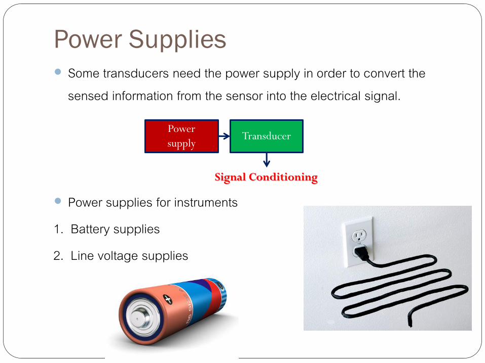
Power Supplies Some transducers need the power supply in order to convert the
sensed information from the sensor into the electrical signal.
Power supplies for instruments1. Battery supplies2. Line voltage supplies
TransducerPower
supply
Signal Conditioning
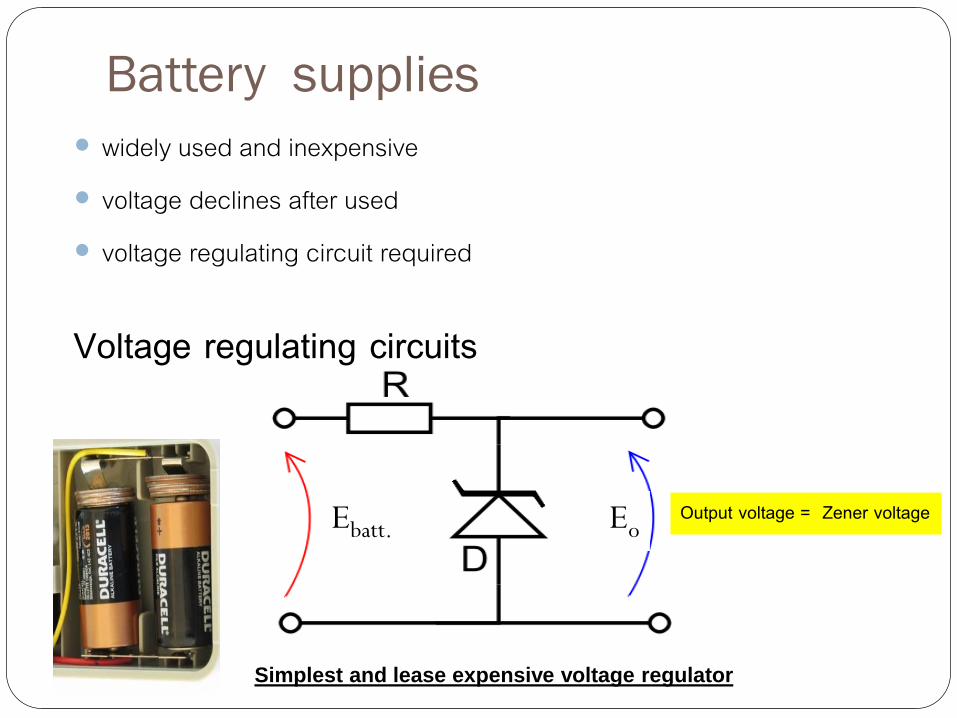
Battery supplies
widely used and inexpensive voltage declines after used voltage regulating circuit required
Voltage regulating circuits
Output voltage = Zener voltageEbatt. Eo
Simplest and lease expensive voltage regulator
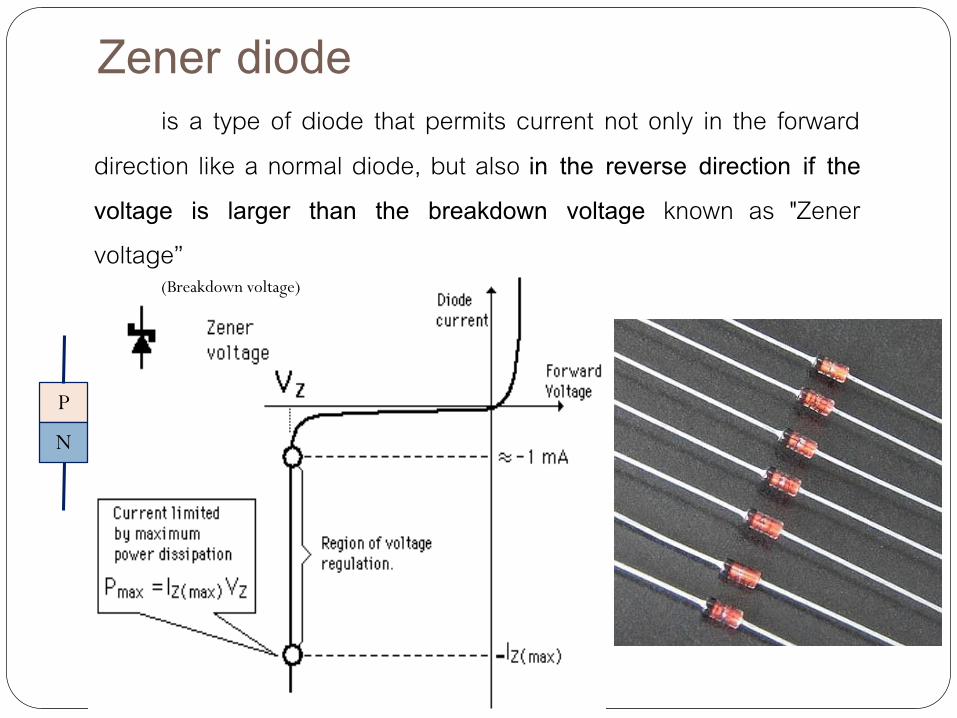
Zener diodeis a type of diode that permits current not only in the forward
direction like a normal diode, but also in the reverse direction if the voltage is larger than the breakdown voltage known as "Zener voltage”
(Breakdown voltage)
P
N
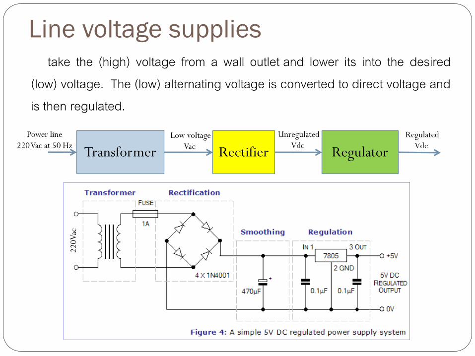
Line voltage suppliestake the (high) voltage from a wall outlet and lower its into the desired
(low) voltage. The (low) alternating voltage is converted to direct voltage and is then regulated.
RectifierTransformer Regulator
Power line
220 Vac at 50 HzLow voltage
Vac
Unregulated
Vdc Regulated
Vdc
220V
ac
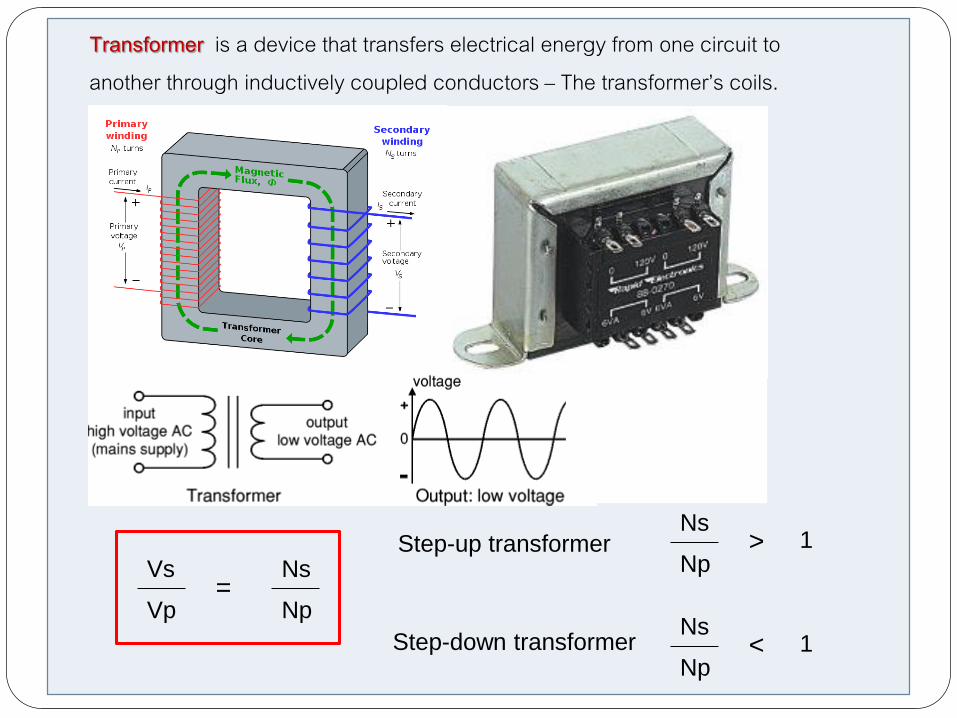
Transformer is a device that transfers electrical energy from one circuit to another through inductively coupled conductors – The transformer’s coils.
Vs
Vp
Ns
Np=
Step-up transformer
Step-down transformer
Ns
Np1>
Ns
Np1<

Rectifier is an electrical device that converts alternating current (AC), which periodically reverses direction, to direct current (DC), which is in only one direction
Vdc = Vav = 2Vp/p
Vrms = Vp/2

Voltage regulator is an electrical regulator designed to automatically maintain a constant voltage level
Three pin 12 V DC voltage regulator IC.
คณะวศวกรรมศาสตรมหาวทยลยธรรมศาสตร
Measurement and Instrumentation
Signal Conditioning Circuits
:Bridge Circuits

Bridge circuits
have been devised for measuring capacitance, inductance, and
most often for measuring resistance. A purely
resistance bridge, called a “Wheatstone bridge”, provides a
means for accurately measuring resistance, and for detecting
small changes in resistance.
Galvanometer
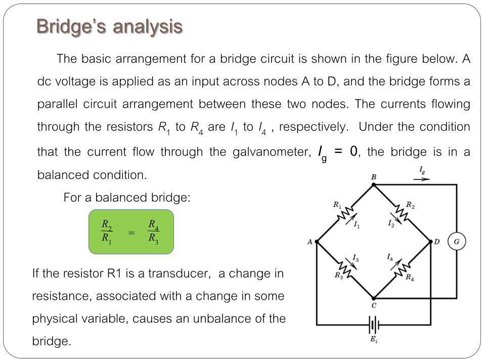
Bridge’s analysisThe basic arrangement for a bridge circuit is shown in the figure below. A
dc voltage is applied as an input across nodes A to D, and the bridge forms aparallel circuit arrangement between these two nodes. The currents flowingthrough the resistors R1 to R4 are I1 to I4 , respectively. Under the conditionthat the current flow through the galvanometer, Ig = 0, the bridge is in abalanced condition.
For a balanced bridge:
If the resistor R1 is a transducer, a change inresistance, associated with a change in somephysical variable, causes an unbalance of thebridge.
R2 R4R1 R3
=
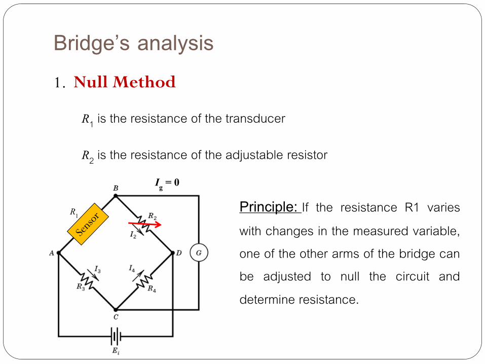
1. Null Method
Bridge’s analysis
R1 is the resistance of the transducer
R2 is the resistance of the adjustable resistor
R1Principle: If the resistance R1 varies with changes in the measured variable, one of the other arms of the bridge can be adjusted to null the circuit and determine resistance.
Ig = 0
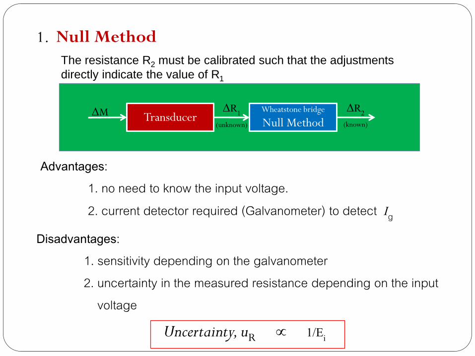
1. Null Method
TransducerWheatstone bridge
Null MethodDM DR1 DR2
(unknown) (known)
Advantages: 1. no need to know the input voltage.2. current detector required (Galvanometer) to detect Ig
Disadvantages: 1. sensitivity depending on the galvanometer2. uncertainty in the measured resistance depending on the input
voltage
Uncertainty, uR 1/Ei
The resistance R2 must be calibrated such that the adjustments
directly indicate the value of R1

2. Deflection Method
Bridge’s analysis
R1 is the resistance of a transducer
R1
Principle: a voltage measuring device is used to measure the voltage unbalance in the bridge (the voltage drop from B to C) as a n indication of the change in resistance.
𝐸𝑜 = 𝐸𝑖 𝑅1
𝑅1 + 𝑅2−
𝑅3
𝑅3 + 𝑅4
2. Deflection Method
R1R1 = R2 = R3 = R4 = R
TransducerWheatstone bridge
Deflection MethodDM d R d Eo
𝛿𝐸𝑜
𝐸𝑖 =
𝛿𝑅/𝑅
4 + 2(𝛿𝑅/𝑅)
EEo
For identical resistors,
Under balanced conditions (Ig = 0),
In an unbalanced condition,
Eo = 0

Advantage: can be used to measure time-varying signals, but the voltage measuring device must have the frequency response not less than that of the sensor.
Disadvantage: 1. high capability of the galvanometer required.2. known and regulated input voltage required.
In case of the low impedance galvanometer, Rg
𝐼𝑔 = 𝐸𝑖
𝛿𝑅/𝑅
4(𝑅 + 𝑅𝑔)
𝐸𝑜 = 𝐸𝑖
𝛿𝑅/𝑅
4(1 + 𝑅/𝑅𝑔)
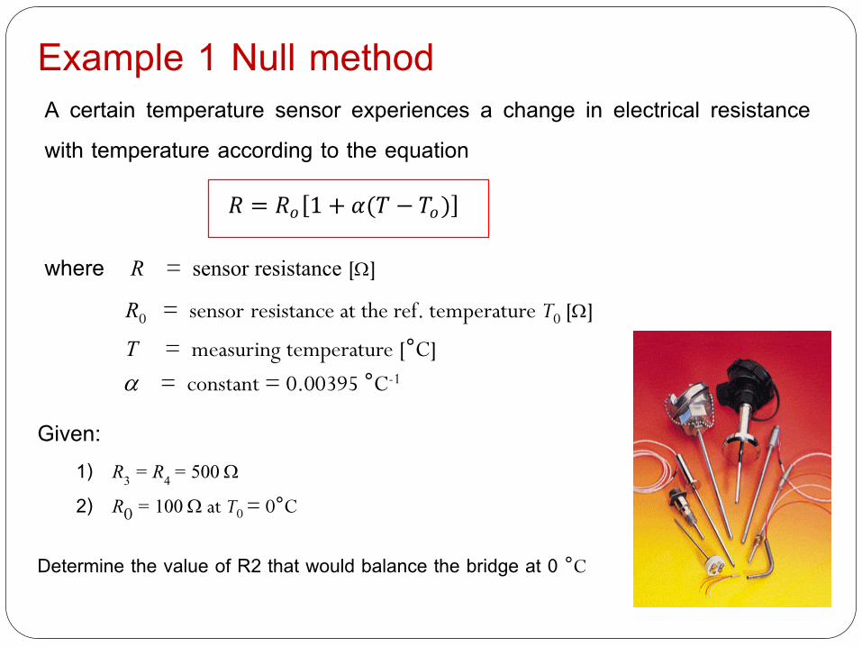
A certain temperature sensor experiences a change in electrical resistance with temperature according to the equation
Example 1 Null method
𝑅 = 𝑅𝑜 1 + 𝛼(𝑇 − 𝑇𝑜)
where R = sensor resistance [W]
R0 = sensor resistance at the ref. temperature T0 [W]
T = measuring temperature [°C]
a = constant = 0.00395 °C-1
Given:1) R3 = R4 = 500 W
2) R0 = 100 W at T0 = 0°C
Determine the value of R2 that would balance the bridge at 0 °C
R1
R3 = R4 = 200 W
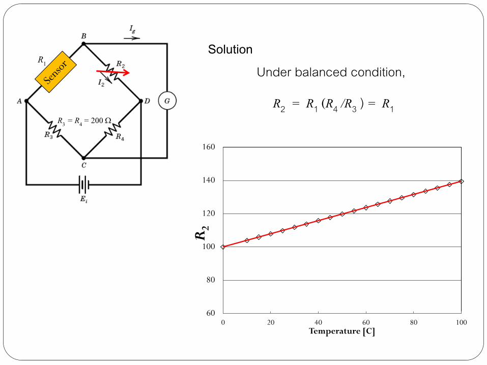
SolutionUnder balanced condition,
R2 = R1 (R4 /R3 ) = R1
60
80
100
120
140
160
0 20 40 60 80 100
R2
Temperature [C]
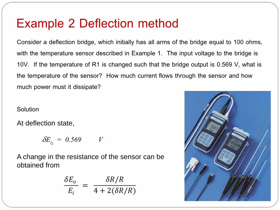
Example 2 Deflection methodConsider a deflection bridge, which initially has all arms of the bridge equal to 100 ohms, with the temperature sensor described in Example 1. The input voltage to the bridge is 10V. If the temperature of R1 is changed such that the bridge output is 0.569 V, what is the temperature of the sensor? How much current flows through the sensor and how much power must it dissipate?
Solution
𝛿𝐸𝑜
𝐸𝑖 =
𝛿𝑅/𝑅
4 + 2(𝛿𝑅/𝑅)
At deflection state,
A change in the resistance of the sensor can be
obtained from
dEo = 0.569 V

We obtain
Therefore, the temperature of the sensor is
By Kirchoff’s law, the current flowing through R1 is
given by
The power dissipated from the sensor is
d R = 25.67 ohms
100 + 25.67 = 100 1 + 0.00395 𝑇 − 0
𝑇 = 65℃
𝐼1 = 𝐸𝑖
1
𝑅1 + 𝛿𝑅 + 𝑅2= 44.3 𝑚𝐴
𝑃1 = 𝐼12 𝑅1 + 𝛿𝑅 = 0.25 𝑊
𝑅1 = 𝑅0 + 𝛿𝑅 = 𝑅0[1 + 0.00395(𝑇 − 𝑇0)]
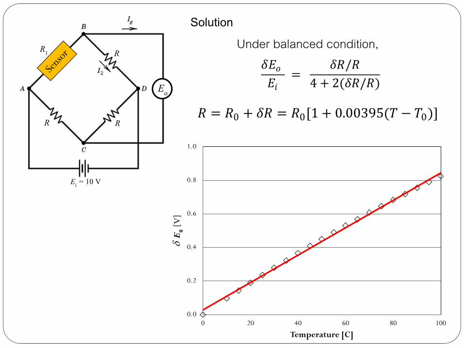
0.0
0.2
0.4
0.6
0.8
1.0
0 20 40 60 80 100
dE 0
[V]
Temperature [C]
R1
Ei = 10 V
R
RR
EEo
SolutionUnder balanced condition,
𝛿𝐸𝑜
𝐸𝑖 =
𝛿𝑅/𝑅
4 + 2(𝛿𝑅/𝑅)
𝑅 = 𝑅0 + 𝛿𝑅 = 𝑅0[1 + 0.00395(𝑇 − 𝑇0)]
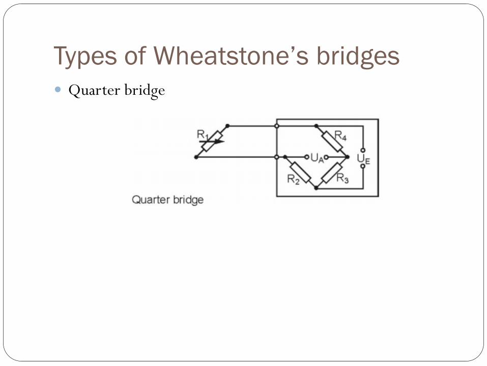
Types of Wheatstone’s bridges
Quarter bridge

3
4
2
1 2
R
R
R
RR K =
2-wire circuit analysis
Initially, where
If then
RRRRR ==== 4321
01 DR
02
4
1
=
R
Rvv K
so
D=
R
RRvv K
so
2
4
1 1
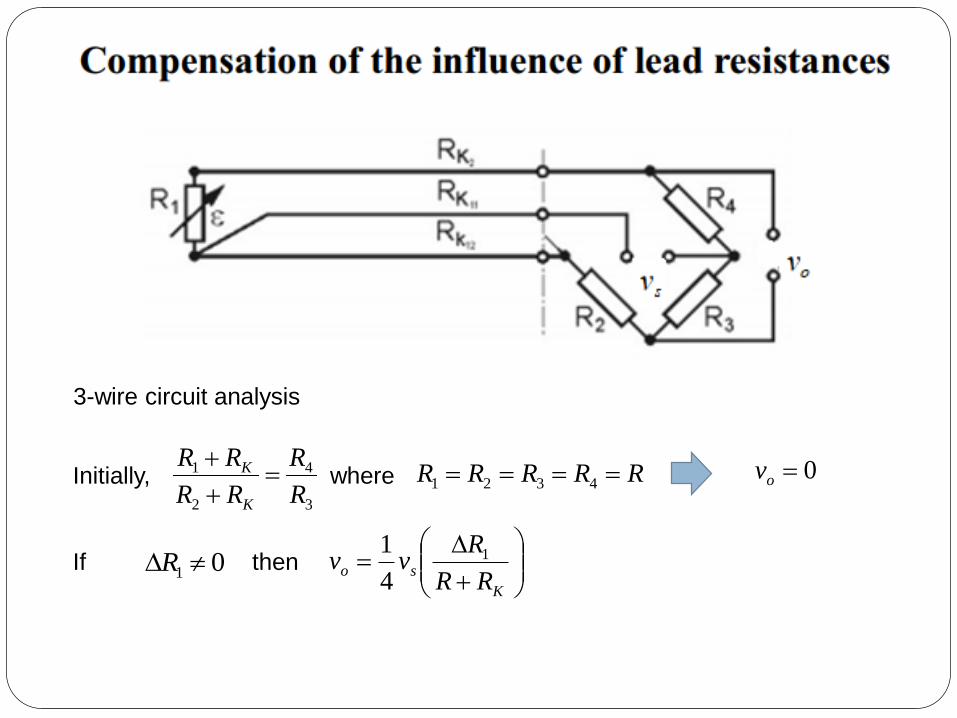
Influence of lead resistances
3
4
2
1
R
R
RR
RR
K
K =
3-wire circuit analysis
Initially, where
If then
RRRRR ==== 43210=ov
01 DR
D=
K
soRR
Rvv 1
4
1

3
4
2
1
R
R
R
R=
2-wire circuit analysis
Initially, where and
If then and
04321 RRRRR ====
TRRRR T D=D= a001
0=ov
D=
1
,4
1
R
Rvv T
sTo
Temperature effects
04321 TTTTT ====
TTT D= 01
DD=
1
1
4
1
R
RRvv T
so

3
4
2
1
R
R
R
R=
Half brigde circuit analysis
Initially, where and
If then and
04321 RRRRR ====
TRRRRR T D=D== a0021
0=ov
04
1
21
, =
D
D=
R
R
R
Rvv TT
sTo
Compensation of Temperature effects
04321 TTTTT ====
TTTT D== 021
D
D=
2
2
1
1
4
1
R
R
R
Rvv so
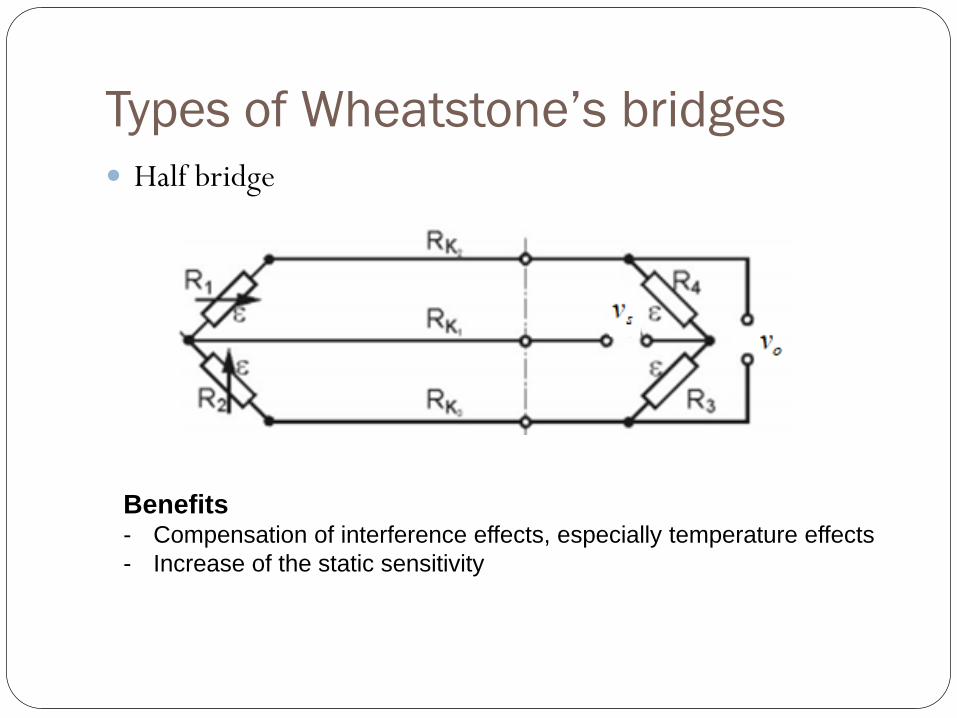
Types of Wheatstone’s bridges
Half bridge
Benefits- Compensation of interference effects, especially temperature effects
- Increase of the static sensitivity

Types of Wheatstone’s bridges
Full bridge
Benefits- Compensation of interference effects, especially temperature effects
- Increase of the static sensitivity

คณะวศวกรรมศาสตรมหาวทยลยธรรมศาสตร Measurement and Instrumentation
Signal Conditioning Circuits
:Amplifiers

Amplifiers Is a device that scales the magnitude of an analog input signal according to
the relation
Input voltage, Vi Output voltage, Vo
Supply voltage, Vs
Vo = G x Vi where G = Gain
0
0.2
0.4
0.6
0.8
1
0 2 4 6 8 10
t
vo
0
0.2
0.4
0.6
0.8
1
0 2 4 6 8 10
t
vi
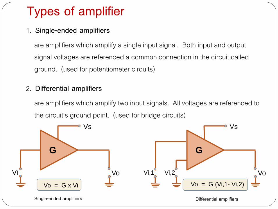
Types of amplifier1. Single-ended amplifiers
are amplifiers which amplify a single input signal. Both input and output signal voltages are referenced a common connection in the circuit called ground. (used for potentiometer circuits)
2. Differential amplifiersare amplifiers which amplify two input signals. All voltages are referenced to the circuit's ground point. (used for bridge circuits)
Vi Vo
Vs
G
Vi,2 Vo
Vs
G
Vi,1
Vo = G x Vi Vo = G (Vi,1- Vi,2)
Single-ended amplifiers Differential amplifiers

Operational Amplifiers (op-amp) An “op-amp” is a high-gain electronic voltage amplifier with a differential
input and, usually, a single-ended output.
Characteristics of op-amps 1. High internal gain G = 105 to 106
2. High input impedance Zi > 107W
3. Low output impedance Zo < 100 W4. two input ports, a noninverting and an inverting input, and one output port
Inverting terminal
Non-inverting terminal
Vo = G (Vnon-inv - Vinv)
(+5V)
(-5V)
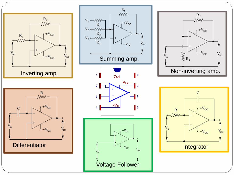
Inverting amp. Non-inverting amp.
Summing amp.
IntegratorDifferentiator
Voltage Follower

𝐺𝑐 =𝑉𝑜𝑉𝑖
≅ −𝑅𝑓
𝑅1
Inverting Amplifier:
Rf
𝑖1 + 𝑖𝑓 = 𝑖𝑎
Circuit analysis
𝑖𝑓 =𝑉𝑜 − 𝑉𝑎
𝑅𝑓 𝑖𝑎 =
𝑉𝑎𝑅𝑎
𝑖1 =𝑉𝑖 − 𝑉𝑎
𝑅1
Sum of currents at Node A
Rf
R1
Ra
Vi
Vo
Vai1
if
iaA
Output voltage of the inverting amplifier
𝑣𝑎 = −𝑉𝑜𝐺

Non-inverting Amplifier:
𝐺𝑐 =𝑉𝑜𝑉𝑖
≅ 1 +𝑅𝑓
𝑅1
Non-inverting
amplifier
iV ico VGV =
Summing Amplifier:
Summing
amplifier
321 ,, VVV
=
3
3,
2
2,
1
1,
R
V
R
V
R
VRV
iii
fo
Voltage follower Amplifier:
Voltage
follower
iV ico VGV =𝐺𝑐 =
𝑉𝑜𝑉𝑖
≅𝐺
1 + 𝐺
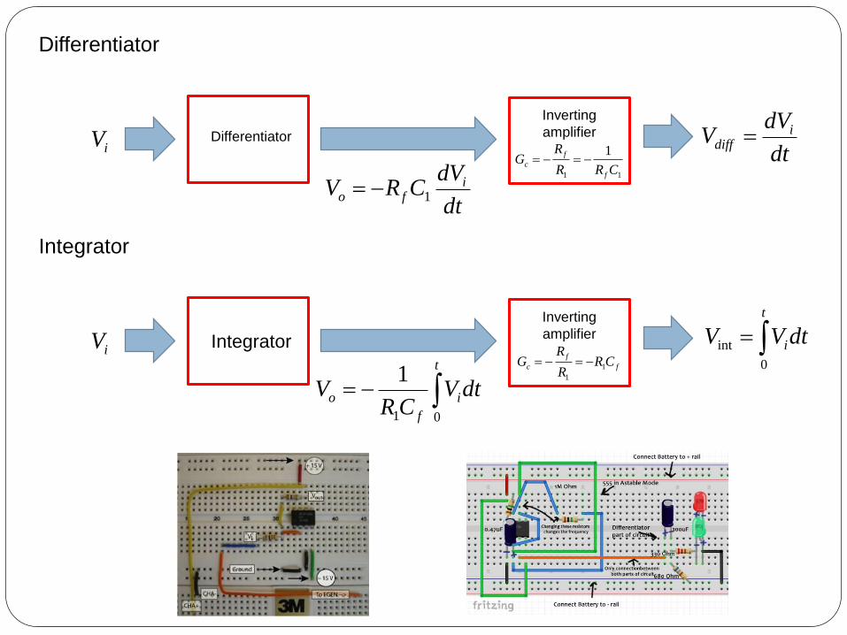
Differentiator
DifferentiatoriV
dt
dVCRV i
fo 1=
Inverting
amplifier
11
1
CRR
RG
f
f
c == dt
dVV i
diff =
Integrator
IntegratoriV
=
t
i
f
o dtVCR
V01
1
Inverting
amplifier
f
f
c CRR
RG 1
1
===
t
idtVV0
int
คณะวศวกรรมศาสตรมหาวทยลยธรรมศาสตร Measurement and Instrumentation
Signal Conditioning Circuits
:Filters

Filters In many instrumentation applications, the (dynamic) signal from the
transducer is combined with noise or some other parasitic signal. These undesired signals can be eliminated with a filter that is designed to attenuate the noise signals but transmit the transducer signal without distortion.
Two filters that utilize passive components and are commonly employed in signal conditioning include (1) High-pass RC filter and (2) Low-pass RC filter
RC filter circuits
R
C
C
R

Filters
Unfiltered signal with low frequency
variation and high frequency noise
High-pass filter
High-pass filter employed to
remove low frequency variation
Low-pass filterFiltered signal
Low-pass filter employed to remove
high frequency noise

High-pass RC filters
High-pass filter permits only frequencies above the cutoff frequency to pass.
𝑉𝑜 =𝜔𝑅𝐶
1 + (𝜔𝑅𝐶)2 𝑉𝑖 𝑒
𝑗𝜔𝑡+𝜙
𝜙 =𝜋
2− 𝑡𝑎𝑛−1(𝜔𝑅𝐶)
where
𝑉𝑜 ~ 0 if w 0
Consider a summation of voltage drops around the loop
𝑉𝑖 −𝑞
𝐶− 𝑅𝑖 = 0
If and𝑉𝑖 = 𝑉𝑖 𝑒𝑗𝜔𝑡 𝑞 = 𝑖
𝑡
0
𝑑𝑡
The output voltage Vo is
High pass
Passband
Stopband

Low-pass filters Low-pass filter permits only frequencies below the cutoff frequency to pass while
blocking the passage of frequency information above the cut off frequency.
where
𝑉𝑜 ~ 0 ถา w
The output voltage is
𝑉𝑜 =1
1 + (𝜔𝑅𝐶)2 𝑉𝑖 𝑒
𝑗𝜔𝑡−𝜙
𝜙 = 𝑡𝑎𝑛−1(𝜔𝑅𝐶)
Passband
Stopband

Cut-off frequency is defined as the frequency at which the ratio of the amplitudes of the output to the
input has a magnitude of 0.02 (2% error). For examples,
(1) Hi-pass filter
(2) Lo-pass filter
|Vo|/|Vi| = wCRC/[1+(wCRC)2]1/2 = 0.02 wC = 5/RC fC = 5/(2pRC)
|Vo|/|Vi| = 1/[1+(wCRC)2]1/2 = 0.02 wC = 0.203/RC fC = 0.203/(2pRC)
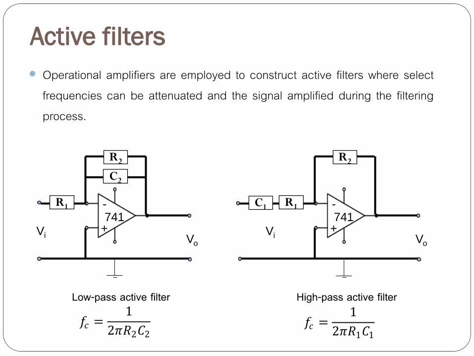
Active filters
Operational amplifiers are employed to construct active filters where select frequencies can be attenuated and the signal amplified during the filtering process.
741+
-R1
R2
C2
Vi Vo
741+
-R1
R2
Vi Vo
C1
Low-pass active filter High-pass active filter
𝑓𝑐 =1
2𝜋𝑅2𝐶2 𝑓𝑐 =
1
2𝜋𝑅1𝐶1

คณะวศวกรรมศาสตรมหาวทยลยธรรมศาสตร Measurement and Instrumentation
Signal Conditioning Circuits
:Modulators and Demodulators

Amplitude Modulators Amplitude modulation is a signal conditioning process in which the
signal from a transducer is multiplied by a carrier signal of constant frequency and amplitude.
Transducer signal(sinusoidal, transient, or random)
Carrier signal(sinusoidal, transient, or random)x
𝑉𝑖(𝑡) = 𝑣𝑖sin(𝜔𝑖𝑡) 𝑉𝑐(𝑡) = 𝑣𝑐sin(𝜔𝑐𝑡)
𝜔𝑐 ~ 10 − 100 𝜔𝑖
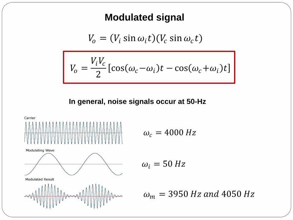
𝑉𝑜 = 𝑉𝑖 sin 𝜔𝑖𝑡 (𝑉𝑐 sin 𝜔𝑐𝑡)
𝑉𝑜 =𝑉𝑖𝑉𝑐
2 cos 𝜔𝑐−𝜔𝑖 𝑡 − cos 𝜔𝑐+𝜔𝑖 𝑡
Modulated signal
𝜔𝑐 = 4000 𝐻𝑧
In general, noise signals occur at 50-Hz
𝜔𝑚 = 3950 𝐻𝑧 𝑎𝑛𝑑 4050 𝐻𝑧
𝜔𝑖 = 50 𝐻𝑧

Amplitude Modulators
Advantages(1) Stability(2) Low power(3) Noise suppression
Demodulation is the process that the transducer signal is separated from the carrier signal.
Rectifier Filter

Assignment #3
1. Shown that the output voltage of the summing amplifier be expressed by the equation
2. Consider the Wheatstone bridge. Suppose R3 = R4 = 200 W, R2 = variable calibrated resistor, and R1 = transducer resistance = 40x + 100
a) When x = 0, what is the value of R2 required to balance the bridge?
b) If the bridge is operated in a balanced condition in order to measure x, determine the relationship between R2 and x.
𝑉𝑜 = −𝑅𝑓 𝑉𝑖,1
𝑅1+
𝑉𝑖,2
𝑅2+
𝑉𝑖,3
𝑅3

คณะวศวกรรมศาสตรมหาวทยลยธรรมศาสตร Measurement and Instrumentation
Fundamental of Sampling, Data
Acquisition and Digital Devices

Sampling concepts
Conversion of analog signals to digital code is extremely importantin any instrument system that involves digital processing of the analogoutput signals from the signal conditioners.
Continuous
Signal
Discrete
Signal
“discrete time series”

Discrete time series
Suppose the transducer signal is measured repeatedly at successive sample time increments dt
𝑦(𝑟𝛿𝑡) = 𝑦 𝑡 𝛿(𝑡 − 𝑟𝛿𝑡) 𝑟 = 1, 2, 3, … , 𝑁
sample rate
total sample period
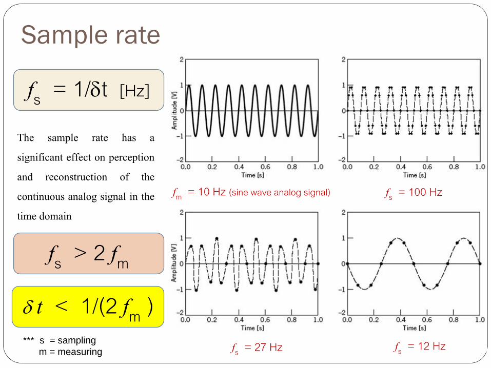
fs = 1/dt [Hz]
Sample rate
The sample rate has a significant effect on perception and reconstruction of the continuous analog signal in the time domain
fs > 2 fm
*** s = sampling
m = measuring
fm = 10 Hz (sine wave analog signal) fs = 100 Hz
fs = 27 Hz fs = 12 Hz
d t < 1/(2 fm )

Alias Frequencies
When the sample rate is less than 2fm , the higher frequency content of the analog signal will take on the false identity of a lower frequency in the resulting discrete series. A false frequency is called an “alias frequency”.
Original signal10 Hz 2 Hz
sample rate 12 Hz
Interpreted signal

is the diagram that is used to
find the alias frequency.
Example
f = 10 Hz
fN = 6 Hz
Folding Diagram
[f/fN]y-axis= 10/6 = 1.67
0.33
[f/fN]x-axis = 0.33 Hz
1.67
falias = 0.33 x fN = 2 Hz

Nyquist frequency and Anti-Aliasing
Nyquist frequency is the highest frequency that can be coded at a given sampling rate in order to be able to fully reconstruct the signal,
Anti-aliasing is a process that remove signal content at and above Nyquist frequency by use of a low-pass filter prior to sampling and use an appropriate sample rate for the signal
fN = 0.5 fs
Signal = Signal [f < fN ] + Signal [f > fN ]
Anti-aliasing filter
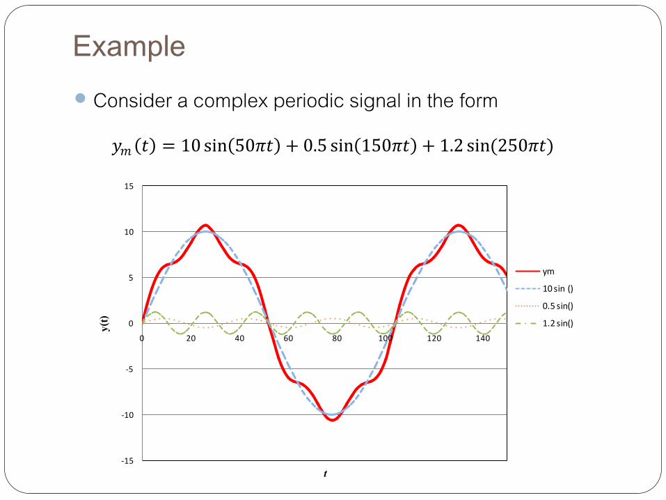
Example Consider a complex periodic signal in the form
-15
-10
-5
0
5
10
15
0 20 40 60 80 100 120 140
y(t)
t
ym
10 sin ()
0.5 sin()
1.2 sin()
𝑦𝑚 𝑡 = 10 sin 50𝜋𝑡 + 0.5 sin 150𝜋𝑡 + 1.2 sin(250𝜋𝑡)

Example (cont.) If the signal is sampled at 100 Hz
Observe all frequency content in the sampled signal
fN = 0.5 fs = 0.5 x 100 Hz = 50 Hz
f1 = 25 Hz f2 = 75 Hz f3 = 125 Hz
fN < fm Alias frequency
𝑦𝑚 𝑡 = 10 sin 50𝜋𝑡 + 0.5 sin 150𝜋𝑡 + 1.2 sin(250𝜋𝑡)

-15
-10
-5
0
5
10
15
0 20 40 60 80 100 120 140
y(t)
t
ys
ym
10 sin ()
Example (Cont.) Sampled signal
Alias frequency = 25 Hz
𝑦𝑠 𝑟𝛿𝑡 = 10 sin 50𝜋𝑟𝛿𝑡 + 0.5 sin 50𝜋𝑟𝛿𝑡 + 1.2 sin(50𝜋𝑟𝛿𝑡)
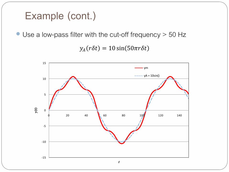
Example (cont.) Use a low-pass filter with the cut-off frequency > 50 Hz
𝑦𝐴 𝑟𝛿𝑡 = 10 sin 50𝜋𝑟𝛿𝑡
-15
-10
-5
0
5
10
15
0 20 40 60 80 100 120 140
y(t)
t
ym
yA = 10sin()
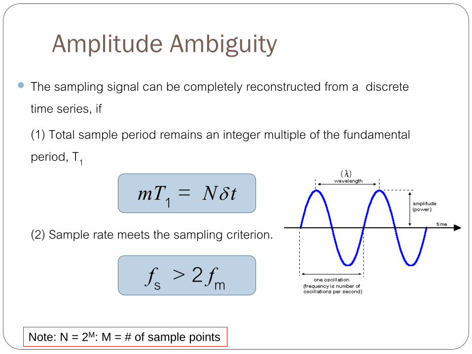
Amplitude Ambiguity
The sampling signal can be completely reconstructed from a discrete time series, if (1) Total sample period remains an integer multiple of the fundamental period, T1
(2) Sample rate meets the sampling criterion.
fs > 2 fm
mT1 = Nd t
Note: N = 2M: M = # of sample points

Amplitude spectra
Example
Amplitude = 10Fundamental period T1 =1/ 100 s
(a) m = N dt / T1 = 2.56
(b) m = N dt / T1 = 10.24
(c) m = N dt / T1 = 8
No leakage
amplitude leakage
amplitude leakage
𝑦 𝑡 = 10cos(2𝜋100𝑡)
(8-bit)
d f = (Nd t)-1 = fs/N = 39 Hz

Selecting sample rate and data number
For an exact discrete representation in both frequency and amplitude of analog signal, both the number of data points and the sample rate should be chosen based on the following criteria: (1) fs > 5 fm (2) long total sample periods (large N) and (3) use of anti-alias filter.
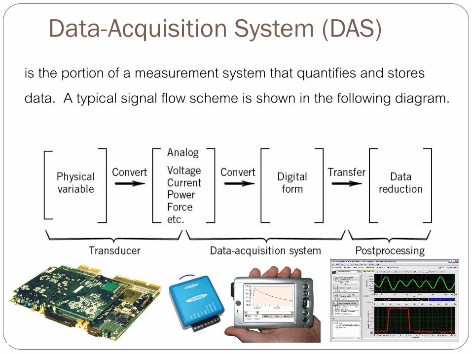
Data-Acquisition System (DAS)
is the portion of a measurement system that quantifies and stores data. A typical signal flow scheme is shown in the following diagram.

Signal flow scheme for an automated data-acquisition system
Data-Acquisition System components
A/D
converter
Signal Conditioning: Filters and
Amplification
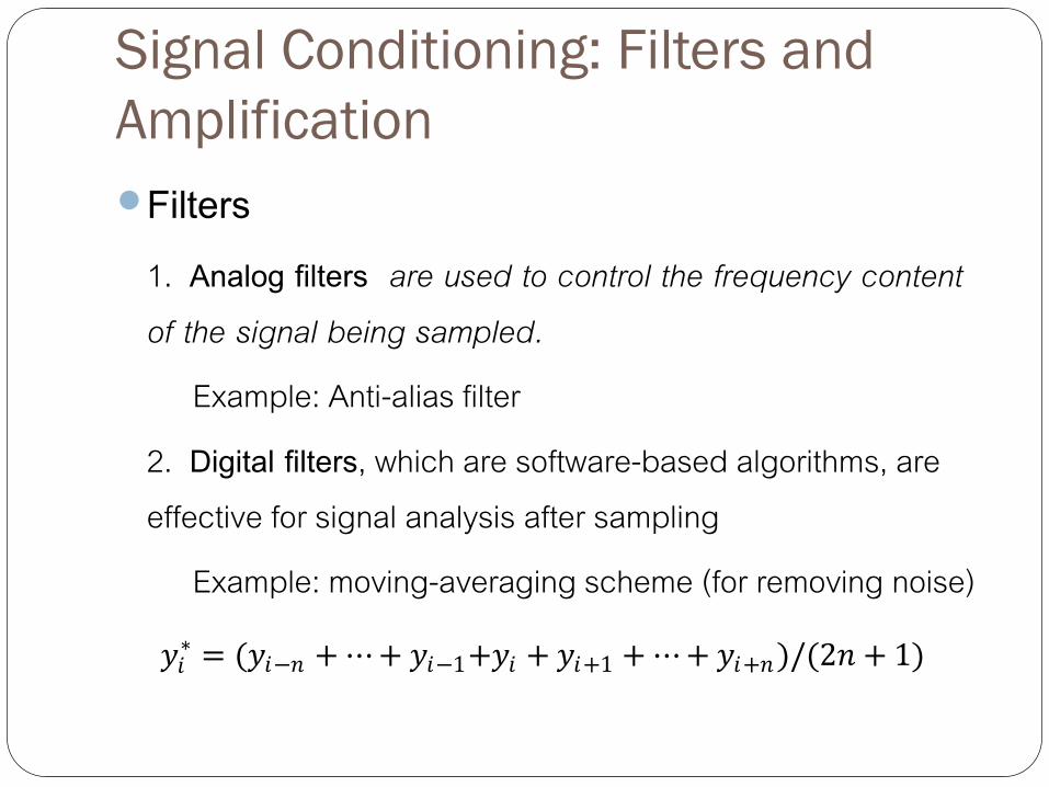
Filters1. Analog filters are used to control the frequency content of the signal being sampled.
Example: Anti-alias filter2. Digital filters, which are software-based algorithms, are effective for signal analysis after sampling
Example: moving-averaging scheme (for removing noise)
𝑦𝑖∗ = (𝑦𝑖−𝑛 + ⋯ + 𝑦𝑖−1+𝑦𝑖 + 𝑦𝑖+1 + ⋯ + 𝑦𝑖+𝑛)/(2𝑛 + 1)

Signal Conditioning: Filters and
Amplification
AmplifiersAll DASs are input range limited; that is, there is a minimum value and a maximum value of signal. Some transducer signals will need amplification or attenuation prior to conversion. Most DASs contain on-board instrumentation amplifiers.
0-50 V signal 0-10 V A/D converter
Voltage divider
for signal attenuation
R1 = 40 kW
R2 = 10 kW

Signal Conditioning: Filters and
Amplification
Shunt circuitsAn A/D converter requires a voltage signal at its input. It is straightforward to convert current signals into voltage signals using a shunt resistor.
In general, the standard
current signal has a range of
4 – 20 mA
Using a shunt resistor = 250 W, the current signal would be
converted into the voltage signal
1 – 5 V

Signal Conditioning: Filters and
Amplification
MultiplexerWhen multiple input signal lines are connected by a common
throughout line to a single A/D converter, a multiplexer is used to switch between connections, one at a time.

A/D Convertersconvert the analog signals into the digital signals with conversion rates typically up to the 1 kHz – 10 MHz range . The input resolution, Q which depends on the number of bits of the converter, is given by
𝑄 =𝐸𝐹𝑆𝑅
2𝑀
where EFSR = Full scale voltage range
M = resolution in bits
Example A12 bit A/D converter
with input signal range of 0-10V.
The resolution
Q = 10/212 = 2.44 mV
The amplifier permits signal
conditioning with gains from G =
0.5 to 1000
The minimum detectable voltage
when set at maximum gain is
Q = 2.44 mV / 1000 = 2.44 mV3-bits resolution
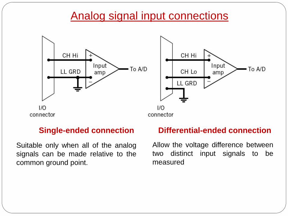
Single-ended connection Differential-ended connection
Suitable only when all of the analog
signals can be made relative to the
common ground point.
Allow the voltage difference between
two distinct input signals to be
measured
Analog signal input connections

Example
A signal from the strain gage with the sensitivity = 2.5mV/me is connected to DAS which has the 12-bit A/D converter, an input range of ± 5V, and sample rate of 1000 Hz. For an expected measurement range of 1-500 me, specify appropriate G for amplifier, filter type and cut-off frequency.
VO
Vi
+ -
Strain gage (Rg) , S = 2.5mV/me
signal
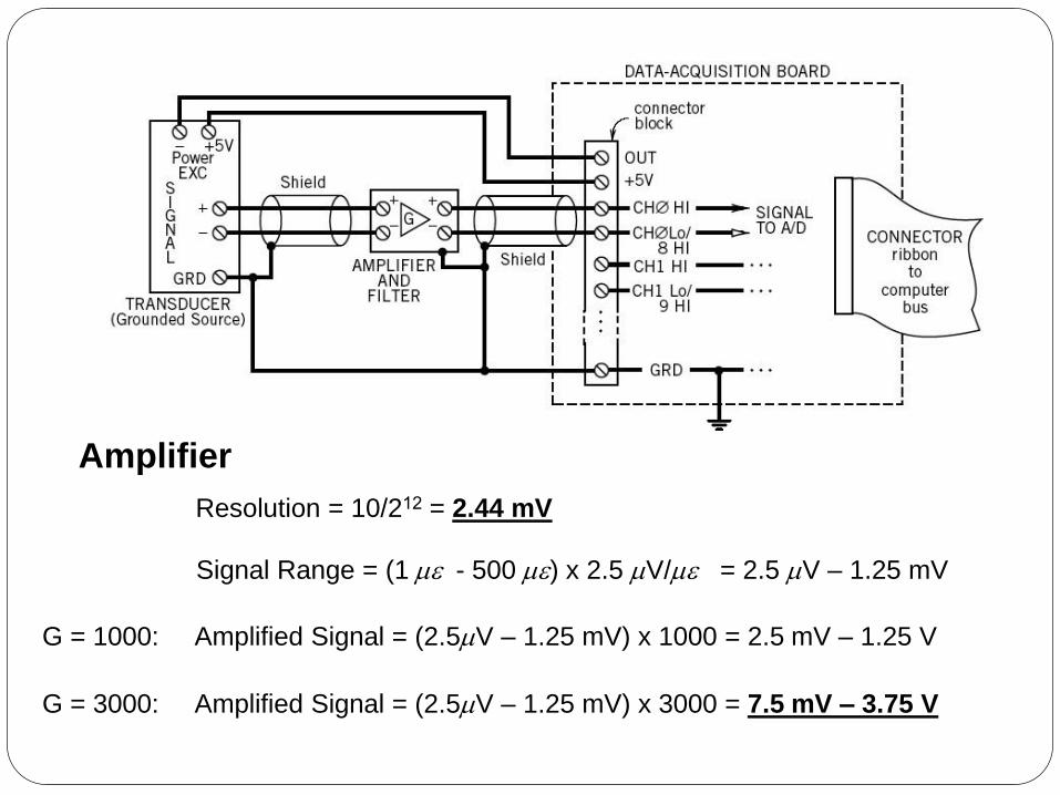
Resolution = 10/212 = 2.44 mV
Amplifier
Signal Range = (1 me - 500 me) x 2.5 mV/me = 2.5 mV – 1.25 mV
G = 1000: Amplified Signal = (2.5mV – 1.25 mV) x 1000 = 2.5 mV – 1.25 V
G = 3000: Amplified Signal = (2.5mV – 1.25 mV) x 3000 = 7.5 mV – 3.75 V

Sample rate, fs = 1000 Hz
Filter
Nyquist frequency , fN = 1000/2 = 500 Hz
*** Low-pass filter with a cut-off frequency = 500 Hz required
*** Differential-ended connections required

Final Examination on OCT 8, 2011 (1300-1600)
Closed books and closed notes
Non-programmable calculators are permitted
Electronic dictionaries are not permitted
7 questions (10 marks each)

Data Logger
คออปกรณอเลคทรอนคสซงท ำหนำทบนทกและจดเกบขอมลทตรวจวดจำกเครองมอวดหรอเซนเซอรตำงๆ ปจจบน Data logger ใชพนฐำนของระบบประมวลผลแบบดจตอล สวนประกอบทส ำคญคอ ไมโครโปรเซสเซอร หนวยควำมจ ำ และเซนเซอร สำมำรถแบงออกไดเปน 2ลกษณะคอ
- General purpose types
- Specific devices
ขอด 1. ท ำงำนดวยตวเอง (Stand-alone)2. เคลอนยำยงำย (Portable)3. บนทกขอมล 24 ชวโมง4. สำมำรถใชกบ DC power
http://www.dataq.com/images/products/data-logger/gl200_500w.jpg

ตวอยาง Data logger

ตวอยาง ขอมลจ าเพาะ Data logger

ตวอยาง ขอมลจ าเพาะ Data logger (ตอ)
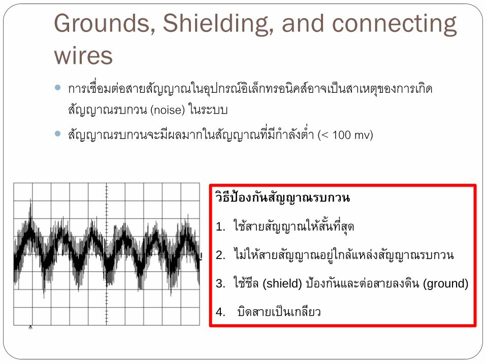
Grounds, Shielding, and connecting
wires การเชอมตอสายสญญาณในอปกรณอเลกทรอนคสอาจเปนสาเหตของการเกดสญญาณรบกวน (noise) ในระบบ
สญญาณรบกวนจะมผลมากในสญญาณทมก าลงต า (< 100 mv)
วธปองกนสญญาณรบกวน
1. ใชสายสญญาณใหสนทสด
2. ไมใหสายสญญาณอยใกลแหลงสญญาณรบกวน
3. ใชชล (shield) ปองกนและตอสายลงดน (ground)
4. บดสายเปนเกลยว

Ground and Ground loop
Ground คอจดอางองในวงจรไฟฟาใชในการเปรยบเทยบแรงดนไฟฟา โดยทวไป Ground จะเปนเสนทางเดนของกระแสลงสพนดน ( earth ground) ซงมคาแรงดนไฟฟาเทากบศนย
Ground potential อาจมคาตางกนขนกบจดเชอมตอ (เชน อปกรณ อาคาร และพนดน)
สายดนทความยาวมากๆ อาจเปนท าหนาทเหมอนกบ เสาอากาศ (Antennae)
Signal
ground
Chassis
ground
Earth
ground
Ground Symbols
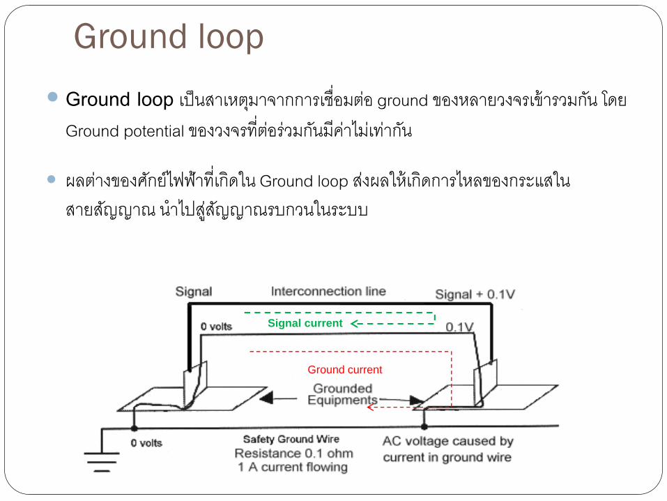
Ground loop
Ground loop เปนสาเหตมาจากการเชอมตอ ground ของหลายวงจรเขารวมกน โดยGround potential ของวงจรทตอรวมกนมคาไมเทากน
ผลตางของศกยไฟฟาทเกดใน Ground loop สงผลใหเกดการไหลของกระแสในสายสญญาณ น าไปสสญญาณรบกวนในระบบ
Signal current
Ground current
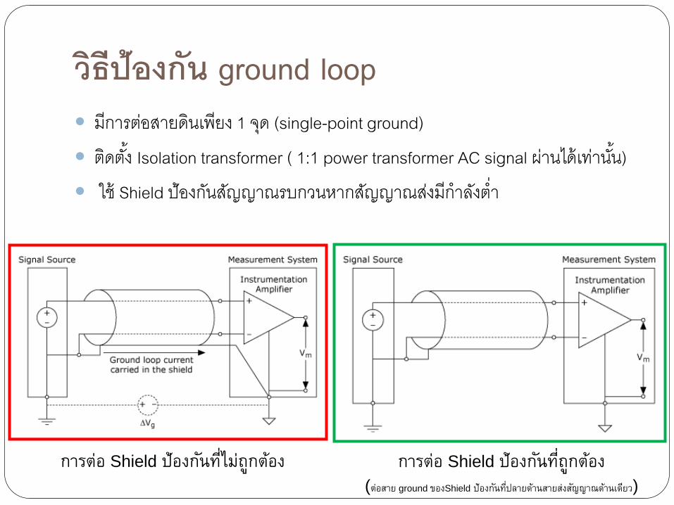
วธปองกน ground loop มการตอสายดนเพยง 1 จด (single-point ground) ตดตง Isolation transformer ( 1:1 power transformer AC signal ผานไดเทานน) ใช Shield ปองกนสญญาณรบกวนหากสญญาณสงมก าลงต า
การตอ Shield ปองกนทไมถกตอง การตอ Shield ปองกนทถกตอง(ตอสาย ground ของShield ปองกนทปลายดานสายสงสญญาณดานเดยว)