sigma-delta modulation for ad conversion in radio receivers
DESCRIPTION
This book describes the theory, design and realizations of continuous-timemodulators for analog-to-digital conversion in radio receivers. The challenge ofthe work is the design of a modulator with high linearity, large dynamic rangeand strong image rejection capabilities. With such an A/D converter, requirementsfor a receiver architecture in terms of selectivity and sensitivity can be relaxed,resulting in a cheaper system with a higher level of integration.TRANSCRIPT


CONTINUOUS-TIME SIGMA-DELTA MODULATIONFOR A/D CONVERSION IN RADIO RECEIVERS

THE KLUWER INTERNATIONAL SERIESIN ENGINEERING AND COMPUTER SCIENCE
ANALOG CIRCUITS AND SIGNAL PROCESSINGConsulting Editor: Mohammed Ismail. Ohio State University
Related Titles:
DIRECT DIGITAL SYNTHESIZERS: THEORY, DESIGN AND APPLICATIONSJ. Vankka, K. HalonenISBN: 0-7923 7366-9
SYSTEMATIC DESIGN FOR OPTIMISATION OF PIPELINED ADCsJ. Goes, J.C. Vital, J. FrancaISBN: 0-7923-7291-3
OPERATIONAL AMPLIFIERS: Theory and DesignJ. HuijsingISBN: 0-7923-7284-0
HIGH-PERFORMANCE HARMONIC OSCILLATORS AND BANDGAP REFERENCESA. van Staveren, C.J.M. Verhoeven, A.H.M. van RoermundISBN: 0-7923-7283-2
HIGH SPEED A/D CONVERTERS: Understanding Data Converters Through SPICEA. MoscoviciISBN: 0-7923-7276-X
ANALOG TEST SIGNAL GENERATION USING PERIODIC ENCODED DATASTREAMS
B. Dufort, G.W. RobertsISBN: 0-7923-7211-5
HIGH-ACCURACY CMOS SMART TEMPERATURE SENSORSA. Bakker, J. HuijsingISBN: 0-7923-7217-4
DESIGN, SIMULATION AND APPLICATIONS OF INDUCTORS AND TRANSFORMERSFOR Si RF ICs
A.M. Niknejad, R.G. MeyerISBN: 0-7923-7986-1
SWITCHED-CURRENT SIGNAL PROCESSING AND A/D CONVERSION CIRCUITS:DESIGN AND IMPLEMENTATION
B.E. JonssonISBN: 0-7923-7871-7
RESEARCH PERSPECTIVES ON DYNAMIC TRANSLINEAR AND LOG-DOMAINCIRCUITS
W.A. Serdijn, J. MulderISBN: 0-7923-7811-3
CMOS DATA CONVERTERS FOR COMMUNICATIONSM. Gustavsson, J. Wikner, N. TanISBN: 0-7923-7780-X
DESIGN AND ANALYSIS OF INTEGRATOR-BASED LOG -DOMAIN FILTER CIRCUITSG.W. Roberts, V. W. LeungISBN: 0-7923-8699-X
VISION CHIPSA. MoiniISBN: 0-7923-8664-7
COMPACT LOW-VOLTAGE AND HIGH-SPEED CMOS, BiCMOS AND BIPOLAROPERATIONAL AMPLIFIERS
K-J. de Langen, J. HuijsingISBN: 0-7923-8623-X

CONTINUOUS-TIMESIGMA-DELTA MODULATION
FOR A/D CONVERSION INRADIO RECEIVERS
by
Lucien BreemsPhilips Research, Eindhoven, The Netherlands
and
Johan H. HuijsingDelft University of Technology, The Netherlands
KLUWER ACADEMIC PUBLISHERSNEW YORK, BOSTON, DORDRECHT, LONDON, MOSCOW

eBook ISBN: 0-306-48004-2Print ISBN: 0-7923-7492-4
©2002 Kluwer Academic PublishersNew York, Boston, Dordrecht, London, Moscow
Print ©2001 Kluwer Academic Publishers
All rights reserved
No part of this eBook may be reproduced or transmitted in any form or by any means, electronic,mechanical, recording, or otherwise, without written consent from the Publisher
Created in the United States of America
Visit Kluwer Online at: http://kluweronline.comand Kluwer's eBookstore at: http://ebooks.kluweronline.com
Dordrecht
Table of contents
List of abbreviations ix
List of symbols
Preface
xi
1 Introduction
1.11.21.31.41.5
The world of communicationSigma-delta A/D conversionSystem level simulationMotivation and objectivesOrganization of the workReferences
2 A/D conversion in radio receivers
2.12.2
IntroductionFrom baseband to RF A/D conversion
2.2.12.2.22.2.3
Heterodyne receiver with baseband A/D conversionHeterodyne receiver with IF digitizingReceiver architecture with RF digitizing
2.32.4
Sigma-delta modulation in a heterodyne receiverPerformance parameters
2.4.12.4.22.4.32.4.4
Dynamic rangeLinearityImage rejectionFigure-of-merit
2.52.6
GSM and AM/FM radio specificationsSummaryReferences
1
135668
9
910111314141616171921222426
CONTINUOUS-TIME MODULATION FOR A/D CONVERSION IN RADIO RECEIVERS V
xiii

Table of contents
3 Continuous-time sigma-delta modulation 293.13.2
IntroductionTheory of sigma-delta modulation
3.2.13.2.23.2.33.2.43.2.53.2.6
Oversampling and noise-shapingTonesHarmonic distortionIntersymbol interferencePhase jitterAliasing
3.3 Linear stability analysis3.3.1 Small signal stability
Large signal stability3.3.23.4 High-frequency stability compensation
3.4.13.4.23.4.33.4.43.4.5
Feedforward compensationFeedforward compensation and local feedbackFeedback compensationFeedback compensation and local feedbackFeedforward versus feedback compensation
3.5 Quadrature sigma-delta modulation3.5.13.5.2
Complex integratorComplex filter design
References
4 Realization of an IF-to-baseband sigma-deltamodulator4.14.2
IntroductionFrequency translation in sigma-delta modulators
4.2.14.2.24.2.3
Mixer inside the sigma-delta loopMixer outside the sigma-delta loopMixer inside loop versus outside loop
4.3 IF mixer design4.3.14.3.24.3.34.3.4
Mixer topologyLinearity performanceLocal oscillator driverSelf-mixing
4.4 IF sigma-delta modulator design4.4.14.4.2
IF sigma-delta modulator topologyInput filter stage design
VI CONTINUOUS-TIME MODULATION FOR A/D CONVERSION IN RADIO RECEIVERS
293030333741434446465153535960616364646670
7373747477787979808288909092

Table of contents
4.4.34.4.44.4.5
Transconductance-C integratorA/D and D/A converterLO driver scheme
4.5 Experimental results4.5.14.5.24.5.3
Test chip 1: Baseband sigma-delta modulatorTest chip 2: IF-to-baseband sigma-delta modulatorPerformance summary
4.6 ConclusionsReferences
5 Realization of a quadrature sigma-deltamodulator5.15.25.3
IntroductionImage interferenceDynamic element matching
5.3.15.3.25.3.35.3.4
Complex data-controlled DEM algorithmDEM implementationImpedance mismatch of DEM and DAC switchesCharge injection of DEM and DAC switches
5.4 Quadrature sigma-delta modulator design5.4.15.4.25.4.3
TopologyInput stageFeedback and DEM circuit
Experimental results5.55.6 Conclusions
References
6 Benchmark
6.16.26.3
IntroductionBenchmark of test chipsConclusionsReferences
Index
96979899
100102105106108
109109110111117118123125129129131132135139141
143
143144147149
153
CONTINUOUS-TIME MODULATION FOR A/D CONVERSION IN RADIO RECEIVERS VII

List of abbreviations
A/DADCAGCAMBERBWCLKCMCTD/ADACDEMDLLDRDSPEXORFFTFMFOMGMSKHDIIFIMIPIRLNALOLSBNTFNZIFOPAMPOSRP
analog-to-digitalanalog-to-digital converterautomatic gain controlamplitude modulationbit error ratebandwidthclockcross-modulationcontinuous-timedigital-to-analogdigital-to-analog converterdynamic element matchingdelay-locked loopdynamic rangedigital signal processorexclusive-orfast fourier transformfrequency modulationfigure-of-meritgaussian minimum-shift-keyingharmonic distortionin-phaseintermediate frequencyintermodulation distortionintercept pointimage rejectionlow-noise amplifierlocal oscillatorleast significant bitnoise transfer functionnear-zero-IFoperational amplifieroversampling ratiopower
IXCONTINUOUS-TIME MODULATION FOR A/D CONVERSION IN RADIO RECEIVERS
List of abbreviations
PLL
QRFRTZSAWSTF
SFDRSINADSNDRSNRSQNRV/IZIF
phase-locked loopquadrature-phaseradio frequencyreturn-to-zerosurface acoustic wavesignal transfer functionsigma-deltaspurious-free dynamic rangesignal-to-noise-and-distortionsignal-to-noise-and-distortion ratiosignal-to-noise ratiosignal-to-quantization-noise ratiovoltage-to-currentzero-IF
X CONTINUOUS-TIME MODULATION FOR A/D CONVERSION IN RADIO RECEIVERS

List of symbols
relative error -relative gain error -phase error rad,°quantization step size -duty cycle -phase rad,°quantizer gain -minimum (large signal) stable quantizer gain -charge carrier mobilitypi, 3.141593 -quantizer phase °standard deviation -time constant sunity gain frequency rad/szero frequency rad/sDC gain -
butterworth coefficient -feedback coefficient -
symbol for capacitor Fdrain-bulk capacitor Fdrain-source capacitor Fgate-drain capacitor Fgate-source capacitor Fintegration capacitor Fnormalized oxide capacitance F
feedforward coefficient -local feedback coefficient -
quantization error -frequency Hz, rad/sbandwidth Hzlocal oscillator frequency Hzsampling frequency Hztransconductance Sloopfilter transfer function -bias current A
CONTINUOUS-TIME MODULATION FOR A/D CONVERSION IN RADIO RECEIVERS XI

List of symbols
offset currentDAC currentsmall signal currenttransient DAC currenttransient input currentresidue currentcomplex operator -Boltzmanns’ constant,channel length of MOS transistoroversampling ratio -jitter powerquantization noise powerthermal noise powerpowerinput powerchargequantization level -return-to-zero duty cycle -DAC resistorinput resistorload resistordegeneration resistorswitch ON-impedanceLaplace operatortemperaturesampling periodtimepositive supply voltage of MOS circuitsnegative supply voltage of MOS circuitsDAC voltagetransient DAC voltagedrain-source voltagegate-to-ground voltage of MOS transistorgate-source voltageeffective gate-source voltageinput voltagetransient input voltageoffset voltageresidue voltagethreshold voltagechannel width of MOS transistor
XII
WWWWWC
rad/sKssVVVVVVVVVVVVV
CONTINUOUS-TIME MODULATION FOR A/D CONVERSION IN RADIO RECEIVERS
AAAAAA
J/K

Preface
This book describes the theory, design and realizations of continuous-timemodulators for analog-to-digital conversion in radio receivers. The challenge ofthe work is the design of a modulator with high linearity, large dynamic rangeand strong image rejection capabilities. With such an A/D converter, requirementsfor a receiver architecture in terms of selectivity and sensitivity can be relaxed,resulting in a cheaper system with a higher level of integration.
Important trends in the receiver design for wireless portable applications are:smaller product sizes, cheaper products and longer stand-by times. Products canbe made smaller and cheaper by increasing the level of integration. This meanson-chip integration of external components, such as inductors and filters. Herein,an important role can be played by the A/D converter. Shifting the A/D convertertowards the antenna side of the receiver, allows more digital integration of(external) analog functions on a single digital chip. However, this requires an A/Dconverter with high linearity, dynamic range, bandwidth and image rejectioncapabilities.
In chapter 2, it will be shown that the required performance of the ADC dependsvery much on its place in the receiver architecture. Single-bit continuous-timemodulation is a good technique for A/D conversion in receivers, as it incorporatesinherent anti-aliasing filtering, excellent linearity performance, and low-powercapability. All these performance aspects are particularly important in battery-powered receivers. The main performance parameters are described and a figure-of-merit is presented that is used for comparison between different designs.
In chapter 3, the theory of higher-order continuous-time modulation isdescribed. Important aspects, determining the performance of a continuous-time
modulator, are quantization noise, DC tones, intersymbol interference, clockjitter, and aliasing. The design of higher-order filters is described, withButterworth and inverse-Chebyshev filter characteristics. With the availability ofquadrature signals in a radio receiver, the theory of quadrature modulation istreated as well.
Chip realizations are described in chapter 4 and chapter 5. Chapter 4 describes thedesign of a modulator with integrated mixer. The key features of this IF-to-
CONTINUOUS-TIME MODULATION FOR A/D CONVERSION IN RADIO RECEIVERS XIII

Preface
baseband A/D converter are the high linearity and low-power consumption. Inchapter 5 the design of a quadrature modulator with a data-dependentdynamic element matching circuit is shown. Measurements on this A/D convertershow a high image rejection of 63 dB typically.
In the last chapter the main conclusions are summarized. The performance of theprototype test chips that have been described in this book are compared with otherstate-of-the-art test designs from literature.
The authors wish the reader a pleasant time in investigating the interesting aspectsof continuous-time modulation for A/D conversion in radio receivers.
Lucien J. BreemsJohan H. Huijsing
Eindhoven, May 2001
XIV CONTINUOUS-TIME MODULATION FOR A/D CONVERSION IN RADIO RECEIVERS
Introduction
This book describes the theory, design and realization of continuous-time sigma-delta modulators for analog-to-digital (A/D) conversion in radio receivers.The challenge of the work is the design of a modulator with high linearity,large dynamic range and strong image rejection capabilities. With such an A/Dconverter (ADC), requirements for a receiver architecture in terms of selectivityand sensitivity can be relaxed, resulting in a cheaper system with a higher level ofintegration. In this introduction, general aspects regarding receiver design andsigma-delta A/D conversion are described. In addition, the main challenges,motivation and organization of this book are presented.
1.1 The world of communication
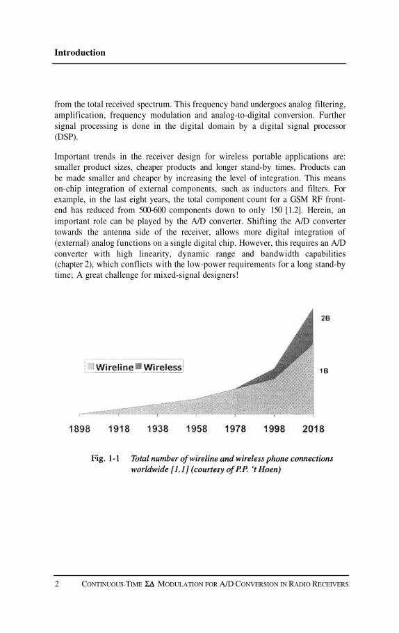
In today’s world, the market for information and communication technology isexpanding as never before. In the last century, the communication market grewfrom zero to about 1 billion telephone connections worldwide [1.1]. It is to beexpected that this amount will double in the next twenty years (Fig. 1-1). Notsurprisingly, wireless communication has become more and more important.Nowadays, in a modern luxury car, besides a radio, one can also find a cellularphone, fax, GPS receiver, television or even an internet browser. All theseportable wireless communication systems have receivers to retrieve theinformation signals from the outside world. The signals are received by anantenna, and the desired signal band, for example a GSM channel, is selected
CONTINUOUS-TIME MODULATION FOR A/D CONVERSION IN RADIO RECEIVERS 1
1
Introduction
from the total received spectrum. This frequency band undergoes analog filtering,amplification, frequency modulation and analog-to-digital conversion. Furthersignal processing is done in the digital domain by a digital signal processor(DSP).
Important trends in the receiver design for wireless portable applications are:smaller product sizes, cheaper products and longer stand-by times. Products canbe made smaller and cheaper by increasing the level of integration. This meanson-chip integration of external components, such as inductors and filters. Forexample, in the last eight years, the total component count for a GSM RF front-end has reduced from 500-600 components down to only 150 [1.2]. Herein, animportant role can be played by the A/D converter. Shifting the A/D convertertowards the antenna side of the receiver, allows more digital integration of(external) analog functions on a single digital chip. However, this requires an A/Dconverter with high linearity, dynamic range and bandwidth capabilities(chapter 2), which conflicts with the low-power requirements for a long stand-bytime; A great challenge for mixed-signal designers!
2 CONTINUOUS-TIME MODULATION FOR A/D CONVERSION IN RADIO RECEIVERS

1.2 Sigma-delta A/D conversion
1.2 Sigma-delta A/D conversion
Signals that are progressing continuously in time and amplitude are classified asanalog signals. An analog-to-digital converter produces a digital representation ofthe analog input signal by sampling the input signal at discrete time moments andquantizing the amplitude of the input signal in discrete amplitude levels. Due tothe finite number of quantization levels, the quantization process causes errors,which set the maximum achievable resolution. The resolution of the ADC can beimproved by increasing the number of quantization levels. In a sigma-deltamodulator, additional techniques are used to achieve higher accuracy, namelyoversampling and noise-shaping. Oversampling means that sampling of theanalog input signal is done with a sampling rate higher than the minimumrequired Nyquist frequency, which is twice the signal bandwidth. Accordingly,the oversampling ratio (OSR) is defined as
where m is the oversampling ratio, is the sampling rate and is the signalbandwidth. Noise-shaping implies filtering of the quantization errors, in order toshape their frequency response. As a result, the quantization error power isreduced in the frequency band of interest, while it is increased outside that band.This way, high resolution can be obtained in a relatively small bandwidth. Thegeneral model of a single-loop sigma-delta modulator is shown in Fig. 1-2a [1.3].Basically, a sigma-delta modulator consists of a loopfilter, performing the noise-shaping, a low resolution quantizer, which is oversampled, and a feedback loop.The loopfilter can be a lowpass or bandpass filter. A first-order lowpass filter is anaccumulator in the discrete-time domain or an integrator in the continuous-timedomain. The quantizer can be modeled as a summation node for the loopfilteroutput signal and the quantization error (Fig. 1-2b).
CONTINUOUS-TIME MODULATION FOR A/D CONVERSION IN RADIO RECEIVERS 3
Introduction
The delay cell with the positive feedback path is the mathematical model of anaccumulator. The output Y of the sigma-delta modulator of Fig. 1-2b is equal to
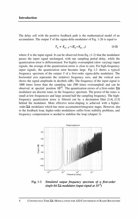
where X is the input signal. It can be observed from Eq. (1-2) that the modulatorpasses the input signal unchanged, with one sampling period delay, while thequantization error is differentiated. For highly oversampled (slow varying) inputsignals, the average of the quantization errors is close to zero. For high-frequencyinput signals, the quantization error becomes large. Fig. 1-3 shows a typicalfrequency spectrum of the output Y of a first-order sigma-delta modulator. Thehorizontal axis represents the (relative) frequency axis, and the vertical axisshows the signal amplitude in decibels (dB). The frequency of the input signal is1000 times lower than the sampling rate (500 times oversampled) and can beobserved at spectral position The quantization errors of a first-ordermodulator are discrete tones in the frequency spectrum. The power of the tones issmall at low frequencies and large around half the sampling frequency. The high-frequency quantization noise is filtered out by a decimation filter [1.4], [1.5]behind the modulator. More effective noise-shaping is achieved with a higher-order modulator which has more accumulator/integrator stages. However, dueto the feedback loop, higher-order modulators suffer from stability problems, andfrequency compensation is needed to stabilize the loop (chapter 3).
4 CONTINUOUS-TIME MODULATION FOR A/D CONVERSION IN RADIO RECEIVERS
1.3 System level simulation
1.3 System level simulation
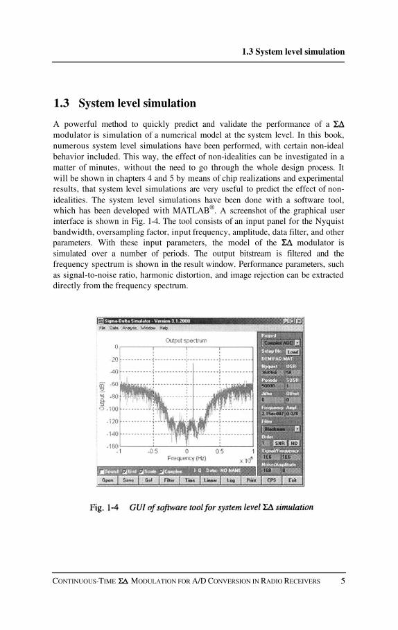
A powerful method to quickly predict and validate the performance of amodulator is simulation of a numerical model at the system level. In this book,numerous system level simulations have been performed, with certain non-idealbehavior included. This way, the effect of non-idealities can be investigated in amatter of minutes, without the need to go through the whole design process. Itwill be shown in chapters 4 and 5 by means of chip realizations and experimentalresults, that system level simulations are very useful to predict the effect of non-idealities. The system level simulations have been done with a software tool,which has been developed with MATLAB®. A screenshot of the graphical userinterface is shown in Fig. 1-4. The tool consists of an input panel for the Nyquistbandwidth, oversampling factor, input frequency, amplitude, data filter, and otherparameters. With these input parameters, the model of the modulator issimulated over a number of periods. The output bitstream is filtered and thefrequency spectrum is shown in the result window. Performance parameters, suchas signal-to-noise ratio, harmonic distortion, and image rejection can be extracteddirectly from the frequency spectrum.
CONTINUOUS-TIME MODULATION FOR A/D CONVERSION IN RADIO RECEIVERS 5

Introduction
1.4 Motivation and objectives
The main practical motivation for the work in this book, is the demand for high-performance and low-power A/D converters in receivers. With a highperformance A/D converter, the level of integration of a receiver can be increased,for example by means of digital filters. Increasing the level of integration reducescomponent count, cost, and product size. This implies higher demands on theADC concerning linearity, dynamic range, input frequency and bandwidth. In thisbook three main subjects have been investigated which are
linearity
power consumption
image rejection performance
Low-power consumption is an important issue in battery-powered applications,like mobile phones. Improving the performance, while reducing the total power,requires new design topologies and innovative solutions. This is an importantscientific motivation for exploring the relations between power and performance.In this work, the total power consumption is optimized at three levels in the top-down design process:
system architecture level
functional block level
circuit level
This book describes the results of these three design steps. First, the place of theADC in the total system architecture is analyzed, which has a strong relation withthe required performance. Secondly, the power is reduced by combining differentfunctional blocks (mixer, filter and ADC) and the power-to-performance relationsare analyzed. The last objective is the design of prototype test chips to show thathigh performance can be realized at low-power consumption.
1.5 Organization of the work
In this book the theory and design of continuous-time modulators for A/Dconversion in radio receivers is described. In chapter 2, it will be shown that therequired performance of the ADC depends very much on its place in the receiver.Single-bit continuous-time modulation is a good technique for A/Dconversion in receivers, as it incorporates inherent anti-aliasing filtering, excellent
6 CONTINUOUS-TIME MODULATION FOR A/D CONVERSION IN RADIO RECEIVERS

1.5 Organization of the work
linearity performance, and low-power capability. All these performance aspectsare particularly important in battery-powered receivers. The main performanceparameters are described and a figure-of-merit is presented that can be used forcomparison between different designs. Moreover, A/D converter specificationsfor GSM mobile phone and AM/FM radio are presented, which are the mainapplications of this work.
In chapter 3, the theory of higher-order continuous-time modulation isdescribed. Important aspects, determining the performance of a continuous-time
modulator, are quantization noise, DC tones, intersymbol interference, clockjitter, and aliasing. The design of higher-order filters is described, withButterworth and inverse-Chebyshev filter characteristics. With the availability ofquadrature signals in a radio receiver, the theory of quadrature modulation istreated as well.
Chapter 4 presents the theory, design, and realization of a continuous-timemodulator with integrated mixer for A/D conversion of IF signals. The workfocuses on high linearity performance and low-power consumption of themodulator. Theoretical results and measured performance of the prototype chipsare analysed.
The design of a quadrature modulator can be found in chapter 5. Themodulator consists of two IF modulators as presented in chapter 4. The focusof this work is the image rejection performance. To improve image rejectionperformance, a novel dynamic element matching algorithm is presented, which isbased on the complex output data of the quadrature modulator. Carefulimplementation of the dynamic element matching circuit is required, as themodulator is very sensitive to parasitic non-idealities.
In chapter 6, the main conclusions are summarized. The performance of theprototype test chips that have been described in this book are compared with otherstate-of-the-art test designs from literature.
CONTINUOUS-TIME MODULATION FOR A/D CONVERSION IN RADIO RECEIVERS 7
Introduction
References
[1.1]
[1.2]
[1.3]
[1.4]
[1.5]
Hoen, P.P. ‘t, “Telecommunicatie: een wereldmarkt,” Tijdschrift vanhet nederlands elektronica- en radiogenootschap, no. 3, pp. 117-124, 1999.Fenk, J. “Highly integrated RF-IC’s for GSM, DECT and UMTSsystems,” Proc. of ESSCIRC, pp. 11-14, Sept. 1999.Norsworthy, S.R., R. Schreier, G.C. Temes, Delta-sigma dataconverters - Theory, design, and simulation, IEEE Press, New York,1997.Candy, J.C.,“Decimation for sigma delta modulation,” IEEE Trans.Commun., vol. COM-34, pp. 72-76, Jan. 1986.Park, S., “Multistage decimation filter design techniques for high-resolution sigma-delta A/D converters,” IEEE Trans. Instr.Measurement, vol. 41, pp. 868-873, Dec. 1992.
8 CONTINUOUS-TIME MODULATION FOR A/D CONVERSION IN RADIO RECEIVERS

A/D conversion inradio receivers
2
2.1 Introduction
The main function of a radio receiver is the reception of a, possibly weak, desiredchannel from a wideband frequency spectrum containing strong interferencesignals, with a minimum specified signal-to-noise-and-distortion ratio. Toaccomplish these tasks of selectivity and sensitivity, filters and amplifiers areneeded to suppress interference signals and to increase the desired channel powerrespectively. In general, the analog building blocks determine the sensitivity ofthe receiver and the filters determine the selectivity. Because the desired channelband may be modulated at a high frequency (GSM channels near 1 GHz), mixersare also used to translate the channel to more appropriate lower frequencies. Theanalog-to-digital converter is becoming an important part of the receiverarchitecture. The place of the ADC determines which functions are implementedwith analog circuitry and what functionality is done in the digital signalprocessor. As the size of digital circuits as well as the supply voltage (and power)decreases with each new technology generation, putting more functionality intothe digital signal processor (DSP) is required to take advantage of these trends.Moreover, analog signal processing functionality such as filtering and frequencytranslation, can be performed by the DSP with almost any degree of perfectionrequired. In this chapter, the place of the ADC in the receiver architecture isdiscussed in section 2.2. In section 2.3 motivations are given for using a
CONTINUOUS-TIME MODULATION FOR A/D CONVERSION IN RADIO RECEIVERS 9

A/D conversion in radio receivers
modulator as A/D converter in a receiver. Shifting part of the selectivity into theDSP requires an ADC with a large dynamic range and high linearity. These andother performance parameters are described in section 2.4. In section 2.5 someimportant issues concerning GSM mobile phone, and AM/FM radiospecifications are highlighted, which are the applications of the work in this book.The conclusions of this chapter are summarized in section 2.6.
2.2
Basically, the architecture of a radio receiver front-end consists of an antenna, ananalog signal processing part, an A/D converter, and a digital signal processor(Fig. 2-1). The place of the A/D converter in a receiver front-end is of greatimportance as it affects overall performance, complexity, power consumption,and cost. In today’s commercial receivers, the analog part includes an RF Bipolarchip e.g. for the low-noise amplifier (LNA) [2.1] and external filters, inductors,capacitors, etc. The digital part includes a single digital CMOS chip. The analogpart significantly adds to the total component count which has a substantialimpact on size and cost.
Shifting analog functions such as filters, mixers and amplifiers into the digitaldomain or, in other words, moving the A/D converter towards the antenna,reduces the complexity of the receiver. However, as the A/D converter movescloser to the antenna side, the required performance specifications for the ADCbecome very stringent. In section 2.2.1, the traditional superheterodyne receiverwith baseband A/D conversion is shown. Moving the A/D converter to the
10 CONTINUOUS-TIME MODULATION FOR A/D CONVERSION IN RADIO RECEIVERS
From baseband to RF A/D conversion

2.2 From baseband to RF A/D conversion
antenna side finally results in the ultimate digital receiver (section 2.2.3), howeverwith (yet) impossible ADC specifications.
2.2.1 Heterodyne receiver with baseband A/D conversion
The model of a traditional superheterodyne receiver architecture is shown inFig. 2-2. The antenna signal is filtered by a wideband bandpass filter andamplified by a low-noise amplifier. The desired channel, modulated at a radiofrequency (RF), is mixed down to a lower intermediate frequency (IF), which forexample is 10.7 MHz in FM radio applications [2.2]. External narrowbandchannel filters with high selectivity, such as ceramic filters or SAW filters, areavailable at this IF. The first local oscillator (LO) frequency is tuned toselect the desired RF channel. Before frequency translation, an image rejection(IR) filter reduces signal power at the image frequency. The channel filter passesthe desired IF channel, and suppresses adjacent channels by about 30-40 dB. Avariable gain amplifier with automatic gain control (AGC) fits the signal powerinto the dynamic input range of the subsequent blocks. Two IF mixer stages,driven by quadrature local oscillator signals convert the IFchannel to DC or a low frequency. Quadrature mixing of the signal to in-phase (I)and quadrature-phase (Q) channels is required to achieve a sufficient amount ofimage suppression (section 2.4.3). After quadrature mixing, the I and Q channelsat baseband are filtered by lowpass anti-aliasing filters (section 3.2.6) anddigitized. Further signal processing is done in the DSP. Requirements for the A/Dconverters in the superheterodyne receiver regarding dynamic range, linearity,and bandwidth are relaxed because of all the filters, in particular the channel filter,preceding the A/D converters.
CONTINUOUS-TIME MODULATION FOR A/D CONVERSION IN RADIO RECEIVERS 11

A/D conversion in radio receivers
In addition, the baseband channel can be digitized at a relatively low sample rate.Therefore, power efficiency of the ADCs is high [2.3]. Image rejectionrequirements strongly depend on the choice of the second IF frequency of thequadrature signals. If the quadrature channel is translated to a low frequency(low-IF downconversion), the image signal and desired channel are not related,and the image signal may be stronger than the desired channel (Fig.2-3a).Therefore, image rejection has to be large and for example in the order of 80-90 dB for FM radio. The channel filter suppresses the image signal with 40 dBand another 40 dB of rejection must come from the quadrature mixing.
The main advantage of low-IF downconversion is that offset as well as flickernoise do not interfere with the desired signal. This is not the case if zero-IFdownconversion is performed (Fig. 2-3b). As the desired channel is mixed downto DC, offset and flicker noise are present in the middle of the signal band andinterfere with the signal. However, in case of zero-IF downconversion, the imageand the desired signal are the same. The quadrature signals are used to reconstructthe original upper and lower modulation sidebands. The required accuracy of thequadrature signals depends on the modulation technique which is used. Forexample, a 1 dB amplitude imbalance and 5-degree phase imbalance areacceptable for a QPSK-OFDM-QAM system [2.4].
12 CONTINUOUS-TIME MODULATION FOR A/D CONVERSION IN RADIO RECEIVERS

2.2 From baseband to RF A/D conversion
2.2.2 Heterodyne receiver with IF digitizing
An alternative receiver architecture, which is growing more popular, is theheterodyne receiver with IF A/D conversion (Fig. 2-4). The ADC is shifted infront of the IF mixers and quadrature modulation is performed by the DSP, withlow-power consumption and perfect linearity and matching for excellent imagerejection performance. Moreover, an IF A/D converter is insensitive to DC offsetand low-frequency noise. As quadrature mixing is done in the digital domain,only one ADC is required. The channel filter in front preserves the moderatedynamic range, bandwidth, and linearity requirements for the ADC. A drawbackis that the sample rate of the ADC is at least twice the IF of the input channel.Furthermore, linearity and dynamic range requirements are more difficult to meetat higher frequencies due to circuit non-idealities and parasitic effects. Theseconstraints make the ADC for IF digitizing much less power efficient, especiallyif the IF is high, compared to a baseband ADC. In [2.5] - [2.9], numerous designsare proposed for bandpass A/D conversion in radio receivers.
The next step is to shift the A/D converter in front of the channel selection filter(Fig. 2-5) [2.10]. A wideband ADC digitizes all channels and channel selection isimplemented in the DSP. This is especially advantageous in a base station forcellular phones, where only one receiver board is required with this architecturefor processing all channels. In this case a higher power consumption can beallowed. Another aspect of this architecture is the flexibility in adapting to systemchanges, by only changing software programs [2.11]. However, the lack of analogprefiltering by a channel filter and amplification by a VGA puts heavy linearityand dynamic range requirements onto the ADC.
CONTINUOUS-TIME MODULATION FOR A/D CONVERSION IN RADIO RECEIVERS 13

A/D conversion in radio receivers
2.2.3 Receiver architecture with RF digitizing
The ultimate digital receiver architecture is shown in Fig. 2-6. The A/D converteris only preceded by an RF bandpass filter and an LNA, which may have someAGC. Signal processing such as frequency translation, channel filtering, andsignal demodulation is done all in one digital chip. Requirements for the A/Dconverter in this architecture are extremely heavy, as it has to handle the fullantenna receiving power. This means the converter should have high dynamicrange, high linearity, large bandwidth at high (RF) frequencies. If it were possibleto design, the ADC in this architecture would most likely consume an excessiveamount of power. Yet, attempts have been made to explore the boundaries of RFA/D conversion [2.12], [2.13].
2.3 Sigma-delta modulation in a heterodyne receiver
It was explained in section 2.2.1 that the ADCs in the traditional heterodynereceiver architecture have relaxed requirements, as the desired channel is alreadyselected and converted to baseband. In [2.14] - [2.17] it is shown that high
14 CONTINUOUS-TIME MODULATION FOR A/D CONVERSION IN RADIO RECEIVERS

2.3 Sigma-delta modulation in a heterodyne receiver
performance and low-power A/D converters, based on the principle ofmodulation, are available for baseband signal conversion. modulation is awidely used technique for high-performance and low-power A/D conversion ofrelatively low-bandwidth signals. Numerous designs have been presented foraudio and radio applications [2.5] - [2.9], [2.14] - [2.17]. In particular, lowpasscontinuous-time modulation is suitable for application in the receiverarchitecture of Fig. 2-2, due to its low-power capability, high linearity andinherent anti-aliasing filtering (shown in the upper quadrature path inFig.2-7) [2.3]. These issues are discussed in detail in chapter 3. It was shown inthe previous sections that digital integration of filters and mixers, in respect to atraditional receiver with baseband A/D converters, results in tough linearity,dynamic range, and bandwidth requirements. In addition, these requirements aremuch more difficult to meet at intermediate frequencies, let alone radiofrequencies. Hence, digital integration of the second IF analog mixers(section 2.2.2) would require a more difficult and less optimal A/D converter interms of performance and power consumption.
In this book a technique is investigated to integrate the IF mixer with a lowpassmodulator in the analog domain (chapter 4). This mixer and modulator
topology will be referred to as IF-to-baseband modulator (or IFmodulator). It is shown that the IF modulator (lower path Fig.2-7) provideshighly linear mixing, while power consumption is determined by the low-powerADC only. Moreover, two IF modulators in a quadrature configuration can bedynamically matched to improve image rejection performance (chapter 5). Thedynamic element matching (DEM) algorithm is based on the complex bitstream
CONTINUOUS-TIME MODULATION FOR A/D CONVERSION IN RADIO RECEIVERS 15

A/D conversion in radio receivers
output of the quadrature modulator (Fig. 2-8). The result is a low-powersystem with high image rejection.
2.4 Performance parameters
In the previous section, the most important specifications for A/D convertersembedded in a receiver architecture have been distinguished. These are dynamicrange, linearity, image rejection, and power consumption. It was shown that thespecifications strongly depend on the place of the A/D converter in the receiver. Inthis section, the ADC performance parameters are explained. In the final section,a figure-of-merit is defined, based on these parameters, for an objectivecomparison between different A/D converters.
2.4.1 Dynamic range
One of the important performance parameters of an A/D converter is dynamicrange. In literature a number of different terms occur, indicating dynamic rangeperformance, with only minor differences. The main definitions which are usedthroughout this book have been listed below. These are dynamic range, signal-to-noise ratio, peak SNR and resolution.
Dynamic range (DR) - ratio between maximum signal power and minimumdetectable signal power within a specified bandwidth.
Signal-to-noise ratio (SNR) - ratio between signal power and noise power withina certain bandwidth.
16 CONTINUOUS-TIME MODULATION FOR A/D CONVERSION IN RADIO RECEIVERS

2.4 Performance parameters
Peak SNR - ratio between maximum signal power and noise power within acertain bandwidth.
Resolution - smallest output step, or least significant bit (LSB), indicating achange of the input signal.
It should be noted that these performance parameters are all relative numbers.Information about the (maximum) input power is needed for a completequalification.
2.4.2 Linearity
A parameter which is particularly important in receivers is linearity. Non-linearityintroduces distortion components, which should be weaker than the minimumdetectable signal power. Different definitions, specifying non-linearity of thesystem, are distinguished. These are harmonic distortion, spurious-free dynamicrange, intermodulation distortion, intermodulation intercept point, cross-modulation distortion and signal-to-noise-and-distortion ratio.
Harmonic distortion (HDx) - ratio between signal power and power of distortioncomponent at harmonic of signal frequency. Commonly, the second and thirdharmonic components, which are indicated as HD2 and HD3 respectively, are themost important (Fig.2-9a).
Spurious-free dynamic range (SFDR) - ratio between maximum signal carrierand the maximum (in-band) distortion component (Fig.2-9b).
Intermodulation distortion (IMx) - modulation of multiple signal tones, due tonon-linearity, to spectral positions which are combinations of the signalfrequencies. Fig. 2-9c shows a frequency spectrum with two signal tones at and
respectively. Due to second-order and third-order distortion, intermodulationtones occur at spectral positions and (andrespectively. Intermodulation distortion is defined as the distance between thecarrier power of a signal tone and the power of the specifiedintermodulation distortion tone. Again, the second-order and third-orderintermodulation tones, which are denned by IM2 and IM3 respectively, areusually the most important.
Intermodulation intercept point (IPx) - (theoretical) signal carrier power forwhich the power of the specified intermodulation distortion tone is equalto the signal carrier power (or in other words, the signal power for which IMx is0dB). Again, IP2 and IP3 are the most important.
CONTINUOUS-TIME MODULATION FOR A/D CONVERSION IN RADIO RECEIVERS 17

A/D conversion in radio receivers
Cross-modulation distortion (CM) - modulation of spectral content around thecarrier of an interference channel (right side of Fig.2-9d), due to non-linearity, inthe desired signal band (left side of Fig.2-9d). Cross-modulation distortion isindicated as the distance between the signal carrier power and the cross-modulation distortion components.
Signal-to-noise-and-distortion ratio (SNDR) - ratio between signal power andtotal noise and distortion power within a certain bandwidth.
18 CONTINUOUS-TIME MODULATION FOR A/D CONVERSION IN RADIO RECEIVERS
2.4 Performance parameters
2.4.3 Image rejection
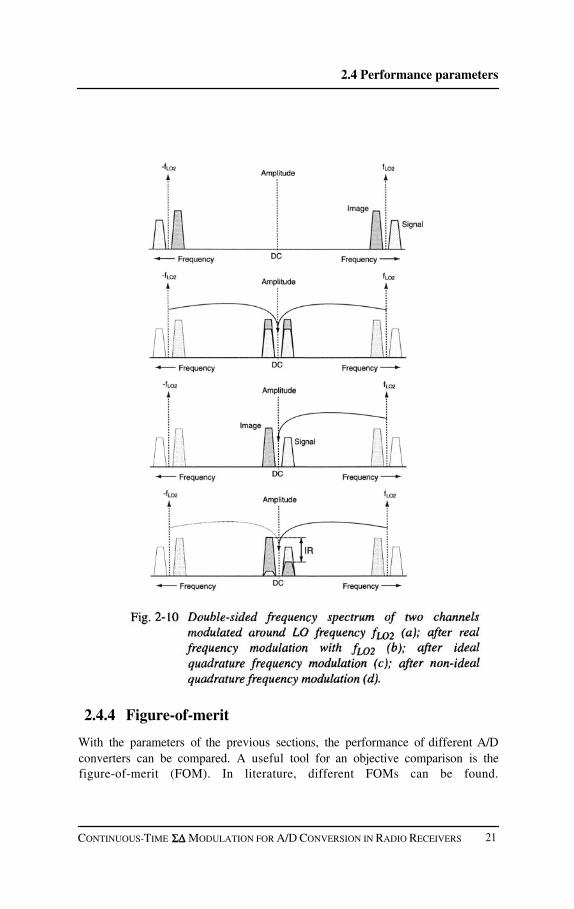
Frequency translation in a receiver, by means of a frequency multiplier or mixer,introduces the problem of image interference. Fig.2-10a shows the positive andnegative frequency spectrum of two channels modulated around a frequencyThe light colored channel at the right of is considered to be the desiredsignal, and the dark colored channel at the left of is referred to as the image.When applied to a single mixer, operating at frequency both channels areupconverted and downconverted. The downconverted tones occur around DC. Asingle (or real) mixer is equally sensitive to signals at both sides of the LO carrier.In other words, the result of real frequency translation is a compound signal band,containing the spectral contents of both channels around (Fig.2-10b). If thedesired and image signals represent two different radio channels, a mixture ofboth channels would be audible after frequency translation. To handle thisproblem, which is known as image interference, the technique of quadraturemixing is used.
In the complex domain, a sinusoidal signal can be represented by the sum of apositive and a negative frequency component according to
where j is the complex operator, is the frequency (rad/s) and the phase (rad).It becomes clear from Eq. (2-1) that the positive and negative frequency terms of acosine have equal phases, while the frequency terms of a sine are 180° out ofphase. Moreover, comparing both signals shows that the phase differencesbetween the positive and negative frequency terms of the cosine and sine signalsare 270° and 90° respectively. This difference in phases is used to select either thepositive or negative frequency component of a sinusoidal signal through complexadding or subtracting. This is shown mathematically by the following relations
Consider the positive frequency term being the desired signal and the negativeterm as the image. By complex adding of quadrature signals, according toEq. (2-2), the desired signal (positive frequency) is selected while the image(negative frequency) is cancelled out. Complete cancellation of the image occursif the quadrature signals have
CONTINUOUS-TIME MODULATION FOR A/D CONVERSION IN RADIO RECEIVERS 19
A/D conversion in radio receivers
equal gains
exactly 90° phase difference
If the signals in Fig.2-10a are mixed by two identical mixers with 90° phasedifference, quadrature signals are available at the output of the mixers. Thisimplies that the desired signal can be distinguished from the image signal bycomplex adding of the quadrature mixer outputs. Fig.2-10c shows the complexfrequency spectrum of the signals of Fig.2-10a after quadrature demodulation. Inthe positive frequency plane the desired signal band is present, while the imageonly appears in the negative frequency plane.
Due to mismatch, quadrature signals which are generated in the analog domain donot exactly meet the gain and phase requirements. Taking into account a relativegain error and a phase error Eq. (2-2) changes to
for small error values. Eq. (2-3) shows that a suppressed image term is present.The distance between the power of the image in the negative plane and the‘leaked’ image in the positive frequency plane is called the image rejection (IR)
Example 2.1: In the case of a phase error of 1° and a gain error of 1% theimage rejection is 40 dB, which means that the image signal is 40 dB lowerthan the carrier of the desired signal.
Fig.2-10d shows the complex spectrum of the signals of Fig.2-10a afterquadrature frequency translation with a phase and gain error between thequadrature signals. The distance between the power of the image signal in thenegative frequency plane, and the power of the image leakage in the positivefrequency plane is the image rejection. For a state-of-the-art technology, typicalimage rejection ratios of about 45-50 dB can be achieved, based on matching. Formany applications, this amount of image rejection is not sufficient. Othertechniques can be used to further reduce image interference. The channel filter(Fig.2-2) already suppresses the image signal by 40 dB. Moreover, active orpassive image rejection filters[2.18],[2.19], double quadraturemixers [2.20], [2.21], and dynamic element matching (chapter 5) effectivelyimprove image rejection.
20 CONTINUOUS-TIME MODULATION FOR A/D CONVERSION IN RADIO RECEIVERS
2.4 Performance parameters
CONTINUOUS-TIME MODULATION FOR A/D CONVERSION IN RADIO RECEIVERS
2.4.4 Figure-of-merit
With the parameters of the previous sections, the performance of different A/Dconverters can be compared. A useful tool for an objective comparison is thefigure-of-merit (FOM). In literature, different FOMs can be found.
21

A/D conversion in radio receivers
In [2.17], [2.22] an FOM is presented, expressing the power efficiency of an A/Dconverter in relation to the dynamic range (power) in a certain bandwidth
where T is temperature (K), k is Boltzman’s constant (J/K), BW is the bandwidth(Hz) and P the power consumption (W) of the ADC. The FOM of Eq. (2-5) isequal to 1 for an integrator, implemented by an ideal class B amplifier [2.17]. ThisFOM does not contain linearity performance of the ADC, which is important forADCs in receivers. Another FOM, which does include distortion, is related to theSNDR rather than DR
Because of the inclusion of distortion, the SNDR is always equal to or lower thanthe DR performance. Therefore, the FOM of Eq. (2-6) gives a lower value than theFOM of Eq. (2-5). With a FOM, only a rough comparison is made betweendifferent implementations. Other parameters, such as maximum input power,supply voltage or chip area, have not been taken into account and may be evenlyimportant for particular applications. In chapter 6, different ADC designs fromliterature have been compared with the designs in this book, using the FOM ofEq. (2-6).
Example 2.2: Consider the following data: SNDR is 90 dB BW isand P is Substituting this data in Eq. (2-6) gives a
FOM of
2.5 GSM and AM/FM radio specifications
In Europe, the GSM transmit channels from a base cell station are modulated inthe 935-960 MHz band, containing 125 channels of 200 kHz bandwidth. Themodulation technique is Gaussian minimum-shift-keying (GMSK) with a datarate of 270.833 Kbits/sec. The minimum power of a desired channel at theantenna of the receiver is specified to be -104 dBm. To have sufficiently low biterror rate (BER), 9 dB of SNDR is required. This implies that the power of totalin-band noise and distortion should be as low as -113 dBm. Total power of theadjacent interference channels in the GSM band can be up to -23 dBm, resulting
22 CONTINUOUS-TIME MODULATION FOR A/D CONVERSION IN RADIO RECEIVERS
2.5 GSM and AM/FM radio specifications
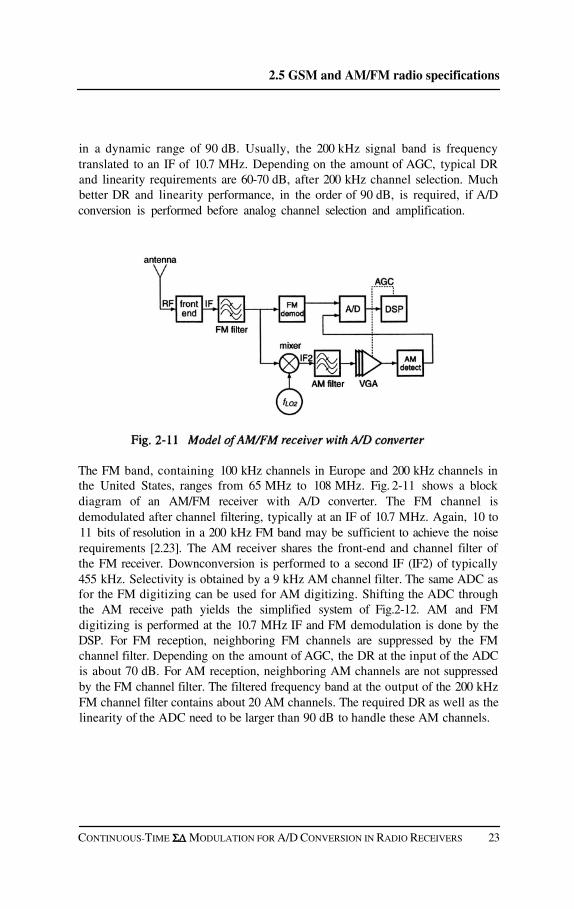
in a dynamic range of 90 dB. Usually, the 200 kHz signal band is frequencytranslated to an IF of 10.7 MHz. Depending on the amount of AGC, typical DRand linearity requirements are 60-70 dB, after 200 kHz channel selection. Muchbetter DR and linearity performance, in the order of 90 dB, is required, if A/Dconversion is performed before analog channel selection and amplification.
The FM band, containing 100 kHz channels in Europe and 200 kHz channels inthe United States, ranges from 65 MHz to 108 MHz. Fig. 2-11 shows a blockdiagram of an AM/FM receiver with A/D converter. The FM channel isdemodulated after channel filtering, typically at an IF of 10.7 MHz. Again, 10 to11 bits of resolution in a 200 kHz FM band may be sufficient to achieve the noiserequirements [2.23]. The AM receiver shares the front-end and channel filter ofthe FM receiver. Downconversion is performed to a second IF (IF2) of typically455 kHz. Selectivity is obtained by a 9 kHz AM channel filter. The same ADC asfor the FM digitizing can be used for AM digitizing. Shifting the ADC throughthe AM receive path yields the simplified system of Fig.2-12. AM and FMdigitizing is performed at the 10.7 MHz IF and FM demodulation is done by theDSP. For FM reception, neighboring FM channels are suppressed by the FMchannel filter. Depending on the amount of AGC, the DR at the input of the ADCis about 70 dB. For AM reception, neighboring AM channels are not suppressedby the FM channel filter. The filtered frequency band at the output of the 200 kHzFM channel filter contains about 20 AM channels. The required DR as well as thelinearity of the ADC need to be larger than 90 dB to handle these AM channels.
CONTINUOUS-TIME MODULATION FOR A/D CONVERSION IN RADIO RECEIVERS 23

A/D conversion in radio receivers
Some of the key issues in this book are dynamic range and linearity of the ADC.Increasing the performance of the ADC may result in relaxed requirements for thechannel filter in the receiver path and a higher degree of integration. However, acheaper channel filter with a low quality factor provides less filtering of directneighboring channels. Therefore, suppression of the image channel, in the case oflow-IF receivers, is also less effective. This implies that the image rejectionrequirement for the ADCs in a quadrature configuration becomes more stringentas well.
2.6 Summary
In this chapter some important performance parameters for the A/D converter in aradio receiver have been described. It was shown that the performancerequirements strongly depend on the place of the A/D converter in the receiver.For reasons of cost, size and complexity reduction, an important trend in receiverdesign is digital integration of analog functionality, such as mixers and filters.Shifting the A/D converter towards the antenna side of the receiver results intough requirements regarding dynamic range and linearity. These requirementsare more difficult to meet at higher frequencies, due to circuit non-idealities andparasitic effects.
Baseband A/D converters in the traditional heterodyne receiver of Fig.2-2 havethe most relaxed requirements. This is because interference signals have beenfiltered out by the channel filter and the desired channel is modulated down to DCor a low-IF frequency. At DC or a low-IF frequency, high linearity performance isachieved easily, as the low frequency (DC) gain of an amplifier can be high.Therefore, for high performance and low-power consumption of the A/Dconverter, the heterodyne receiver architecture of Fig. 2-2 with the analog mixersshould be preserved.
24 CONTINUOUS-TIME MODULATION FOR A/D CONVERSION IN RADIO RECEIVERS

2.6 Summary
Digital integration of the channel filter in GSM or radio receivers puts heavylinearity (and image rejection) requirements on the VGA, quadrature mixers, anti-aliasing filters and A/D converters. A single-bit continuous-time basebandmodulator has the ability of performing highly linear A/D conversion. Moreover,as sampling is done after filtering of the input signal by the continuous-timeloopfilter, it has an inherent anti-aliasing filter. In this book, the combined designof a mixer and continuous-time modulator is investigated for highperformance IF-to-baseband A/D conversion (chapter 4). With this A/Dconverter, channel filter requirements can be relaxed. Besides linearity anddynamic range, high image rejection performance is required as well. Inchapter 5, the image rejection performance of the IF-to-baseband modulatorin a quadrature configuration is investigated.
CONTINUOUS-TIME MODULATION FOR A/D CONVERSION IN RADIO RECEIVERS 25

A/D conversion in radio receivers
References
[2.1] Sevenhans, J., “The Single-Chip Digital Mobile Radio: Does itReally Make Sense?,” ISSCC Dig. Tech. Papers, pp. 122-123, Feb.1999.
[2.2] Kianush, K., C. Vaucher, “A global car radio IC with inaudiblesignal quality checks,” ISSCC Dig. Tech. Papers, pp. 130-131, Feb.1998.
[2.3] Breems, L.J., E.J. van der Zwan and J.H. Huijsing, “A 1.8mWCMOS Modulator for Mobile Communication,” Proc. ofWorkshop on Circuits, Systems and Signal Processing, pp. 61-64,Nov. 1998.
[2.4]
[2.5]
Liu, Chia-Liang, “Impacts of I/Q imbalance on QPSK-OFDM-QAM detection,” Proc. of Int. Conf. on Consumer Electronics, pp.384-385, July, 1998.Jantzi, S.A., K.W. Martin, and A.S. Sedra, “Quadrature Bandpass
Modulation for Digital Radio,” IEEE J. Solid-State Circuits, vol.32, pp. 1935-1950, Dec. 1997.
[2.6] Singor, F.W., W.M. Snelgrove, “Switched-Capacitor BandpassDelta-Sigma A/D Modulation at 10.7 MHz,” IEEE J. Solid-StateCircuits, vol. 30, pp. 184-192, March 1995.
[2.7] Song, B.S., “A Fourth-Order Bandpass Delta-Sigma Modulator withReduced Number of Op Amps,” IEEE J. Solid-State Circuits, vol.30, pp. 1309-1315, Dec. 1995.Ong A.K., B.A. Wooley, “A Two-Path Bandpass Modulator forDigital IF Extraction at 20 MHz,” IEEE J. Solid-State Circuits, vol.32, pp. 1920-1934, Dec. 1997.
[2.8]
Hairapetian, A., “An 81 MHz IF Receiver in CMOS,” ISSCC Dig.Tech. Papers, pp. 56-57, Feb. 1996.
[2.9]
[2.10]Vorenkamp, P., R. Roovers, “A 12-b, 60-MSample/s CascadedFolding and Interpolating ADC,” IEEE J. Solid-State Circuits, vol.32, pp. 1876-1886, Dec. 1997.Kwak, S-U, B-S. Song, K. Bacrania, “A 15-b, 5-Msample/s Low-Spurious CMOS ADC,” IEEE J. of Solid-State Circuits, vol. 32, pp.1866-1875, Dec. 1997.
[2.11]
Gao, W., W.M. Snelgrove, “A 950-MHz IF Second-Order IntegratedLC Bandpass Delta-Sigma Modulator,” IEEE J. Solid-State Circuits,vol. 33, pp. 723-732, May 1998.
[2.12]
[2.13] Cherry, J.A, W.M. Snelgrove, Continuous-time delta-sigmamodulators for high-speed A/D conversion; theory, practice and
CONTINUOUS-TIME MODULATION FOR A/D CONVERSION IN RADIO RECEIVERS26

2.6 Summary
[2.14]
[2.15]
[2.16]
[2.17]
[2.18]
[2.19]
[2.20]
[2.21]
[2.22]
[2.23]
fundamental performance limits, Kluwer Academic Publishers,Boston, 2000.Fujimori, I., K. Koyama, D. Trager, F. Tam, L. Longo, “A 5-VSingle-Chip Delta-Sigma Audio A/D Converter with 111 dBDynamic Range,” IEEE J. Solid-State Circuits, vol. 32, pp. 329-336,March 1997.Ritoniemi, T., E. Pajarre, S. Ingalsuo, T. Husu, V. Eerola, T.Saramaki, “A Stereo Audio Sigma-Delta A/D-Converter,” IEEE J.Solid-State Circuits, vol. 29, pp. 1514-1523, Dec. 1994.Coban, A.L., P.E. Allen, “A 1.5 V 1.0 mW Audio Modulatorwith 98 dB Dynamic Range,” ISSCC Dig. Tech. Papers, pp. 50-51,Feb. 1999.Rabii, S., B. Wooley, “A 1.8-V digital-audio Sigma-Delta modulatorin 0.8µm CMOS,” IEEE J. Solid-State Circuits, vol. 32, pp. 783-796, June 1997.Voorman, J.O., “Continuous-time analog integrated filters,” inIntegrated Continuous-Time Filters, IEEE Press, New York, 1993.Gingell, M.J., “Single sideband modulation using sequenceasymmetric polyphase networks,” Elect. Commun., vol. 48, pp. 21-25, 1973.Crols, J. M.S.J. Steyaert, “A Single-Chip 900 MHz CMOS ReceiverFront-End with a High Performance Low-IF Topology,” IEEE J.Solid-State Circuits, vol. 30, pp. 1483-1492, Dec. 1995.Rudell, J.C., J.J. Ou, T.B. Cho, G. Chien, F. Brianti, J. A. Weldon,P. R. Gray, “A 1.9-GHz Wide-Band IF Double Conversion CMOSReceiver for Cordless Telephone Applications,” IEEE J. Solid-StateCircuits, vol. 32, pp. 2071-2088, Dec. 1997.Sansen, W., Advanced engineering course on low-voltage low-power analog CMOS design, Lausanne, June 21-25, 1999.Zwan, E.J. van der, K. Philips, C. Bastiaanse, “A 10.7 MHz IF-to-Baseband A/D Conversion System for AM/FM RadioReceivers,” ISSCC Dig. Tech. Papers, pp. 340-341, Feb. 2000.
CONTINUOUS-TIME MODULATION FOR A/D CONVERSION IN RADIO RECEIVERS 27

Continuous-timesigma-deltamodulation
3.1 Introduction
In 1954, a patent was filed by Cutler [3.1] of a feedback system with alow-resolution quantizer in the forward path. The quantization error of a quantizerwas fed back and subtracted from the input signal. This principle of improving theresolution of a coarse quantizer by use of feedback is the basic concept of adelta-sigma or sigma-delta converter [3.2]. In 1962, Inose et al. [3.3] came upwith the idea of adding a filter in the forward path of a delta modulator [3.4], infront of the quantizer. This system was called a ‘delta-sigma modulator’, where‘delta’ refers to the delta-modulator, and ‘sigma’ refers to summation by theintegrator.
In this chapter, the theory and design of a continuous-time sigma-delta modulatoris explored. In section 3.2 the basic theory of sigma-delta modulation isexplained. Stability analysis of a linear model of a continuous-time sigma-deltamodulator is performed in section 3.3 and in section 3.4 the filter design ofhigher-order lowpass filters has been elaborated. Finally, the design of a complexfilter for a quadrature sigma-delta modulator architecture is presented insection 3.5.
CONTINUOUS-TIME MODULATION FOR A/D CONVERSION IN RADIO RECEIVERS 29
3

CONTINUOUS-TIME MODULATION FOR A/D CONVERSION IN RADIO RECEIVERS30
Oversampling
A one-bit quantizer generates a bitstream pattern with output levels ±q/2 , whereq is the quantization step size. The bitstream spectrum contains information aboutthe input signal and a quantization error, which is introduced by the quantizer.
Continuous-time sigma-delta modulation
3.2 Theory of sigma-delta modulation
In this section, the basic theory of modulation is described and the mainnon-idealities which determine the overall performance. The principles ofoversampling and noise-shaping are explained in section 3.2.1. The error of thequantization process is assumed to be white noise for simplicity of theanalysis [3.5]. However, analyzing the quantization spectrum (section 3.2.2)shows that it is far from white, but contains periodic, offset-related sequenceswhich introduce tones in the output spectrum. As noise imposes a limit on theminimum detectable input signal, distortion affects the performance for themaximum input. In section 3.2.3, the effect of distortion due to non-linearity ofthe input stage of the loopfilter is calculated. Intersymbol interference(section 3.2.4) is caused by waveform asymmetry of the feedback pulses andforms another source of non-linearity in continuous-time modulators. Besidesquantization noise and tones, phase jitter of the reference clock also adds noise tothe system, which decreases the maximum obtainable signal-to-noise ratio(section 3.2.5). Finally, the subject of aliasing is discussed in section 3.2.6, as it isof great importance for a modulator when used in a receiver (section 2.2.1).
3.2.1 Oversampling and noise-shaping
The principle of operation of a modulator is explained by the block diagram ofa single-loop modulator (Fig. 3-1). The modulator consists of a loopfilterwhich in its simplest form is an accumulator or integrator. The filter output issampled and quantized by an A/D converter which introduces a quantization errorE. The digital output signal is subtracted from the analog input via a D/Aconverter in the feedback path. The error E due to the quantization process is thedifference between the analog quantizer input signal and the quantized output.Suppression of the quantization error in a modulator is provided by twomechanisms: oversampling of the signal bandwidth and shaping of the noise bythe loopfilter. Because the reduction of the quantization error by thesemechanisms is so effective, a high-resolution digital output is obtained, usingonly a low-resolution quantizer. In the extreme case a one-bit quantizer with twooutput levels is sufficient. In this section, the principles of oversampling andnoise-shaping are briefly introduced.

CONTINUOUS-TIME MODULATION FOR A/D CONVERSION IN RADIO RECEIVERS 31
where is the signal bandwidth. The oversampling ratio m is the ratio betweenthe sampling frequency and the Nyquist bandwidth (twice the signal bandwidth)
3.2 Theory of sigma-delta modulation
For simplicity, the quantization error is assumed to have a white noisespectrum [3.5] and the total power of the quantization error signal equals [3.2]
The power spectral density of the sampled quantization error signal is
where is the sampling frequency. This equation shows the relation between thequantization noise power and sampling frequency. It shows that the higher thesampling frequency, the lower the noise power density. This is the principle ofoversampling. The integrated noise power within a fixed signal bandwidthdecreases if the sampling rate is increased. In mathematical terms, the totalin-band quantization noise power equals

Continuous-time sigma-delta modulation
The dynamic range is defined as the ratio between the in-band noise power andthe maximum power of the input signal. The maximum input power is about afactor of 4 smaller than the quantizer output power [3.6]
Noise-shaping
For low frequency signals, the DAC in the feedback path has a gain ofapproximately 1. Fig. 3-2 shows a highly simplified linear model of acontinuous-time modulator. Using this model, the output Y(s) of themodulator is determined
where X(s) is the analog input signal and H(s) is the loopfilter transfer function.The first term of the right-hand side of Eq. (3-6) is the signal transfer function(STF) and the second term is the noise transfer function (NTF). If H(s) has alowpass filter characteristic with high DC gain, then for low-frequencies thesignal transfer function is close to 1, while the quantization error tends towardzero (NTF is 0). For frequencies close to half the sampling frequency, the inputsignal is filtered and the quantization error becomes large. This shows that thequantization noise density function is not constant over frequency, but has ashaped frequency spectrum. This is the principle of noise-shaping.
In the next section, the quantization error spectrum is described in more detail.Although, the white noise assumption is useful for estimating the in-bandquantization error power, it is shown that the quantization error signal consists ofsignal dependent sequences, with periodic, offset-related tones for small inputsignals.
32 CONTINUOUS-TIME MODULATION FOR A/D CONVERSION IN RADIO RECEIVERS

3.2.2 Tones
3.2 Theory of sigma-delta modulation
Tones are spectral components that are induced by DC offsets, which generateperiodic quantization error sequences. These periodic quantization errors occur asdiscrete peaks in the frequency spectrum with input signal dependent frequencies.The frequencies of tones are calculated by the empirical relation [3.2]
where n is an integer, is the sampling frequency, is the DC offset voltage andis the quantization step size. This phenomenon has been simulated with a
model of a fourth-order 1-bit sigma-delta modulator. Fig. 3-3 shows the simulatedtime domain quantization error signal in the case of an offset of 3 mVand a 12.96 MHz sampling frequency. Fig. 3-3 reveals that the quantization erroris clearly not a random signal but, on the other hand, that periodic sequences arenot easily recognized. The autocorrelation technique offers more insight into thepresence of tones in the time domain signal [3.2]. With (discrete-time)autocorrelation, the interdependence between a fixed quantization error sequenceand a sequence shifted in time by l sample periods is determined as a function ofl.
CONTINUOUS-TIME MODULATION FOR A/D CONVERSION IN RADIO RECEIVERS 33

Continuous-time sigma-delta modulation
34 CONTINUOUS-TIME MODULATION FOR A/D CONVERSION IN RADIO RECEIVERS

3.2 Theory of sigma-delta modulation
Fig. 3-4 shows the autocorrelation of the quantization error waveform of Fig. 3-3.A periodic sequence can be observed with a period time of (41 kHz).Fig. 3-5 shows the low frequency output spectrum of the modulator with theDC input. A tone of -128 dB occurs at 41 kHz and the harmonics are at 82 kHz,123 kHz, and 164kHz (n is 4, 8, 12 and 16). Moreover, Fig.3-5 shows that theenergy of the tones increases with the frequency. This is due to the decrease inloopgain at higher frequencies. Therefore, the strongest tone occurs at the end ofthe signal band. This can be a serious problem if the gain is not sufficient.
A method to manipulate tones is the use of zeros in the NTF characteristic thatcomply with the inverse Chebyshev placement [3.2]. This way, the NTF gain isdistributed equally within the signal band of interest. These inverse Chebyshevzeros can be made by adding local feedback (resonator) paths in the loopfilter.This will be treated in detail in section 3.4.2. Another way of manipulating tonesis applying a dither signal [3.7] to the input, to decorrelate the quantization errors.This is beyond the scope of this book.
So far, only baseband tones have been investigated. However, at high frequencies(near half the sampling frequency) tones are present as well and are very strongdue to the lack of loopgain at those frequencies. The tones are situated at
The high frequency tones can be demodulated into baseband by even-orderharmonic distortion [3.6] or parasitic coupling of a clock signal with a frequencynear half the sampling rate [3.8], [3.9]. In the case of second harmonic distortionthe baseband tones occur at
where and are two high frequency tones. In the case of modulation withhalf the sampling frequency the in-band tone will be at
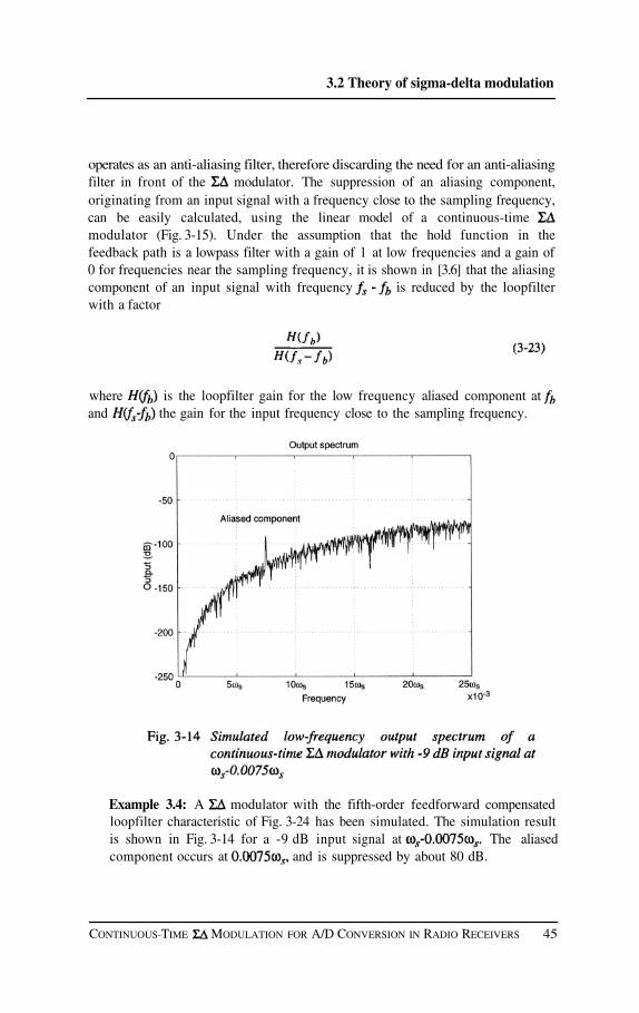
Fig. 3-6 shows the simulated quantization spectrum near half the samplingfrequency for a 3mV DC input. A large tone of -l0dB occurs at 6.4795 MHz,which is located at an offset frequency of 20.5 kHz away from half the samplingfrequency.
CONTINUOUS-TIME MODULATION FOR A/D CONVERSION IN RADIO RECEIVERS 35

Continuous-time sigma-delta modulation
36 CONTINUOUS-TIME MODULATION FOR A/D CONVERSION IN RADIO RECEIVERS

3.2 Theory of sigma-delta modulation
When this tone is modulated with half the sampling frequency, it will bedownconverted to 20.5 kHz. In fact, a fraction of the entire noise band near halfthe sample frequency will ‘leak’ into baseband. This can be seen from thesimulated spectrum of Fig. 3-7. This plot shows the low frequency band of theoutput spectrum if a fraction (0.003%) of the bitstream is modulated with half thesampling frequency. A -l00 dB tone occurs in the low-frequency spectrum at20.5 kHz. Also, the low-frequency noise floor has been raised considerably,compared to the spectrum of Fig.3-5. This is an important effect whichdeteriorates performance easily and careful design attention is demanded. Thesubject of high frequency quantization noise demodulation is discussed in moredetail in chapter 4.
3.2.3 Harmonic distortion
In the previous sections, various sources of noise which determine the theoreticallimit of the signal-to-noise ratio have been highlighted. Another performanceparameter is the SNDR, which is particularly important for radio applications ashas been explained in chapter 2. In a single-bit modulator the DAC in thefeedback loop is perfectly linear, as it switches between two quantization levelsonly. Therefore, harmonic distortion mainly occurs as a result of non-linearity ofthe active elements in the loopfilter. Furthermore, linearity requirements for theinput stage of the loopfilter are most stringent, as distortion of the higher orderstages is suppressed by the gain of the previous stages. In this section, a relationbetween the distortion parameter of the input loopfilter stage and the distortion ofthe modulator is derived [3.10].
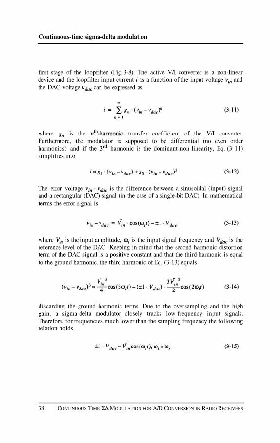
Basically, a continuous-time integrator consists of a capacitor which is charged ordischarged by a current signal. Considering voltage input and voltagefeedback signals a voltage-to-current (V/I) converter is needed to drive the
CONTINUOUS-TIME MODULATION FOR A/D CONVERSION IN RADIO RECEIVERS 37
Continuous-time sigma-delta modulation
first stage of the loopfilter (Fig. 3-8). The active V/I converter is a non-lineardevice and the loopfilter input current i as a function of the input voltage andthe DAC voltage can be expressed as
where is the transfer coefficient of the V/I converter.Furthermore, the modulator is supposed to be differential (no even orderharmonics) and if the harmonic is the dominant non-linearity, Eq. (3-11)simplifies into
The error voltage is the difference between a sinusoidal (input) signaland a rectangular (DAC) signal (in the case of a single-bit DAC). In mathematicalterms the error signal is
where is the input amplitude, is the input signal frequency and is thereference level of the DAC. Keeping in mind that the second harmonic distortionterm of the DAC signal is a positive constant and that the third harmonic is equalto the ground harmonic, the third harmonic of Eq. (3-13) equals
discarding the ground harmonic terms. Due to the oversampling and the highgain, a sigma-delta modulator closely tracks low-frequency input signals.Therefore, for frequencies much lower than the sampling frequency the followingrelation holds
38 CONTINUOUS-TIME MODULATION FOR A/D CONVERSION IN RADIO RECEIVERS

3.2 Theory of sigma-delta modulation
Substituting this result into Eq. (3-14) yields an expression for the third-harmonicof the input signal
Combining Eq. (3-12), Eq. (3-13) and Eq. (3-16) yields the relation between theoutput current and input voltage of a non-linear V/I converter in a modulator.The third harmonic component can be referred to the input of the V/I converter bydividing the second right-hand term of Eq. (3-12) by the linear transfer coefficient
Due to the high gain at low frequencies and the large amount of oversampling, theloop also compensates low-frequency harmonic components. Consequently,
an extra signal at the third harmonic frequency appears in the output spectrumthat is equal to Eq. (3-17). The (low-frequency) third harmonic distortion (HD3)of the continuous-time modulator of Fig. 3-8 equals
Example 3.1: To verify Eq. (3-18), the system of Fig. 3-8 has been simulatedwhere is 1, is 0.0001, and is 0.707 (calculated HD3 is -92 dB).Fig. 3-9 shows the simulated bitstream spectrum. The third-harmoniccomponent (30kHz) is 92 dB down relative to the signal carrier (10 kHz)which is in agreement with the calculated result of Eq. (3-18).
It should be noted that this analysis is only valid for low-frequency signals in theband where the gain of the loopfilter is high. Fig. 3-10 shows the same simulationas in the example, only with a 33.33 kHz input signal. The third-harmonic is at100 kHz where loopfilter gain drops with the order of the loopfilter (4 in thiscase). Because the loopfilter gain drops, the tone at the third-harmonic frequencyof the 33.33 kHz signal component is less suppressed. This effect is not related tothe non-linearity of the integrator and also occurs in an ideal distortion-freemodulator.
CONTINUOUS-TIME MODULATION FOR A/D CONVERSION IN RADIO RECEIVERS 39

Continuous-time sigma-delta modulation
40 CONTINUOUS-TIME MODULATION FOR A/D CONVERSION IN RADIO RECEIVERS
3.2 Theory of sigma-delta modulation
This type of non-linearity is reduced by using a loopfilter with local feedbackpaths (section 3.4.2). With this filter topology an inverse Chebyshev characteristiccan be designed rather than a Butterworth filter. The resonator gains are evenlydistributed in the signal band to reduce the quantization noise (and distortioncomponents) at the end of the signal band and to have a maximally flatquantization noise floor in the signal band.
Another method to suppress the distortion of the non-linear input V/I converters isto use a multi-bit modulator. With a multi-bit DAC, the feedback and inputsignals cancel better than in case of a single-bit feedback signal. However, due tomismatch between the quantization levels, a multi-bit DAC is non-linear andintroduces distortion itself.
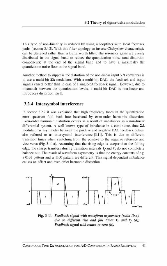
3.2.4 Intersymbol interference
In section 3.2.2 it was explained that high frequency tones in the quantizationerror spectrum fold back into baseband by even-order harmonic distortion.Even-order harmonic distortion occurs as a result of imbalances in a non-lineardifferential system. A well-known type of imbalance in a continuous-timemodulator is asymmetry between the positive and negative DAC feedback pulses,also referred to as intersymbol interference [3.11]. This is due to differenttransition times when switching from the positive to the negative reference andvice versa (Fig. 3-11 a). Assuming that the rising edge is steeper than the fallingedge, the charge transfers during transition intervals and do not completelybalance out. The result of waveform asymmetry is that the energy contents of e.g.a 0101 pattern and a 1100 pattern are different. This signal dependent imbalancecauses an offset and even-order harmonic distortion.
CONTINUOUS-TIME MODULATION FOR A/D CONVERSION IN RADIO RECEIVERS 41

Continuous-time sigma-delta modulation
Example 3.2: Fig. 3-12 shows the simulated result of a modulator with arelative waveform asymmetry error of 0.1% of a full DAC pulse. The inputsignal is at 10 kHz. The second harmonic tone at 20 kHz is 75 dB downrelative to the signal carrier. The noise floor is raised to -120 dB compared tothe spectrum of Fig. 3-5 because of demodulation of high frequencyquantization noise.
Waveform asymmetry can be reduced by short transition intervals and matchingof the transition edges. However, this may not be easy to realize, especially athigher sampling frequencies. A more robust method of improving matching ofwaveforms, is the return-to-zero (RTZ) technique. This technique is shown inFig.3-11b and is based on the principle of resetting each feedback pulse for afraction of the sampling period. As a result, all pulses have a positive and anegative edge, which greatly reduces signal dependence of the mismatch. Now,any mismatch between the positive and negative pulses only affect the offset. Ifthe RTZ interval has a duty-cycle the reference level of the feedback pulseshould increase with the inverse factor in order to have the same charge.Fig.3-11b shows a feedback pulse with a 50% duty cycle
42 CONTINUOUS-TIME MODULATION FOR A/D CONVERSION IN RADIO RECEIVERS

3.2 Theory of sigma-delta modulation
3.2.5 Phase jitter
Fig.3-11b shows the waveform of a typical feedback signal, with a periodicreturn-to-zero state, in a single-bit continuous-time modulator. In the case ofzero rise and fall times, the charge of the feedback pulse is determined by theamplitude of the DAC current and the pulse width where is the pulseduty-cycle, with a value between 0 and 1
Any inaccuracy in the reference charge has a direct impact on the performance ofthe modulator. As described in the previous section, waveform asymmetry is acause for in-band distortion and noise. Besides the inaccuracy of the waveform,also timing uncertainty affects the reference charge in Eq. (3-19). Timinguncertainty is caused by phase noise in the oscillator. A commonly used measureof the total amount of timing noise in the frequency range of interest is the jitterspecification [3.12]. Assuming that jitter can be considered as white noise, withstandard deviation the jitter contributed charge can be expressed by [3.6]
To determine the noise power in the signal band, the power spectral density of thejitter is calculated. The noise power in the signal band can be calculated by
The SNR due to clock jitter is calculated by the ratio between the maximum inputsignal power (Eq. (3-5)) and the jitter power
Example 3.3: In the case of a 50% duty cycle an oversampling ratiom of 64 and of the sampling frequency, the calculated SNR is72 dB. Fig.3-13 shows the simulated output spectrum of a modulator withclock jitter. The quantization noise is not dominant in this simulation. Thesimulated SNR equals 71.8 dB which agrees with the theoretical result (whitenoise assumption).
CONTINUOUS-TIME MODULATION FOR A/D CONVERSION IN RADIO RECEIVERS 43

Continuous-time sigma-delta modulation
It should be noted that Eq. (3-22) only applies to a feedback pulse with a periodicreturn-to-zero state. In the case of a full period feedback pulse withoutreturn-to-zero, the jitter power depends on the relative number of edges in abitstream sequence. This can be easily understood considering a 11110000 and a01010101 bitstream sequence (no return-to-zero). A timing uncertainty onlyoccurs at the edge when the feedback pulse changes from 0 to 1 or vice versa.Obviously, the jitter power of the first sequence is smaller than the second one,due to the difference in number of transitions (1 versus 7). This implies that thejitter power is signal dependent and becomes larger for smaller input signals.
3.2.6 Aliasing
Due to the sampling process, any input frequency which is larger than half thesampling frequency will reflect into the frequency range This isthe known problem of aliasing. Reduction of the aliasing effect is achieved bymeans of an analog filter in front of the sampler, to suppress the energy content ofthe frequency bands at multiples of the sampling frequency. An importantproperty of a continuous-time modulator is that the sampling takes place at theoutput of the continuous-time loopfilter (in contrast to a discrete-timemodulator where sampling is done at the input of the loopfilter). The loopfilter
44 CONTINUOUS-TIME MODULATION FOR A/D CONVERSION IN RADIO RECEIVERS
3.2 Theory of sigma-delta modulation
operates as an anti-aliasing filter, therefore discarding the need for an anti-aliasingfilter in front of the modulator. The suppression of an aliasing component,originating from an input signal with a frequency close to the sampling frequency,can be easily calculated, using the linear model of a continuous-timemodulator (Fig. 3-15). Under the assumption that the hold function in thefeedback path is a lowpass filter with a gain of 1 at low frequencies and a gain of0 for frequencies near the sampling frequency, it is shown in [3.6] that the aliasingcomponent of an input signal with frequency is reduced by the loopfilterwith a factor
where is the loopfilter gain for the low frequency aliased component atand the gain for the input frequency close to the sampling frequency.
Example 3.4: A modulator with the fifth-order feedforward compensatedloopfilter characteristic of Fig. 3-24 has been simulated. The simulation resultis shown in Fig. 3-14 for a -9 dB input signal at The aliasedcomponent occurs at and is suppressed by about 80 dB.
CONTINUOUS-TIME MODULATION FOR A/D CONVERSION IN RADIO RECEIVERS 45

Continuous-time sigma-delta modulation
3.3 Linear stability analysis
Stability is an important issue in the design of a modulator and yet, due to thefact that the quantizer is a non-linear element, it has not been possible to find amathematical solution for guaranteed loop stability of higher-order modulators.However, a useful insight to stability is obtained by the analysis of limit cycles, oridling tones, in the output signal of the modulator. A stable modulatorexhibits out-of-the-band limit cycles at fractions of the sampling frequency whichdo not affect the SNR [3.13]. In contrast, the SNR of an unstable modulator isdeteriorated by low-frequency limit cycles, due to an output of alternating longstrings of 1s and 0s [3.2] that may have unbounded states. Numerous methods forstability analysis and rules of thumb have been presented [3.14]- [3.15] whichare valuable for higher-order modulator design. In this section a linearquantizer model is used for stability analysis [3.16], [3.17]. With this linear modelthe root locus method can be applied to analyze the linearized system for stablelimit cycles. First, stability of a modulator in the case of a small input signal isdiscussed, followed by the large signal stability analysis.
3.3.1 Small signal stability
Fig. 3-15 shows a linear model of a continuous-time (CT) modulator. Thesystem consists of a CT loopfilter with transfer function H(s) and a sampledquantizer. The quantizer is modeled with a linear gain and a phase shiftThe quantizer output, which is a train of pulses, is fed back through a D/Aconverter, being a zero-order hold function, and subtracted from the analog inputsignal.
It is assumed that the input of the quantizer is a sinusoidal waveform. The gainof the quantizer can be defined as the ratio between the input power and the
46 CONTINUOUS-TIME MODULATION FOR A/D CONVERSION IN RADIO RECEIVERS

3.3 Linear stability analysis
output power of the quantizer. The sampling of the quantizer introduces afrequency dependent phase uncertainty in the loop [3.18] for input frequencieswhich are rational fractions of the sampling frequency [3.19]. This means that fora certain range of phases, the quantizer produces the same output pattern,regardless of the phase of the input signal. This is explained by Fig.3-16 for asinusoidal quantizer input signal with frequency in the case of a one-bitquantizer. Consider the sinusoidal signal in Fig.3-16 (solid line). Both at samplemoments and the quantizer gives a positive output. At samplemoment the quantizer output is negative. After four sample moments theoutput pattern is repetitive. If the (solid) sinusoidal signal is shifted in phase overa range of (dotted lines in Fig.3-16) the quantizer output gives the exact sameoutput pattern for the whole range of phases. Thus, the quantizer is not able todetect the phase of an input signal at and therefore has a phase uncertainty. At
the maximum phase uncertainty is This uncertainty in phase of thequantizer is largest at In the Laplace domain, the quantizer is modeledas
CONTINUOUS-TIME MODULATION FOR A/D CONVERSION IN RADIO RECEIVERS 47
where is the quantizer gain and the phase shift.

48 CONTINUOUS-TIME MODULATION FOR A/D CONVERSION IN RADIO RECEIVERS
Due to the exponential terms in Eq. (3-27) there is no analytical expression whichcan solve this characteristic equation. With numerical analysis, the root locus ofthe second-order system has been determined (Fig.3-17). Fig.3-17 shows that thepoles which are starting from the origin, move directly into the right-half planefor any gain and any phase Hence, the linear model of a second-ordermodulator is unstable for any quantizer gain and phase. To stabilize thesecond-order modulator, a zero can be introduced in the filter transfer function of
The filter characteristic has two poles and for simplicity, the DC gains of bothintegrators have been considered to be infinite (ideal integrators). With thetransfer functions of Eq. (3-24), Eq. (3-25), and Eq. (3-26), the characteristicequation of the linear system of Fig. 3-15 can be determined
With the linear model of Fig. 3-15, the modulator can be analyzed using theroot locus method, which shows the closed loop poles as a function of thequantizer gain for different phase shifts of the quantizer. The modulator is stableif all poles are in the left-half plane of the root locus plot. Stability of amodulator becomes an issue if the loopfilter order is larger than 1. In thefollowing, stability of a modulator with a second-order loopfilter is discussed.A second-order lowpass loopfilter consists of two integrator stages which areconnected in cascade. The transfer function of a second-order integrator filter isgiven by
The DAC in the feedback path has the function of a zero-order hold
For signals that are not rational fractions of the sampling frequency, any shift inphase always gives a change in the quantizer output pattern. Therefore, the phaseuncertainty for those frequencies is zero.
Continuous-time sigma-delta modulation
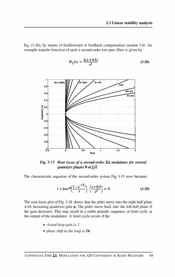
3.3 Linear stability analysis
Eq. (3-26), by means of feedforward or feedback compensation (section 3.4). Anexample transfer function of such a second-order low-pass filter is given by
The characteristic equation of the second-order system Fig. 3-15 now becomes
The root locus plot of Fig. 3-18 shows that the poles move into the right-half planewith increasing quantizer gain The poles move back into the left-half plane ifthe gain decreases. This may result in a stable periodic sequence, or limit cycle, atthe output of the modulator. A limit cycle occurs if the
CONTINUOUS-TIME MODULATION FOR A/D CONVERSION IN RADIO RECEIVERS 49
closed-loop gain is 1
phase shift in the loop is

Continuous-time sigma-delta modulation
The gain and phase shift of the loopfilter and the zero-order hold function aredetermined for all frequencies. Therefore, a limit cycle exists if there is a solutionfor the gain and the phase of the quantizer such that the criteria above are met. Itwas observed from Fig. 3-16 that the quantizer phase range is large at
the filter gain and phase are 1.336 and while the gain andphase shift of the zero-order hold function are 0.9 and respectively. Takinginto account the sign inversion of the feedback path the quantizer phaseshift must be
at (equal to at and the quantizer gain
for a limit cycle at
50 CONTINUOUS-TIME MODULATION FOR A/D CONVERSION IN RADIO RECEIVERS

3.3 Linear stability analysis
Fig. 3-18 shows the root locus plot of the second-order modulator for severalquantizer phases. At a quantizer phase of the root locusenters the right-half plane at The quantizer gain at this intersection point isequal to the result of Eq. (3-31). Fig. 3-19 shows the simulated output spectrum ofthe second-order loopfilter with the transfer function of Eq. (3-28), in the case of avery small input signal. In this simulation the limit cycle at is dominant.
3.3.2 Large signal stability
In the previous section, stability of a second-order modulator for small inputsignals was discussed. If the amplitude of the input signal increases, the quantizergain decreases and the poles of a higher-order modulator may eventually bepushed into non-stable locations. The reason for this instability is that the inputsignal becomes too large to be compensated for by the feedback signal. Typically,the maximum specified input signal ranges from 50% to 80% of the rms-value ofthe DAC feedback signal [3.2]. Large signal instability also becomes visible froma root locus plot of a fifth-order modulator in Fig. 3-21 (example quantizer phaseis at The loopfilter of this fifth-order modulator has 5 poles and fourzeros. If the quantizer gain drops below two poles shift into the right-half plane
CONTINUOUS-TIME MODULATION FOR A/D CONVERSION IN RADIO RECEIVERS 51

Continuous-time sigma-delta modulation
and the system becomes unstable. The gain determines the maximumallowable input signal level for a stable modulator.
An effective method to preserve the stability of a modulator at overload is tolimit the maximum output swings of the loopfilter integrator stages. By limitingthe integrator swings, the quantizer gain is prevented from dropping below thestable value Fig. 3-20 shows a fifth-order modulator with limiters in the third,fourth and fifth filter stages. The feedforward paths with gains are needed tocreate the zeros in the loopfilter for stability of the loop (section 3.4.1). The filtercoefficients should be scaled in such a way that, at an increasing overload inputlevel, the integrator outputs are limited one by one, starting with the last integratorstage. As a result, the modulator order is degraded from fifth to fourth, to thirdand finally a second-order modulator remains which is always stable for largeinput signals (Fig. 3-18). If the input level drops from the overload state to a lowerstable value again, stable fifth-order behavior is retrieved. Another technique toensure large signal stability is to monitor the number of consecutive equal bits inthe digital domain. In general, the maximum number of equal bits in a row is inthe order of 10 bits for a stable modulator which is not in overload. If the numberof bits becomes too large the integrator outputs are reset, by switching theintegrator outputs to a zero reference. The resetting of the integrator statescontinues as long as the modulator remains in overload.
52 CONTINUOUS-TIME MODULATION FOR A/D CONVERSION IN RADIO RECEIVERS

3.4 High-frequency stability compensation
3.4 High-frequency stability compensation
In this section, the design of higher-order filters is presented. Feedforward andfeedback compensation techniques are described for high frequency stability ofthe loop. Both compensation techniques can provide the same noise transferfunction but have different signal transfer characteristics. Butterworth and inverseChebyshev noise transfer functions are shown. Finally, a comparison is madebetween the two compensation techniques.
3.4.1 Feedforward compensation
Increasing the order of the loopfilter of a modulator provides more aggressivequantization noise-shaping and efficiently improves signal-to-quantization noiseratio (section 3.2.1).
CONTINUOUS-TIME MODULATION FOR A/D CONVERSION IN RADIO RECEIVERS 53
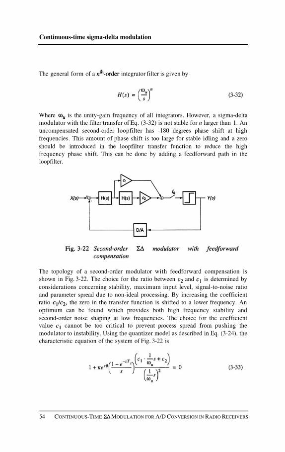
Continuous-time sigma-delta modulation
The general form of a integrator filter is given by
Where is the unity-gain frequency of all integrators. However, a sigma-deltamodulator with the filter transfer of Eq. (3-32) is not stable for n larger than 1. Anuncompensated second-order loopfilter has -180 degrees phase shift at highfrequencies. This amount of phase shift is too large for stable idling and a zeroshould be introduced in the loopfilter transfer function to reduce the highfrequency phase shift. This can be done by adding a feedforward path in theloopfilter.
The topology of a second-order modulator with feedforward compensation isshown in Fig. 3-22. The choice for the ratio between and is determined byconsiderations concerning stability, maximum input level, signal-to-noise ratioand parameter spread due to non-ideal processing. By increasing the coefficientratio the zero in the transfer function is shifted to a lower frequency. Anoptimum can be found which provides both high frequency stability andsecond-order noise shaping at low frequencies. The choice for the coefficientvalue cannot be too critical to prevent process spread from pushing themodulator to instability. Using the quantizer model as described in Eq. (3-24), thecharacteristic equation of the system of Fig. 3-22 is
54 CONTINUOUS-TIME MODULATION FOR A/D CONVERSION IN RADIO RECEIVERS
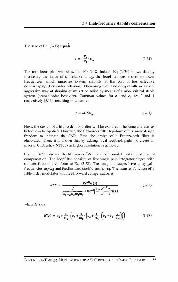
3.4 High-frequency stability compensation
*The zero of Eq. (3-33) equals
The root locus plot was shown in Fig. 3-18. Indeed, Eq. (3-34) shows that byincreasing the value of relative to the loopfilter zero moves to lowerfrequencies which improves system stability at the cost of less effectivenoise-shaping (first-order behavior). Decreasing the value of results in a moreaggressive way of shaping quantization noise by means of a more critical stablesystem (second-order behavior). Common values for and are 2 and 1respectively [3.13], resulting in a zero of
Next, the design of a fifth-order loopfilter will be explored. The same analysis asbefore can be applied. However, the fifth-order filter topology offers more designfreedom to increase the SNR. First, the design of a Butterworth filter iselaborated. Then, it is shown that by adding local feedback paths, to create aninverse Chebyshev NTF, even higher resolution is achieved.
Figure 3-23 shows the fifth-order modulator model with feedforwardcompensation. The loopfilter consists of five single-pole integrator stages withtransfer functions conform to Eq. (3-32). The integrator stages have unity-gainfrequencies and feedforward coefficients The transfer function of afifth-order modulator with feedforward compensation is
CONTINUOUS-TIME MODULATION FOR A/D CONVERSION IN RADIO RECEIVERS 55
where H(s) is
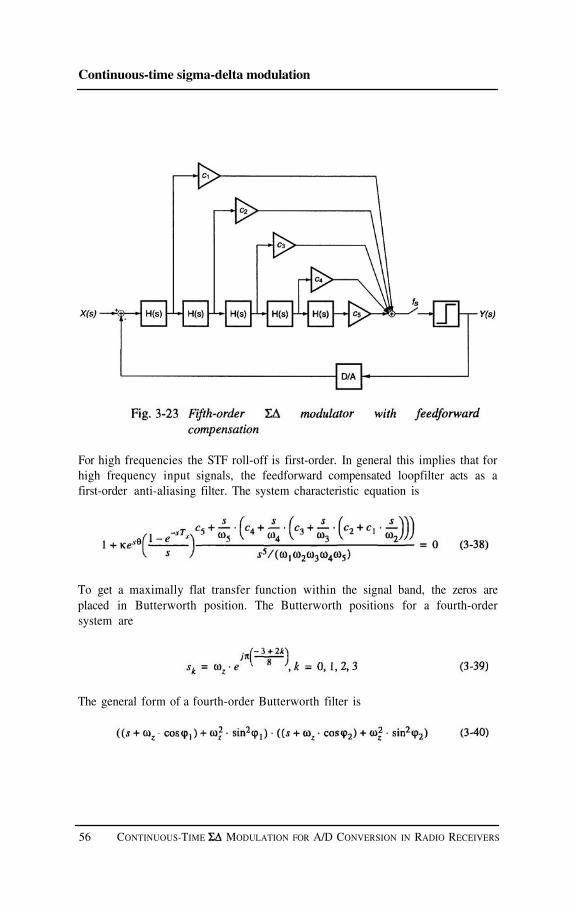
Continuous-time sigma-delta modulation
For high frequencies the STF roll-off is first-order. In general this implies that forhigh frequency input signals, the feedforward compensated loopfilter acts as afirst-order anti-aliasing filter. The system characteristic equation is
To get a maximally flat transfer function within the signal band, the zeros areplaced in Butterworth position. The Butterworth positions for a fourth-ordersystem are
The general form of a fourth-order Butterworth filter is
56 CONTINUOUS-TIME MODULATION FOR A/D CONVERSION IN RADIO RECEIVERS

3.4 High-frequency stability compensation
where and are the angles of the zeros in the complex plane relative to theimaginary axis, which are calculated by Eq. (3-39). In order to place the zeros ofthe characteristic equation in Butterworth positions Eq. (3-37) and Eq. (3-40)should be equal. This results in five relations to calculate the desired coefficients
or, in general,
where is the Butterworth coefficient and n the loopfilter order. TheButterworth coefficients of a fifth-order filter are
Figure 3-24 shows an example of a Bode plot of the fifth-order filter. At lowfrequencies the filter characteristic rolls off fifth-order and the phase shift closelyreaches -450 degrees (at radians). At high frequencies the filter becomes
CONTINUOUS-TIME MODULATION FOR A/D CONVERSION IN RADIO RECEIVERS 57

Continuous-time sigma-delta modulation
first-order and the phase turns back to about -97 degrees at half the samplingfrequency. In general, any order of filter can be designed according to theprocedure as discussed in this section. However, further increasing the filter orderpushes the zero locations to lower frequencies for a stable system. Hence,increasing the filter order decreases the effective bandwidth where quantizationnoise is shaped to a low enough level. Because of the fifth-order shaping, lowfrequency quantization noise is very small and rises fifth-order with frequency.Therefore, total in-band quantization noise is dominantly determined by thequantization noise at the end of the signal band. This severely limits themaximum obtainable bandwidth. An effective way to shape the end-of-the-bandquantization noise is to apply local feedback paths in the loopfilter which createresonator stages. The resonator stages can provide some extra notch gain at theend of the signal band which suppresses the large amount of quantization noisethat is present here. The design of a loopfilter with local feedback paths will bediscussed next.
58 CONTINUOUS-TIME MODULATION FOR A/D CONVERSION IN RADIO RECEIVERS

3.4 High-frequency stability compensation
3.4.2 Feedforward compensation and local feedback
Applying feedback around two integrator stages shifts the DC gain of theintegrators to a finite resonance frequency. This way, the gain can be spread moreequally in the signal band which, for example, is important for suppression ofquantization noise at the end of the signal band. The general transfer function of aresonator is
With local feedback paths it is possible to implement an inverse Chebyshev NTFrather than a Butterworth NTF. Fig. 3-25 shows the general model of a fifth-ordermodulator with feedforward and local feedback paths.
The feedforward coefficients and the integrator unity gain frequencies remainunchanged while the local feedback coefficients and determine the notchfrequencies of the resonators according to
CONTINUOUS-TIME MODULATION FOR A/D CONVERSION IN RADIO RECEIVERS 59
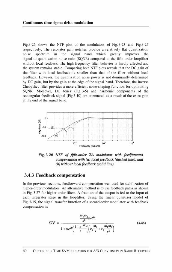
Continuous-time sigma-delta modulation
Fig.3-26 shows the NTF plot of the modulators of Fig. 3-23 and Fig.3-25respectively. The resonator gain notches provide a relatively flat quantizationnoise spectrum in the signal band which greatly improves thesignal-to-quantization-noise ratio (SQNR) compared to the fifth-order loopfilterwithout local feedback. The high frequency filter behavior is hardly affected andthe system remains stable. Comparing both NTF plots reveals that the DC gain ofthe filter with local feedback is smaller than that of the filter without localfeedback. However, the quantization noise power is not dominantly determinedby DC gain, but by the gain at the edge of the signal band. Therefore, the inverseChebyshev filter provides a more efficient noise-shaping function for optimizingSQNR. Moreover, DC tones (Fig. 3-5) and harmonic components of therectangular feedback signal (Fig.3-10) are attenuated as a result of the extra gainat the end of the signal band.
3.4.3 Feedback compensation
In the previous sections, feedforward compensation was used for stabilization ofhigher-order modulators. An alternative method is to use feedback paths as shownin Fig. 3-27 for higher-order filters. A fraction of the output is fed to the input ofeach integrator stage in the loopfilter. Using the linear quantizer model ofFig. 3-15, the signal transfer function of a second-order modulator with feedbackcompensation is
60 CONTINUOUS-TIME MODULATION FOR A/D CONVERSION IN RADIO RECEIVERS

3.4 High-frequency stability compensation
The characteristic equation is equal to the denominator of Eq. (3-47)
This relation is similar to the characteristic equation of the feedforwardcompensated system of Fig. 3-22.
3.4.4 Feedback compensation and local feedback
Fig. 3-28 shows a fifth-order modulator with feedback compensation. The STFof this modulator is
where are coefficients
As has been the case for the second-order filter, the STF of the fifth-order filterwith feedback compensation does not have zeros (assuming is 0). Thus, the STF
CONTINUOUS-TIME MODULATION FOR A/D CONVERSION IN RADIO RECEIVERS 61

Continuous-time sigma-delta modulation
of a feedback compensated modulator is a lowpass filter.The characteristic equation equals
For a maximal flat filter transfer, the coefficients are placed in Butterworthpositions, according to Eq. (3-40).
With local feedback paths, the Butterworth NTF can be changed into an inverseChebyshev NTF, to optimize the noise-shaping function. Fig. 3-29 shows thefeedback compensated topology with local feedback. Again, the filter coefficientsare determined following the same method as in section 3.4.2.
62 CONTINUOUS-TIME MODULATION FOR A/D CONVERSION IN RADIO RECEIVERS

3.4 High-frequency stability compensation
3.4.5 Feedforward versus feedback compensation
It has been shown that compensation of a higher-order loopfilter with feedforwardor feedback paths, yields similar relations for the characteristic equation. Thus,for stability of the loop, both compensation techniques can be used successfully.Nevertheless, some essential differences exist between the two topologies.
The STFs of the feedforward and feedback compensated loopfilters are given byEq. (3-36) and Eq. (3-48) respectively. Generally, the STF of anfeedforward compensated filter has n poles and n-1 zeros, while the feedbackcompensated STF has n poles only. Therefore, the feedforward STF is afirst-order lowpass anti-aliasing filter, while the feedback STF is anlowpass anti-aliasing filter. This is shown graphically in Fig. 3-30 for thefifth-order modulators as described in section 3.4.1 and section 3.4.3. Clearly, thefeedback STF provides much stronger filtering for high frequency signals than thefeedforward STF. A second difference between the STFs can be observed fromFig. 3-30 as well. It is shown that, due to the zeros of the feedforward filters, theSTF is not flat at low frequencies for the choice of filter coefficients as derivedearlier. Because of the non-ideal compensation of STF poles and zeros, the STFshows peaking at a certain frequency. This implies that at the peaking frequencythe maximum stable input level is reduced by the gain of the peaking. Because theSTF has no zeros, the feedback filter does not suffer from significant peaking.
A major drawback of the feedback filter architecture is that the outputs of theintegrators contain, besides filtered quantization noise, a substantial part of theinput signal [3.2]. The unity gain frequencies of the lower order integrators(especially the first integrator) in a feedback filter have to be much lower than inthe case of a feedforward filter, in order to keep the output signal swing within the
CONTINUOUS-TIME MODULATION FOR A/D CONVERSION IN RADIO RECEIVERS 63

Continuous-time sigma-delta modulation
available supply range. Thus, noise and distortion of the higher-order integratorscan not be neglected as they are not heavily suppressed by a high gain of theprevious integrator stages. This can be a serious problem, especially if theoversampling ratio is low. As a result, power consumption of the feedbackarchitecture tends to be higher than that of a feedforward architecture. This is themain reason why feedforward filters have been used for the designs in this book.It should be noted that by combining feedforward and feedback compensationtechniques, more freedom is obtained for an optimal filter design.
3.5 Quadrature sigma-delta modulation
In the previous section, the design of higher-order lowpass filters was discussedfor application in a modulator with real input signals. The poles and zeros ofthe filter are real and complex-conjugate pairs, due to the real-valued filtercoefficients. If two modulators with real filters are used in a quadratureconfiguration (Fig. 2-7), with complex input I + jQ, the magnitude response issymmetrical around DC. By using complex-valued coefficients, the filter transferis not constrained to having complex-conjugate pairs of poles or zeros [3.20] andit can be asymmetrical around DC. This will be shown for a complex integrator insection 3.5.1. Then, the design of a complex fifth-order filter is shown as anexample. Again, both feedforward and feedback frequency compensationtechniques can be used in a complex filter for stability.
3.5.1 Complex integrator
A complex integrator consists of two real integrator stages, with quadrature inputsignals, which are cross-coupled. The model of a continuous-time complexintegrator is shown in Fig. 3-31. The transfer of the complex integratorequals
The transfer of Eq. (3-51) is almost identical to the transfer of a real integrator,with the difference that the frequency independent part in the denominator is acomplex number. The coefficient e causes a shift in the frequency domain of thereal transfer H(s) into the position of the complex transfer This is showngraphically in Fig. 3-32 for the NTF of a first-order modulator with the filter
64 CONTINUOUS-TIME MODULATION FOR A/D CONVERSION IN RADIO RECEIVERS

3.5 Quadrature sigma-delta modulation
transfer of Eq. (3-51), for e is 0, e is +0.1 and e is -0.2. If e is zero, thecomplex transfer is equal to the real transfer H(s) and the NTF issymmetrical around DC with the gain notch at DC (Fig.3-32a). If e is not equal tozero, the NTF shifts from DC to The unity gain frequency of isequal to
For small values of e (e < 0.1) the unity-gain frequency only slightly changesrelative to the unity-gain frequency of a real integrator. This implies that stabilityof a modulator is hardly affected in case the loopfilter consists of complexintegrators. If the value of e becomes closer to one, the stability coefficients mustbe recalculated with the unity gain frequency of Eq. (3-52). If the feedbackcoefficient e has a negative value, the gain notch of the complex transfer function
shifts into the negative frequency plane. Fig.3-32b and Fig.3-32c show theNTFs in the case e has a positive and a negative value respectively. This way, it ispossible to shift the gain notches of all complex integrators in a complexfilter into the positive (or negative) frequency plane for strong quantization noisesuppression. This is shown in the next section.
CONTINUOUS-TIME MODULATION FOR A/D CONVERSION IN RADIO RECEIVERS 65

Continuous-time sigma-delta modulation
3.5.2 Complex filter design
Fig. 3-33 shows the model of a fifth-order quadrature baseband modulatorwith feedback compensation. The gain notches of the 5 complex integrators canbe shifted into the positive frequency plane and distributed within the signal band.Such a fifth-order NTF of a quadrature modulator is shown in Fig. 3-34. The firstnotch of the NTF is at DC, which means that one of the complex cross-couplingcoefficients is equal to zero. The notches are positioned such, that the NTF is flatwithin the signal band. With 5 notches, a deep suppression of quantization errorswithin the signal band is obtained. Outside the signal band, the NTF risesfifth-order.
An ideal fifth-order complex baseband modulator with the NTF characteristicof Fig. 3-34 has been simulated and the bitstream output spectrum is shown inFig.3-36. As expected, quantization noise within the signal band is very low andthe theoretical obtainable SQNR is high. In practice, the SQNR will be impairedby non-ideal effects. The most important error sources are process related, whichare parameter mismatch and spread. As we are dealing with a complex system,the problem of image interference arises, as explained in section 2.4.3. Because ofthe asymmetrical NTF, the quantization noise in the image band is notsuppressed, as can be seen from Fig. 3-36. Therefore, quantization noise power inthe image band is very large. In case of a mismatch between the quadraturefeedback signals in a complex modulator, part of the quantization noise power inthe image band ‘leaks’ into the signal band and vice versa [3.20]- [3.22]. Thiseffect has been simulated and Fig. 3-37 shows the output spectrum of the complex
modulator in the case of 0.5% mismatch between the quadrature feedback
66 CONTINUOUS-TIME MODULATION FOR A/D CONVERSION IN RADIO RECEIVERS

3.5 Quadrature sigma-delta modulation
signals. Because of the high quantization noise power in the image band, theSQNR can be affected considerably, as a result of image interference.
To reduce the effect of quantization noise leakage from the negative band in thepositive band, the matching between the quadrature signals should be improved.A powerful technique to improve matching is dynamic element matching. This isdiscussed in detail in chapter 5. A second method is to reduce the quantizationerror power in the image band. This can be done by shifting one integrator notchin the image band at the cost of less effective quantization error suppression in thesignal band [3.20]. The NTF of the fifth-order complex modulator is shown inFig. 3-35. Because quantization noise power is largest at the end of the imageband, the integrator notch is placed close to the end of the band. Because of theloss of an integrator notch, the quantization noise suppression in the signal bandis lower than in Fig. 3-34.
Process spread is another non-ideality which can seriously affect SQNRperformance. This problem especially applies to the complex modulatortopology because of the very high in-band quantization noise suppression. Anyfrequency shift of the integrator notches, in particular the notch at the end of thesignal band, deteriorates SQNR. The filter coefficients and unity-gain frequencies
CONTINUOUS-TIME MODULATION FOR A/D CONVERSION IN RADIO RECEIVERS 67

Continuous-time sigma-delta modulation
rely on absolute component values rather than ratios. Due to non-idealprocessing, the absolute value can spread with 10-20%. Therefore, coefficientcalibration is highly recommended for this kind of filter
68 CONTINUOUS-TIME MODULATION FORA/DCONVERSION IN RADIO RECEIVERS

3.5 Quadrature sigma-delta modulation
CONTINUOUS-TIME MODULATION FOR A/D CONVERSION IN RADIO RECEIVERS 69

Continuous-time sigma-delta modulation
References
[3.1] Cutler, C.C., “Transmission system employing quantization,” U.S.Patent No. 2,927,962, March 8, 1960 (filed 1954).
[3.2] Norsworthy, S.R., R. Schreier, G.C. Temes, Delta-sigma dataconverters - Theory, design, and simulation, IEEE Press, New York,1997.
[3.3] Inose, H., Y. Yasuda, and J. Murakami, “A telemetering system bycode modulation,” IRE Trans. Space Electron.Telemetry, vol. SET-8, pp. 204-209, Sept. 1962.
[3.4] Jager, F. de, “Delta modulation - a method of PCM transmissionusing the one unit code,” Philips Res. Rep., vol. 7, pp. 442-466,1952.
[3.5] Bennett, W.R., “Spectra of quantized signals,” Bell Syst. Tech. J.,vol. 27, pp. 446-472, Jul. 1948.
[3.6] Zwan, E.J. van der, E.C. Dijkmans, “A 0.2 mW CMOSmodulator for speech coding,” IEEE J. Solid-State Circuits, vol. 31,pp. 1873-1880, Dec. 1996.
[3.7] Schuchman, L., “Dither signals and their effect on quantizationnoise,” IEEE Trans. Commun. Tech., vol. COM-12, pp. 162-165,Dec. 1964.
[3.8] LaMay, J.L., and H. T. Bogard, “How to obtain maximum practicalperformance from state-of-the-art delta-sigma analog-to-digitalconverters,” IEEE Trans. Instr. Meas., vol. 41, pp. 861-867, Dec.1992.
[3.9] Breems, L.J., E.J. van der Zwan, E.C. Dijkmans and J.H. Huijsing,“A 1.8 mW CMOS Modulator with Integrated Mixer for A/DConversion of IF Signals,” ISSCC Dig. Tech. Papers, pp. 64-65, Feb.1999.
[3.10] Breems, L.J., E.J. van der Zwan, J.H. Huijsing, “Design forOptimum Performance-to-Power Ratio of a Continuous-timeModulator,” Proc. of ESSCIRC, pp. 318-321, Sep. 1999.
[3.11] Adams, R.W., “Design and implementation of an audio 18-bitanalog-to-digital converter using oversampling techniques,” J.Audio Eng. Soc., vol. 34, pp. 153-166, Mar. 1986.
[3.12] Westra, J.R., High-performance oscillators and oscillator systems.Ph.D. thesis, Delft University of Technology, 1998.
[3.13] Plassche, R. van der, Integrated analog-to-digital anddigital-to-analog converters, Kluwer Academic Publishers,Dordrecht, 1994.
70 CONTINUOUS-TIME MODULATION FOR A/D CONVERSION IN RADIO RECEIVERS

3.5 Quadrature sigma-delta modulation
[3.14] Kirk, C.-H, Chao, Shujaat, N., Wai L. Lee, and Charles G. Sodini,“A higher order topology for interpolative modulators foroversampling A/D converters,” IEEE Trans. on Circuits andSystems, vol. 37, pp. 309-318, Mar. 1990.
[3.15] Bhagawati, P.A., K. Shenoi, “Design methodology for IEEETrans. on Communications, vol. 31, pp. 360-370, Mar. 1983.
[3.16] Atherton, D.P., Stability of non-linear systems, Research Studiespress; Wiley, ISBN 0-387-94582-2, 1981.
[3.17] Ardalan, S.H., and J.J. Paulos, “Analysis of nonlinear behavior indelta-sigma modulators,” IEEE Trans. Circuits Sys., vol. 34, pp.593-603, June 1987.
[3.18] Hoffelt, M.H., “On the stability of a 1-bit quantized feedbacksystem,” Proc. of ICASSP, pp. 844-848, 1979.
[3.19] Engelen, J. van, Stability analysis and design of bandpass sigmadelta modulators, Ph.D. thesis, Technische Universiteit Eindhoven,1999.
[3.20] Jantzi, S.A., K.W. Martin, A.S. Sedra, “Quadrature bandpassmodulation for digital radio,” IEEE J. Solid-State Circuits, vol. 32,pp. 1935-1950, Dec. 1997.
[3.21] Jantzi, S.A., K. Martin, A.S. Sedra, “A quadrature bandpassdelta-sigma modulator for digital radio,” ISSCC Dig. Tech. Papers,pp. 216-217, Feb. 1997.
[3.22] Jantzi, S.A., K.W. Martin and A.S. Sedra, “Mismatch effects incomplex bandpass modulators,” Proc. of ISCAS, vol. 1, pp.227-230, May 1996.
CONTINUOUS-TIME MODULATION FOR A/D CONVERSION IN RADIO RECEIVERS 71

Realization of anIF-to-basebandsigma-delta modulator 4
4.1 Introduction
In this chapter the theory, design, and experimental results of a continuous-timemodulator with an integrated mixer are presented. This IF-to-baseband
modulator has the functions of a mixer, anti-aliasing filter, and A/D converter.Key features of this topology are its low-power consumption (1.8 mW) and highlinearity (-84 dB IM3). In section 4.2 a general overview is given of two different
modulator architectures which incorporate frequency translation inside andoutside the loop. It is shown that non-idealities of the mixer can result inmodulation of high-frequency quantization noise into the frequency band ofinterest. In the final part of the section, the topologies are compared. Insection 4.3, the integrated design of a passive mixer and an RC filter is shown thatis used for the input stage of the IF modulator. Important aspects concerninglinearity, mixer driving and self-mixing are discussed. Mathematical derivationsgive ‘rule-of-thumb’ relations between design parameters, such as biasing currentand transistor dimensions, and performance figures, like noise and distortion. Insection 4.4 the complete modulator topology is presented and the design ofthe individual blocks are shown. The experimental results of two realizedprototype chips are given in section 4.5. In section 4.6 conclusions are drawn.
CONTINUOUS-TIME MODULATION FOR A/D CONVERSION IN RADIO RECEIVERS 73

Realization of an IF-to-baseband sigma-delta modulator
4.2 Frequency translation in sigma-delta modulators
In this section, two topologies for IF-to-baseband conversion in a modulatorare shown which incorporate a mixer inside (section 4.2.1) and outside(section 4.2.2) the loop of a baseband modulator. An important requirement isthat an independent choice can be made for the LO frequency of the mixer and thesampling frequency of the modulator. If not related, the sampling rate can beoptimized for dynamic range performance and power consumption of themodulator, without affecting the LO frequency, which is often set by theapplication. In section 4.2.3, both topologies are compared and conclusions aredrawn.
4.2.1 Mixer inside the sigma-delta loop
In this section modulator topologies are investigated with the mixer inside thesigma-delta loop. Fig.4-1 shows a general model of a single-loop modulatorwith a mixer inside the loop. The IF input signal X is mixed with the LOfrequency and translated to baseband by the mixer in the forward path(mixer1 in Fig.4-1). The baseband signal is further processed by a lowpassloopfilter and digitized. The feedback signal needs to be upconverted by a secondmixer (mixer2 in Fig.4-1) to compensate for the downconversion mixer in theforward path. The input signal X is adjusted by the gain of the mixer in theforward path only, while the quantizer error passes both mixers in the loop and itsgain is not affected. Therefore, the maximum allowable input level(non-overload) is adjusted by the gain of the mixer. The stability of themodulator is not affected, because the two mixers in the loop cancel each other.
74 CONTINUOUS-TIME MODULATION FOR A/D CONVERSION IN RADIO RECEIVERS

4.2 Frequency translation in sigma-delta modulators
The main advantage of placing the mixer inside the loop is that non-idealitiesof the mixer in the forward path (mixer1), like non-linearity, are suppressed by theloopgain. This is the case for modulators with a multi-bit DAC (section 3.2.3)or if the feedback path incorporates an analog filter [4.1]. If a modulator has asingle-bit DAC without a filter in the feedback path, the mixer non-idealities arenot suppressed by the loop. Note that the non-linearity of the mixer in thefeedback path (mixer2) is also not suppressed by the loop. If the LO frequency isa rational fraction of the sampling frequency, the frequency translation of thefeedback signal (mixer2) can be easily performed in the digital domain withperfect linearity.
Due to the continuous-time nature of the signals, the continuous-time system ofFig.4-1 is sensitive to parasitic delay between the mixers. If mixing of thefeedback signal is done in the digital domain, parasitic delay in the DAC adds tothe total delay. A delay between the two mixers can be modeled as a delaybetween the LO signals of both mixers. This is shown in the time domain inFig.4-2a, which shows delayed clock signals LO (mixerl) and LO’ (mixer2), theoutput signal Y, and the mixer1 output W. In this example, the LO frequency isequal to half the sampling frequency. During a small time interval the outputsignal Y passes the mixers in the feedback and feedforward path, while beingmodulated only once. In the frequency domain, this implies that a fraction of thenoise band around the LO carrier in the output bitstream spectrum is folding intothe signal band, which can deteriorate system performance.
CONTINUOUS-TIME MODULATION FOR A/D CONVERSION IN RADIO RECEIVERS 75

Realization of an IF-to-baseband sigma-delta modulator
This effect has been simulated in the case of a delay of 0.1% of the LO periodbetween the LO signals of both mixers (Fig.4-3a). Again, the LO frequency ischosen equal to half the sampling frequency A -20 dB sinusoidal signal,modulated at the LO frequency with a small offset frequency of has beenapplied to the input of the system of Fig. 4-1. Fig. 4-3b shows the same simulation,without any delay. Clearly, the noise floor is considerably higher in case of asmall delay, compared to the ideal simulation. This effect is considerably reducedif the LO frequency is close to the sampling frequency. Around the samplingfrequency, quantization noise is greatly suppressed by the loopfilter, and noiseleakage into baseband will be much less severe.
A method to overcome the delay problem is the use of DAC pulses withreturn-to-zero. Fig.4-2b again shows the LO waveforms of the mixers and theDAC signal, now with RTZ. Due to the RTZ intervals, the DAC is insensitive to adelay between the LO signals as long as the delay falls within the RTZ interval.This way the LO frequency can be a rational fraction of the sampling frequency,without performance degradation. Note that a discrete-time (switched-capacitor)
modulator does not have the delay problem as the input and feedback signalsare sampled and almost perfectly synchronized.
76 CONTINUOUS-TIME MODULATION FOR A/D CONVERSION IN RADIO RECEIVERS

4.2 Frequency translation in sigma-delta modulators
So far, single-loop modulators have been shown with a mixer inside the loop.Fig.4-4 shows a second-order modulator with feedback compensation paths andmixers in both filter stages [4.2]. The output of the first filter stage is upconvertedbefore summing with the feedback signal. After summation, the input signal ofthe second filter stage is downconverted. These extra mixers can be omitted if theouter feedback path is upconverted only (Fig. 4-5).
4.2.2 Mixer outside the sigma-delta loop
A model of a continuous-time modulator with a mixer outside the sigma-deltaloop is shown in Fig.4-6. The IF input signal is downconverted to baseband by themixer and is processed by a lowpass modulator. Placing the mixer outside the
CONTINUOUS-TIME MODULATION FOR A/D CONVERSION IN RADIO RECEIVERS 77
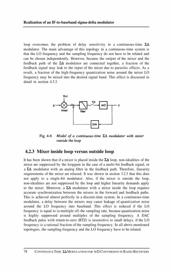
Realization of an IF-to-baseband sigma-delta modulator
loop overcomes the problem of delay sensitivity in a continuous-timemodulator. The main advantage of this topology in a continuous-time system isthat the LO frequency and the sampling frequency do not have to be related andcan be chosen independently. However, because the output of the mixer and thefeedback path of the modulator are connected together, a fraction of thefeedback signal may leak to the input of the mixer due to parasitic effects. As aresult, a fraction of the high-frequency quantization noise around the mixer LOfrequency may be mixed into the desired signal band. This effect is discussed indetail in section 4.3.3.
4.2.3 Mixer inside loop versus outside loop
It has been shown that if a mixer is placed inside the loop, non-idealities of themixer are suppressed by the loopgain in the case of a multi-bit feedback signal, ora modulator with an analog filter in the feedback path. Therefore, linearityrequirements of the mixer are relaxed. It was shown in section 3.2.3 that this doesnot apply to a single-bit modulator. Also, if the mixer is outside the loop,non-idealities are not suppressed by the loop and higher linearity demands applyto the mixer. Moreover, a modulator with a mixer inside the loop requiresaccurate synchronization between the mixers in the forward and feedback paths.This is achieved almost perfectly in a discrete-time system. In a continuous-timemodulator, a delay between the mixers may cause leakage of quantization noisearound the LO frequency into baseband. This effect is reduced if the LOfrequency is equal to (a multiple of) the sampling rate, because quantization noiseis highly suppressed around multiples of the sampling frequency. A DACfeedback pulse with return-to-zero (RTZ) is insensitive to small delays, if the LOfrequency is a rational fraction of the sampling frequency. In all above mentionedtopologies, the sampling frequency and the LO frequency have to be related.
78 CONTINUOUS-TIME MODULATION FOR A/D CONVERSION IN RADIO RECEIVERS

4.3 IF mixer design
A mixer outside the loop avoids synchronization problems, and offers morefreedom of choice for the mixer LO frequency, which does not have to be relatedto the sampling frequency. The major advantage is that the choice for thesampling rate can be optimized for dynamic range performance and powerconsumption of the modulator, without affecting the LO frequency. Moreover,we have chosen to use a one-bit quantizer in the modulator for its highlinearity. Therefore, linearity of the mixer is not reduced when placed within the
loop. For these reasons, the IF-to-baseband modulator topology with themixer outside the loop is used for the design in this chapter.
4.3 IF mixer design
The design of the IF mixer is described in this section. An integrated design isshown of a passive mixer and an RC filter, which is optimized for high linearityperformance, low-power consumption, and integration with the continuous-timeloopfilter of a modulator. This mixer/filter implementation is used as the inputstage for the IF-to-baseband modulator. Furthermore, aspects of linearity,mixer driving and self-mixing as a result of charge injection are discussed.
4.3.1 Mixer topology
The passive mixer topology of Fig.4-7a, that is used for the design in this chapter,is built from resistors and transistor switches, performing the V/I conversion andfrequency translation, respectively. The transistor switches periodically coupleand cross-couple the input current signal. This way, the input signal withfrequency is multiplied by the rectangular LO waveform with frequency
CONTINUOUS-TIME MODULATION FOR A/D CONVERSION IN RADIO RECEIVERS 79
The (downconverted) fundamental output frequency of the mixer equals
For proper operation, the passive mixer is connected to the virtual ground nodesof an amplifier. Due to the high gain and the feedback, the input nodes of theopamp are virtual ground nodes. Because the opamp input nodes are modulatedby only a fraction of the input voltage, highly linear performance can be achieved.The conversion gain of this passive mixer is:

Realization of an IF-to-baseband sigma-delta modulator
where is the duty cycle of the LO signal. The voltage amplifier of Fig.4-7a canbe easily transformed into an RC filter, by replacing the feedback resistors withcapacitors (Fig.4-7b). This topology is a very suitable implementation for the IFinput stage of a continuous-time modulator with mixer [4.3]. The resistorsperform a linear V/I conversion of the input signal. The current signal is linearlymodulated by the mixer switches. As it has no bias current, the passive mixer doesnot add to the power consumption of the modulator. The virtual ground nodes ofthe amplifier provide linear summation nodes for the input current and the DACfeedback current in Fig.4-7b). Moreover, the virtual ground nodes offergood isolation of the LO signal and the feedback bitstream signal. Isolation isessential for an independent choice of the sampling frequency and LO frequency(section 4.3.3). In the next sections, the circuit of Fig.4-7b is analyzed in moredetail, regarding linearity, LO driving, and charge injection.
4.3.2 Linearity performance
In this section, the non-linearity of the passive mixer topology of Fig. 4-7b isanalyzed. It has been assumed that the input (Poly-Si) resistors are linear andthat the mixer switches are connected to ideal virtual ground nodes (opamp hasinfinite gain). For distortion analysis, a mixer transistor is modeled as a non-linearimpedance and an ideal switch (Fig. 4-8) [4.3]. The switch impedance iscalculated by
80 CONTINUOUS-TIME MODULATION FOR A/D CONVERSION IN RADIO RECEIVERS

4.3 IF mixer design
where is the current through the switch and the small-signal voltage acrossthe switch. Using the model of a MOS transistor operating in the linear region, theswitch impedance equals
where is the mobility, the oxide capacitance, W and L the transistordimensions, and is the effective gate-source voltage obeying
where is the threshold voltage. In this analysis it is assumed that isconstant. Having in mind that no bias current is flowing through the switchtransistor (only signal current) the signal voltage across the switch iscalculated using the small-signal parameter of Eq. (4-4),
where was given in section 3.2.3. Likewise, the signal current through theinput resistor and switch impedance can be calculated from Fig.4-8
Substituting Eq. (4-4), Eq. (4-6), and Eq. (4-7) gives a non-linear expression for thesignal current (after Taylor series expansion)
Using the result of Eq. (4-8), the expression for the third-order harmonicdistortion (for a sinusoidal input signal) is approximately
CONTINUOUS-TIME MODULATION FOR A/D CONVERSION IN RADIO RECEIVERS 81

Realization of an IF-to-baseband sigma-delta modulator
assuming that the switch impedance is much smaller than the input resistance.Inspecting Eq. (4-9) reveals that distortion can be minimized by applying a largeoverdrive voltage to the mixer switches. Furthermore, the switch impedancesshould be made small compared to the input resistance. This is achieved bymaking the W over L ratio of the switch transistors large. The upper limit of thetransistor size is determined by charge injection of the switches and speedrequirements
Example 4.1: Consider the following data; is 1 V (amplitude), is250 mV, is and is is 14 mV). Substituting theseparameters into Eq. (4-9) yields a HD3 of -107 dB. This example shows thathigh linearity of the mixer is achievable with this architecture.
4.3.3 Local oscillator driver
The mixer switches are connected to the input nodes of an opamp as well as to thefeedback paths of the sigma-delta modulator (Fig.4-7b). Being placed at the inputof the sigma-delta modulator, any non-idealities of the mixer will have a directimpact on the modulator performance. This also applies to the local oscillatorcircuit that drives the mixer. The mixer has two clock inputs and withcomplementary phases. Ideally, the clock signals have exactly 180 degrees phasedifference and infinitely steep rising and falling edges. However, due to parasiticeffects it is not possible to generate these perfect complementary clock signals.Assuming infinitely steep edges, four different phases can be distinguished incase the inverter that is generating signal has a small delay (Fig. 4-9). Duringphases and the clock signals are inverse to each other. During phasesand the clock signals are both high and low, respectively. If the mixer isimplemented with NMOS transistors, all switches are closed during phase andopen during phase The dual situation occurs if the mixer is implemented withPMOS devices. When all switches are conducting at the same time, a lowimpedance path connects the feedback paths of the sigma-delta modulator as wellas the input nodes of the opamp. In the following, two effects of the overlapping
CONTINUOUS-TIME MODULATION FOR A/D CONVERSION IN RADIO RECEIVERS82

4.3 IF mixer design
phases of the mixer clock are described. The first effect is due to the finitetransconductance of the opamp and the second one is due to the offset.
Effect of finite transconductance
To analyze the effect of the overlapping clock phase and the non-overlappingclock phase the DAC current flowing into the integration capacitors iscalculated during all phases using Fig.4-7b. It has been assumed that the inputvoltage is zero and that the amplifier does not have any offset. During phases
and one pair of switches is open and one is closed. The current inphases and equals
The right-hand term of the denominator can be neglected if the opamp has goodvirtual ground nodes (transconductance is high) and if the DAC resistance
and input resistance have values that are in the same order (term betweenbrackets in Eq. (4-10) is close to one). In phase all switches are conducting andan equivalent resistance (switch ON-impedance) is present between the inputnodes of the amplifier. The current in phase is
The term between the brackets is now much larger than one, if the DAC and inputresistances are large and the switch impedance small. Assuming that all mixerphases are within one DAC period does not change), the difference betweenEq. (4-10) and Eq. (4-11) represents the amplitude drop in DAC current during
CONTINUOUS-TIME MODULATION FOR A/D CONVERSION IN RADIO RECEIVERS 83

Realization of an IF-to-baseband sigma-delta modulator
phase Assuming that the input resistance is much larger than the switchimpedance and that the DAC resistance is much larger than the inverse of thetransconductance of the amplifier, the relative DAC current error is
amplifier is less sensitive to the low impedance of the mixer during phase Therelative charge error is calculated by
Example 4.2: Consider the following data: is 3.4 mA/V, is 70is is 200 ps, and is 10 MHz. From this data, it can be
84 CONTINUOUS-TIME MODULATION FOR A/D CONVERSION IN RADIO RECEIVERS
where is the interval time of phase and the local oscillator frequency. In
From Eq. (4-12) it can be seen that the larger the transconductance the smallerthe amplitude drop. In other words, with stronger virtual ground nodes the
phase all switches are open and the input resistors are disconnected from theopamp input nodes. The current can be simply determined from Eq. (4-10)considering that the input resistors have become infinitely large
The same analysis as before can be done to calculate the relative charge error inphase If is the interval time of phase the relative charge error is
In section 4.3.2 it has been shown that an important design constraint for linearityof the mixer is that
Comparing Eq. (4-13) and Eq. (4-15) shows that the charge error is much smallerin phase than in phase

4.3 IF mixer design
calculated that the relative charge errors are 0.045 % and 0.004 % in phaseand phase respectively. In this example the error in phase is about 40 dBsmaller than the error in phase
With the data of the example above, two different clock schemes have beensimulated. The first clock scheme has an overlapping and a non-overlappingphase (Fig.4-9) and the second scheme has two non-overlapping phases(Fig. 4-21). We refer to the clock schemes as overlapping and non-overlapping,respectively. Furthermore, the sampling frequency of the modulator is12.96 MHz and the local oscillator frequency is 6.48 MHz. The input signal is a6.531840 MHz sinusoidal, which is mixed down to 51.84 kHz by the 6.48 MHzmixer. The (non)-overlapping phases are all 200 ps. For both simulations, thehigh-frequency quantization noise spectrum is similar and Fig. 4-10 shows adetailed plot of this high-frequency quantization noise near the 6.48 MHz localoscillator carrier. Discrete tones are present at 6.368 MHz (-10.7 dB), 6.385 MHz(-10.8 dB), 6.420 MHz (-7.9 dB), 6.437 MHz (-7.9 dB), and 6.4717 MHz(-22.1 dB).
Fig. 4-11 shows the simulated low-frequency output spectrum of themodulator with mixer that is driven by the overlapping clock scheme. The signalcarrier is visible at 51.84 kHz and tones show up at 8.3 kHz (-92.9 dB), 43.5 kHz(-78.7 dB), 60.1 kHz (-78.6 dB), 95.4 kHz (-81.2 dB), and 112.0 kHz (-81.7 dB).The noise level gradually increases from about -120 dB to -110 dB (resolution
CONTINUOUS-TIME MODULATION FOR A/D CONVERSION IN RADIO RECEIVERS 85

Realization of an IF-to-baseband sigma-delta modulator
bandwidth is 129.6 Hz). The in-band noise and frequency tones are mainlyhigh-frequency quantization noise which is leaked in the signal band due to theoverlapping (and non-overlapping) phases of the LO mixer driver.
The output spectrum of the modulator with mixer, driven by thenon-overlapping clock scheme, is shown in Fig. 4-12. Two small tones around thesignal carrier can be observed at 44.5 kHz (-119.2 dB) and at 59.2 kHz(-118.8 dB). Again, these are high-frequency tones in the quantization noisespectrum at 6.48 MHz.
Consequently, in Fig.4-11 the high-frequency tones and noise leak into basebandwith a gain of -70.8 dB, which agrees with the result of Eq. (4-13). Thesignal-to-noise ratio within the frequency band from 1 kHz to 100 kHz is 39.3 dB.The suppression of the tones in Fig. 4-12 is simulated to be about 111 dB. TheSNR is 58.5dB, which is close to the SNR in the case of ideal complementaryclock phases (59dB). Compared to the simulation with overlapping clock signals,the resolution is improved more than 19 dB using a non-overlapping clockscheme.
86 CONTINUOUS-TIME MODULATION FOR A/D CONVERSION IN RADIO RECEIVERS
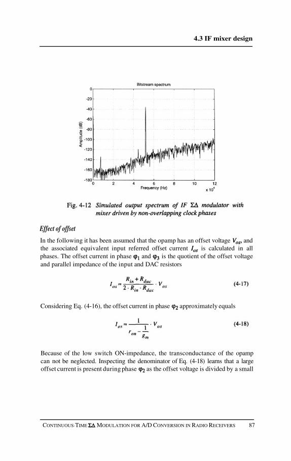
In the following it has been assumed that the opamp has an offset voltage andthe associated equivalent input referred offset current is calculated in allphases. The offset current in phase and is the quotient of the offset voltageand parallel impedance of the input and DAC resistors
Considering Eq. (4-16), the offset current in phase approximately equals
Because of the low switch ON-impedance, the transconductance of the opampcan not be neglected. Inspecting the denominator of Eq. (4-18) learns that a largeoffset current is present during phase as the offset voltage is divided by a small
4.3 IF mixer design
CONTINUOUS-TIME MODULATION FOR A/D CONVERSION IN RADIO RECEIVERS 87
Effect of offset

Realization of an IF-to-baseband sigma-delta modulator
impedance. In phase the input resistors are disconnected and the offset currentis derived from Eq. (4-17) considering that the input resistors are infinitely large
which is much smaller than the offset in phase because of the large DACimpedance.
Example 4.3: Using the data of the previous example and if is 3 mV andis the offset currents are calculated to be and 45.5 nA in
phase and phase respectively. The equivalent offset current can becalculated by multiplying Eq. (4-18) and Eq. (4-19) with the duty cycle of theoverlapping and non-overlapping phase respectively.
4.3.4 Self-mixing
Clock feedthrough of the LO signal to the input of the mixer may result in anoffset at the output of the mixer. This effect is referred to as self-mixing [4.4] andwill be explained in this section. The gate capacitors of a MOSFET switchprovide high frequency paths for the LO signal. The model of a switch includingparasitic gate-capacitors is shown in Fig. 4-13, where and are thegate-drain and gate-source capacitances respectively [4.5]. If the LO signal at thegates of the switches changes from low to high, or vice versa, charge istransferred to the input and output nodes of the mixer.
With the model of Fig.4-14 the self-mixing mechanism is explained. It isassumed that all switches are ideal is zero) and that perfect complementaryLO clock signals are used. Only the parasitic gate-capacitors of switch havebeen included. In Fig.4-14a the switches are turned on and are turnedoff. The thick line shows the charge transportation path. The charge through both
88 CONTINUOUS-TIME MODULATION FOR A/D CONVERSION IN RADIO RECEIVERS

4.3 IF mixer design
gate capacitors is pumped into the upper integration capacitor. The differentialoutput voltage step as a result of charge injection of switch is
where is the voltage swing at the gate of switch The other situation isshown in Fig.4-14b, where are switched off and are switched on.Now, the charge of the gate-source capacitor is pumped into the upper integrationcapacitor and the charge of the gate-drain capacitor is pumped into the lowerintegration capacitor through switch The output step equals
Adding Eq. (4-20) and Eq. (4-21) gives the output voltage after a mixingperiod, due to self-mixing
Hence, the charge transfer through the gate-source capacitor is balanced out afterone mixing period, while the charge of the gate-drain capacitor is modulated byswitches and resulting in an equivalent offset current flowing into theintegration capacitors.
CONTINUOUS-TIME MODULATION FOR A/D CONVERSION IN RADIO RECEIVERS 89

Realization of an IF-to-baseband sigma-delta modulator
To minimize the effect of self-mixing, good matching of parasitic capacitors ofthe switches is required. If the switches have identical impedances and parasiticcapacitors, all charge transfers are balanced and the offset is zero. To minimizecharge injection, the switches should have small dimensions in order to have littleparasitic capacitance. This design constraint is opposed to the linearity constraint,which requires switches with a large W/L ratio (section 4.3.2). To satisfy bothconstraints, the switches can be dimensioned best with a small channel length.
4.4 IF sigma-delta modulator design
In this section the design of a continuous-time modulator with mixer isdescribed for A/D conversion of input signals, which are modulated at anintermediate frequency. The main target of this design is to show that highlylinear A/D conversion of IF signals can be achieved at low-power consumption.The mixer is placed outside the loop. For high linearity of the DAC in thefeedback path, a single-bit modulator is used.
4.4.1 IF sigma-delta modulator topology
The block diagram of the modulator with mixer is shown in Fig. 4-15 [4.3].The fully differential modulator includes a mixer at the input, a fourth-ordercontinuous-time lowpass loopfilter [4.6] - [4.7], a single-bit A/D converter and afeedback path with D/A converter closing the loop. The input stage is thehighly linear RC integrator with mixer topology of Fig.4-7b. The higher-orderfilter stages are transconductance-C integrators. The feedforward paths areimplemented by means of transconductance amplifiers, which provide currentoutput signals. Summing of the currents can be done by simply connecting all theoutput nodes. The comparator is designed to have current input capability. Eachsampling period, the comparator takes a sample of the output signal of theloopfilter and determines the signal polarity. The output is a digital bitstream atthe sample rate. The output data is fed back through a D/A converter whichprovides a positive or negative reference voltage. The reference voltage isconverted into a current by the feedback resistors and subtracted from theinput current. The filter stability coefficients have been determined according tothe analysis in section 3.4.1. With a sampling rate of 13.0 MHz, which is acommon GSM crystal oscillator frequency, the oversampling factor is 48
90 CONTINUOUS-TIME MODULATION FOR A/D CONVERSION IN RADIO RECEIVERS

4.4 IF sigma-delta modulator design
CONTINUOUS-TIME MODULATION FOR A/D CONVERSION IN RADIO RECEIVERS 91

Realization of an IF-to-baseband sigma-delta modulator
With a fourth-order loopfilter, the (full signal) signal-to-quantization-noise in100 kHz bandwidth is simulated to be 88 dB. Fig. 4-16 shows the simulatedoutput spectrum of the fourth-order modulator. In this simulation, the LOfrequency is equal to half the sampling frequency (6.5 MHz) and the full-scale IFinput signal is at 6.510 MHz. In the following, the designs of the individualblocks are described in more detail.
4.4.2 Input filter stage design
In Fig.4-17 the circuit design of the differential opamp with its biasing circuit isshown, that is used for the input filter stage. The opamp has a telescopicarchitecture implying that all transistors, including the common-mode transistors,are stacked in only two differential branches [4.8]. This way, current consumptionof the opamp is a factor of two lower than of an opamp with a folded cascodearchitecture [4.9]. Due to the stacking of all transistors, the maximum outputswing is limited. The differential input pair together with the cascodetransistors boost the DC voltage gain of the differential input pair to avalue of about 80 dB. The current sources also have cascode transistors
in order to keep the output impedance high. Transistor is the PMOScurrent source of the opamp. Transistors are biased in the linear regionand the gates of these transistors control the common-mode output level, set bytransistor
92 CONTINUOUS-TIME MODULATION FOR A/D CONVERSION IN RADIO RECEIVERS

4.4 IF sigma-delta modulator design
The minimum supply voltage is determined by the saturation voltages ofand (200mV each), the drain-source voltage of (100mV), and the
maximum peak-to-peak swing at the output Taking into accountprocess spread, the minimum supply voltage is about 1.6 V. For proper biasing ofthe cascode transistors at full output swing, the output common-modelevel is designed to be lower than the input common-mode level
Distortion versus supply current
In this section an expression for the low-frequency distortion of the RC integratoris derived. Distortion of the opamp of Fig. 4-17 is mainly caused by the non-lineardifferential input transistor pair [4.10]. Fig.4-18 shows the non-linearmodel of the RC integrator in the loop. Due to the finite DC gain of theopamp, a small residue signal is modulating the non-linear input pair. Using thesquare-law model of a MOS transistor [4.11], the residue voltage can becalculated (strong inversion)
where is the output current, is the bias current of transistors L and Ware the transistor dimensions, and the mobility. Taylor series expansion ofEq. (4-23) yields an expression for the linear and non-linear transconductance.
CONTINUOUS-TIME MODULATION FOR A/D CONVERSION IN RADIO RECEIVERS 93

Realization of an IF-to-baseband sigma-delta modulator
Usually, in a differential system, the third-harmonic term is dominating thenon-linear transfer
where the transconductance equals
where is the effective gate-source voltage. With the non-lineartransconductance of Eq. (4-24) the relation between the linear residue currentand residue voltage (Fig. 4-17) of the integrator is
where equals
With Eq. (4-26), the expression for the residue voltage is approximated as afunction of the current
The expression for the residue voltage is known, and the non-linear expression forthe input current and the feedback current can be extracted as a function ofthe residue current
94 CONTINUOUS-TIME MODULATION FOR A/D CONVERSION IN RADIO RECEIVERS

4.4 IF sigma-delta modulator design
Using the result of section 3.2.3, the relation for the third harmonic distortion(HD3) is determined from Eq. (4-29)
To minimize the bias current the input resistance is designed to be as largeas possible. The upper limit for is set by the allowed thermal noise level(Eq. (4-31)). Moreover, the effective gate-source voltage of the inputtransistors should be made small (close to moderate inversion). This is done bydesigning the input transistors with a large W/L ratio. Table 4-1 shows the designparameters for the first integrator. Substituting these parameters into Eq. (4-30)gives an estimation of the third-harmonic distortion of the modulator, which isbelow -100dB.
The input resistors and feedback resistors are dimensioned such that their noisecontributions dominate quantization noise. The contribution of circuit noise of theopamp is neglected. In addition, due to the large signal bandwidth, thermal noiseof the resistors dominates flicker noise of the opamp. The thermal noise of theresistors is
The resistor ratio is determined by the maximum input level and theDAC reference level according to
CONTINUOUS-TIME MODULATION FOR A/D CONVERSION IN RADIO RECEIVERS 95

Realization of an IF-to-baseband sigma-delta modulator
where RTZ is the return-to-zero time (relative to the sampling period).Minimizing the resistor ratio value implies a small RTZ interval and a largereference level The upper limit of the input resistance is determined byEq. (4-31) and Eq. (4-32).
4.4.3 Transconductance-C integrator
The higher-order filter stages of the modulator are implemented astransconductance-C integrators. The integrators have voltage input and voltageoutput capability. Fig. 4-19 shows the circuit design of the transconductanceamplifier. The differential input pair convert the input voltage into acurrent. A degeneration resistor between the sources of the input transistorsincreases the linear input range of the amplifier. Noise and distortion of the higherorder integrators are not critical, as non-ideal behavior is suppressed by the gainof the previous stages. The output current flows into the integration capacitorbetween the output nodes of the amplifier. Because of the lack of feedback, theinput impedance of the amplifier is very large. Transistors are NMOScurrent sources with cascodes The common-mode output level iscontrolled by transistors as described in the previous section. The DCgain of all filter stages add to the total loopgain. Accordingly, the gain of eachstage does not have to be high and 40 dB is sufficient. The input pair does notneed cascode transistors for gain enhancement. The minimum supply voltage isequal to the saturation voltages of transistors and (200 mV each),the drain-source voltage of (100 mV), and the maximum peak-to-peak swingat the output and the maximum peak-to-peak swing at the source of (both400 mV with 180° phase difference). Taking into account an extra 100 mV ofspread, gives a minimum supply voltage of 2 V. The critical part in the design ofthe OTA is the biasing of the input transistors Due to the sourcedegeneration, the full input swing at the gates of the input pair modulates thesources. As a number of transconductance-C integrators are cascaded, allintegrators are biased at equal input and output common-mode levels aswell as equal maximum input and output signal swings
96 CONTINUOUS-TIME MODULATION FOR A/D CONVERSION IN RADIO RECEIVERS

4.4 IF sigma-delta modulator design
4.4.4 A/D and D/A converter
The one-bit A/D converter design is shown in Fig. 4-20. It has a differentialcurrent input which is converted into a voltage output by the latch withcascode transistors to increase latching speed. The latch is biased bycurrent sources with cascodes The output swing of the latchhas been limited by diodes to ensure proper biasing of the NMOS currentsources and cascode transistors at full output swing of the latch. The latch outputsignal is fed into an inverter stage, producing a true digital output, which isstored into a flipflop. After the latch has made a decision, the latch output is resetto half the supply voltage by the CMOS switch If a mismatch existsbetween the capacitive loads of the differential output nodes of the latch,asymmetrical charge injection by the reset switch causes an offset. Due to thisoffset, the latch could be making incorrect decisions in the case of small inputsignals. However, these errors are not very critical as they are suppressed by thefourth-order loopfilter. The D/A converter consists of three switches, whichconnect the feedback resistors to the positive or negative reference, or a zeroreference during the return-to-zero time. Because the feedback signal is asingle-bit rectangular waveform, linearity of the DAC switches is not importantand they can have small dimensions. Care is taken that both the positive andnegative differential current pulses contain the same amount of charge.
CONTINUOUS-TIME MODULATION FOR A/D CONVERSION IN RADIO RECEIVERS 97
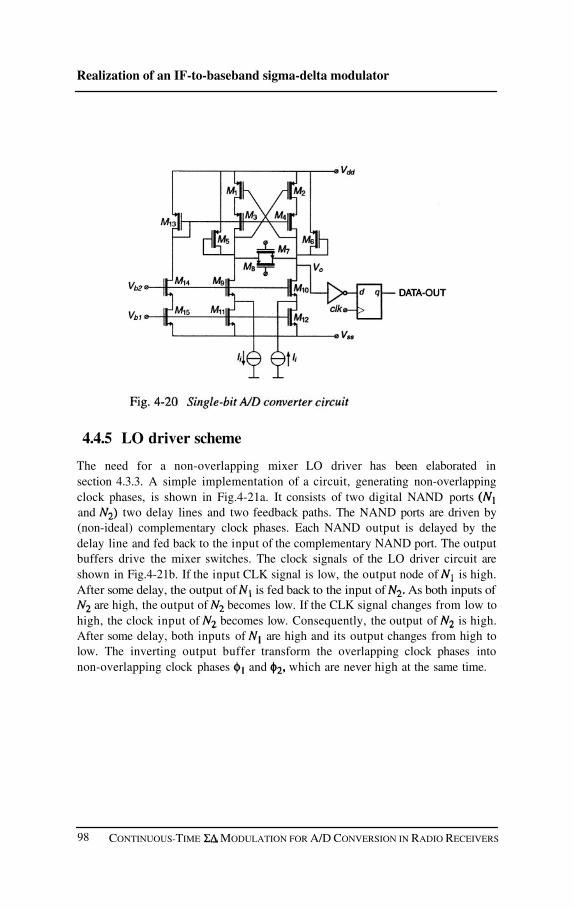
Realization of an IF-to-baseband sigma-delta modulator
4.4.5 LO driver scheme
The need for a non-overlapping mixer LO driver has been elaborated insection 4.3.3. A simple implementation of a circuit, generating non-overlappingclock phases, is shown in Fig.4-21a. It consists of two digital NAND portsand two delay lines and two feedback paths. The NAND ports are driven by(non-ideal) complementary clock phases. Each NAND output is delayed by thedelay line and fed back to the input of the complementary NAND port. The outputbuffers drive the mixer switches. The clock signals of the LO driver circuit areshown in Fig.4-21b. If the input CLK signal is low, the output node of is high.After some delay, the output of is fed back to the input of As both inputs of
are high, the output of becomes low. If the CLK signal changes from low tohigh, the clock input of becomes low. Consequently, the output of is high.After some delay, both inputs of are high and its output changes from high tolow. The inverting output buffer transform the overlapping clock phases intonon-overlapping clock phases and which are never high at the same time.
CONTINUOUS-TIME MODULATION FOR A/D CONVERSION IN RADIO RECEIVERS98

4.5 Experimental results
4.5 Experimental results
In this section the experimental results of two test chips are presented. The firsttest chip incorporates the fourth-order continuous-time modulator, without theIF mixer. The second test chip is the IF-to-baseband modulator of Fig.4-15.The chip micrograph (active area) and partitioning of the modulator withmixer is shown in Fig. 4-22. The input stage and its biasing circuit roughly takes50% of the total active area. The mixer area occupies only a very small part of thechip. The circuit has been designed in a 0.35 µm CMOS process with a singlepolysilicon layer, used for the resistors, and 5 metal layers. The active area of thetest chip measures The LO driver circuit has not been integrated on chipfor testing possibilities with different LO clock schemes.
CONTINUOUS-TIME MODULATION FOR A/D CONVERSION IN RADIO RECEIVERS 99

Realization of an IF-to-baseband sigma-delta modulator
4.5.1 Test chip 1: Baseband sigma-delta modulator
Fig.4-23 shows the measurement setup for the test chip. A Rohde&Schwarzaudio analyzer provides a floating differential voltage signal which is connectedto the input nodes of the chip. The bitstream output is connected to a 1-bit audioD/A converter which is synchronized with the master clock of the test chip. Theanalog DAC output is connected to the analog input of the Rohde&Schwarzanalyzer, performing an 8192 points Fourier transform. Due to the 75 kHzbandwidth of the audio DAC, the end-of-the-band noise spectrum of the chipoutput signal is slightly suppressed. In all measurement plots, the maximum inputlevel has been normalized to 0 dB. Signals and distortion tones, as well as noiseare all relative to 0 dB. The analyzer bandwidth is 100 kHz, and the resolutionbandwidth of the 8192 FFT is 12.2 Hz. All measurements have been done at asupply voltage of 2.5 V and a sampling rate of 13.0 MHz.
Distortion is measured with a full scale input signal. Fig. 4-24 shows the outputspectrum of a 0 dB, 10 kHz input signal. The second and third-harmonic tonescan be found at 20 kHz and 30 kHz respectively. Obviously, the second-harmonicis dominant at -90 dB, while the third-harmonic is well below -100 dB. It can beobserved that the noise band around the 10 kHz carrier is slightly suppressed. Dueto the limited dynamic range of the frequency analyzer, the signal carrier (and asmall frequency band around it) has been filtered out, before calculating the FFT.A gain correction of the signal carrier is done afterwards. The noise reductionaround the signal carrier has not been compensated and a small dip in the noiseremains. Domination of the second-harmonic tone is not to be expected in a fullydifferential circuit. A possible cause may be an unbalance between the differentialpaths, which results in a finite suppression of even harmonic distortion in thedifferential circuit. The low third-harmonic tone shows the excellent linearity ofthe modulator which was to be expected from the linearity analysis insection 4.4.2.
100 CONTINUOUS-TIME MODULATION FOR A/D CONVERSION IN RADIO RECEIVERS

4.5 Experimental results
CONTINUOUS-TIME MODULATION FOR A/D CONVERSION IN RADIO RECEIVERS 101

Realization of an IF-to-baseband sigma-delta modulator
Spectral tones are measured when no signal is applied to the input (section 3.2.2).The output spectrum is shown in Fig.4-25. A tone of -90 dB is present at 1.6 kHz,and a smaller one at 4.8 kHz (-100 dB).
The signal-to-noise-and-distortion (SINAD) ratio has been measured as afunction of the applied input level in Fig.4-26. The input frequency is 10 kHz andthe input level step size is 1 dB. From the SINAD plot, it can be seen that thecurvature is almost flat up to the full scale input level. For small input signals thedynamic range is about 88 dB. For a maximum input level, the peak SINAD ratiodrops to 86 dB, due to the second-harmonic distortion component and theincrement of quantization noise. For signals larger than 0 dB the modulator isoverloaded. Clipping of the integrators force the modulator into a stablesecond-order topology. If the modulator is in overload, large in-band distortiontones degrade the performance, and the SINAD ratio drops rapidly. At the end ofthe 100 kHz band, the quantization noise rolls off a little due to the filtering by theD/A converter in the measurement setup.
4.5.2 Test chip 2: IF-to-baseband sigma-delta modulator
The second test chip incorporates the modulator and the mixer. An FMgenerator was used to provide the IF input signal. The gain of the passive mixer is-3.9 dB. In order to have the same maximum input level as the baseband test chip,
102 CONTINUOUS-TIME MODULATION FOR A/D CONVERSION IN RADIO RECEIVERS
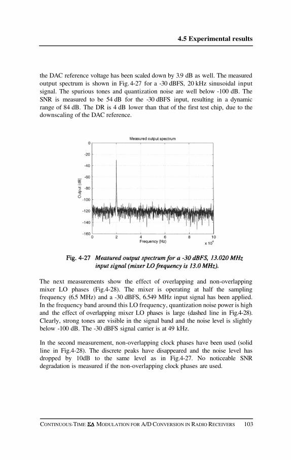
4.5 Experimental results
the DAC reference voltage has been scaled down by 3.9 dB as well. The measuredoutput spectrum is shown in Fig. 4-27 for a -30 dBFS, 20 kHz sinusoidal inputsignal. The spurious tones and quantization noise are well below -100 dB. TheSNR is measured to be 54 dB for the -30 dBFS input, resulting in a dynamicrange of 84 dB. The DR is 4 dB lower than that of the first test chip, due to thedownscaling of the DAC reference.
The next measurements show the effect of overlapping and non-overlappingmixer LO phases (Fig.4-28). The mixer is operating at half the samplingfrequency (6.5 MHz) and a -30 dBFS, 6.549 MHz input signal has been applied.In the frequency band around this LO frequency, quantization noise power is highand the effect of overlapping mixer LO phases is large (dashed line in Fig.4-28).Clearly, strong tones are visible in the signal band and the noise level is slightlybelow -100 dB. The -30 dBFS signal carrier is at 49 kHz.
In the second measurement, non-overlapping clock phases have been used (solidline in Fig.4-28). The discrete peaks have disappeared and the noise level hasdropped by 10dB to the same level as in Fig.4-27. No noticeable SNRdegradation is measured if the non-overlapping clock phases are used.
103CONTINUOUS-TIME : MODULATION FOR A/D CONVERSION IN RADIO RECEIVERS

Realization of an IF-to-baseband sigma-delta modulator
104 CONTINUOUS-TIME MODULATION FOR A/D CONVERSION IN RADIO RECEIVERS

4.5 Experimental results
Finally, linearity performance of the IF modulator is investigated. Two IFinput signals of -6 dBFS at 13.040 MHz and 13.052 MHz have been applied andthe mixer LO frequency is 13.0 MHz. As the two-tone signal generator alreadyproduces large inherent intermodulation distortion, two separate generators havebeen used, each generating a single tone. A linear signal combiner circuit hasbeen designed which combines both tones and produces a differential two-tone IFoutput signal with low intermodulation distortion. Fig. 4-29 shows the measuredoutput spectrum. The average of 8 consecutive measured spectra has beencalculated to get a clear view of the distortion tones. The -6 dBFS input tones aremodulated by the mixer to 40 kHz and 52 kHz respectively. Third-orderintermodulation distortion tones can be found at 28 kHz and 64 kHz respectivelyand are 84 dB down relative to the signal carriers. This results in a measured IM3of -84 dB. The noise bulb around the 40 kHz carrier is phase noise from the13.040 MHz signal generator. The generator producing the 13.052 MHz tone didhave a clean spectrum around the carrier. Switching of the generator frequenciesshowed a clean spectrum around the 40 kHz carrier and phase noise around the52 kHz carrier. The noise level of the spectrum of Fig.4-29 is higher than inFig. 4-27 (same resolution bandwidth). This observation is associated with thelimited dynamic range of the measurement system, as has been the case for thedistortion measurement of Fig. 4-24. For the single tone measurement ofFig. 4-24, this problem is solved by filtering out the signal carrier, beforeperforming the FFT. The problem remains for the two-tone measurement ofFig.4-29, because only one of the tones could be filtered out by the frequencyanalyzer. Therefore, at a full scale two-tone measurement, dynamic range islimited by the analyzer.
4.5.3 Performance summary
The measured performance has been summarized in Table 4-2. Total powerconsumption of the modulator and mixer is 1.8 mW from a 2.5 V supplyvoltage. From 50 samples, 49 chips were tested to be functional. The samplingfrequency of 13.0 MHz has been extracted from a GSM crystal oscillator. Theoscillator and phase-locked-loop (PLL) have a total measured phase jitter of4.5 ps.
CONTINUOUS-TIME MODULATION FOR A/D CONVERSION IN RADIO RECEIVERS 105

Realization of an IF-to-baseband sigma-delta modulator
4.6 Conclusions
In this chapter, the theory and design of a continuous-time modulator withintegrated mixer have been described. Frequency translation can be performedinside or outside the loop. Placing mixers inside the loop for frequencytranslation, gives suppression of mixer non-idealities by the loopgain, if themodulator has a multi-bit feedback signal or a filter in the feedback path. Phaseerrors between mixers inside a continuous-time loop cause synchronizationproblems which result in quantization noise modulation with the mixer LOfrequency. To overcome this problem the LO frequency and sampling frequencyshould be related. If frequency translation is done outside the loop, only asingle mixer is required which does not have the problem of synchronizationerrors. As a result, the LO frequency and sampling frequency can be chosenindependently.
It is shown that a passive mixer can be integrated with the RC integrator of theloopfilter for linear frequency translation. The RC filter has resistors for linear V/Iconversion of the input and feedback voltage signals. The virtual ground nodes ofan amplifier provide linear summation nodes of the signal currents. The passivemixer should be driven by a non-overlapping clock scheme to prevent modulation
106 CONTINUOUS-TIME MODULATION FOR A/D CONVERSION IN RADIO RECEIVERS
4.6 Conclusions
of the quantization noise spectrum with the LO frequency, by periodic shorting ofthe differential feedback paths.
Measurement results of a prototype test chip with the integrated design of afourth-order continuous-time modulator and passive mixer topology show thathigh linearity of the mixer is achieved. Power consumption of the mixer isnegligible. Driving the mixer with an overlapping clock scheme showed seriousperformance degradation for an LO frequency equal to half the samplingfrequency. This effect of quantization noise modulation with the LO frequency isgreatly suppressed if the mixer is driven with a non-overlapping clock scheme.The IF-to-baseband A/D converter realizes 82 dB of dynamic range in 100 kHz ata power consumption of only 1.8 mW. Measured third-order intermodulationdistortion (IM3) for two -6 dBV input tones is -84 dB.
CONTINUOUS-TIME MODULATION FOR A/D CONVERSION IN RADIO RECEIVERS 107

Realization of an IF-to-baseband sigma-delta modulator
References
[4.1] Namdar A., and B.H. Leung, “A 400-MHz, 12 bit, 18-mW, IFDigitizer with Mixer Inside a Sigma-Delta Modulator Loop,” IEEEJ. Solid-State Circuits, pp. 1765-1776, Dec. 1999.
[4.2] Song, B.S., “A Fourth-order Bandpass Delta-Sigma Modulator withReduced Number of Op Amps,” IEEE J. Solid-State Circuits, pp.1309-1315, Dec. 1995.
[4.3] Breems, L.J., E.J. van der Zwan, and J.H. Huijsing, “A 1.8-mWCMOS Modulator with Integrated Mixer for A/D Conversion ofIF Signals,” IEEE J. Solid-State Circuits, vol. pp. 468-475, Apr.2000.
[4.4] Abidi, A.A., “Direct-conversion radio transceivers for digitalcommunications,” IEEE J. Solid-State Circuits, vol. 30, pp.1399-1410, Dec. 1995.
[4.5]
[4.6]
[4.7]
[4.8]
[4.9]
[4.10]
[4.11]
Gregorian, R., G.C. Temes, Analog MOS integrated circuits forsignal processing; design, manufacturing, and applications, JohnWiley & Sons, New York, 1986.Zwan, E.J. van der, “A 2.3 mW CMOS Modulator for AudioApplications,” ISSCC Dig. Tech. Papers, pp. 220-221, Feb. 1997.Breems, L. J., E. J. van der Zwan and J. H. Huijsing, “A 1.8 mWCMOS Modulator for Mobile Communication,” Proc. ofWorkshop on Circuits, Systems and Signal Processing, pp. 61-64,Nov. 1998.Nicollini, G., F. Moretti, M. Conti, “High-frequency fullydifferential filter using operational amplifiers withoutcommon-mode feedback,” IEEE J. Solid-State Circuits, pp.803-813, Jun. 1989.Huijsing, J.H., Operational amplifiers; Theory and design, KluwerAcademic Publishers, Boston, 2001.Breems, L. J., E. J. van der Zwan and J. H. Huijsing, “Design forOptimum Performance-to-Power Relation of a Continuous-TimeModulator,” Proc. of ESSCIRC, pp. 318-321, Sep. 1999.Tsividis, Y.P., Operation and modeling of the MOS transistor,McGraw-Hill, New York, 1987.
108 CONTINUOUS-TIME MODULATION FOR A/D CONVERSION IN RADIO RECEIVERS

Realization of aquadrature sigma-deltamodulator
5.1 Introduction
In this chapter the design of a quadrature modulator with dynamic elementmatching circuit for image rejection improvement is presented. This A/Dconverter has been designed for application in an AM/FM radio receiver. Inchapter 2 it was explained that image rejection performance in a receiver withfrequency translation of the desired channel to a low-IF should be in the order of80-90 dB. This amount of image rejection is achieved with a combination ofchannel selection and quadrature mixing. In this chapter, the image rejectionperformance of a quadrature IF-to-baseband modulator will be analyzed. Insection 5.2 the main limitations of image rejection in the quadraturemodulator are shown. A powerful way to improve matching and image rejectionis DEM. In section 5.3.1 a DEM algorithm is presented which is controlled by thecomplex bitstream output of the quadrature modulator. The implementation ofthe DEM circuit is shown in section 5.3.2 and the effect of impedance mismatchand charge injection of the DAC and DEM switches are explained in section 5.3.3and section 5.3.4 respectively. In section 5.4 the design of a prototype test chip isshown, and experimental results of the realized chip can be found in section 5.5.Finally, conclusions have been drawn in section 5.6.
CONTINUOUS-TIME MODULATION FOR A/D CONVERSION IN RADIO RECEIVERS 109
5

Realization of a quadrature sigma-delta modulator
5.2 Image interference
The design of the quadrature modulator in this chapter consists of two IF-to-baseband modulators as presented in chapter 4. The mixers of the modulatorsare driven by quadrature LO clock signals, to generate quadrature input signalswith 90° phase difference. In section 2.4.3 it was explained that any gain or phasemismatch between the quadrature signals becomes evident in a finite imagerejection ratio. In a modulator, non-idealities at the input of the systemdominate the overall performance (section 3.2.3). Errors which are introducedfurther in the loop, are reduced by the gain of the preceding stages. This alsoapplies to gain and phase mismatch between the I and Q signals in a quadrature
modulator system. Fig. 5-1 shows a general model of a quadraturemodulator. The input signal X is fed to the quadrature paths, which bothincorporate a V/I converter and current mixer, producing quadrature signalsand The quadrature loopfilter may consist of two real filters or a complexfilter (section 3.5.2). Two sampling comparators generate the quadrature single-bit datastreams DATA-I and DATA-Q. The digital output is fed to the feedbackloop that has a DAC and a V/I converter. Depending on the logic level of the DACinput signal, that can be a logic ‘1’ or ‘0’, the output of the DAC is eitherconnected to the positive reference voltage or negative reference voltage
respectively. The DAC output voltage is converted into a current by a V/Iconverter and subtracted as a current signal from the input current signal.
110 CONTINUOUS-TIME MODULATION FOR A/D CONVERSION IN RADIO RECEIVERS

5.3 Dynamic element matching
If it is assumed that ideal subtraction of the input and feedback signals isperformed in the system of Fig. 5-1, the maximum image rejection ratio is limitedmainly due to
Mismatch between D/A converters
Mismatch between mixers and quadrature LO signals
Mismatch between V/I converters
In the implementation of the quadrature modulator of Fig. 5-1, the mixers andDACs consist of switches. Mismatch between the switches is negligible if theswitch impedance is much smaller than the impedance of the V/I converters.Accurate phase matching between the quadrature LO signals is achieved by re-clocking these signals with a four times higher master clock [5.1]. The V/Iconverters have been implemented with polysilicon resistors. These resistorsexhibit a parasitic capacitance to the underlying layer, and add a phase shift to theinput and feedback signals. The V/I converters in the input paths are outside the
loop, and a phase shift of the input signal does not affect stability. Therefore,the resistors can be designed with large dimensions (having large parasiticcapacitance) for good matching. Moreover, as the signals through these V/Iconverters in the quadrature paths are identical, (matched) capacitive coupling ofthe signals from the I to the Q path (and vice versa) is not a problem. As aconsequence, the resistors of both V/I converters can be placed in an interleavedconfiguration to improve matching. This does not apply to the V/I converters inthe feedback paths. For stability of the loop, the parasitic delay of the resistors inthe feedback circuit must be small. Therefore, small-sized resistors are required.Furthermore, parasitic coupling between the feedback paths adds to the totalimage interference of the quadrature modulator. Hence the feedback resistors ofthe I and Q paths should be placed in isolation from each other. Consequently,matching of the feedback resistors is less optimized than matching of the inputresistors.
5.3 Dynamic element matching
To improve matching of the feedback resistors, dynamic element matching isused which is described in this section. Dynamic element matching is based onperiodic exchanging of reference elements which may have a mismatch. As aresult, the mismatch is modulated with the exchange rate to another (out-of-band)frequency. It was explained in the previous section that the V/I converters in thefeedback paths are implemented with small-sized resistors that do not have very
CONTINUOUS-TIME MODULATION FOR A/D CONVERSION IN RADIO RECEIVERS 111

Realization of a quadrature sigma-delta modulator
good matching. Therefore, in this section, different DEM algorithms are exploredto improve the matching between the quadrature feedback paths of themodulator of Fig. 5-1. In all simulations in this section, a quadrature loopfilterwith 5 complex integrators is used, having the same NTF as was shown inFig. 3-34, with all notches being placed in the positive frequency band. Theoutput spectrum of this modulator, in the case of ideal matching between thequadrature paths, was already shown in Fig. 3-36.
A gain mismatch between the V/I converters (and the DACs) in the quadraturefeedback paths can be modeled by adding an extra gain block in both paths(Fig. 5-2). It is assumed that, except for these gain blocks, the other functionalblocks in the quadrature modulator are perfectly matched. Due to a gainmismatch, the amplitude of the analog feedback signal in the I-path issomewhat larger (or smaller) than the amplitude of the analog feedback signal inthe Q-path In this section it is assumed that the normalized gain in the I-pathis and that normalized gain in the Q-path is where is the relativemismatch factor. In the time domain, the output signal of the quadraturemodulator of Fig. 5-2 can be approximated by
112 CONTINUOUS-TIME MODULATION FOR A/D CONVERSION IN RADIO RECEIVERS

5.3 Dynamic element matching
where I and Q are the bitstream outputs of the I and Q modulators respectively,and the terms with are the error signals. Rearranging Eq. (5-1) gives
where the first term (I+jQ) is the (desired) output signal of a quadraturemodulator (without mismatch) and the second term between brackets isthe error signal (E) due to the gain mismatch Comparing both expressions inEq. (5-2) reveals that the error signal of the Q modulator has an opposite sign inrespect to its desired output signal. In the frequency domain this means that the(desired) output signal spectrum and the error spectrum (image) are mirroredaround DC. In other words, a part of the negative frequency band ‘leaks’ into thepositive frequency band (and vice versa). This is the essence of imageinterference.
The effect of a gain mismatch between the feedback signals is simulated and theresult is shown in Fig. 5-3. The desired signal band ranges from DC to
where is the sampling frequency, while the image band is in thenegative frequency plane, ranging from DC to An input signal is
CONTINUOUS-TIME MODULATION FOR A/D CONVERSION IN RADIO RECEIVERS 113

Realization of a quadrature sigma-delta modulator
applied in the (negative) image band at rad/s. The quadrature feedbackpaths have a gain mismatch of 0.1 % Due to the mismatch a signaloccurs at rad/s. The simulated image rejection ratio is 66 dB (Fig. 5-3)which was expected from Eq. (2-4). Also, some quantization noise from the imageband has leaked into the signal band (and vice versa) due to the finite amount ofimage suppression (section 3.5.2). Hence, mismatch between the feedbacksignals of a quadrature modulator causes leakage of noise and signals in the(negative) image band to the (positive) desired signal band (and vice versa).
Fig. 5-4 shows the model of the quadrature modulator with a DEM circuit.The DEM circuit consists of choppers at both sides of the quadrature feedbackpaths. The choppers consists of two pairs of switches that either couple or cross-couple the quadrature feedback paths. Thus, the feedback paths with the gainmismatch can be exchanged by the DEM choppers. If the DEM control signal
is high (logic ‘1’) the feedback paths are coupled straight through. Ifis low (logic ‘0’) the feedback paths are cross-coupled. In this way, the gainmismatch is modulated by the DEM control signal and the average gains ofboth DACs can be dynamically matched. A simple choice for the control signal ofthe DEM switches is a 50% duty cycle clock with a fixed frequency
Fig. 5-5 shows the simulated output spectrum in the case of a 0.1% gainmismatch between the quadrature feedback signals and is
rad/s. As a result of the DEM, there is no ‘leaked’ image componentpresent at rad/s (as was the case in Fig. 5-3). This image signal is
114 CONTINUOUS-TIME MODULATION FOR A/D CONVERSION IN RADIO RECEIVERS
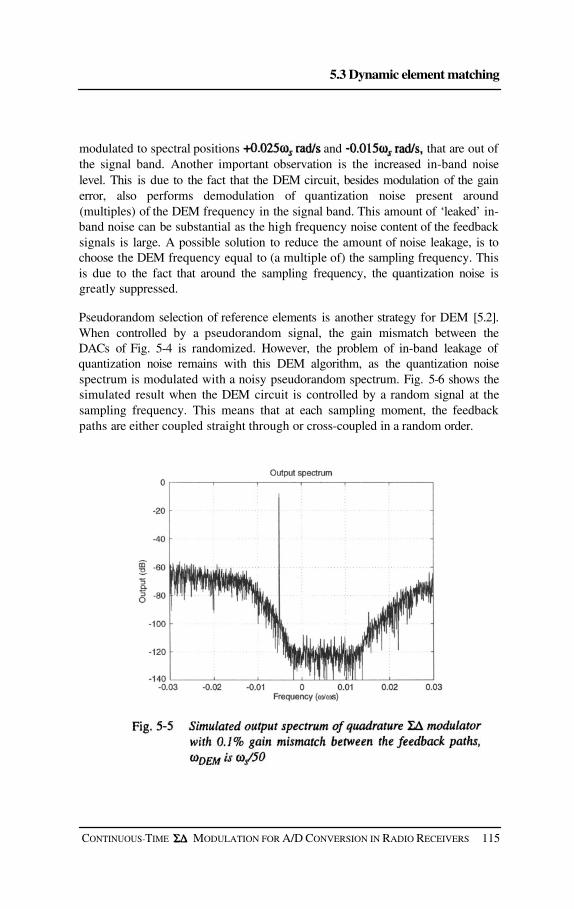
5.3 Dynamic element matching
modulated to spectral positions and that are out ofthe signal band. Another important observation is the increased in-band noiselevel. This is due to the fact that the DEM circuit, besides modulation of the gainerror, also performs demodulation of quantization noise present around(multiples) of the DEM frequency in the signal band. This amount of ‘leaked’ in-band noise can be substantial as the high frequency noise content of the feedbacksignals is large. A possible solution to reduce the amount of noise leakage, is tochoose the DEM frequency equal to (a multiple of) the sampling frequency. Thisis due to the fact that around the sampling frequency, the quantization noise isgreatly suppressed.
Pseudorandom selection of reference elements is another strategy for DEM [5.2].When controlled by a pseudorandom signal, the gain mismatch between theDACs of Fig. 5-4 is randomized. However, the problem of in-band leakage ofquantization noise remains with this DEM algorithm, as the quantization noisespectrum is modulated with a noisy pseudorandom spectrum. Fig. 5-6 shows thesimulated result when the DEM circuit is controlled by a random signal at thesampling frequency. This means that at each sampling moment, the feedbackpaths are either coupled straight through or cross-coupled in a random order.
CONTINUOUS-TIME MODULATION FOR A/D CONVERSION IN RADIO RECEIVERS 115

Realization of a quadrature sigma-delta modulator
In the next section, another dynamic element matching technique is presentedwhich is controlled by the complex bitstream output of the quadraturemodulator. The matching algorithm applies to both continuous-time and discrete-time modulators, with lowpass or bandpass filters. The main advantage of thisalgorithm is that it does not have the problem of quantization noise demodulation,as is the case for the traditional techniques which have been discussed before. Insection 5.3.1, the DEM algorithm is described in mathematical terms. The circuittopology is shown in section 5.3.2, and implementation related non-idealities,including impedance mismatch and charge injection of the DEM switches, arediscussed in section 5.3.3 and section 5.3.4 respectively.
116 CONTINUOUS-TIME MODULATION FOR A/D CONVERSION IN RADIO RECEIVERS

5.3 Dynamic element matching
5.3.1 Complex data-controlled DEM algorithm
The essence of the complex data-controlled DEM algorithm in this chapter is thatthe mismatch error spectrum E in Eq. (5-2) is mirrored relative to DC, withoutcausing demodulation of out-of-band quantization noise in the signal band.Mathematically, the following transformation is performed:
where is the transformation of the error signal E. In fact, the requiredtransformation holds sign inversion of the error signal of the Q modulatorReplacing the error term in Eq. (5-2) by yields
The signal spectrum and the transformed error signal spectrum are identical.Consequently, there is no leakage from the negative frequency band to thepositive frequency band (and vice versa) and perfect image rejection is obtained.To accomplish the required transformation of Eq. (5-3) it is considered that I andQ are single-bit bitstreams and switching between (normalized) levels +1 and -1.An important property is that the square of these bitstreams is always +1
Using this result, the transformation as shown in Eq. (5-3) can be realized bymodulation of the error signal E with the I and Q bitstreams [5.3]
Using the results of Eq. (5-5), Eq. (5-6) simplifies into
Indeed, Eq. (5-6) gives the required transformation of the error signal as defined inEq. (5-3). It should be noted that, due to the transformation of Eq. (5-6), the phaseof the gain error has been shifted by 270° (-j). However, this does not affectimage rejection as this phase shift is equal for both the I and Q modulators. In thenext section, the implementation of the DEM algorithm of Eq. (5-6) is shown.
CONTINUOUS-TIME MODULATION FOR A/D CONVERSION IN RADIO RECEIVERS 117

Realization of a quadrature sigma-delta modulator
5.3.2 DEM implementation
In the previous section, a mathematical derivation was given of a dynamicelement matching algorithm for the feedback paths of a quadrature modulator.The DEM algorithm is based on modulation of the mismatch between thefeedback paths by the product of the digital outputs of the I and Q modulators(Eq. (5-6)). In this section the practical implementation of this algorithm is shown.Fig. 5-7a. shows an example of the bitstream signals I and Q in the time domain.At sample moment the bitstream signals I and Q are equal.Therefore, the product of the bitstreams I·Q is positive (+1) and, according toEq. (5-6), the error E and the transformed error have the same sign. At samplemoment the bitstream signals I and Q are not equal. In this case theproduct of both bitstreams is negative and the error E and the transformed error
have opposite signs. Fig. 5-7b shows the logical representation of thealgorithm, which is similar to an EXOR operation.
The quadrature modulator with the DEM circuit is shown in Fig. 5-8. Thedynamic element matching is performed by mixers at both sides of the feedbackpaths. The DEM signal that drives the mixers is generated by a digital EXORport. If the I and Q signals are not equal the output of the EXOR is high (logic‘1’), and the feedback paths are coupled straight through. If the I and Q signalsare equal, the output of the EXOR is low (logic ‘0’), and the feedback paths arecross-coupled. This way, the sign of the gain error in both quadrature paths ismodulated according to the algorithm of Eq. (5-6). The system of Fig. 5-8 withthe DEM circuit has been modeled and simulated. Again, the same loopfiltercharacteristic as in the previous simulations in this chapter has been used. Inaddition, a gain mismatch of 0.5% is applied between the feedback paths. InFig. 5-3, the simulated output spectrum was shown of this modulator, withoutDEM.
118 CONTINUOUS-TIME MODULATION FOR A/D CONVERSION IN RADIO RECEIVERS

5.3 Dynamic element matching
CONTINUOUS-TIME MODULATION FOR A/D CONVERSION IN RADIO RECEIVERS 119
Realization of a quadrature sigma-delta modulator
The simulated output spectrum of the quadrature modulator with DEM isshown in Fig. 5-9. Obviously, in contrast to the output spectrum of Fig. 5-3, noimage leakage is present. This shows that the DEM algorithm provides excellentgain mismatch correction. Moreover, no noise leakage from the negativefrequency plane into the positive plane can be observed from Fig. 5-9. It shouldbe noted that the same result is obtained if a phase mismatch were to be appliedbetween the quadrature feedback paths.
Besides a gain (or phase) error, there may be a difference in the offset of bothquadrature feedback paths. This occurs, for example, if the DACs in thequadrature feedback paths have different offset voltages. Fig. 5-10 shows themodel of the quadrature modulator (with DEM circuit) where the DACs in thequadrature paths have offset voltages
If the I and Q bitstreams are equal, the feedback paths are cross-coupled, whilethey are coupled straight through if both bitstreams are not equal. Consequently,the positive and negative offset voltages are added to the reference voltage of the Iand Q modulators respectively in the case of unequal bitstreams, and added to thereference voltage of the Q and I modulators respectively in the case of equalbitstreams. Hence, the sign of the offset voltage is modulated according to theDEM algorithm, introducing an error
Eq. (5-8) shows that the offset voltage is modulated both by the I and Qbitstreams. This error has a noisy spectrum, as high frequency noise in the Ibitstream is modulated with the high frequency noise in the Q bitstream.Therefore, due to the DEM circuit, an offset between the quadrature feedbackpaths causes in-band ‘leakage’ of high frequency quantization noise, whichdegrades SNR.
The effect of an offset in the quadrature modulator of Fig. 5-10 has beensimulated with an offset voltage equal to 0.1% of where is thereference voltage of the DACs. The simulated spectrum is shown in Fig. 5-11a.The simulation plot shows an increased noise level and tones in the signal band.Fig. 5-11b shows the spectrum of I·Q and clearly the noise and tones ofFig. 5-11b are present in the spectrum of Fig. 5-11 a, as was expected fromEq. (5-8). This simulation shows that, due to the DEM operation, different offsetvoltages in the quadrature feedback paths cause demodulation of high frequencyquantization noise into the baseband.
CONTINUOUS-TIME MODULATION FOR A/D CONVERSION IN RADIO RECEIVERS120

5.3 Dynamic element matching
CONTINUOUS-TIME MODULATION FOR A/D CONVERSION IN RADIO RECEIVERS 121
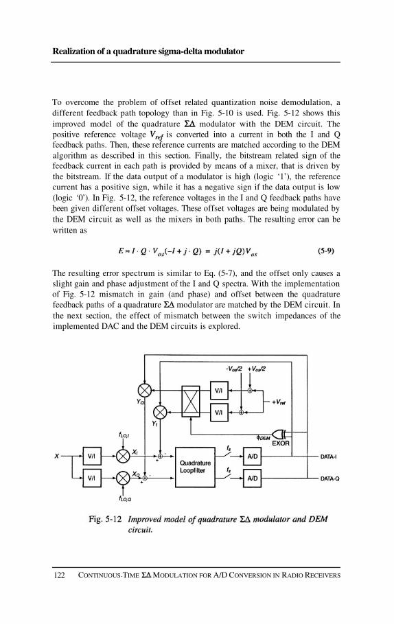
Realization of a quadrature sigma-delta modulator
To overcome the problem of offset related quantization noise demodulation, adifferent feedback path topology than in Fig. 5-10 is used. Fig. 5-12 shows thisimproved model of the quadrature modulator with the DEM circuit. Thepositive reference voltage is converted into a current in both the I and Qfeedback paths. Then, these reference currents are matched according to the DEMalgorithm as described in this section. Finally, the bitstream related sign of thefeedback current in each path is provided by means of a mixer, that is driven bythe bitstream. If the data output of a modulator is high (logic ‘1’), the referencecurrent has a positive sign, while it has a negative sign if the data output is low(logic ‘0’). In Fig. 5-12, the reference voltages in the I and Q feedback paths havebeen given different offset voltages. These offset voltages are being modulated bythe DEM circuit as well as the mixers in both paths. The resulting error can bewritten as
The resulting error spectrum is similar to Eq. (5-7), and the offset only causes aslight gain and phase adjustment of the I and Q spectra. With the implementationof Fig. 5-12 mismatch in gain (and phase) and offset between the quadraturefeedback paths of a quadrature modulator are matched by the DEM circuit. Inthe next section, the effect of mismatch between the switch impedances of theimplemented DAC and the DEM circuits is explored.
122 CONTINUOUS-TIME MODULATION FOR A/D CONVERSION IN RADIO RECEIVERS

5.3 Dynamic element matching
5.3.3 Impedance mismatch of DEM and DAC switches
In the design of chapter 4, the feedback of the loop incorporates a referencevoltage, DAC switches, and resistors as V/I converters, which are connected tothe input of the loopfilter. The error between the quadrature feedback signals inthe modulator is mainly due to mismatch of the DAC resistors. Fig. 5-13shows the differential implementation of the feedback circuit of Fig. 5-12. TheDAC resistors are connected to the positive and negative reference voltages. TheDEM switches interchange the DAC resistors. If the I and Q output bits are notequal, the resistors and are connected to the I-modulator, while theresistors and are connected to the Q-modulator. If the I and Qoutput bits are equal, the resistor pairs are interchanged and and areconnected to the Q-modulator, while and are connected to the I-modulator. Consequently, the mismatch between the DAC resistors is modulatedaccording to the complex data dependent DEM algorithm of section 5.3.1. TheDAC switches in the I and Q paths set the correct signs of the feedback signals.
To analyze the effect of impedance mismatch between the DAC switches, it isassumed that all switches of the DEM circuit are perfectly matched. Moreover,the DAC resistors are considered to be identical. Mismatch between theimpedances of the DAC switches is not modulated by the DEM circuit andintroduce a gain mismatch between the I and Q feedback signals. This gainmismatch is reduced by means of isolation and balancing. The amount of
CONTINUOUS-TIME MODULATION FOR A/D CONVERSION IN RADIO RECEIVERS 123
Realization of a quadrature sigma-delta modulator
isolation is calculated as the ratio between the switch impedance and DACresistance. The matching between the switches determines the balancing factor. Ifit is assumed that the switches in both DACs are perfectly matched, the gainmismatch between the feedback signals is calculated by
where is the average switch impedance and is the mismatch between theswitch impedances of the DACs in the I and Q paths. The first fraction of theright-hand side of Eq. (5-10) is the isolation factor and the second fraction is thebalancing factor.
Example 5.1: Consider is is and is the gainerror is 1E-3 (-60dB). With this gain error, the image rejection is 66dB.
Next, the effect of mismatch between the DEM switches is investigated. It hasbeen assumed that all DAC switches and DAC resistors are perfectly matched.The first situation is that the switches in the DEM-I circuit in the I path areidentical as well as the switches in the DEM-Q circuit in the Q path. A mismatchbetween the DEM-I and DEM-Q circuits (Fig. 5-14a) is similar to a mismatchbetween the DAC resistors and is compensated with the DEM algorithm. Thesecond situation is that the set of DEM switches which are driven by signal arematched, as well as the set of switches driven by In the case of a mismatchbetween the two sets of switches (Fig. 5-14b), the I and Q path are alwaysperfectly matched and no gain error is introduced. The third situation occurs if amismatch is present between the switches of the DEM-I and DEM-Q circuits, aswell as a mismatch between the switches driven by and Fig. 5-14c showsan example where there is a mismatch between the switches of DEM-I and DEM-Q, driven by which also have a mismatch between the matched switchesdriven by This way, an error is introduced which is modulated with the DEMalgorithm. This error is demodulated by the I and Q bitstreams that are driving theDAC switches. The resulting error between the I and Q feedback signals is
which consists of a gain adjustment of the signal and image spectra, as well asimage leakage. In case of a mismatch error of 0.1%, the image rejection is again66 dB. In conclusion, impedance mismatch between the switches of the DAC andDEM circuits can result in image leakage, which can be minimized by means of
124 CONTINUOUS-TIME MODULATION FOR A/D CONVERSION IN RADIO RECEIVERS

5.3 Dynamic element matching
isolation and balancing. Good isolation is obtained if the switch impedances aresmall compared to the DAC resistances, while balancing is optimized with thematching schemes of Fig. 5-14a or Fig. 5-14b.
5.3.4 Charge injection of DEM and DAC switches
The DAC switches as well as the DEM switches are connected to the virtualground nodes of the opamp of the first filter stage. This implementation is, like themixer (section 4.3.4) sensitive to asymmetric charge injection. First, the effect ofcharge injection of the DAC switches is analyzed. Fig. 5-15 shows theimplementation of the DAC with a parasitic gate capacitor of switch included.The other switches are supposed to be ideal, without parasitics. For simplicity,only a single modul tor is taken into account without DEM switches. Theswitches are NMOS transistors, which are closed at a high gate voltage and openat a low gate voltage. Suppose, all switches are open initially (gates are low). Ifswitches are closed and are opened, charge is injected through thegate capacitor of to the negative output node of the integrator. The outputvoltage is calculated by Eq. (4-20). If the switches are opened and are
CONTINUOUS-TIME MODULATION FOR A/D CONVERSION IN RADIO RECEIVERS 125
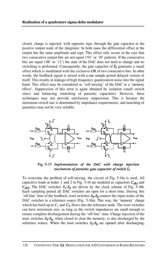
Realization of a quadrature sigma-delta modulator
closed, charge is injected, with opposite sign, through the gate capacitor to thepositive output node of the integrator. In both cases the differential offset at theoutput has the same amplitude and sign. This offset only occurs in the case thattwo consecutive output bits are not equal (‘01’ or ‘10’ pattern). If the consecutivebits are equal (‘00’ or ‘11’) the state of the DAC does not need to change and noswitching is performed. Consequently, the gate capacitor of generates a smalloffset which is modulated with the exclusive-OR of two consecutive bits. In otherwords, the feedback signal is mixed with a one sample period delayed version ofitself. This results in leakage of high frequency quantization noise into the signalband. This effect may be considered as ‘self-mixing’ of the DAC or a ‘memoryeffect’. Suppression of this error is again obtained by isolation (small switchsizes) and balancing (matching of parasitic capacitors). However, thesetechniques may not provide satisfactory suppression. This is because theminimum switch size is determined by impedance requirements, and matching ofparasitics may not be very reliable.
To overcome the problem of self-mixing, the circuit of Fig. 5-16a is used. Allcapacitive loads at nodes 1 and 2 in Fig. 5-16 are modeled as capacitors and
The DAC switches are driven by the clock scheme of Fig. 5-16b.Each sampling period all DAC switches are open for a short time. During this‘off-line’ time of the feedback, reset switches connect the input nodes of theDAC switches to a reference source (Fig. 5-16a). This way, the ‘memory’ chargewhich has built up in and flows into the reference node. The reset switchescan have minimum size, as long as the switch impedances are small enough toensure complete dischargement during the ‘off-line’ time. Charge injection of thereset switches when closed to clear the memory, is also discharged by thereference source. When the reset switches are opened after discharging,
126 CONTINUOUS-TIME MODULATION FOR A/D CONVERSION IN RADIO RECEIVERS

5.3 Dynamic element matching
another charge error is dumped into the memory capacitors through chargeinjection of the reset switches This error can be small because of theminimum size reset switches. The main advantage is that this error is identicaleach sampling period and only causes a small gain error of the feedback signal.The clock phases of the DAC switches and reset switches should be non-overlapping to prevent a short-circuit path between the input nodes of the opamp.In order not to interrupt the feedback signal, the reset switches should be activeduring the RTZ interval of the DAC.
So far, the DEM switches have not been taken into account. The DEM switchesalso suffer from charge injection and have the same problem of self-mixing. Thisproblem is solved again with the reset switches as shown in Fig. 5-16. If the DEMswitches are controlled during the reset time, charge that is injected by the DEMswitches flows into the reference node. Fig. 5-17 shows the completeimplementation of the quadrature DACs, the DEM circuit, and the reset switches,with the clock scheme. Initially, the I and Q bitstreams are 0 and 1 respectively.At sample moment the DAC switches in the I and Q paths are all switchedopen, and charge is injected into the capacitive loads of internal nodes 1-2 and 3-4. In the next sampling period, both bitstreams are 1 and the DEM circuit needs toexchange the DAC resistors. The DEM switches also dump charge into thecapacitive loads of the internal nodes. The capacitive loads are discharged by thereset switches. After the reset interval, the reset switches are all opened and dumpa small amount of charge into the ‘empty’ capacitive loads of the internal nodes.Each sampling period, this charge injection is identical and offset errors areintroduced at the input of the DAC-I and DAC-Q switches. This offset ismodulated with the I and Q bitstreams and only causes a small gain error betweenthe quadrature feedback signals.
CONTINUOUS-TIME MODULATION FOR A/D CONVERSION IN RADIO RECEIVERS 127

Realization of a quadrature sigma-delta modulator
Another parasitic capacitor between the drain and the source of the DACswitches, connects the input node of a DAC switch directly to the output.Fig. 5-18 shows the implementation of the DAC with two DEM switchesThe drain-source capacitance of and the parasitic gate capacitor of the DEMswitch are included. For independent analysis of the effect of the drain-sourcecapacitance, the total capacitive loads at nodes 1 and 2 are assumed to be equaland much larger than the drain-source capacitance. In the reset interval, switches
are all open, while switches are closed. If the state of the switcheschanges during reset time, charge is injected via the gate-source capacitance ofinto node 1. Via the drain-source capacitance of charge is transported to the
output of the integrator. The output voltage is calculated by
Where is the voltage swing at the gate of From Eq. (5-12) it can be learnedthat this is a second-order effect, as both fractions are much smaller than 1. Inaddition, this effect is compensated because nodes 1 and 2 are discharged by thereset switches and inject the same amount of charge with opposite sign.
128 CONTINUOUS-TIME MODULATION FOR A/D CONVERSION IN RADIO RECEIVERS

5.4 Quadrature sigma-delta modulator design
5.4 Quadrature sigma-delta modulator design
In this section the design of the quadrature modulator with the DEM circuit isdescribed for quadrature mixing and A/D conversion of IF input signals. Themain target of this design is to show that good matching of the quadraturefeedback signals can be achieved using the data dependent DEM algorithm aspresented in this chapter. The quadrature modulator consists of two IFmodulators (chapter 4), both with a loopfilter. The A/D converter isintended for low-IF conversion (section 2.2.1) in AM/FM radio receivers, with300 kHz bandwidth.
5.4.1 Topology
The A/D converter includes two fifth-order continuous-time modulators, withpassive mixers at the input. Fig. 5-19 shows the block diagram of one of themodulators. The mixers are driven by 10 MHz quadrature LO clocks with 90°phase difference. The sampling rate is 21.07 MHz, and the oversampling ratio ofthe modulator is 32. The fifth-order loopfilter has feedforward compensationpaths for high-frequency stability of the loop. Two local feedback paths createresonator stages with complex conjugate poles. With these resonators, gain can bedistributed equally within the signal band to minimize in-band quantization noise.The resonator notches are positioned at 165 kHz and 285 kHz respectively.
CONTINUOUS-TIME MODULATION FOR A/D CONVERSION IN RADIO RECEIVERS 129

Realization of a quadrature sigma-delta modulator
The simulated output spectrum of the quadrature modulator is shown inFig. 5-20 (signal at 100 kHz). The design of the feedforward compensatedlowpass filter with local feedback is described in section 3.4.2. Filter coefficientshave been dimensioned such that stability of the loop is preserved at 20% spreadin coefficient values. The reference voltage (2.8 V) of the DACs is generated byan on-chip bandgap reference. For the control of the DEM switches, a number ofaccurate clock phases are needed. A delay-locked loop (DLL) circuit has beenimplemented for generation of these clock phases. Jitter of the DLL is not critical,as the DEM circuit switches in the return-to-zero interval of the DAC pulse.Hence, timing accuracy of the DAC pulses is not affected. The designs of themixer, the first integrator opamp, the feedforward coefficients and the comparatorare similar to those as shown in chapter 4. The transconductance amplifiers in thehigher-order stages and the local feedback paths are implemented by single-stageamplifiers with folded cascode transistors for high output impedance, andincorporate source degeneration for linearity. The quality factors of the resonators
130 CONTINUOUS-TIME MODULATION FOR A/D CONVERSION IN RADIO RECEIVERS
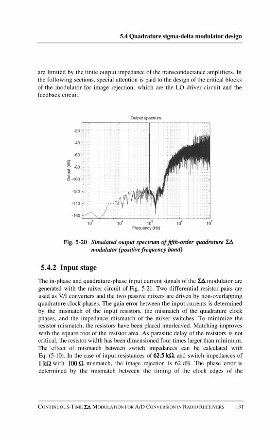
5.4 Quadrature sigma-delta modulator design
are limited by the finite output impedance of the transconductance amplifiers. Inthe following sections, special attention is paid to the design of the critical blocksof the modulator for image rejection, which are the LO driver circuit and thefeedback circuit.
5.4.2 Input stage
The in-phase and quadrature-phase input current signals of the modulator aregenerated with the mixer circuit of Fig. 5-21. Two differential resistor pairs areused as V/I converters and the two passive mixers are driven by non-overlappingquadrature clock phases. The gain error between the input currents is determinedby the mismatch of the input resistors, the mismatch of the quadrature clockphases, and the impedance mismatch of the mixer switches. To minimize theresistor mismatch, the resistors have been placed interleaved. Matching improveswith the square root of the resistor area. As parasitic delay of the resistors is notcritical, the resistor width has been dimensioned four times larger than minimum.The effect of mismatch between switch impedances can be calculated withEq. (5-10). In the case of input resistances of and switch impedances of
with mismatch, the image rejection is 62 dB. The phase error isdetermined by the mismatch between the timing of the clock edges of the
CONTINUOUS-TIME MODULATION FOR A/D CONVERSION IN RADIO RECEIVERS 131
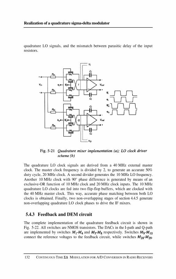
Realization of a quadrature sigma-delta modulator
quadrature LO signals, and the mismatch between parasitic delay of the inputresistors.
The quadrature LO clock signals are derived from a 40 MHz external masterclock. The master clock frequency is divided by 2, to generate an accurate 50%duty cycle, 20 MHz clock. A second divider generates the 10 MHz LO frequency.Another 10 MHz clock with 90° phase difference is generated by means of anexclusive-OR function of 10 MHz clock and 20 MHz clock inputs. The 10 MHzquadrature LO clocks are fed into two flip-flop buffers, which are clocked withthe 40 MHz master clock. This way, accurate phase matching between both LOclocks is obtained. Finally, two non-overlapping stages of section 4.4.5 generatenon-overlapping quadrature LO clock phases to drive the IF mixers.
5.4.3 Feedback and DEM circuit
The complete implementation of the quadrature feedback circuit is shown inFig. 5-22. All switches are NMOS transistors. The DACs in the I-path and Q-pathare implemented by switches and respectively. Switchesconnect the reference voltages to the feedback circuit, while switches
132 CONTINUOUS-TIME MODULATION FOR A/D CONVERSION IN RADIO RECEIVERS
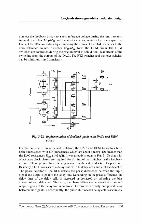
5.4 Quadrature sigma-delta modulator design
connect the feedback circuit to a zero reference voltage during the return-to-zerointerval. Switches are the reset switches, which clear the capacitiveloads of the D/A converters, by connecting the drains of the DAC switches to thezero reference source. Switches form the DEM circuit.The DEMswitches are controlled during the reset interval to shield non-ideal effects of theswitching from the outputs of the DACs. The RTZ switches and the reset switchescan be minimum-sized transistors.
For the purpose of linearity and isolation, the DAC and DEM transistors havebeen dimensioned with ON-impedances which are about a factor 100 smaller thanthe DAC resistances It was already shown in Fig. 5-17b that a lotof accurate clock phases are required for driving of the switches in the feedbackcircuit. These phases have been generated with a delay-locked loop circuit.Basically a DLL consists of a delay line with N delay cells and a phase detector.The phase detector of the DLL detects the phase difference between the inputsignal and output signal of the delay line. Depending on the phase difference, thedelay time of the delay cells is increased or decreased by adjusting the biascurrent of each delay cell. This way, the phase difference between the input andoutput signals of the delay line is controlled to zero, with exactly one period delaybetween the signals. Consequently, the phase shift of each delay cell is accurately
CONTINUOUS-TIME MODULATION FOR A/D CONVERSION IN RADIO RECEIVERS 133
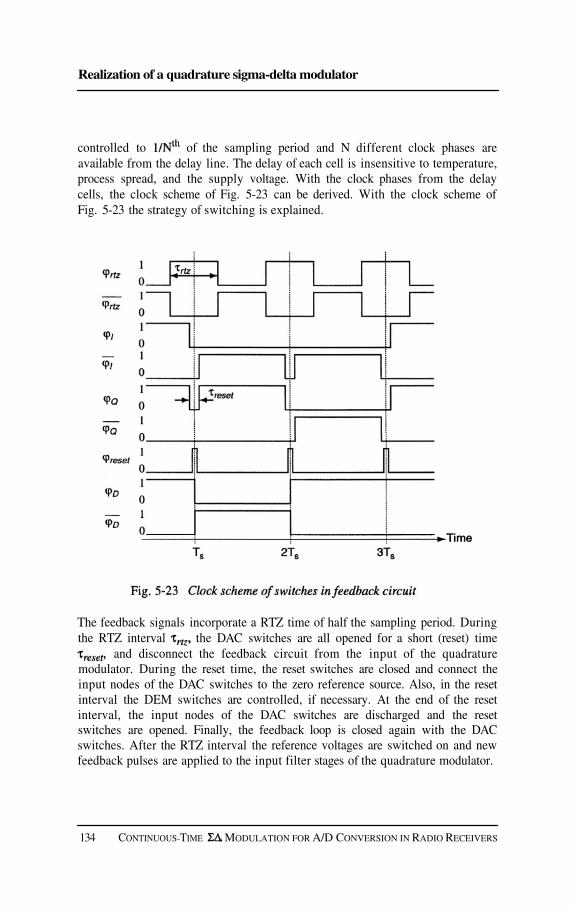
Realization of a quadrature sigma-delta modulator
controlled to of the sampling period and N different clock phases areavailable from the delay line. The delay of each cell is insensitive to temperature,process spread, and the supply voltage. With the clock phases from the delaycells, the clock scheme of Fig. 5-23 can be derived. With the clock scheme ofFig. 5-23 the strategy of switching is explained.
The feedback signals incorporate a RTZ time of half the sampling period. Duringthe RTZ interval the DAC switches are all opened for a short (reset) time
and disconnect the feedback circuit from the input of the quadraturemodulator. During the reset time, the reset switches are closed and connect theinput nodes of the DAC switches to the zero reference source. Also, in the resetinterval the DEM switches are controlled, if necessary. At the end of the resetinterval, the input nodes of the DAC switches are discharged and the resetswitches are opened. Finally, the feedback loop is closed again with the DACswitches. After the RTZ interval the reference voltages are switched on and newfeedback pulses are applied to the input filter stages of the quadrature modulator.
134 CONTINUOUS-TIME MODULATION FOR A/D CONVERSION IN RADIO RECEIVERS

5.5 Experimental results
5.5 Experimental results
In this section, the experimental results are given of a test chip (Fig. 5-24) forAM/FM radio which incorporates the complex modulator and the DEMcircuit as described in the previous section. The circuit has been designed in a
CMOS process using a single polysilicon layer and 5 metal layers. TheDEM circuit only occupies a small part of the total chip area. The samplingfrequency has been derived from a 42.1 MHz crystal oscillator and is 21.05 MHz.The LO frequency of the mixers is 10 MHz. All measurements have been done ata 3.3 V supply. The IF input signal at 10.1 MHz is generated by a Marconi multi-tone generator. The quadrature bitstream outputs (I and Q) are retrieved by an HP1673G logic analyzer. The output file with the I and Q data is processed withMATLAB (complex adding and FFT). The signal bandwidth of the complexmodulator is 300 kHz. In all measurement plots, the maximum input level hasbeen normalized to 0 dB. The resolution bandwidth of the measured spectra is40 Hz. Evaluation of the DEM algorithm involves two observations, which are theimage rejection ratio and the in-band noise level. For the testing of the DEMcircuit, the feedback resistors in the quadrature paths have been designed with a20% mismatch. With this large mismatch, any increase of noise within the signalband, as a result of the DEM algorithm, can be easily observed. Fig. 5-25 showsthe measured complex output spectrum of the quadrature modulator withoutthe DEM circuit operating. The signal tone is +100 kHz, while the imagecomponent is at -100 kHz. The measured image rejection is 20 dB which agreeswith a 20% mismatch. The small noise band around the +100 kHz signal carrier isphase noise from the external LO clock generator.
CONTINUOUS-TIME MODULATION FOR A/D CONVERSION IN RADIO RECEIVERS 135

Realization of a quadrature sigma-delta modulator
136 CONTINUOUS-TIME MODULATION FOR A/D CONVERSION IN RADIO RECEIVERS
5.5 Experimental results
In the next measurement, the DEM circuit is active and the feedback resistorswith the 20% mismatch are dynamically matched. Fig. 5-26 shows the measuredoutput spectrum. The same input signal is applied as in the previousmeasurement. Clearly, the image component has dropped down considerably. Themeasured image rejection ratio is 60 dB, which is an improvement of 40 dB.Moreover, compared to Fig. 5-25, no increased noise level can be observed in thesignal band when the DEM circuit is active. The image rejection ratio is limitedby the mismatch in other parts of the circuit such as the input resistors, mixers,LO signals, and the DEM and DAC switches.
Next, measurements have been done with two FM input signals at 10.1 Mhz(image channel) and 9.9 MHz (desired channel) with 100 kHz and 25 kHzbandwidths respectively. The maximum levels of the downconverted image (at+ 100 kHz) and desired (at -100 kHz) channels are -25 dB and -60 dBrespectively. Fig. 5-27 shows the measured spectrum without DEM (20% initialmismatch). The desired channel at -100 kHz is not visible as it is concealedcompletely by the large -45 dB image leakage signal. Fig. 5-28 shows the samemeasurement, now with the DEM circuit operating. The leaked image componenthas dropped more than 40 dB and the desired channel at -100 kHz can be detectedclearly. This measurement shows that the DEM circuit is also working for multi-tone FM input signals.
The IRRs of a batch of 37 test chips have been measured and the distribution ofthe measured results are shown in Fig. 5-29. All measured chips show an IRRbetter than 55 dB with DEM. From the figure it can be observed that the typicalIRR is in the order of 60 dB with the DEM circuit. The straight line in Fig. 5-29 isan ideal normal distribution. The measured values closely match the ideal normaldistribution with a likelihood of 98.8%. In case of a normal distribution, a mean
and sigma value can be calculated which are 63 dB and 4.5 dB for thesemeasured values.
CONTINUOUS-TIME MODULATION FOR A/D CONVERSION IN RADIO RECEIVERS 137

Realization of a quadrature sigma-delta modulator
138 CONTINUOUS-TIME MODULATION FOR A/D CONVERSION IN RADIO RECEIVERS

5.6 Conclusions
5.6 Conclusions
In this chapter, a DEM algorithm is presented that uses the quadrature bitstreamoutputs of a complex modulator. According to this DEM algorithm, thequadrature feedback paths of the modulator can be dynamically matchedwithout causing demodulation of high frequency quantization noise, as is the casewith traditional DEM techniques (fixed frequency or pseudo-random). The DEMsignal is generated using an EXOR port that calculates the product of the I and Qbitstream signals. With this DEM algorithm, the error spectrum due to amismatch between the quadrature feedback paths, is mirrored relative to DC.
A CMOS prototype test chip with DEM circuit has been designed. Alarge systematic mismatch of 20% has been applied between the I and Q feedbackresistors. Without DEM, the measured IR ratio is 20 dB, which agrees with the20% mismatch. With DEM, the measured IR ratio is better than 55 dB for 37different samples. No increased in-band noise level is observed, even with thelarge initial 20% mismatch. The prototype test chip was designed to test the DEMalgorithm in the feedback path only, and no compensation techniques have been
CONTINUOUS-TIME MODULATION FOR A/D CONVERSION IN RADIO RECEIVERS 139

Realization of a quadrature sigma-delta modulator
applied to improve the matching between the input circuits of the quadraturemodulator (input resistors, mixers and LO drivers). Therefore, the image rejectionis limited by the matching between these circuits to a typical value of 63 dB for37 measured samples.
140 CONTINUOUS-TIME MODULATION FOR A/D CONVERSION IN RADIO RECEIVERS
5.6 Conclusions
Zwan, E.J. van der, K. Philips, C. Bastiaanse, “A 10.7 MHz IF-to-Baseband A/D Conversion System for AM/FM RadioReceivers,” ISSCC Dig. Tech. Papers, pp. 340-341, Feb. 2000.Carley, L.R., “A noise-shaping coder topology for 15+ bitconverters,” IEEE J. Solid-State Circuits, vol. 24, pp. 267-273, Apr.1989.Breems, L.J., E.C. Dijkmans, J.H. Huijsing, “A Quadrature Data-Dependent DEM Algorithm to Improve Image Rejection of aComplex Modulator,” ISSCC Dig. Tech. Papers, pp. 48-49, Feb.2001.
References
[5.1]
[5.2]
[5.3]
CONTINUOUS-TIME MODULATION FOR A/D CONVERSION IN RADIO RECEIVERS 141

Benchmark
6
6.1 Introduction
In this book, some designs of low-power, high-performance IF-to-baseband A/Dconverters based on the principle of modulation are described. Optimizing theperformance-to-power ratio, which is expressed by the FOMs in chapter 2, isdone at three levels in the design process. In chapter 2, some system architecturesare discussed which put different requirements on the A/D converter. Theapproach of this book is that IF-to-baseband A/D conversion can be performedwith low-power and high-performance by combining a mixer with a continuous-time lowpass modulator. At the circuit level, an integrated filter and passivemixer design is proposed in chapter 4 that provides highly linear mixing at thecost of no extra power. Finally, at the transistor level, relations between distortionand design parameters have been derived to optimize the performance-to-powerratio. As mixing is done in the analog domain, good matching is required betweenthe quadrature paths of the IF-to-baseband A/D converter for a sufficient amountof image rejection. Therefore, in chapter 5, a dynamic element matchingalgorithm is presented that improves matching between the quadrature feedbackpaths of the IF-to-baseband modulator. In chapters 4 and 5, the designs andexperimental results of some test chips are presented. Special attention has beenpaid to the linearity of the modulators and matching performance of thequadrature paths.
CONTINUOUS-TIME MODULATION FOR A/D CONVERSION IN RADIO RECEIVERS 143

Benchmark
6.2 Benchmark of test chips
To put the results of the test chips in the book in perspective, the measuredperformance is compared with that of other designs found in literature. First, theperformance of the lowpass modulator of section 4.5.1 is investigated. Forcomparison of the different sigma-delta modulators the figure-of-merit ofEq. (2-6) has been used. The results of the benchmark are listed in Table 6-1. Thetop reference is the test chip of section 4.5.1 and the other references are allsigma-delta modulators from literature. Other types of A/D converters are notincluded in the list. For some papers, the SNDR has been determined from themeasurement plots, in case the number was not published. Moreover, only thepower consumption of the sigma-delta modulator has been taken into account(power of digital decimation filters not included). The different modulator typesare continuous-time (CT), switched-capacitor (SC), and switched-opamp (SO).
144 CONTINUOUS-TIME MODULATION FOR A/D CONVERSION IN RADIO RECEIVERS
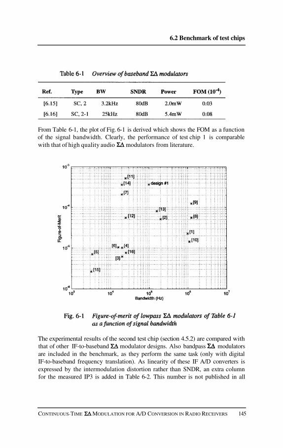
6.2 Benchmark of test chips
From Table 6-1, the plot of Fig. 6-1 is derived which shows the FOM as a functionof the signal bandwidth. Clearly, the performance of test chip 1 is comparablewith that of high quality audio modulators from literature.
The experimental results of the second test chip (section 4.5.2) are compared withthat of other IF-to-baseband modulator designs. Also bandpass modulatorsare included in the benchmark, as they perform the same task (only with digitalIF-to-baseband frequency translation). As linearity of these IF A/D converters isexpressed by the intermodulation distortion rather than SNDR, an extra columnfor the measured IP3 is added in Table 6-2. This number is not published in all
CONTINUOUS-TIME MODULATION FOR A/D CONVERSION IN RADIO RECEIVERS 145

Benchmark
references, and for some designs, the IP3 is calculated from the measuredintermodulation distortion. The different types are lowpass modulators withmixer (LPM), bandpass modulators (BP), and bandpass modulators with mixer(BPM). The fourth column of Table 6-2 shows the input IF. To be able to compareall designs, the FOM is based on the DR (Eq. (2-5)).
Fig. 6-2 shows the FOMs of the IF-to-baseband modulators of Table 6-2 as afunction of the intermediate frequency of the input signal. The FOM of test chip 2is more than a factor of 20 larger than the best reported bandpass modulator inTable 6-2. Also linearity performance, which is not included in the FOM, is muchhigher than that of the other designs. The main advantage of a bandpassmodulator is the excellent image rejection performance. This does not apply topseudo n-path designs [6.21] which have a finite image rejection ratio.
146 CONTINUOUS-TIME MODULATION FOR A/D CONVERSION IN RADIO RECEIVERS
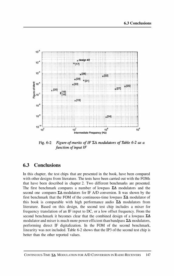
6.3 Conclusions
6.3 Conclusions
In this chapter, the test chips that are presented in the book, have been comparedwith other designs from literature. The tests have been carried out with the FOMsthat have been described in chapter 2. Two different benchmarks are presented.The first benchmark compares a number of lowpass modulators and thesecond one compares modulators for IF A/D conversion. It was shown by thefirst benchmark that the FOM of the continuous-time lowpass modulator ofthis book is comparable with high performance audio modulators fromliterature. Based on this design, the second test chip includes a mixer forfrequency translation of an IF input to DC, or a low offset frequency. From thesecond benchmark it becomes clear that the combined design of a lowpassmodulator and mixer is much more power efficient than bandpass modulators,performing direct IF digitalization. In the FOM of the second benchmark,linearity was not included. Table 6-2 shows that the IP3 of the second test chip isbetter than the other reported values.
CONTINUOUS-TIME MODULATION FOR A/D CONVERSION IN RADIO RECEIVERS 147

Benchmark
The results of the benchmark are in agreement with the conclusions of chapter 2,where it was elaborated that it is more difficult to achieve good linearity, dynamicrange and power efficiency at high frequencies than at low frequencies. With theuse of dynamic element matching, high accuracy can be achieved in analogcircuits as well. With the techniques that have been presented in this book, a highperformance and power efficient IF A/D converter is obtained. Such an A/Dconverter is a key element that is required for highly integrated receivers.
148 CONTINUOUS-TIME MODULATION FOR A/D CONVERSION IN RADIO RECEIVERS

6.3 Conclusions
References
[6.1]
[6.2]
[6.3]
[6.4]
[6.5]
[6.6]
[6.7]
[6.8]
[6.9]
[6.10]
[6.11]
Marques, A.M., V. Peluso, M.S.J. Steyaert, W. Sansen, “A 15-bResolution 2-MHz Nyquist Rate ADC in a CMOSTechnology,” IEEE J. Solid-State Circuits, vol. 33, pp. 1065-1075,Jul. 1998.Thanh, C.K., S.H. Lewis, P.J. Hurst, “A Second-Order Double-Sampled Delta-Sigma Modulator Using Individual-LevelAveraging,” IEEE J. Solid-State Circuits, vol. 32, pp. 1269-1273,Aug. 1997.Chen, F. B.H. Leung, “A High Resolution Multibit Sigma-DeltaModulator with Individual Level Averaging,” IEEE J. Solid-StateCircuits, vol. 30, pp. 453-460, Apr. 1995.Burmas, T.V., K.C. Dyer, P.J. Hurst, S.H. Lewis, “A Second-OrderDouble-Sampled Delta-Sigma Modulator Using Additive-ErrorSwitching,” IEEE J. Solid-State Circuits, vol. 31, pp. 284-293, Mar.1996.Zwan, E.J. van der, E.C. Dijkmans, “A 0.2-mW CMOSModulator for Speech Coding with 80 dB Dynamic Range,” IEEE J.Solid-State Circuits, vol. 31, pp. 1873-1880, Dec. 1996.Peluso, V., P. Vancorenland, A. Marques, M. Steyaert, W. Sansen,“A 900 mV Switched Opamp Modulator with 77 dBDynamic Range,” ISSCC Dig. Tech. Papers, pp. 68-69, Feb. 1998.Coban, A.L., P.E. Allen, “A 1.5V 1.0 mW Audio Modulatorwith 98 dB Dynamic Range” ISSCC Dig. Tech. Papers, pp. 50-51,Feb. 1999.Geerts, Y., M. Steyaert, W. Sansen, “A 2.5 Msample/s Multi-bitCMOS ADC with 95 dB SNR,” ISSCC Dig. Tech. Papers, pp. 336-337, Feb. 2000.Fujimori, I. L. Longo, A. Hairapetian, K. Seiyama, S. Kosic, J. Cao,S. Chan, “A 90 dB SNR, 2.5 MHz Output Rate ADC using cascadedMultibit Modulation at 8x Oversampling Ratio,” ISSCC Dig.Tech. Papers, pp. 338-339, Feb. 2000.Geerts, Y., A. Marques, M. Steyaert, W. Sansen, “A 3.3 V 15-bitDelta-Sigma ADC with a Signal Bandwidth of 1.1 MHz for ADSL-Applications,” Proc. of ESSCIRC, pp. 168-171, Sep. 1998.Rabii, S., B.A. Wooley, “A 1.8-V Digital-Audio Sigma-DeltaModulator in CMOS,” IEEE J. Solid-State Circuits, vol. 32,pp. 783-796, Jun. 1997.
CONTINUOUS-TIME MODULATION FOR A/D CONVERSION IN RADIO RECEIVERS 149

Benchmark
[6.12]
[6.13]
[6.14]
[6.15]
[6.16]
[6.17]
[6.18]
[6.19]
[6.20]
[6.21]
[6.22]
[6.23]
[6.24]
[6.25]
Williams, L.A., B.A. Wooley, “A Third-Order Sigma-DeltaModulator with Extended Dynamic Range,” IEEE J. Solid-StateCircuits, vol. 29, pp. 193-202, Mar. 1994.Yin, G., F. Stubbe, W. Sansen, “A 16-b 320-kHz CMOS A/DConverter Using Two-Stage Third-Order Noise Shaping,” IEEEJ. Solid-State Circuits, vol. 28, pp. 640-647, Jun. 1993.Zwan, E.J. van der, “A 2.3 mW CMOS Modulator for AudioApplications,” ISSCC Dig. Tech. Papers, pp. 220-221, Feb. 1997.Grilo, J., E. MacRobbie, R. Halim, G. Temes, “A 1.8V 94 dBDynamic Range Modulator for Voice Applications,” ISSCC Dig.Tech. Papers, pp. 230-231, Feb. 1996.Rabii, S., B.A. Wooley, “A 1.8V, 5.4 mW, Digital-AudioModulator in CMOS,” ISSCC Dig. Tech. Papers, pp. 228-229, Feb. 1996.CHen, F., and B. Leung, “A 0.25 mW Low-Pass Passive Sigma-Delta Modulator with Built-in Mixer for a 10-MHz IF Input,” IEEEJ. Solid-State Circuits, vol. 32, pp. 774-782, Jun. 1997.Jantzi, S.A., K.W. Martin, and A.S. Sedra, “Quadrature Bandpass
Modulation for Digital Radio,” IEEE J. Solid-State Circuits, vol.32, pp. 1935-1950, Dec. 1997.Singor, F.W. and W.M. Snelgrove, “Switched-Capacitor BandpassDelta-Sigma A/D Modulation at 10.7 MHz,” IEEE J. Solid-StateCircuits, vol. 30, pp. 184-192, March 1995.Song, B.S., “A Fourth-Order Bandpass Delta-Sigma Modulator withReduced Number of Op Amps,” IEEE J. Solid-State Circuits, vol.30, pp. 1309-1315, Dec. 1995.Ong, A.K. and B.A. Wooley, “A Two-Path Bandpass Modulatorfor Digital IF Extraction at 20 MHz,” IEEE J. Solid-State Circuits,vol. 32, pp. 1920-1934, Dec. 1997.Hairapetian, A., “An 81 MHz IF Receiver in CMOS,“ ISSCC Dig.Tech. Papers, pp. 56-57, Feb. 1996.Engelen, J. van, R. van de Plassche, E. Stikvoort, A. Venes, “A 6th-Order Continuous-Time Bandpass Modulator for Digital RadioIF,“ ISSCC Dig. Tech. Papers, pp. 56-57, Feb. 1999.Tao, H., J.M. Khoury, “A 100 MHz IF, 400 M Sample/S CMOSDirect-Conversion Bandpass Modulator,” ISSCC Dig. Tech.Papers, pp. 60-61, Feb. 1999.Namdar, A., B.H. Leung, “A 400 MHz 12 b 18 mW IF Digitizerwith Mixer Inside a Modulator Loop,” ISSCC Dig. Tech. Papers,pp. 62-63, Feb. 1999.
150 CONTINUOUS-TIME MODULATION FOR A/D CONVERSION IN RADIO RECEIVERS
6.3 Conclusions
[6.26]
[6.27]
[6.28]
Tabatabaei, A., K. Kaviani, B. Wooley, “A Two-Path BandpassModulator with Extended Noise Shaping,” ISSCC Dig. Tech.Papers, pp. 342-343, Feb. 2000.Maurino, R., P. Mole, “A 200 MHz IF, 11 bit, order Band-Pass
ADC in SiGe,” Proc. of ESSCIRC, pp. 74-77, Sep. 1999.Tonietto, D., P. Cusinato, F. Stefani, A. Baschirotto, “A 3.3VCMOS 10.7 MHz 6th-order bandpass modulator with 78 dBdynamic range,” Proc. of ESSCIRC, pp. 78-81, Sep. 1999.
CONTINUOUS-TIME MODULATION FOR A/D CONVERSION IN RADIO RECEIVERS 151

Index
AA/D converter 97accumulator 3aliasing 44AM/FM radio 22, 129analog signals 3anti-aliasing filter 11autocorrelation 35
Bbandpass A/D conversion 13base station 13benchmark 144Butterworth filter 56
Cceramic filter 11channel filter 11characteristic equation 48, 54charge injection 125chip micrograph 99, 135clock feedthrough 88comparator 90complex data-controlled DEM 117complex filter 66complex integrator 64cross-modulation distortion 17
DD/A converter 97, 133decimation filter 4degeneration 96delay-locked loop 133delta modulator 29
DEM circuit 133DEM control signal 114digital receiver 14digital signal processor 9distortion 80, 93, 100dither 35dynamic element matching 15, 111dynamic range 16, 102
Ffeedback compensation 60feedforward compensation 54figure-of-merit 21, 144
GGSM band 22
Hharmonic distortion 17, 37high frequency stability 53higher-order filters 53
IIF digitizing 13
CONTINUOUS-TIME MODULATION FOR A/D CONVERSION IN RADIO RECEIVERS 153
IF-to-baseband modulator 73image interference 19, 67, 113image rejection 20, 110, 135integrator 3, 30, 90interference signals 9intermediate frequency 11intermodulation distortion 17, 105, 145intermodulation intercept point 17intersymbol interference 41inverse Chebyshev 59
Index
Jjitter 43, 105
Llarge signal stability 51latch 97limit cycle 49limiter 52linear region 81local oscillator 11, 82low-IF 12, 129
Mmatching 111measurement setup 100mismatch 123mixer 11, 80, 131mixer inside the sigma-delta loop 74mixer outside the sigma-delta loop 77
Nnoise transfer function 32noise-shaping 3, 30non-linear transconductance 93non-linearity 17non-overlapping clock 83, 98, 103numerical model 5Nyquist frequency 3
Ooffset 33, 87opamp 92OTA 96overlapping clock 83overload 52, 102oversampling 3, 30oversampling ratio 31
Pparasitic delay 111passive mixer 79, 80peak SNR 16peaking 63phase noise 43phase uncertainty 47
power consumption 22, 144pseudorandom 115
Qquadrature LO clock 110, 132quadrature mixing 11quadrature modulator 110quadrature signals 110quantization error 3, 31quantization noise 31quantizer 47
RRC integrator 90resolution 3, 16resonator 59, 129return-to-zero 42, 76root locus 48
Ssampling rate 3SAW filter 11selectivity 9self-mixing 88, 126sensitivity 9signal bandwidth 3signal transfer function 32signal-to-noise ratio 16signal-to-noise-and-distortion ratio 17small signal stability 46spurious-free dynamic range 17stability 46superheterodyne receiver 11switch impedance 80
Tthermal noise 95third harmonic distortion 39, 95tones 33, 102transconductance-C integrator 96
Wwaveform asymmetry 41white noise 30
154 CONTINUOUS-TIME MODULATION FOR A/D CONVERSION IN RADIO RECEIVERS

Index
Zzero-IF 12zero-order hold 48
CONTINUOUS-TIME MODULATION FOR A/D CONVERSION IN RADIO RECEIVERS 155